EP1995770A1 - Method of seasoning film-forming apparatus - Google Patents
Method of seasoning film-forming apparatus Download PDFInfo
- Publication number
- EP1995770A1 EP1995770A1 EP07714447A EP07714447A EP1995770A1 EP 1995770 A1 EP1995770 A1 EP 1995770A1 EP 07714447 A EP07714447 A EP 07714447A EP 07714447 A EP07714447 A EP 07714447A EP 1995770 A1 EP1995770 A1 EP 1995770A1
- Authority
- EP
- European Patent Office
- Prior art keywords
- film
- processing chamber
- silicon nitride
- silicon
- forming apparatus
- Prior art date
- Legal status (The legal status is an assumption and is not a legal conclusion. Google has not performed a legal analysis and makes no representation as to the accuracy of the status listed.)
- Withdrawn
Links
- 238000000034 method Methods 0.000 title claims abstract description 47
- 235000011194 food seasoning agent Nutrition 0.000 title claims abstract description 25
- 239000007789 gas Substances 0.000 claims abstract description 34
- 239000000758 substrate Substances 0.000 claims abstract description 30
- 229910052581 Si3N4 Inorganic materials 0.000 claims abstract description 26
- HQVNEWCFYHHQES-UHFFFAOYSA-N silicon nitride Chemical compound N12[Si]34N5[Si]62N3[Si]51N64 HQVNEWCFYHHQES-UHFFFAOYSA-N 0.000 claims abstract description 26
- 238000004140 cleaning Methods 0.000 claims abstract description 16
- 238000000151 deposition Methods 0.000 claims abstract description 16
- IJGRMHOSHXDMSA-UHFFFAOYSA-N Atomic nitrogen Chemical compound N#N IJGRMHOSHXDMSA-UHFFFAOYSA-N 0.000 claims abstract description 14
- 230000015572 biosynthetic process Effects 0.000 claims abstract description 11
- 229910021417 amorphous silicon Inorganic materials 0.000 claims abstract description 9
- 229910052757 nitrogen Inorganic materials 0.000 claims abstract description 7
- XUIMIQQOPSSXEZ-UHFFFAOYSA-N Silicon Chemical compound [Si] XUIMIQQOPSSXEZ-UHFFFAOYSA-N 0.000 claims description 8
- 229910052710 silicon Inorganic materials 0.000 claims description 8
- 239000010703 silicon Substances 0.000 claims description 8
- QJGQUHMNIGDVPM-UHFFFAOYSA-N nitrogen group Chemical group [N] QJGQUHMNIGDVPM-UHFFFAOYSA-N 0.000 claims description 6
- 238000005530 etching Methods 0.000 claims description 5
- 239000002245 particle Substances 0.000 abstract description 24
- 229910020776 SixNy Inorganic materials 0.000 description 15
- 230000007704 transition Effects 0.000 description 6
- 239000004065 semiconductor Substances 0.000 description 4
- QGZKDVFQNNGYKY-UHFFFAOYSA-N Ammonia Chemical compound N QGZKDVFQNNGYKY-UHFFFAOYSA-N 0.000 description 3
- BLRPTPMANUNPDV-UHFFFAOYSA-N Silane Chemical compound [SiH4] BLRPTPMANUNPDV-UHFFFAOYSA-N 0.000 description 3
- XKRFYHLGVUSROY-UHFFFAOYSA-N Argon Chemical compound [Ar] XKRFYHLGVUSROY-UHFFFAOYSA-N 0.000 description 2
- 238000005229 chemical vapour deposition Methods 0.000 description 2
- 239000011248 coating agent Substances 0.000 description 2
- 238000000576 coating method Methods 0.000 description 2
- 230000008021 deposition Effects 0.000 description 2
- 238000010586 diagram Methods 0.000 description 2
- 238000005259 measurement Methods 0.000 description 2
- GVGCUCJTUSOZKP-UHFFFAOYSA-N nitrogen trifluoride Chemical compound FN(F)F GVGCUCJTUSOZKP-UHFFFAOYSA-N 0.000 description 2
- 238000005268 plasma chemical vapour deposition Methods 0.000 description 2
- 238000005086 pumping Methods 0.000 description 2
- XAGFODPZIPBFFR-UHFFFAOYSA-N aluminium Chemical compound [Al] XAGFODPZIPBFFR-UHFFFAOYSA-N 0.000 description 1
- 229910052782 aluminium Inorganic materials 0.000 description 1
- 229910021529 ammonia Inorganic materials 0.000 description 1
- 229910052786 argon Inorganic materials 0.000 description 1
- 239000000919 ceramic Substances 0.000 description 1
- 239000000356 contaminant Substances 0.000 description 1
- 230000000694 effects Effects 0.000 description 1
- ZZUFCTLCJUWOSV-UHFFFAOYSA-N furosemide Chemical compound C1=C(Cl)C(S(=O)(=O)N)=CC(C(O)=O)=C1NCC1=CC=CO1 ZZUFCTLCJUWOSV-UHFFFAOYSA-N 0.000 description 1
- 230000000977 initiatory effect Effects 0.000 description 1
- 238000010030 laminating Methods 0.000 description 1
- QKCGXXHCELUCKW-UHFFFAOYSA-N n-[4-[4-(dinaphthalen-2-ylamino)phenyl]phenyl]-n-naphthalen-2-ylnaphthalen-2-amine Chemical compound C1=CC=CC2=CC(N(C=3C=CC(=CC=3)C=3C=CC(=CC=3)N(C=3C=C4C=CC=CC4=CC=3)C=3C=C4C=CC=CC4=CC=3)C3=CC4=CC=CC=C4C=C3)=CC=C21 QKCGXXHCELUCKW-UHFFFAOYSA-N 0.000 description 1
- 238000005121 nitriding Methods 0.000 description 1
- 229910000069 nitrogen hydride Inorganic materials 0.000 description 1
- 239000002994 raw material Substances 0.000 description 1
- 229910000077 silane Inorganic materials 0.000 description 1
- 230000006641 stabilisation Effects 0.000 description 1
- 238000011105 stabilization Methods 0.000 description 1
- 230000000087 stabilizing effect Effects 0.000 description 1
Images

Classifications
-
- C—CHEMISTRY; METALLURGY
- C23—COATING METALLIC MATERIAL; COATING MATERIAL WITH METALLIC MATERIAL; CHEMICAL SURFACE TREATMENT; DIFFUSION TREATMENT OF METALLIC MATERIAL; COATING BY VACUUM EVAPORATION, BY SPUTTERING, BY ION IMPLANTATION OR BY CHEMICAL VAPOUR DEPOSITION, IN GENERAL; INHIBITING CORROSION OF METALLIC MATERIAL OR INCRUSTATION IN GENERAL
- C23C—COATING METALLIC MATERIAL; COATING MATERIAL WITH METALLIC MATERIAL; SURFACE TREATMENT OF METALLIC MATERIAL BY DIFFUSION INTO THE SURFACE, BY CHEMICAL CONVERSION OR SUBSTITUTION; COATING BY VACUUM EVAPORATION, BY SPUTTERING, BY ION IMPLANTATION OR BY CHEMICAL VAPOUR DEPOSITION, IN GENERAL
- C23C16/00—Chemical coating by decomposition of gaseous compounds, without leaving reaction products of surface material in the coating, i.e. chemical vapour deposition [CVD] processes
- C23C16/44—Chemical coating by decomposition of gaseous compounds, without leaving reaction products of surface material in the coating, i.e. chemical vapour deposition [CVD] processes characterised by the method of coating
- C23C16/4401—Means for minimising impurities, e.g. dust, moisture or residual gas, in the reaction chamber
- C23C16/4404—Coatings or surface treatment on the inside of the reaction chamber or on parts thereof
-
- C—CHEMISTRY; METALLURGY
- C23—COATING METALLIC MATERIAL; COATING MATERIAL WITH METALLIC MATERIAL; CHEMICAL SURFACE TREATMENT; DIFFUSION TREATMENT OF METALLIC MATERIAL; COATING BY VACUUM EVAPORATION, BY SPUTTERING, BY ION IMPLANTATION OR BY CHEMICAL VAPOUR DEPOSITION, IN GENERAL; INHIBITING CORROSION OF METALLIC MATERIAL OR INCRUSTATION IN GENERAL
- C23C—COATING METALLIC MATERIAL; COATING MATERIAL WITH METALLIC MATERIAL; SURFACE TREATMENT OF METALLIC MATERIAL BY DIFFUSION INTO THE SURFACE, BY CHEMICAL CONVERSION OR SUBSTITUTION; COATING BY VACUUM EVAPORATION, BY SPUTTERING, BY ION IMPLANTATION OR BY CHEMICAL VAPOUR DEPOSITION, IN GENERAL
- C23C16/00—Chemical coating by decomposition of gaseous compounds, without leaving reaction products of surface material in the coating, i.e. chemical vapour deposition [CVD] processes
- C23C16/02—Pretreatment of the material to be coated
- C23C16/0227—Pretreatment of the material to be coated by cleaning or etching
- C23C16/0236—Pretreatment of the material to be coated by cleaning or etching by etching with a reactive gas
-
- C—CHEMISTRY; METALLURGY
- C23—COATING METALLIC MATERIAL; COATING MATERIAL WITH METALLIC MATERIAL; CHEMICAL SURFACE TREATMENT; DIFFUSION TREATMENT OF METALLIC MATERIAL; COATING BY VACUUM EVAPORATION, BY SPUTTERING, BY ION IMPLANTATION OR BY CHEMICAL VAPOUR DEPOSITION, IN GENERAL; INHIBITING CORROSION OF METALLIC MATERIAL OR INCRUSTATION IN GENERAL
- C23C—COATING METALLIC MATERIAL; COATING MATERIAL WITH METALLIC MATERIAL; SURFACE TREATMENT OF METALLIC MATERIAL BY DIFFUSION INTO THE SURFACE, BY CHEMICAL CONVERSION OR SUBSTITUTION; COATING BY VACUUM EVAPORATION, BY SPUTTERING, BY ION IMPLANTATION OR BY CHEMICAL VAPOUR DEPOSITION, IN GENERAL
- C23C16/00—Chemical coating by decomposition of gaseous compounds, without leaving reaction products of surface material in the coating, i.e. chemical vapour deposition [CVD] processes
- C23C16/02—Pretreatment of the material to be coated
- C23C16/0272—Deposition of sub-layers, e.g. to promote the adhesion of the main coating
- C23C16/029—Graded interfaces
-
- C—CHEMISTRY; METALLURGY
- C23—COATING METALLIC MATERIAL; COATING MATERIAL WITH METALLIC MATERIAL; CHEMICAL SURFACE TREATMENT; DIFFUSION TREATMENT OF METALLIC MATERIAL; COATING BY VACUUM EVAPORATION, BY SPUTTERING, BY ION IMPLANTATION OR BY CHEMICAL VAPOUR DEPOSITION, IN GENERAL; INHIBITING CORROSION OF METALLIC MATERIAL OR INCRUSTATION IN GENERAL
- C23C—COATING METALLIC MATERIAL; COATING MATERIAL WITH METALLIC MATERIAL; SURFACE TREATMENT OF METALLIC MATERIAL BY DIFFUSION INTO THE SURFACE, BY CHEMICAL CONVERSION OR SUBSTITUTION; COATING BY VACUUM EVAPORATION, BY SPUTTERING, BY ION IMPLANTATION OR BY CHEMICAL VAPOUR DEPOSITION, IN GENERAL
- C23C16/00—Chemical coating by decomposition of gaseous compounds, without leaving reaction products of surface material in the coating, i.e. chemical vapour deposition [CVD] processes
- C23C16/44—Chemical coating by decomposition of gaseous compounds, without leaving reaction products of surface material in the coating, i.e. chemical vapour deposition [CVD] processes characterised by the method of coating
- C23C16/4401—Means for minimising impurities, e.g. dust, moisture or residual gas, in the reaction chamber
- C23C16/4405—Cleaning of reactor or parts inside the reactor by using reactive gases
-
- H—ELECTRICITY
- H01—ELECTRIC ELEMENTS
- H01J—ELECTRIC DISCHARGE TUBES OR DISCHARGE LAMPS
- H01J37/00—Discharge tubes with provision for introducing objects or material to be exposed to the discharge, e.g. for the purpose of examination or processing thereof
- H01J37/32—Gas-filled discharge tubes
- H01J37/32431—Constructional details of the reactor
- H01J37/32798—Further details of plasma apparatus not provided for in groups H01J37/3244 - H01J37/32788; special provisions for cleaning or maintenance of the apparatus
- H01J37/32853—Hygiene
- H01J37/32862—In situ cleaning of vessels and/or internal parts
Definitions
- the present invention relates to a seasoning method for a film-forming apparatus, which is suitable for a plasma CVD apparatus or the like configured to form films constituting a semiconductor device, for example.
- films are formed on a substrate by use of a film-forming apparatus such as a plasma CVD apparatus.
- films to be formed are attached not only onto the substrate but also onto an inner wall of a processing chamber of the film-forming apparatus.
- the films attached to the inner wall of the processing chamber are further deposited thereon each time films are formed on the substrate, and are peeled off if they are left intact and may cause particles. Accordingly, plasma cleaning is periodically performed to remove the unnecessary films attached to the inner wall.
- a film formation process for a predetermined amount is usually performed with no substrate while formed under the same conditions as film formation on the substrate (seasoning).
- the film itself has high stress and low adhesion to the inner wall of the processing chamber. Therefore, the film is apt to be peeled off from the inner wall of the processing chamber, and to become particles, thereby leading to a problem that the generation of particles cannot be reduced.
- the present invention has been made in view of the foregoing problem and aims at providing a seasoning method for a film-forming apparatus configured to reduce the generation of particles.
- a seasoning method for a film-forming apparatus described in a first invention to solve the above problem is a seasoning method for a film-forming apparatus configured to form a silicon nitride film on a substrate placed in a processing chamber, comprising: supplying a cleaning gas into the processing chamber, and etching the silicon nitride film attached to an inner wall of the processing chamber while converting the cleaning gas into a plasma state; supplying a silicon-containing gas into the processing chamber, and depositing an amorphous silicon film on the inner wall of the processing chamber while converting the silicon-containing gas into a plasma state; supplying the silicon-containing gas into the processing chamber, while supplying a nitrogen-containing gas in a gradually increasing manner up to a predetermined flow rate, and thus depositing, on the amorphous silicon film, a silicon nitride film with the nitrogen content gradually increasing in a thickness direction, while converting the silicon-containing gas and the nitrogen-containing gas into a plasma state; and supplying a rare gas into the processing chamber, and
- a seasoning method for a film-forming apparatus described in a second invention to solve the above problem is the seasoning method for a film-forming apparatus according to the first invention, wherein the nitrogen-containing gas is supplied in a gradually increasing manner up to the predetermined flow rate gently in the beginning and more rapidly thereafter when depositing the silicon nitride film on the amorphous silicon film.
- the amorphous silicon film is deposited after performing plasma cleaning (etching) of the film attached to the inner wall of the processing chamber, and the silicon nitride film in which the nitrogen content is gradually increased in the thickness direction is deposited thereon. Moreover, the inside of the processing chamber is maintained with the rare gas plasma until film formation on the substrate is initiated. Therefore, it is possible to reduce particles at the time of film formation on the substrate.
- a seasoning method for a film-forming apparatus according to the present invention will be described in detail by using Fig. 1 to Fig. 4(c) .
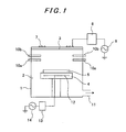
- Fig. 1 is a schematic configuration diagram showing an example of an embodiment of a film-forming apparatus according to the present invention.
- a cylindrical vacuum chamber 1 made of aluminum is configured to serve as a processing chamber 2 (a treatment vessel), and a discoid ceiling plate 3 made of a ceramic constituting an electromagnetic wave transmissive window is disposed on an upper opening portion of the vacuum chamber 1 so as to occlude the opening portion.
- a support table 4 is provided in the lower part of the vacuum chamber 1 and a substrate 5 such as a semiconductor is placed on an upper surface of the support table 4.
- High-frequency antennas 7 made of circular rings, for example, are disposed on an upper part of the ceiling plate 3, and a high-frequency power source 9 for plasma generation is connected to one of the high-frequency antennas 7 through a matching box 8 configured to perform impedance matching.
- the vacuum chamber 1 is provided with gas nozzles 10a and 10b for introducing desired gases into the processing chamber 2, and is also provided with an exhaust port 11.
- the exhaust port 11 is connected to an unillustrated vacuum pumping system, and the inside of the processing chamber 2 is controlled to a desired pressure by using this vacuum pumping system.
- the support table 4 for supporting the substrate 5 is provided with an antenna 12.
- An alternating-current power source 14 for biasing is connected to this antenna 12 through a matching box 13 configured to perform impedance matching.
- the antenna 12 functions as a bias electrode for applying bias power to the substrate 5.
- the film-forming apparatus having the above-described configuration, by supplying high-frequency power from the high-frequency power source 9 to the high-frequency antenna 7, an electromagnetic wave from the high-frequency antenna 7 passes through the ceiling plate 3, and is made incident on the processing chamber 2.
- the gases introduced into the processing chamber 2 through the gas nozzles 10a and 10b are ionized by energy of the incident electromagnetic wave to generate plasma.
- a desired plasma process such as etching or CVD (Chemical Vapor Deposition) is performed on the substrate 5 by using the generated plasma.
- a plasma process is executed by supplying SiH 4 (silane) or the like, for example, as a raw material gas, whereas supplying NH 3 (ammonia), N 2 (nitrogen) or the like, for example, as a nitriding gas.
- SiH 4 silane
- NH 3 ammonia
- N 2 nitrogen
- the silicon nitride film having a desired film thickness is formed on each substrate 5 one by one.
- plasma cleaning is usually executed periodically by use of NF 3 (nitrogen trifluoride). Thereafter, seasoning is performed under the same conditions as film formation on the substrate for the purpose of process stabilization.
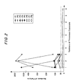
- Fig. 2 is a graph showing transition of particles under process conditions P1 to P8 described below.
- the lateral axis indicates the number of processed substrates subjected to the processes. Measurement of' particles is conducted by selecting an arbitrary number of multiple substrates from the substrates subjected to the process.
- a film to be deposited on an inner wall of the vacuum chamber 1 is limited only to ⁇ -Si film (an amorphous silicon film), and transition of particles is measured by changing the film thickness to 0.28 ⁇ m (P1), 0.55 ⁇ m (P2), 0.83 ⁇ m (P3), 1.1 ⁇ m (P4), and 1.65 ⁇ m (P5).
- P1 0.28 ⁇ m
- P2 0.55 ⁇ m
- P3 0.83 ⁇ m
- 1.1 ⁇ m P4
- 1.65 ⁇ m P5
- the particles tend to be reduced along with the increase in the deposited film thickness when changing the film thickness for depositing the ⁇ -Si film.
- transition of particles is measured by setting the deposited film thickness of the ⁇ -Si film to 1.1 ⁇ m, based on the foregoing results, and depositing 0.7 ⁇ m of a Si x N y film on the ⁇ -Si film.
- transition of particles is measured by depositing a Si x N y film, based on the result of P6, and increasing an amount of supply of N 2 gradually up to a predetermined flow rate when depositing the Si x N y film on the ⁇ -Si film.
- the level of particles becomes lower than the case of P6.
- transition of particles is measured by maintaining Ar plasma, based on the result of P7, after completion of a seasoning process for depositing the ⁇ -Si film and the Si x N y film until initiation of film formation on the substrate 5.
- the level of particle becomes even lower than the case of P7, and the number of particles becomes equal to or below 30 pieces in every session of the measurement.
- N 2 plasma is maintained in P1 to P6 unlike P7.
- plasma cleaning inside the vacuum chamber 1 is performed. This is executed periodically or once in every predetermined n pieces of the substrates (n is a natural number equal to or above 1), for example.
- a cleaning gas including predetermined flow rates of NF 3 , Ar (argon) and the like is supplied into the vacuum chamber 1, and plasma cleaning of the inner wall and the like of the vacuum chamber 1 is performed by converting, into a plasma state, the gas introduced into the vacuum chamber 1.
- etching is performed for the film attached to the inner wall and the like of the vacuum chamber 1 (Step S1).
- Step S2 a predetermined flow rate of SiH 4 is supplied into the vacuum chamber 1, and converted into a plasma state. Then a predetermined film thickness of the ⁇ -Si film is deposited on the inner wall and the like of the vacuum chamber 1, thereby coating the inner wall and the like of the vacuum chamber 1 (Step S2).
- N 2 is supplied in a gradually increasing manner up to a predetermined flow rate and similarly converted into a plasma state so as to perform coating by depositing a predetermined film thickness of the Si x N y film (the silicon nitride film) on the ⁇ -Si film (Step S3).
- a series of plasma cleaning and seasoning processes is completed.
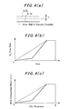
- the ⁇ -Si film and the Si x N y film are sequentially laminated on the inner wall and the like of the vacuum chamber 1 (see Fig. 4 (a) ), and N2 is supplied in a gradually increasing manner up to the predetermined flow rate at the time of deposition of the Si x N y film (see a graph in Fig. 4(b) ). Therefore, the ⁇ -Si film and the Si x N y film are sequentially laminated, while gently forming an interface between the ⁇ -Si film and the Si x N y film (in a state of not forming a clear interface). As a consequence, it is possible to render the seasoned Si x N y film hardly removable from the inner wall and the like of the vacuum chamber 1.
- a composition ratio (y/x) of N/Si in the Si x N y film is gradually increased in a thickness direction of the film thickness T thereof as shown in a graph in Fig. 4 (c) .
- This variation in the composition ratio in the thickness direction can be changed in response to a method of supplying N 2 .
- the composition ratio of N/Si in the Si x N y film when gradually increasing the amount of supply of N 2 up to the predetermined flow rate through multiple stages (two stages of the gradual increase including a gentle increase in the beginning and a more rapid increase thereafter), the composition ratio of N/Si in the Si x N y film also forms a similar profile as shown in a solid line of the graph in Fig. 4(c) .
- the composition ratio of N/Si in the Si x N y film also forms a similar profile as shown in a dotted line of the graph in Fig. 4(c) .
- a predetermined flow rate of Ar is supplied into the vacuum chamber 1 and Ar supplied into the vacuum chamber 1 is converted into a plasma state. Then the Ar plasma is maintained inside the vacuum chamber 1 (Step S4). Thereafter, in the state of maintaining the Ar plasma, the substrate 5 is conveyed and placed on the support table 4 of the vacuum chamber 1, and film formation of the silicon nitride film on the substrate 5 is carried out as usual. After carrying out the film formation on n pieces of the substrates 5, the process returns to Step S1 and the series of the plasma cleaning and seasoning processes is started again (Step S5). Note that, it is also possible to use other rare gases instead of Ar in this step.
- the physical characteristics of the silicon nitride film of being apt to be peeled off and to become particles are changed by executing the seasoning method for a film-forming apparatus (the series of the plasma cleaning, seasoning processes and the like) in accordance with the above-described procedures.
- the seasoning method for a film-forming apparatus the series of the plasma cleaning, seasoning processes and the like
- particles are usually charged negatively in the plasma so that the Ar plasma traps more particles by maintaining the Ar plasma that has more positive plasma potential than the N2 plasma, thereby reducing more particles as a consequence.
- seasoning method for a film-forming apparatus is suitable for a silicon nitride film having high stress of the film itself and having poor adhesion, it is also applicable to other films having similar properties to the silicon nitride film.
Landscapes
- Chemical & Material Sciences (AREA)
- Engineering & Computer Science (AREA)
- Metallurgy (AREA)
- Chemical Kinetics & Catalysis (AREA)
- Materials Engineering (AREA)
- Mechanical Engineering (AREA)
- General Chemical & Material Sciences (AREA)
- Organic Chemistry (AREA)
- Health & Medical Sciences (AREA)
- Epidemiology (AREA)
- Public Health (AREA)
- Physics & Mathematics (AREA)
- Plasma & Fusion (AREA)
- Analytical Chemistry (AREA)
- Chemical Vapour Deposition (AREA)
Abstract
A seasoning method for a film-forming apparatus configured to form a silicon nitride film on a substrate placed in a process chamber. The method is conducted for reducing particles in the apparatus. The method comprises executing the plasma cleaning of the process chamber to remove a film deposited on the inner wall thereof (step S1), subsequently depositing an amorphous silicon film (step S2), depositing thereon a silicon nitride film in which the nitrogen content gradually increases in the thickness direction (step S3), and keeping the inside of the process chamber being filled with a rare-gas plasma until film formation on the substrate is initiated (step S4).
Description
- The present invention relates to a seasoning method for a film-forming apparatus, which is suitable for a plasma CVD apparatus or the like configured to form films constituting a semiconductor device, for example.
- In order to form films that constitute a semiconductor device in a semiconductor process, films are formed on a substrate by use of a film-forming apparatus such as a plasma CVD apparatus. At this time, films to be formed are attached not only onto the substrate but also onto an inner wall of a processing chamber of the film-forming apparatus. The films attached to the inner wall of the processing chamber are further deposited thereon each time films are formed on the substrate, and are peeled off if they are left intact and may cause particles. Accordingly, plasma cleaning is periodically performed to remove the unnecessary films attached to the inner wall.
Moreover, in order to suppress contaminants and to stabilize the process, a film formation process for a predetermined amount is usually performed with no substrate while formed under the same conditions as film formation on the substrate (seasoning).
Patent Document 1:JP-A 11-16845 - Seasoning is necessary for stabilizing the process. However, in the case of a silicon nitride film, the film itself has high stress and low adhesion to the inner wall of the processing chamber. Therefore, the film is apt to be peeled off from the inner wall of the processing chamber, and to become particles, thereby leading to a problem that the generation of particles cannot be reduced.
- The present invention has been made in view of the foregoing problem and aims at providing a seasoning method for a film-forming apparatus configured to reduce the generation of particles.
- A seasoning method for a film-forming apparatus described in a first invention to solve the above problem is a seasoning method for a film-forming apparatus configured to form a silicon nitride film on a substrate placed in a processing chamber, comprising: supplying a cleaning gas into the processing chamber, and etching the silicon nitride film attached to an inner wall of the processing chamber while converting the cleaning gas into a plasma state; supplying a silicon-containing gas into the processing chamber, and depositing an amorphous silicon film on the inner wall of the processing chamber while converting the silicon-containing gas into a plasma state; supplying the silicon-containing gas into the processing chamber, while supplying a nitrogen-containing gas in a gradually increasing manner up to a predetermined flow rate, and thus depositing, on the amorphous silicon film, a silicon nitride film with the nitrogen content gradually increasing in a thickness direction, while converting the silicon-containing gas and the nitrogen-containing gas into a plasma state; and supplying a rare gas into the processing chamber, and maintaining a plasma state of the rare gas until film formation of the silicon nitride film on the substrate is initiated.
- A seasoning method for a film-forming apparatus described in a second invention to solve the above problem is the seasoning method for a film-forming apparatus according to the first invention, wherein the nitrogen-containing gas is supplied in a gradually increasing manner up to the predetermined flow rate gently in the beginning and more rapidly thereafter when depositing the silicon nitride film on the amorphous silicon film.
- According to the present invention, the amorphous silicon film is deposited after performing plasma cleaning (etching) of the film attached to the inner wall of the processing chamber, and the silicon nitride film in which the nitrogen content is gradually increased in the thickness direction is deposited thereon. Moreover, the inside of the processing chamber is maintained with the rare gas plasma until film formation on the substrate is initiated. Therefore, it is possible to reduce particles at the time of film formation on the substrate.
-
- [
Figure 1] Fig. 1 is a schematic configuration diagram showing an example of an embodiment of a film-forming apparatus in the present invention. - [
Figure 2] Fig. 2 is a graph showing transition of particles under process conditions P1 to P8. - [
Figure 3] Fig. 3 is a flowchart explaining a seasoning method for a film-forming apparatus according to the present invention. - [
Figure 4] Figs. 4(a) to 4(c) are views explaining a deposition state of each film and a supply state of a nitrogen flow rate in the seasoning method for a film-forming apparatus according to the present invention. -
- 1
- VACUUM CHAMBER
- 2
- PROCESSING CHAMBER
- 3
- CEILING PLATE
- 4
- SUPPORT TABLE
- 5
- SUBSTRATE
- 7
- ANTENNAS
- 8
- MATCHING BOX
- 9
- HIGH-FREQUENCY POWER SOURCE
- 10a, 10b
- GAS NOZZLES
- 11
- EXHAUST PORT
- 12
- ANTENNA
- 13
- MATCHING BOX
- 14
- ALTERNATING-CURRENT POWER SOURCE
- A seasoning method for a film-forming apparatus according to the present invention will be described in detail by using
Fig. 1 to Fig. 4(c) . -
Fig. 1 is a schematic configuration diagram showing an example of an embodiment of a film-forming apparatus according to the present invention.
As shown inFig. 1 , in the film-forming apparatus according to the present invention, the inside of acylindrical vacuum chamber 1 made of aluminum is configured to serve as a processing chamber 2 (a treatment vessel), and adiscoid ceiling plate 3 made of a ceramic constituting an electromagnetic wave transmissive window is disposed on an upper opening portion of thevacuum chamber 1 so as to occlude the opening portion. Meanwhile, a support table 4 is provided in the lower part of thevacuum chamber 1 and asubstrate 5 such as a semiconductor is placed on an upper surface of the support table 4. - Multiple high-
frequency antennas 7 made of circular rings, for example, are disposed on an upper part of theceiling plate 3, and a high-frequency power source 9 for plasma generation is connected to one of the high-frequency antennas 7 through a matchingbox 8 configured to perform impedance matching. - Moreover, the
vacuum chamber 1 is provided withgas nozzles processing chamber 2, and is also provided with anexhaust port 11. Theexhaust port 11 is connected to an unillustrated vacuum pumping system, and the inside of theprocessing chamber 2 is controlled to a desired pressure by using this vacuum pumping system. - The support table 4 for supporting the
substrate 5 is provided with anantenna 12. An alternating-current power source 14 for biasing is connected to thisantenna 12 through a matchingbox 13 configured to perform impedance matching. Theantenna 12 functions as a bias electrode for applying bias power to thesubstrate 5. - In the film-forming apparatus having the above-described configuration, by supplying high-frequency power from the high-
frequency power source 9 to the high-frequency antenna 7, an electromagnetic wave from the high-frequency antenna 7 passes through theceiling plate 3, and is made incident on theprocessing chamber 2. The gases introduced into theprocessing chamber 2 through thegas nozzles substrate 5 by using the generated plasma. - For instance, in the case of forming a SixNy film (silicon nitride film) on the
substrate 5, a plasma process is executed by supplying SiH4 (silane) or the like, for example, as a raw material gas, whereas supplying NH3 (ammonia), N2 (nitrogen) or the like, for example, as a nitriding gas. Thus, the silicon nitride film having a desired film thickness is formed on eachsubstrate 5 one by one. Then, plasma cleaning is usually executed periodically by use of NF3 (nitrogen trifluoride).
Thereafter, seasoning is performed under the same conditions as film formation on the substrate for the purpose of process stabilization. - However, as described previously, the SixNy film has large stress of the film itself and poor adhesion to the
vacuum chamber 1. Accordingly, it has been difficult to reduce particles to a desired level. Therefore, the inventors of the present invention acquired the most suitable seasoning method for reducing particles, based on the knowledge shown inFig. 2 and so forth. Note thatFig. 2 is a graph showing transition of particles under process conditions P1 to P8 described below. Meanwhile, the lateral axis indicates the number of processed substrates subjected to the processes. Measurement of' particles is conducted by selecting an arbitrary number of multiple substrates from the substrates subjected to the process. - First, a film to be deposited on an inner wall of the
vacuum chamber 1 is limited only to α-Si film (an amorphous silicon film), and transition of particles is measured by changing the film thickness to 0.28 µm (P1), 0.55 µm (P2), 0.83 µm (P3), 1.1 µm (P4), and 1.65 µm (P5). As apparent from the graph inFig. 2 , the particles tend to be reduced along with the increase in the deposited film thickness when changing the film thickness for depositing the α-Si film. However, there is not a large difference between 1.1 µm (P4) and the 1.65 µm (P5), and the most suitable deposited film thickness of the α-Si film turns out to be around 1.1 µm. - Therefore, in the process condition of P6, transition of particles is measured by setting the deposited film thickness of the α-Si film to 1.1 µm, based on the foregoing results, and depositing 0.7 µm of a SixNy film on the α-Si film. In this case, there is not a large difference from the cases of P4 and P5 as shown in the graph in
Fig. 2 . - Next, in the process condition of P7, transition of particles is measured by depositing a SixNy film, based on the result of P6, and increasing an amount of supply of N2 gradually up to a predetermined flow rate when depositing the SixNy film on the α-Si film. In this case, as shown in the graph in
Fig. 2 , the level of particles becomes lower than the case of P6. - Then in the process condition of P8, transition of particles is measured by maintaining Ar plasma, based on the result of P7, after completion of a seasoning process for depositing the α-Si film and the SixNy film until initiation of film formation on the
substrate 5. In this case, as shown in the graph inFig. 2 , the level of particle becomes even lower than the case of P7, and the number of particles becomes equal to or below 30 pieces in every session of the measurement. Note that N2 plasma is maintained in P1 to P6 unlike P7. - Here, a seasoning method for a film-forming apparatus according to the present invention obtained based on the above-described knowledge will be described by using
Fig. 3 to Fig. 4(c) . - First, plasma cleaning inside the
vacuum chamber 1 is performed. This is executed periodically or once in every predetermined n pieces of the substrates (n is a natural number equal to or above 1), for example. At the time of this plasma cleaning, a cleaning gas including predetermined flow rates of NF3, Ar (argon) and the like is supplied into thevacuum chamber 1, and plasma cleaning of the inner wall and the like of thevacuum chamber 1 is performed by converting, into a plasma state, the gas introduced into thevacuum chamber 1. Thus, etching is performed for the film attached to the inner wall and the like of the vacuum chamber 1 (Step S1). - Next, a predetermined flow rate of SiH4 is supplied into the
vacuum chamber 1, and converted into a plasma state. Then a predetermined film thickness of the α-Si film is deposited on the inner wall and the like of thevacuum chamber 1, thereby coating the inner wall and the like of the vacuum chamber 1 (Step S2). - Next, N2 is supplied in a gradually increasing manner up to a predetermined flow rate and similarly converted into a plasma state so as to perform coating by depositing a predetermined film thickness of the SixNy film (the silicon nitride film) on the α-Si film (Step S3). Thus, a series of plasma cleaning and seasoning processes is completed.
- According to the above-described procedures, the α-Si film and the SixNy film are sequentially laminated on the inner wall and the like of the vacuum chamber 1 (see
Fig. 4 (a) ), and N2 is supplied in a gradually increasing manner up to the predetermined flow rate at the time of deposition of the SixNy film (see a graph inFig. 4(b) ). Therefore, the α-Si film and the SixNy film are sequentially laminated, while gently forming an interface between the α-Si film and the SixNy film (in a state of not forming a clear interface). As a consequence, it is possible to render the seasoned SixNy film hardly removable from the inner wall and the like of thevacuum chamber 1. - At this time, a composition ratio (y/x) of N/Si in the SixNy film is gradually increased in a thickness direction of the film thickness T thereof as shown in a graph in
Fig. 4 (c) . This variation in the composition ratio in the thickness direction can be changed in response to a method of supplying N2. For example, as shown in a solid line of the graph inFig. 4(b) , when gradually increasing the amount of supply of N2 up to the predetermined flow rate through multiple stages (two stages of the gradual increase including a gentle increase in the beginning and a more rapid increase thereafter), the composition ratio of N/Si in the SixNy film also forms a similar profile as shown in a solid line of the graph inFig. 4(c) . Meanwhile, as shown in a dotted line of the graph inFig. 4 (b) , when gradually increasing the amount of supply of N2 up to the predetermined flow rate in one stage (at a constant inclination), the composition ratio of N/Si in the SixNy film also forms a similar profile as shown in a dotted line of the graph inFig. 4(c) . - After the above-described series of processes, a predetermined flow rate of Ar is supplied into the
vacuum chamber 1 and Ar supplied into thevacuum chamber 1 is converted into a plasma state. Then the Ar plasma is maintained inside the vacuum chamber 1 (Step S4). Thereafter, in the state of maintaining the Ar plasma, thesubstrate 5 is conveyed and placed on the support table 4 of thevacuum chamber 1, and film formation of the silicon nitride film on thesubstrate 5 is carried out as usual. After carrying out the film formation on n pieces of thesubstrates 5, the process returns to Step S1 and the series of the plasma cleaning and seasoning processes is started again (Step S5). Note that, it is also possible to use other rare gases instead of Ar in this step. - Concerning the plasma generated inside the
vacuum chamber 1, it is possible to stop generation thereof (stop incidence of the electromagnetic wave) in each of the above-described steps. However, it is also possible to maintain the plasma state during the series of steps, namely, during the plasma cleaning, seasoning, and Ar plasma processes. - In the present invention, the physical characteristics of the silicon nitride film of being apt to be peeled off and to become particles are changed by executing the seasoning method for a film-forming apparatus (the series of the plasma cleaning, seasoning processes and the like) in accordance with the above-described procedures. As a consequence, it is possible to render the silicon nitride film less removable, to reduce an amount of generation of particles, and thereby to stabilize the process.
- This is presumably because the stress of the silicon nitride film itself is relaxed and adhesion thereof is also improved by laminating the silicon nitride film having the nitrogen content gradually increased in the thickness direction on the inner wall and the like of the
vacuum chamber 1 through the α-Si film, and the silicon nitride film becomes less removable as a consequence. In particular, it is presumably more desirable to form the interface between the α-Si film and the silicon nitride film gently by means of gradually increasing the amount of supply of N2 gently in the beginning and then more rapidly thereafter. - Moreover, in terms of maintaining the Ar plasma in the course of conveying the
substrate 5, particles are usually charged negatively in the plasma so that the Ar plasma traps more particles by maintaining the Ar plasma that has more positive plasma potential than the N2 plasma, thereby reducing more particles as a consequence. - Although the seasoning method for a film-forming apparatus according to the present invention is suitable for a silicon nitride film having high stress of the film itself and having poor adhesion, it is also applicable to other films having similar properties to the silicon nitride film.
Claims (2)
- A seasoning method for a film-forming apparatus configured to form a silicon nitride film on a substrate placed in a processing chamber, comprising:supplying a cleaning gas into the processing chamber, and etching the silicon nitride film attached to an inner wall of the processing chamber while converting the cleaning gas into a plasma state;supplying a silicon-containing gas into the processing chamber, and depositing an amorphous silicon film on the inner wall of the processing chamber while converting the silicon-containing gas into a plasma state;supplying the silicon-containing gas into the processing chamber, while supplying a nitrogen-containing gas in a gradually increasing manner up to a predetermined flow rate, and thus depositing, on the amorphous silicon film, a silicon nitride film with the nitrogen content gradually increasing in a thickness direction, while converting the silicon-containing gas and the nitrogen-containing gas into a plasma state; andsupplying a rare gas into the processing chamber and maintaining a plasma state of the rare gas until film formation of the silicon nitride film on the substrate is initiated.
- The seasoning method for a film-forming apparatus according to claim 1,
wherein the nitrogen-containing gas is supplied in a gradually increasing manner up to the predetermined flow rate gently in the beginning and more rapidly thereafter when depositing the silicon nitride film on the amorphous silicon film.
Applications Claiming Priority (2)
| Application Number | Priority Date | Filing Date | Title |
|---|---|---|---|
| JP2006065415A JP4476232B2 (en) | 2006-03-10 | 2006-03-10 | Seasoning method for film forming apparatus |
| PCT/JP2007/052921 WO2007105412A1 (en) | 2006-03-10 | 2007-02-19 | Method of seasoning film-forming apparatus |
Publications (1)
| Publication Number | Publication Date |
|---|---|
| EP1995770A1 true EP1995770A1 (en) | 2008-11-26 |
Family
ID=38509250
Family Applications (1)
| Application Number | Title | Priority Date | Filing Date |
|---|---|---|---|
| EP07714447A Withdrawn EP1995770A1 (en) | 2006-03-10 | 2007-02-19 | Method of seasoning film-forming apparatus |
Country Status (6)
| Country | Link |
|---|---|
| US (1) | US8337960B2 (en) |
| EP (1) | EP1995770A1 (en) |
| JP (1) | JP4476232B2 (en) |
| KR (1) | KR101004975B1 (en) |
| TW (1) | TW200741869A (en) |
| WO (1) | WO2007105412A1 (en) |
Families Citing this family (23)
| Publication number | Priority date | Publication date | Assignee | Title |
|---|---|---|---|---|
| US7659184B2 (en) * | 2008-02-25 | 2010-02-09 | Applied Materials, Inc. | Plasma immersion ion implantation process with chamber seasoning and seasoning layer plasma discharging for wafer dechucking |
| CN102405511B (en) * | 2009-04-20 | 2014-06-11 | 应用材料公司 | Method for enhanced scavenging of residual fluorine radicals using silicon coatings on process chamber walls |
| JP5275188B2 (en) * | 2009-09-18 | 2013-08-28 | 東京エレクトロン株式会社 | Method for determining whether to start processing and storage medium |
| US20110117680A1 (en) * | 2009-11-17 | 2011-05-19 | Applied Materials, Inc. | Inline detection of substrate positioning during processing |
| US8999847B2 (en) | 2010-08-16 | 2015-04-07 | Applied Materials, Inc. | a-Si seasoning effect to improve SiN run-to-run uniformity |
| JP5772508B2 (en) * | 2011-10-27 | 2015-09-02 | 東京エレクトロン株式会社 | Film forming apparatus and operation method thereof |
| JP5807511B2 (en) * | 2011-10-27 | 2015-11-10 | 東京エレクトロン株式会社 | Film forming apparatus and operation method thereof |
| CN104099582B (en) * | 2013-04-15 | 2016-10-19 | 中芯国际集成电路制造(上海)有限公司 | A kind of reduce the method for granule in boiler tube |
| CN104250727A (en) * | 2013-06-26 | 2014-12-31 | 中芯国际集成电路制造(上海)有限公司 | After-maintenance recovering method of chemical vapor deposition equipment |
| CN104250726B (en) * | 2013-06-26 | 2017-05-24 | 中芯国际集成电路制造(上海)有限公司 | Quartz tube protection method |
| EP2821104A1 (en) | 2013-07-05 | 2015-01-07 | Laboratoire Biodim | Inhibitors of viral replication, their process of preparation and their therapeutical uses |
| JP2015070233A (en) * | 2013-09-30 | 2015-04-13 | 株式会社東芝 | Manufacturing method of semiconductor device |
| US9745658B2 (en) | 2013-11-25 | 2017-08-29 | Lam Research Corporation | Chamber undercoat preparation method for low temperature ALD films |
| US9548188B2 (en) | 2014-07-30 | 2017-01-17 | Lam Research Corporation | Method of conditioning vacuum chamber of semiconductor substrate processing apparatus |
| US9828672B2 (en) | 2015-03-26 | 2017-11-28 | Lam Research Corporation | Minimizing radical recombination using ALD silicon oxide surface coating with intermittent restoration plasma |
| US10023956B2 (en) | 2015-04-09 | 2018-07-17 | Lam Research Corporation | Eliminating first wafer metal contamination effect in high density plasma chemical vapor deposition systems |
| US10211099B2 (en) | 2016-12-19 | 2019-02-19 | Lam Research Corporation | Chamber conditioning for remote plasma process |
| JP2021506126A (en) | 2017-12-07 | 2021-02-18 | ラム リサーチ コーポレーションLam Research Corporation | Oxidation resistant protective layer in chamber adjustment |
| US10760158B2 (en) | 2017-12-15 | 2020-09-01 | Lam Research Corporation | Ex situ coating of chamber components for semiconductor processing |
| JP7474700B2 (en) * | 2018-03-01 | 2024-04-25 | アプライド マテリアルズ インコーポレイテッド | Systems and methods for forming metal hardmasks in device manufacturing - Patents.com |
| KR20250110938A (en) | 2018-10-19 | 2025-07-21 | 램 리써치 코포레이션 | In situ protective coating of chamber components for semiconductor processing |
| TW202122909A (en) * | 2019-10-25 | 2021-06-16 | 美商應用材料股份有限公司 | Extreme ultraviolet mask blank defect reduction methods |
| US11646216B2 (en) * | 2020-10-16 | 2023-05-09 | Applied Materials, Inc. | Systems and methods of seasoning electrostatic chucks with dielectric seasoning films |
Family Cites Families (27)
| Publication number | Priority date | Publication date | Assignee | Title |
|---|---|---|---|---|
| US5324360A (en) * | 1991-05-21 | 1994-06-28 | Canon Kabushiki Kaisha | Method for producing non-monocrystalline semiconductor device and apparatus therefor |
| JPH0831752A (en) * | 1994-07-15 | 1996-02-02 | Toshiba Corp | Method of cleaning reaction chamber of CVD apparatus and method of coating |
| JP3471082B2 (en) * | 1994-07-15 | 2003-11-25 | 株式会社東芝 | Coating method for reaction chamber of CVD apparatus |
| US5563096A (en) * | 1995-11-20 | 1996-10-08 | Digital Equipment Corporation | Semiconductor device fabrication with planar gate interconnect surface |
| GB2311299B (en) * | 1996-03-18 | 2000-03-29 | Hyundai Electronics Ind | Inductively coupled plasma chemical vapor deposition technology |
| US5821603A (en) * | 1996-05-29 | 1998-10-13 | Microunity Systems Engineering, Inc. | Method for depositing double nitride layer in semiconductor processing |
| JP3311244B2 (en) * | 1996-07-15 | 2002-08-05 | 株式会社東芝 | Basic cell library and method of forming the same |
| US6184158B1 (en) * | 1996-12-23 | 2001-02-06 | Lam Research Corporation | Inductively coupled plasma CVD |
| US5896870A (en) * | 1997-03-11 | 1999-04-27 | International Business Machines Corporation | Method of removing slurry particles |
| US20030143410A1 (en) * | 1997-03-24 | 2003-07-31 | Applied Materials, Inc. | Method for reduction of contaminants in amorphous-silicon film |
| TW460943B (en) | 1997-06-11 | 2001-10-21 | Applied Materials Inc | Reduction of mobile ion and metal contamination in HDP-CVD chambers using chamber seasoning film depositions |
| US6534007B1 (en) | 1997-08-01 | 2003-03-18 | Applied Komatsu Technology, Inc. | Method and apparatus for detecting the endpoint of a chamber cleaning |
| JP3112880B2 (en) | 1998-02-06 | 2000-11-27 | 鹿児島日本電気株式会社 | Cleaning method for CVD equipment |
| US5950090A (en) * | 1998-11-16 | 1999-09-07 | United Microelectronics Corp. | Method for fabricating a metal-oxide semiconductor transistor |
| KR100378180B1 (en) * | 2000-05-22 | 2003-03-29 | 삼성전자주식회사 | Slurry for chemical mechanical polishing process and method of manufacturing semiconductor device using the same |
| US6372605B1 (en) * | 2000-06-26 | 2002-04-16 | Agere Systems Guardian Corp. | Additional etching to decrease polishing time for shallow-trench isolation in semiconductor processing |
| KR100375102B1 (en) * | 2000-10-18 | 2003-03-08 | 삼성전자주식회사 | Method for CVD and apparatus for performing the same in semiconductor device processing |
| US6664190B2 (en) * | 2001-09-14 | 2003-12-16 | Chartered Semiconductor Manufacturing Ltd. | Pre STI-CMP planarization scheme |
| JP2003277734A (en) * | 2001-12-31 | 2003-10-02 | Hynix Semiconductor Inc | CMP slurry for metal and method for forming metal wiring contact plug of semiconductor device using the same |
| JP4212861B2 (en) * | 2002-09-30 | 2009-01-21 | 株式会社フジミインコーポレーテッド | Polishing composition and silicon wafer polishing method using the same, and rinsing composition and silicon wafer rinsing method using the same |
| US7244474B2 (en) * | 2004-03-26 | 2007-07-17 | Applied Materials, Inc. | Chemical vapor deposition plasma process using an ion shower grid |
| US7195535B1 (en) * | 2004-07-22 | 2007-03-27 | Applied Materials, Inc. | Metrology for chemical mechanical polishing |
| US20060130891A1 (en) * | 2004-10-29 | 2006-06-22 | Carlson David E | Back-contact photovoltaic cells |
| US7166506B2 (en) * | 2004-12-17 | 2007-01-23 | Intel Corporation | Poly open polish process |
| TWI372108B (en) * | 2005-04-06 | 2012-09-11 | Rohm & Haas Elect Mat | Method for forming a porous reaction injection molded chemical mechanical polishing pad |
| US20090056743A1 (en) * | 2007-08-31 | 2009-03-05 | Soo Young Choi | Method of cleaning plasma enhanced chemical vapor deposition chamber |
| US7838366B2 (en) * | 2008-04-11 | 2010-11-23 | United Microelectronics Corp. | Method for fabricating a metal gate structure |
-
2006
- 2006-03-10 JP JP2006065415A patent/JP4476232B2/en not_active Expired - Fee Related
-
2007
- 2007-02-19 EP EP07714447A patent/EP1995770A1/en not_active Withdrawn
- 2007-02-19 US US12/282,475 patent/US8337960B2/en not_active Expired - Fee Related
- 2007-02-19 WO PCT/JP2007/052921 patent/WO2007105412A1/en not_active Ceased
- 2007-02-19 KR KR1020087022176A patent/KR101004975B1/en not_active Expired - Fee Related
- 2007-03-02 TW TW096107225A patent/TW200741869A/en not_active IP Right Cessation
Non-Patent Citations (1)
| Title |
|---|
| See references of WO2007105412A1 * |
Also Published As
| Publication number | Publication date |
|---|---|
| TWI351062B (en) | 2011-10-21 |
| US20090242511A1 (en) | 2009-10-01 |
| WO2007105412A1 (en) | 2007-09-20 |
| KR20080103068A (en) | 2008-11-26 |
| JP4476232B2 (en) | 2010-06-09 |
| TW200741869A (en) | 2007-11-01 |
| JP2007242996A (en) | 2007-09-20 |
| US8337960B2 (en) | 2012-12-25 |
| KR101004975B1 (en) | 2011-01-04 |
Similar Documents
| Publication | Publication Date | Title |
|---|---|---|
| US8337960B2 (en) | Seasoning method for film-forming apparatus | |
| EP0630990B1 (en) | Method of limiting sticking of body to a susceptor in a deposition treatment | |
| KR101379089B1 (en) | Metal hard mask fabrication | |
| JP3725100B2 (en) | Deposition method | |
| US8637410B2 (en) | Method for metal deposition using hydrogen plasma | |
| EP1672093B1 (en) | Film-forming apparatus and film-forming method | |
| EP0630989B1 (en) | Method of plasma chemical vapor deposition of layer with improved interface | |
| US9551070B2 (en) | In-situ corrosion resistant substrate support coating | |
| US5510297A (en) | Process for uniform deposition of tungsten silicide on semiconductor wafers by treatment of susceptor having aluminum nitride surface thereon with tungsten silicide after cleaning of susceptor | |
| KR102046163B1 (en) | Method of fabricating semiconductor device | |
| EP3617342B1 (en) | Method of depositing silicon nitride | |
| CN114867890A (en) | Initial modulation for plasma deposition | |
| JPH06252059A (en) | Method and apparatus for forming film | |
| WO2019169298A1 (en) | Systems and methods of formation of a metal hardmask in device fabrication | |
| WO2026016919A1 (en) | Method for forming protective film, protective film, and semiconductor process apparatus | |
| JPH0456770A (en) | Method for cleaning plasma cvd device | |
| US7972961B2 (en) | Purge step-controlled sequence of processing semiconductor wafers | |
| CN117721441B (en) | High-stress silicon nitride film and forming method thereof | |
| KR20180059609A (en) | Apparatus For Depositing Thin Film, System Having The Same And Method of Depositing The Thin Film | |
| JP3178431B2 (en) | Cleaning method for plasma CVD apparatus | |
| CN116635977A (en) | Tensile nitride deposition systems and methods | |
| KR20210066080A (en) | Seasoning method of substrate processing apparatus and method of processing the substrate | |
| CN116759297B (en) | Method for reducing wafer surface temperature in continuous preparation of low-temperature silicon nitride film | |
| TWI856541B (en) | Silicon-containing layers with reduced hydrogen content and processes of making them | |
| WO2026107094A1 (en) | Controlling fluorine diffusion in pecvd silicon nitride process |
Legal Events
| Date | Code | Title | Description |
|---|---|---|---|
| PUAI | Public reference made under article 153(3) epc to a published international application that has entered the european phase |
Free format text: ORIGINAL CODE: 0009012 |
|
| 17P | Request for examination filed |
Effective date: 20080904 |
|
| AK | Designated contracting states |
Kind code of ref document: A1 Designated state(s): AT BE BG CH CY CZ DE DK EE ES FI FR GB GR HU IE IS IT LI LT LU LV MC NL PL PT RO SE SI SK TR |
|
| DAX | Request for extension of the european patent (deleted) | ||
| STAA | Information on the status of an ep patent application or granted ep patent |
Free format text: STATUS: THE APPLICATION HAS BEEN WITHDRAWN |
|
| 18W | Application withdrawn |
Effective date: 20141103 |