EP1995615A1 - Photo/electrical mixed mounting substrate and method for producing the same - Google Patents
Photo/electrical mixed mounting substrate and method for producing the same Download PDFInfo
- Publication number
- EP1995615A1 EP1995615A1 EP07714516A EP07714516A EP1995615A1 EP 1995615 A1 EP1995615 A1 EP 1995615A1 EP 07714516 A EP07714516 A EP 07714516A EP 07714516 A EP07714516 A EP 07714516A EP 1995615 A1 EP1995615 A1 EP 1995615A1
- Authority
- EP
- European Patent Office
- Prior art keywords
- optical
- hole
- circuit board
- electrical circuit
- filling
- Prior art date
- Legal status (The legal status is an assumption and is not a legal conclusion. Google has not performed a legal analysis and makes no representation as to the accuracy of the status listed.)
- Withdrawn
Links
- 239000000758 substrate Substances 0.000 title claims description 59
- 238000004519 manufacturing process Methods 0.000 title claims description 34
- 230000003287 optical effect Effects 0.000 claims abstract description 224
- 239000000463 material Substances 0.000 claims abstract description 139
- 238000000034 method Methods 0.000 claims description 24
- 230000002093 peripheral effect Effects 0.000 claims description 22
- 238000009429 electrical wiring Methods 0.000 claims description 9
- 230000005540 biological transmission Effects 0.000 claims description 3
- 238000002834 transmittance Methods 0.000 claims description 3
- 229920005989 resin Polymers 0.000 abstract description 17
- 239000011347 resin Substances 0.000 abstract description 17
- 238000000016 photochemical curing Methods 0.000 abstract description 15
- 239000010410 layer Substances 0.000 description 109
- 238000006243 chemical reaction Methods 0.000 description 19
- 239000002184 metal Substances 0.000 description 14
- 229910052751 metal Inorganic materials 0.000 description 14
- 239000011229 interlayer Substances 0.000 description 8
- 239000007788 liquid Substances 0.000 description 8
- 238000001723 curing Methods 0.000 description 7
- 229920001187 thermosetting polymer Polymers 0.000 description 4
- 238000005516 engineering process Methods 0.000 description 3
- 239000003822 epoxy resin Substances 0.000 description 3
- 238000000059 patterning Methods 0.000 description 3
- 230000000149 penetrating effect Effects 0.000 description 3
- 229920000647 polyepoxide Polymers 0.000 description 3
- 238000004891 communication Methods 0.000 description 2
- 239000000470 constituent Substances 0.000 description 2
- 239000000945 filler Substances 0.000 description 2
- 238000000227 grinding Methods 0.000 description 2
- 229910010272 inorganic material Inorganic materials 0.000 description 2
- 239000011147 inorganic material Substances 0.000 description 2
- 239000011368 organic material Substances 0.000 description 2
- 239000004065 semiconductor Substances 0.000 description 2
- 229910000679 solder Inorganic materials 0.000 description 2
- 229920000178 Acrylic resin Polymers 0.000 description 1
- 239000004925 Acrylic resin Substances 0.000 description 1
- RYGMFSIKBFXOCR-UHFFFAOYSA-N Copper Chemical compound [Cu] RYGMFSIKBFXOCR-UHFFFAOYSA-N 0.000 description 1
- 239000004593 Epoxy Substances 0.000 description 1
- XUIMIQQOPSSXEZ-UHFFFAOYSA-N Silicon Chemical compound [Si] XUIMIQQOPSSXEZ-UHFFFAOYSA-N 0.000 description 1
- 239000003990 capacitor Substances 0.000 description 1
- 239000000919 ceramic Substances 0.000 description 1
- 239000011529 conductive interlayer Substances 0.000 description 1
- 229910052802 copper Inorganic materials 0.000 description 1
- 239000010949 copper Substances 0.000 description 1
- 230000008021 deposition Effects 0.000 description 1
- 230000000694 effects Effects 0.000 description 1
- 238000007772 electroless plating Methods 0.000 description 1
- 238000010894 electron beam technology Methods 0.000 description 1
- 239000011521 glass Substances 0.000 description 1
- 238000010438 heat treatment Methods 0.000 description 1
- 230000002452 interceptive effect Effects 0.000 description 1
- 238000012986 modification Methods 0.000 description 1
- 230000004048 modification Effects 0.000 description 1
- 239000013307 optical fiber Substances 0.000 description 1
- 239000002245 particle Substances 0.000 description 1
- 238000005498 polishing Methods 0.000 description 1
- 239000000843 powder Substances 0.000 description 1
- 229910052710 silicon Inorganic materials 0.000 description 1
- 239000010703 silicon Substances 0.000 description 1
- 230000008961 swelling Effects 0.000 description 1
- 238000005406 washing Methods 0.000 description 1
Images





Classifications
-
- G—PHYSICS
- G02—OPTICS
- G02B—OPTICAL ELEMENTS, SYSTEMS OR APPARATUS
- G02B6/00—Light guides; Structural details of arrangements comprising light guides and other optical elements, e.g. couplings
- G02B6/10—Light guides; Structural details of arrangements comprising light guides and other optical elements, e.g. couplings of the optical waveguide type
- G02B6/12—Light guides; Structural details of arrangements comprising light guides and other optical elements, e.g. couplings of the optical waveguide type of the integrated circuit kind
- G02B6/13—Integrated optical circuits characterised by the manufacturing method
-
- G—PHYSICS
- G02—OPTICS
- G02B—OPTICAL ELEMENTS, SYSTEMS OR APPARATUS
- G02B6/00—Light guides; Structural details of arrangements comprising light guides and other optical elements, e.g. couplings
- G02B6/10—Light guides; Structural details of arrangements comprising light guides and other optical elements, e.g. couplings of the optical waveguide type
- G02B6/12—Light guides; Structural details of arrangements comprising light guides and other optical elements, e.g. couplings of the optical waveguide type of the integrated circuit kind
- G02B6/12004—Combinations of two or more optical elements
-
- G—PHYSICS
- G02—OPTICS
- G02B—OPTICAL ELEMENTS, SYSTEMS OR APPARATUS
- G02B6/00—Light guides; Structural details of arrangements comprising light guides and other optical elements, e.g. couplings
- G02B6/10—Light guides; Structural details of arrangements comprising light guides and other optical elements, e.g. couplings of the optical waveguide type
- G02B6/12—Light guides; Structural details of arrangements comprising light guides and other optical elements, e.g. couplings of the optical waveguide type of the integrated circuit kind
- G02B6/122—Basic optical elements, e.g. light-guiding paths
-
- G—PHYSICS
- G02—OPTICS
- G02B—OPTICAL ELEMENTS, SYSTEMS OR APPARATUS
- G02B6/00—Light guides; Structural details of arrangements comprising light guides and other optical elements, e.g. couplings
- G02B6/24—Coupling light guides
- G02B6/42—Coupling light guides with opto-electronic elements
- G02B6/43—Arrangements comprising a plurality of opto-electronic elements and associated optical interconnections
-
- G—PHYSICS
- G02—OPTICS
- G02B—OPTICAL ELEMENTS, SYSTEMS OR APPARATUS
- G02B7/00—Mountings, adjusting means, or light-tight connections, for optical elements
- G02B7/02—Mountings, adjusting means, or light-tight connections, for optical elements for lenses
- G02B7/022—Mountings, adjusting means, or light-tight connections, for optical elements for lenses lens and mount having complementary engagement means, e.g. screw/thread
-
- H—ELECTRICITY
- H05—ELECTRIC TECHNIQUES NOT OTHERWISE PROVIDED FOR
- H05K—PRINTED CIRCUITS; CASINGS OR CONSTRUCTIONAL DETAILS OF ELECTRIC APPARATUS; MANUFACTURE OF ASSEMBLAGES OF ELECTRICAL COMPONENTS
- H05K1/00—Printed circuits
- H05K1/02—Details
- H05K1/0274—Optical details, e.g. printed circuits comprising integral optical means
-
- G—PHYSICS
- G02—OPTICS
- G02B—OPTICAL ELEMENTS, SYSTEMS OR APPARATUS
- G02B6/00—Light guides; Structural details of arrangements comprising light guides and other optical elements, e.g. couplings
- G02B6/0001—Light guides; Structural details of arrangements comprising light guides and other optical elements, e.g. couplings specially adapted for lighting devices or systems
- G02B6/0011—Light guides; Structural details of arrangements comprising light guides and other optical elements, e.g. couplings specially adapted for lighting devices or systems the light guides being planar or of plate-like form
- G02B6/0013—Means for improving the coupling-in of light from the light source into the light guide
- G02B6/0015—Means for improving the coupling-in of light from the light source into the light guide provided on the surface of the light guide or in the bulk of it
- G02B6/0018—Redirecting means on the surface of the light guide
Definitions
- the present invention relates to an optical and electrical circuit board, and in particular to an optical and electrical circuit board having a micro convex lens and a method of manufacturing the same.
- An optical and electrical circuit board having a structure that a microlens condensing an optical signal is disposed between an optical signal receiving/transmitting element and an optical waveguide in order to convert an electrical signal and an optical signal to each other, has been proposed.
- Methods of forming such a microlens include a method using a mold, a forming method by dropping lens material, a method of forming a lens by heating and softening lens material cylindrical shaped, a method of exposing lens material to exposure light which has passed through a mask.
- a mirolens is formed separately from an optical and electrical circuit board and is mounted on the optical and electrical circuit board, so that the cost of mounting the microlens is high and alignment of the microlens to the substrate is difficult.
- a method of forming a microlens using a mask is described in, for example, the following document 1.
- Patent Document 1 Japanese Patent Application Laid-open No. 8-286002
- the present invention has been developed to solve the problems of the above-described prior art, and the first object of the present invention is to provide a technology of forming a microlens directly on a substrate.
- the second object of the present invention is to provide a technology capable of allowing a microlens to be incorporated in a substrate.
- the present invention is an optical and electrical circuit board including a patterned electrical wiring and a micro convex lens provided in at least one hole formed in the optical and electrical circuit board.
- the present invention is an optical and electrical circuit board including, in the hole, a connecting portion is formed in order to connect and fix the micro convex lens to an inner peripheral side surface of the hole.
- the present invention is an optical and electrical circuit board, including an optically transparent filling portion being disposed in the hole, and a refractive index of the filling portion is smaller than a refractive index of the micro convex lens.
- the present invention is an optical and electrical circuit board including a wiring substrate having an insulating substrate and the electrical wiring, and the hole penetrates the wiring substrate in a thickness direction of the wiring substrate.
- the present invention is an optical and electrical circuit board including an optical waveguide which is a transmission path of an optical signal passing through the micro convex lens.
- the present invention is a method of manufacturing an optical and electrical circuit board including filling first photoreactive material into at least one hole which is formed in a substrate having a patterned electrical wiring and which pass through the substrate in a thickness direction thereof, partially exposing the first photoreactive material from one opening side of the hole to form a cured portion and a soluble portion, and then dissolving and removing the soluble portion of the first photoreactive material to form a micro convex lens in the hole.
- the present invention is a method of manufacturing an optical and electrical circuit board further including providing an optically transparent supporting film on one side of the substrate to close said one opening of the hole, injecting the first photoreactive material into the hole from another opening of the hole after providing the optically transparent supporting film, and exposing the first photoreactive material through the supporting film and developing the firs photoreactive matirial.
- the present invention is a method of manufacturing an optical and electrical circuit board including, forming a cured portion in a region between a portion in which the micro convex lens is formed and an inner peripheral side surface of the hole, and the cured portion constitutes a connecting portion which connects the micro convex lens to the inner peripheral side surface of the hole.
- the present invention is a method of manufacturing an optical and electrical circuit board including, filling first filling material having optical transparency and a refractive index smaller than a refractive index of the micro convex lens into the hole in which the micro convex lens has been formed; and curing the first filling material to form a filling portion.
- the present invention is a method of manufacturing an optical and electrical circuit board including, filling second photoreactive material into a hole which is formed in a substrate having a patterned electrical wiring and which passes through the substrate in a thickness direction thereof; partially exposing the second photoreactive material from one opening side of the hole to form a cured portion and a soluble portion, then dissolving and removing the soluble portion of the second photoreactive material to form a filling portion having a concave part in the hole, filling second fillingmaterial having optical transparency and a refractive index higher than a refractive index of the filling portion in the concave part, and then curing the second filling material to form a micro convex lens.
- the present invention is a method of manufacturing an optical and electrical circuit board, including, providing an optically transparent supporting film on one side of the substrate to close said one opening of the hole, injecting the second photoreactive material into the hole from another opening of the hole after providing the optically transparent supporting film, and exposing the second photoreactive material through the supporting film.
- the present invention is a method of manufacturing an optical and electrical circuit board, including for the exposing, using a mask having a plurality of lens patterns in which circular light-shielding portions having circle shape and circular light-passing portions having circle shape are arranged alternately and concentrically, and a light attenuation pattern which is located around each of the lens patterns and has linear light-shielding portions having line shape and linear light-passing portions having line shape arranged alternately.
- the present invention is a method of manufacturing an optical and electrical circuit board, wherein the mask is configured such that an area ratio of an area of the linear light-passing portions to an area of the linear light-shielding portions in the light attenuation pattern is set to be less than an area ratio of an area of the circular light-passing portions to an area of the circular light-shielding portions in the lens patterns.
- the present invention is a method of manufacturing an optical and electrical circuit board, wherein the mask is configured such that, in the lens patterns, widths of the circular light-passing portions are set to be larger nearer to a center of concentric circles, and widths of the circular light-shielding portions are set to be larger nearer to an outermost periphery of the concentric circles.
- the present invention is a method of manufacturing an optical and electrical circuit board, including, when forming the micro convex lens, exposing a portion in a region between a portion in which the depression is formed and an inner peripheral side surface of the hole in order to form a connecting portion which connects the micro convex lens to the inner peripheral side surface of the hole.
- the present invention is configured as described above, and when the photoreactive material is photo-curing material, a portion where exposure light has been irradiated is cured to become a cured portion, and a portion to which exposure light is not irradiated becomes a soluble portion.
- the photoreactive material is photodissolution material, it is temporarily cured and then exposed using a mask. The portion to which exposure light has been irradiated becomes a soluble portion and a portion to which exposure light is not irradiated becomes a cured portion.
- exposure light which has passed through a mask is irradiated to photoreactive material disposed in a hole of an object to be processed to form a cured portion and a soluble portion, and a micro convex lens is made of the photoreactive material, or, a filling portion having a depression part is made of photoreactive resin by exposure light which has passed through the mask and liquid filling material such as thermosetting resin is disposed in the depression part and is cured to form a micro lens.
- a micro convex lens can be formed by an exposing and developing process similar to that of patterning a wiring layer, a protection layer, and the like in an object to be processed, so that the workability is high.
- a micro convex lens is incorporated in an optical and electrical circuit board, so that the optical and electrical circuit board can be handled easily.
- the reference numeral 1a in Fig. 5B denotes a first embodiment of an optical and electrical circuit board of the present invention.
- An optical and electrical circuit board 1a has a multi-layer substrate section 30 and a lens section 10.
- the multi-layer substrate section 30 is structured in such a manner that one or more layers of substrate, insulating layers, and wiring layers which are electrical wirings are laminated.
- the multi-layer substrate section 30 has a base layer 31, patterned wiring layers 34 and 35 are disposed on the top surface and back surface of the base layer 31, insulating layers 32 and 33 are disposed so as to cover the wiring layers 34 and 35, respectively, on the top surface and back surface of the base layer 31, and patterned wiring layers 36 and 37 are disposed on the surfaces of the insulating layers 32 and 33, respectively.
- the wiring layers 34 to 37 of different layers are separated from each other by the base layer 31 and the insulating layers 32 and 33.
- only one of the insulating layers 32 and 33 and only one of the wiring layers 34 and 35 are formed on each side of the base layer 31, and only two of the wiring layers 34 to 37 including wiring layers 36 and 37 on the insulating layers 32 and 33 are formed on each side of the base layer 31.
- a multi-layer substrate having three or more layers on one side including insulating layers and wiring layer further laminated is also included in the multi-layer substrate section 30 of the present invention.
- protection layers 45, 46 are disposed so as to cover the wiring layers 36 and 37, respectively, in order that the optical and electrical circuit board 1a is not shorted to external electric components.
- ceramic may be used in addition to resin such as epoxy.
- patterned metal films such as copper films can be used.
- the multi-layer substrate section 30 through-holes 41 penetrating it in the thickness direction thereof are formed, and conductive interlayer connecting layer 42 composed of electroless plating layer is formed on the inner peripheral surface of the through-hole 41.
- the interlayer connecting layer 42 is in contact with part of wiring layers 34 to 37 and mutually connect the wiring layers 34 to 37 located in different layers so that electrical signal is transmitted between the wiring layers 34 and 37 in different layers through the interfacial connecting layers 42.
- a hole 11 having a diameter larger than that of the through-hole 41 is formed in the multi-layer substrate section 30, and the lens section 10 is disposed in the hole 11.
- the lens section 10 has an optical condensing portion 12 for condensing light and a filling portion 13 which fills a portion other than the optical condensing portion 12 inside the hole 11.
- the optical condensing portion 12 is disposed at an end of the hole 11, and the filling portion 13 is located on the opposite side of the optical condensing portion 12 in the hole 11.
- the optical condensing portion 12 has one or more micro convex lenses 15 and a supporting portion 14 located on side faces of the micro convex lenses 15.
- the micro convex lenses 15 are located apart from the inner peripheral side surface of the hole 11, and the supporting portion 14 is in contact with the inner peripheral side surface of the hole 11 and is fixed to the contact portion, so that each of the micro convex lenses 15 is fixed to the inner peripheral side surface of the hole 11 through the supporting portion 14.
- the optical condensing portion 12 and the filling portion 13 are in close contact with each other, and the filling portion is in contact with the inner peripheral side surface of the hole 11 and is fixed to the contact portion.
- the micro convex lenses 15 are in close contact with the filling portion 13 and are fixed to the close contact portion, so that the micro convex lenses 15 are also fixed to the inner peripheral side surface of the hole 11 through the filling portion 13.
- an optical wave guide 47 is extended for each of the micro convex lenses 15 in such a manner that the optical waveguides 47 cross the intersection position of optical axis 56 of the micro convex lens 15.
- a reflector 49 is provided for each of the optical waveguides 47.
- the optical waveguides 47 are located in the planes which are parallel to each other including the same plane.
- an optical signal is transmitted in each of optical waveguide 47 and enters a reflector 49, the optical signal is reflected from a direction substantially perpendicular to the plane where the optical waveguide 47 is located.
- the optical signal is reflected in a direction substantially perpendicular in order to guide the optical signal to the inside of the optical waveguide 47.
- the refractive index of a constituent material of the optical condensing portion 12, particularly the micro convex lenses 15 is larger than that of a constituent material of the filling portion 13, and the micro convex lenses 15 have a shape near a hemisphere which is thick in the middle and thinner nearer the outer periphery than the middle. Portion swelling thick is in close contact with the filling portion.
- the micro convex lens 15 is located in the traveling direction of an optical signal reflected in a direction substantially perpendicular to a plane where the optical waveguide 47 is located, and the reflected optical signal enters the micro convex lens 15 in parallel with the optical axis 56, is condensed, and is released to the outside of the multi-layer substrate section 30 through the filling portion 13.
- an optical signal passes through the filling portion 13 and enters a micro convex lens 15 in parallel with the optical axis 56.
- the reflector 49 In the traveling direction of the optical signal condensed by the micro convex lens 15, the reflector 49 is located.
- the condensed optical signal enters the reflector 49 in a direction substantially perpendicular to a plane where the optical waveguide 47 is located, it is reflected almost vertically and guided into the optical waveguide 47.
- optical and electrical circuit board 1a of the present invention On the optical and electrical circuit board 1a of the present invention (and below-mentioned optical and electrical circuit boards 1b to Id), various electrical or optical components and substrates can be mounted.
- the reference numerals 2a, 3a in Figs. 10A and 10B denote an optical and electrical circuit board on which an optical-electrical signals conversion substrate 6, 7 is mounted.
- the optical-electrical signals conversion substrate 6, 7 has light-emitting/receiving elements 82 and 92, respectively. Inside the optical-electrical signals conversion substrate 6, 7 and/or on a surface thereof, patterned wiring layers 84 and 94 are disposed. The light-emitting/receiving elements 82 and 92 are connected with the wiring layers 84 and 94, and electrical signals can be transmitted between the light-emitting/receiving elements 82 and 92 and electronic components such as driver ICs (or amplifier ICs) 83 and 93.
- driver ICs or amplifier ICs
- the optical-electrical signals conversion substrate 6 has a recess 77 inside thereof, and the light-emitting/receiving elements 82 are disposed in the recess 77.
- the optical-electrical signals conversion substrate 6 is disposed in such a manner that the light-receiving elements 82 are located on the extension lines of the optical axes 56 of the micro convex lenses 15.
- the optical-electrical signals conversion substrate 6 has convex lenses 81, which are disposed just above the light-emitting/receiving elements 82. Inside of the recess 77 is filled with filling material 78 transparent to an optical signal.
- a light-emitting/receiving element 82 When a light-emitting/receiving element 82 operates as a light-receiving element, an optical signal which has been transmitted in an optical waveguide 47 in the optical and electrical circuit board 1a and reflected by the reflector 49 is condensed by an optical condensing portion 12 and a convex lens 81, enters the light-emitting/receiving element 82, and then is converted to an electrical signal.
- a light-emitting/receiving element 82 When a light-emitting/receiving element 82 operates as a light-emitting element, an electrical signal input from the wiring layer 84 is converted to an optical signal and transmitted by the light-emitting/receiving element 82.
- the optical signal output from the light-emitting/receiving element 82 is condensed by a convex lens 81 and the optical condensing portion 12 and reflected by the reflector 49 to be guided into the optical waveguide 47.
- a micro convex lens 15 is disposed for each of the light-emitting/receiving elements 82, and an optical signal transmitted from each of the light-emitting/receiving elements 82 is condensed by the micro convex lens 15.
- the optical-electrical signals conversion substrate 7 in Fig. 10B has no depression 77 or convex lens 81, and light-emitting/receiving elements 92 and driver ICs 93 are exposed on a surface thereof.
- operations of transmitting and receiving an optical signal are equivalent to those in the case of Fig. 10A .
- the wiring layer 36 of the optical and electrical circuit board 1a is electrically connected with the wiring layers 84, 94 of the optical-electrical signals conversion substrate 67 through conductive bumps 85, 95. Between the optical-electrical signals conversion substrate 6, 7 and the optical and electrical circuit board 1a, an optical signal is transmitted unidirectionally or bi-directionally through the lens section 10, but an electrical signal is transmitted unidirectinally or bi-directinally through the bumps 85, 95.
- Protection layers 45 and 46 are disposed on the surface of the optical and electrical circuit board 1a and between the lens section 10 and the optical waveguides 47, and the protection layers 45, 46 are transparent to an optical signal, thus not interfering with transmission of an optical signal.
- electronic components such as semiconductor elements and capacitors may also be mounted on the optical and electrical circuit board 1a in order to constitute electronic circuits.
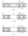
- FIG. 1A an object 101 to be processed having wiring layers 34 and 35 and insulating layers 32 and 33 disposed in this order on both sides of a base layer 31 and metal layers 51 and 52 disposed on the surfaces of the insulating layers 32 and 33 is prepared.
- Fig. 1A and below-mentioned figures are partial cross-sectional views.
- through-holes 41 have been previously bored in predetermined locations, interlayer connecting layers 42 have been disposed on the inner peripheral side surfaces of the through-holes 41, and resin filler 43 is disposed in spaces surrounded by the interlayer insulating layers 42.
- the through-holes 41 also penetrate metal layers 51 and 52, and the interlayer connecting layers 42 are in contact and electrically connected with the metal layers 51 and 52 exposed in the through-holes 41 at the upper and lower ends of the through-holes 41. Therefore, as described later, when the metal layers 51 and 52 are patterned to form wiring layers 36 and 37, the interlayer connecting layers 42 and the wiring layers 36 and 37 which are in contact therewith, are electrically connected with each other.
- the through-holes 41 also penetrate the wiring layers 34 and 35 on the base layer 31, and as similar to the case of the metal layers 51 and 52, the interlayer connecting layers 42 are in contact and electrically connected with the wiring layers 34 and 35 exposed to the inner peripheral surfaces of the through-holes 41. As a result, the wiring layers 34 to 37 in different layers are electrically connected with one another through the interlayer connecting layers 42.
- a large-diameter hole 11 penetrating the object 101 to be processed in the thickness direction thereof is formed.
- both ends of the hole 11 are opened.
- a supporting film 55 is adhered on one side of a substrate 102 to be processed, one end of the hole 11 is closed with the supporting film 55, and a substrate 103 to be processed having a vessel-like space opened at the other end is obtained.
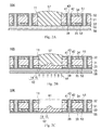
- first photoreactive material made of liquid photo-curing material which becomes the material of micro convex lenses 15 has been prepared.
- the object 103 to be processed is disposed in such a manner that the supporting film 55 faces vertically downward and the open end of the hole 11 faces vertically upward, and liquid first photoreactive material is injected into the hole 11.
- organic material is used herein, but inorganic material, photo-curing material, or photodissolution material may be used.
- organic material is used, but inorganic material may be used.
- the reference numeral 104 in Fig. 2A denotes an object to be processed in the above state. Since the bottom face of the hole 11 is closed with the supporting film 55 which is fluid-tight, the first photoreactive material 57 does not leak from the inside of the hole 11.
- a mask 58 is disposed under the object 104 to be processed and near the supporting film 55, and exposure light 44 is irradiated to the mask 58 as shown in Fig. 2B .
- the mask 58 Since the mask 58 has light-shielding portions described later so as to partially pass the exposure light 44, and the supporting film 55 is transparent to the exposure light 44, the exposure light 44 which has passed through the mask 58 and the supporting film 55 enters the first photoreactive material 57.
- the first photoreactive material 57 is resin cured when irradiated with the exposure light 44.
- the exposure light 44 having an irradiation shape corresponding to the pattern of the mask 58 is irradiated, so that the first photoreactive material 57 is cured to form an optical condensing portion 12 constituted by the cured portion corresponding to the pattern of the mask 58.
- the reference numeral 105 in Fig. 2B denotes an object to be processed in the state that the optical condensing portion 12 has been formed.
- the exposure light is ultraviolet light, visible light, electron beams or the like and widely includes electromagnetic wave and particle beams which cure the first photoreactive material (or below-mentioned second photoreactive material) to form a shape corresponding to the pattern of a mask.
- the mask 58 used in this embodiment is a pattern as shown in Fig. 12A and has light-shielding portions 151 shielding the exposure light 44 arranged in a predetermined pattern on a glass substrate. There are light-passing portions 152 where the exposure light 44 passes through, between the light-shielding portions 151.
- the mask 58 has a plurality of lens patterns 153 having the circular light-shielding portions 151 and the circular light-passing portions 152 arranged alternately and concentrically, and a light attenuation pattern 154 which is arranged around each of the lens patterns and has linear light-shielding portions 151 and linear light-passing portions 152 arranged alternately.
- the area ratio of the light-passing portions 152 to the light-shielding portions 151 in the light attenuation pattern 154 of the mask 58 is set to be less than the area ratio of the light-passing portions 152 to the light-shielding portions 151 in the lens patterns 153 of the mask 58, so that the amount of exposure light 44 which has passed through the light attenuation pattern 154 is less than the amount of exposure light 44 which is passed through the lens patterns 153.
- the widths of the light-passing portions 152 are set to be larger nearer to the centers of concentric circles, and the widths of the light-shielding portions are set to be larger nearer to the outermost periphery of the concentric circles.
- the area ratio of the light-passing portions 152 to the light-shielding portions 151 in the lens patterns 153 becomes larger nearer to the centers of the concentric circles and smaller nearer to the outermost peripheries of the concentric circles.
- the amount of exposure light 44 which has passed through the mask 58 is small at the light-passing portions of the light attenuation pattern 154 and increases nearer to the center of each of the lens patterns 153, so that the amount of exposure light 44 which has passed through locations near the centers of the lens patterns 153 is larger than that of exposure light 44 which has passed through the light attenuation pattern 154, and the exposure light 44 which has passed through locations near the centers of the lens patterns 153 reaches deep portions of the first photoreactive material 57.
- portions to which the exposure light 44 passed through the lens patterns 153 is irradiated are cured in the form of a convex lens which is thick in the middle, and these portions form micro convex lenses 15.
- the same amount of exposure light 44 which has passed through the light attenuation pattern 154 reaches portions around the micro convex lenses 15 and the portions are cured evenly.
- a supporting portion 14 shaped like a board having a constant thickness which is thinner than the micro convex lenses 15 is formed, and the micro convex lenses 15 and the supporting portion 14 constitute the optical condensing portion 12.
- the supporting portion 14 is in contact and fixed with the inner peripheral surface of the hole 11, and the micro convex lenses 15 are fixed in the hole 11 by the supporting portion 14. In the state of Fig. 2B , the micro convex lenses 15 are also fixed on the supporting film 55.
- a substrate 106 to be processed having a cavity 61 formed on the optical condensing portion 12 in the hole 11 is obtained as shown in Fig. 2C .
- liquid first filling material 62 is injected into the cavity 61.
- the first filling material 62 does not leak even if the supporting film 55 has been removed.
- the supporting film 55 is not removed to be remained and the bottom face of the hole 11 is closed by the supporting film 55.
- an object 107 to be processed having the cavity 61 filled with the first filling material 62 is formed.
- the first fillingmaterial 62 is disposed in the hole to the extent that it protrudes from the surface of the object 107 to be processed.
- the first filling material 62 may have any curability including thermosetting property and photo-curability, but the cured material 63 needs to be transparent to an optical signal.
- the bottom face of the curedmaterial 63 is in close contact with the optical condensing portion 12, and the top of it protrudes upward from the surface of the object 108 to be processed.
- the filling portion 13 and the optical condensing portion 12 are in close contact with each other, and constitute a lens section 10. Since the bottom faces of the micro convex lenses 15 and the bottom face of the supporting portion 14 are flat, an optical signal almost vertically irradiated to the lens section 10 enters the inside thereof vertically.
- the irradiated optical signal enters the inside of the lens section 10 without being scattered and is output to the outside of the lens section 10 without being dispersed.
- the refractive index of material consisting of the filling portion 13 is less than that of material consisting of the micro convex lenses 15 (cured first photoreactive material), and an optical signal passing through any one of the micro convex lenses 15 is condensed by the micro convex lens 15, as described above.
- the refractive index of the micro convex lens 15 be 1.05 or more times larger than the refractive index of the filling portion 13.
- the micro convex lens 15 may be made of epoxy resin having the refractive index of 1.584
- the filling portion 13 may be made of epoxy resin having the refractive index of 1.448.
- Resin consisting of the micro convex lenses 15 and resin consisting of the filling portion 13 need to be transparent to an optical signal and have refractive indexes satisfying the above relation, and may be various resin such as silicon resin and acrylic resin in addition to epoxy resin.
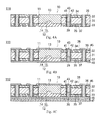
- the supporting film 55 may be removed before or after polishing the filling material 63. After removing the supporting film 55, the metal films 51 and 52 are patterned to obtain an object 110 to be processed having wiring layers 36 and 37 on the insulating layers 32 and 33 as shown in Fig. 4A .
- resin layers are formed on the object 110 to be processed and patterned to obtain an object 111 to be processed having protection layers (solder resist films) 45 and 46 which are the resin layers as shown in Fig. 4B .
- openings 38 are formed at predetermined locations, and the surface of the outermost wiring layer 36 or 37 is exposed to the bottom face of the openings 38.
- the outermost wiring layer 36 or 37 is covered at portions other than the opening 38.
- optical waveguides are adhered on one side of the object 111 to be processed.
- optical waveguides 47 in three layers are attached on a side on which the optical condensing portion 12 is located.
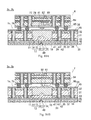
- the object 112 to be processed is cut by a dicing device or the like to form notch 50, which have surface 54 inclined about 45 degrees to the optical waveguides 47, in portions of the optical waveguides 47 on the extension lines of the optical axes 56 of the micro convex lenses 15.
- the reference numeral 49 in this figure denotes a reflector constituted by a notch 50, the inclined surface 54 thereof, and a reflecting layer 53.
- An optical signal input from a micro convex lens 15 to a reflector 49 or an optical signal input from an optical waveguide 47 to a reflector 49 is reflected not by the surface but by the bottom face of the reflecting layer 53, and the traveling direction of the optical signal is changed about 90 degrees.
- the micro convex lenses 15 are fixed in the hole 11 by the supporting portion 14.
- the optical and electrical circuit board 1a of the present invention does not necessarily need to have the supporting portion 4.
- the first photoreactive material 57 is exposed to light through a mask having a pattern by which the supporting portion 14 is not formed and is different from the above-described mask 58.
- the mask 59 in Fig. 12B has the same lens patterns 153, and a light-shielding pattern 155 constituted by light-shielding potions 151 is disposed outside the lens patterns 153.
- exposure light 44 does not pass through the outside of the lens patterns 153.
- micro convex lenses 15 are fixed on the a supporting film 46, but the hole 11 around the micro convex lenses 15 is filled with uncured first photoreactive material 13, so that the micro convex lenses 15 are not fixed to the inner peripheral surface of the hole 11.
- first filling material When first filling material is injected into the hole 11 of the object 126 to be processed to the extent that the surface of the first filling material protrudes and then, the first filling material is cured.
- An object 127 to be processed having cured first filling material 63 formed in the hole 11 is obtained as shown in Fig. 6C .
- an object 128 to be processed is obtained.
- the metal layers 51 and 52 of the object 128 to be processed are patterned, an object 129 to be processed having patterned wiring layers 36 and 37 as outermost layers is obtained.
- the isolated micro convex lenses 15 are fixed to the inner peripheral surface of the hole 11 by the cured material 63, so that the micro convex lenses 15 do not drop out of the hole 11 even if the supporting film 46 has been removed.
- optical and electrical circuit board 1d of this variation can be used instead of the optical and electrical circuit board 1a of the first embodiment (or the optical and electrical circuit board 1b of the second embodiment or the optical and electrical circuit board 1c of the third embodiment described later) to mount the optical-electrical signals conversion substrate 6, 7 in order to obtain an optical and electrical circuit board having the optical-electrical signals conversion substrate 6, 7.
- the micro convex lenses 15 are formed first and the filling portion 13 is formed next.
- the method of the present invention is not limited to this.
- micro convex lenses 15 are disposed in the same locations as those of the first optical and electrical circuit board 1a of the first embodiment and the optical and electrical circuit board 1d of the variation, an object 102 to be processed having a hole 11 penetrating it in the thickness direction as shown in Fig. 1B is formed. Then, as shown in Fig. 8A , a supporting film is attached on a side opposite to a side on which a supporting film is attached when the optical and electrical circuit board 1a of the first embodiment or the optical and electrical circuit board 1d of the variation is formed.
- the reference numeral 133 in Fig. 8A denotes an object to be processed in this state, and one end of the hole 11 is closed by a supporting film 66.
- the object 133 to be processed is placed in such a manner that the supporting film 66 faces vertically downward and the opening end of the hole 11 faces vertically upward, and as shown in Fig. 8B , liquid second photoreactive material 67 is injected into the hole 11.
- photo-curing material is used for the second photoreactive material.
- an object 134 to be processed is illustrated as upper part of the sheet shows vertical lower side and bottom part of the sheet shows vertical upper side, as in contrast to an object to be processed in Fig. 2A or Fig. 3A .
- a mask 68 is disposed, as shown in Fig. 8C , exposure light is irradiated to the mask 68.
- the supporting film 66 is transmissive to exposure light 44.
- the exposure light 44 which has passed through the mask 68 and the supporting film 66 is irradiated to the photoreactive material 67 to form a filling portion 13 cured in a form corresponding to the pattern of the mask 68.
- the mask 68 has a plurality of concave lens patterns each having optical transmittance which is low in the middle and higher nearer to the outermost periphery, arranged in a light attenuation pattern.
- a concave part 65 is formed in the filling portion 13.
- the filling portion has transparency to the optical signal.
- the reference numeral 135 shown in Fig. 8C denotes an object to be processed in the state that the filling portion 13 having concave parts 65 is formed, and uncured second photoreactive material 67 is remained on the filling portion 13.
- the object 136 to be processed is placed in such a manner that the cavity 69 faces vertically upward and the filling portion 13 side faces vertically downward, and liquid second filling material is injected into the cavity 69 and is cured.
- the second filling material may have any curability including thermosetting property and photo-curability like the first filling material 62.
- an object 137 to be processed having cured material 70 having the surface of which has protruded is obtained as shown in Fig. 9B .
- the cured material 70 is transparent to an optical signal.
- the protruded portion of the cured material 70 is grinded to be flattened by a grinder or the like to form an optical condensing portion 12 made of the cured second filling material 70.
- Portions of the optical condensing portion 12 filled in the concave parts 65 of the filling portion 13 are each shaped like a convex lens to form micro convex lenses 15.
- a flat plane is formed around the concave parts 65 of the filling portion 13, and a portion of the optical condensing portion 12 located on the flat plane shapes a flat plate to form a supporting portion 14.
- the optical condensing portion 12 is in close contact with the filling portion 13, and the micro convex lenses 15 are fixed inside the hole 11 by the filling portion 13 and the supporting portion 14.
- the refractive index of the cured material 70 of the second fillingmaterial consisting of the micro convex lenses is larger than that of the cured material of the second photoreactive material consisting of the filling portion 13, so that light passing through the micro convex lenses 15 and the filling portion 13 is condensed at the boundaries between the micro convex lenses 15 and the filling portion 13.
- a convex lens section 10 having a filling portion 13 made of the second photoreactive material and an optical condensing portion 12 made of the second filling material obtained by the above process has the same structure as that of a convex lens section 10 having an optical condensing portion made of the first photoreactive material 57 and a filling portion made of the first filling material 62, and after a convex lens section 10 has been formed, the optical and electrical circuit board 1b ( Fig. 5B ) of the second embodiment of the present invention is obtained by the same processing as shown in Fig. 4A to Fig. 5A for the objects 109 to 113 to be processed of the first embodiment.
- an optical-electrical signals conversion substrate 6, 7 is mounted on the optical and electrical circuit board 1b of the second embodiment as in the case of the optical and electrical circuit board 1a of the first embodiment to obtain an optical and electrical circuit board 2b, 3b.
- the optical condensing portion 12 is made of photo-curing material.
- the optical condensing portion 12 may be made of thermosetting resin, photo-curing material, or any other curing resin.
- the optical condensing portion 12 is disposed between the filling portion 13 and the optical waveguides 47.
- the present invention is not limited thereto, and the filling portion 13 may be disposed between the optical condensing portion 12 and the optical waveguides 47 by disposing the supporting film 55, 66 on the other side.
- the reference numeral 1c in Figs. 11A and 11B denotes the optical and electrical circuit board of the third embodiment of the present invention having such a structure
- the reference numerals 2c, 3c denotes the optical and electrical circuit board on which the optical-electrical signals conversion substrate 6, 7 is mounted.
- optical and electrical circuit boards 1c to 3c have the same structures as those of the optical and electrical circuit boards 1a to 3a of the first embodiment or the optical and electrical circuit boards 1b to 3b of the second embodiment except that position of the optical condensing portion 12 and the filling portion 13 change in the hole 11.
- an optical signal which has traveled in an optical waveguide 47 and has been reflected by a reflector 49 firstly passes through the filling portion 13 and is then condensed by a micro convex lens 15 to enter the optical-electrical signals conversion substrate 6, 7.
- an optical signal output from the optical-electrical signals conversion substrate 6, 7 is condensed by a micro convex lens 15, passes through the filling portion 13, enters a reflector 49, and is guided inside the optical waveguide 47.
- the micro convex lenses 15 may be fixed in the hole 11 by the filling portion 13 without providing a supporting portion 14 as in the case of the optical and electrical circuit board 1d of the variation.
- optical and electrical circuit boards 1c to 3c of the third embodiment as in the case of the optical and electrical circuit boards 1a to 3a of the first embodiment of the present invention or the optical and electrical circuit boards 1b to 3b of the second embodiment of the present invention.
- the portion of the holes 11 other than the optical condensing portion 12 can be filled with air without providing the filling portion 13 as long as the micro convex lenses 15 are fixed to the inner peripheral side surface of the hole 11 by the supporting portion 14.
- the thickness of the supporting portion 14 and the thicknesses of the micro convex lenses 15 can be changed by changing the amount of exposure light 44 and/or the ratio between the light-shielding portions 151 and the light-passing portions 152 of the mask 58 and 59.
- the distances between the micro convex lenses 15 and the light-emitting/receiving elements 82, 92 can be also changed.
- the distances between the micro convex lenses 15 and the light-emitting/receiving elements 82, 92 can also be changed by changing the thickness of the multi-layer substrate section 30.
- first and second photoreactive material and the first and second filling material are liquid, they are not necessarily limited to liquid, and may be paste material or powder material as long as they can be disposed at a predetermined location in the hole 11.
- the optical condensing portion 12 is made of first photoreactive material in one exposure step, but may be formed in two or more steps.
- first photoreactive material is exposed to light through a mask having no lens section to form a supporting portion 14 having no micro convex lens as shown in Fig. 13A , and the soluble portion thereof is then removed. After that, first photoreactive material is filled again and exposed to light to form micro convex lenses 15 on the supporting portion 14 as shown in Fig. 13B .
- the first or second photoreactive material is photo-curing material.
- the optical condensing portion 12 may be formed by using photodissolution material.
- photodissolution material portions to which exposure light is irradiated become soluble portion and portions to which exposure light is not irradiated become cured portion, so that when forming a component having the same shape as that in the case that photo-curing material is used, the pattern of a mask is reversed from that in the case that photo-curing material is used.
- an optical condensing portion and a filling portion can be formed in the same process as that in the case of photo-curing material.
- photo-curing material has more handling and cost advantages than photodissolution material.
Landscapes
- Physics & Mathematics (AREA)
- General Physics & Mathematics (AREA)
- Optics & Photonics (AREA)
- Engineering & Computer Science (AREA)
- Microelectronics & Electronic Packaging (AREA)
- Optical Integrated Circuits (AREA)
- Optical Couplings Of Light Guides (AREA)
- Structure Of Printed Boards (AREA)
Abstract

Description
- The present invention relates to an optical and electrical circuit board, and in particular to an optical and electrical circuit board having a micro convex lens and a method of manufacturing the same.
- In recent years, the amount of communication data of the Internet or the like is increasing dramatically, and a technology for realizing high speed and large capacity communication using an optical signal by converting an electrical signal in a signal processor and an optical signal transmitted through an optical fiber to each other become increasingly important.
- An optical and electrical circuit board having a structure that a microlens condensing an optical signal is disposed between an optical signal receiving/transmitting element and an optical waveguide in order to convert an electrical signal and an optical signal to each other, has been proposed.
- Methods of forming such a microlens include a method using a mold, a forming method by dropping lens material, a method of forming a lens by heating and softening lens material cylindrical shaped, a method of exposing lens material to exposure light which has passed through a mask. In each of the conventional manufacturing methods, a mirolens is formed separately from an optical and electrical circuit board and is mounted on the optical and electrical circuit board, so that the cost of mounting the microlens is high and alignment of the microlens to the substrate is difficult.
- A method of forming a microlens using a mask is described in, for example, the following document 1.
- Patent Document 1: Japanese Patent Application Laid-open No.
8-286002 - The present invention has been developed to solve the problems of the above-described prior art, and the first object of the present invention is to provide a technology of forming a microlens directly on a substrate.
- Furthermore, the second object of the present invention is to provide a technology capable of allowing a microlens to be incorporated in a substrate.
- In order to solve the above problems, the present invention is an optical and electrical circuit board including a patterned electrical wiring and a micro convex lens provided in at least one hole formed in the optical and electrical circuit board.
- Furthermore, the present invention is an optical and electrical circuit board including, in the hole, a connecting portion is formed in order to connect and fix the micro convex lens to an inner peripheral side surface of the hole.
- Furthermore, the present invention is an optical and electrical circuit board, including an optically transparent filling portion being disposed in the hole, and a refractive index of the filling portion is smaller than a refractive index of the micro convex lens.
- Furthermore, the present invention is an optical and electrical circuit board including a wiring substrate having an insulating substrate and the electrical wiring, and the hole penetrates the wiring substrate in a thickness direction of the wiring substrate.
- Furthermore, the present invention is an optical and electrical circuit board including an optical waveguide which is a transmission path of an optical signal passing through the micro convex lens.
- Furthermore, the present invention is a method of manufacturing an optical and electrical circuit board including filling first photoreactive material into at least one hole which is formed in a substrate having a patterned electrical wiring and which pass through the substrate in a thickness direction thereof, partially exposing the first photoreactive material from one opening side of the hole to form a cured portion and a soluble portion, and then dissolving and removing the soluble portion of the first photoreactive material to form a micro convex lens in the hole.
- Furthermore, the present invention is a method of manufacturing an optical and electrical circuit board further including providing an optically transparent supporting film on one side of the substrate to close said one opening of the hole, injecting the first photoreactive material into the hole from another opening of the hole after providing the optically transparent supporting film, and exposing the first photoreactive material through the supporting film and developing the firs photoreactive matirial.
- Furthermore, the present invention is a method of manufacturing an optical and electrical circuit board including, forming a cured portion in a region between a portion in which the micro convex lens is formed and an inner peripheral side surface of the hole, and the cured portion constitutes a connecting portion which connects the micro convex lens to the inner peripheral side surface of the hole.
- Furthermore, the present invention is a method of manufacturing an optical and electrical circuit board including, filling first filling material having optical transparency and a refractive index smaller than a refractive index of the micro convex lens into the hole in which the micro convex lens has been formed; and curing the first filling material to form a filling portion.
- Furthermore, the present invention is a method of manufacturing an optical and electrical circuit board including, filling second photoreactive material into a hole which is formed in a substrate having a patterned electrical wiring and which passes through the substrate in a thickness direction thereof; partially exposing the second photoreactive material from one opening side of the hole to form a cured portion and a soluble portion, then dissolving and removing the soluble portion of the second photoreactive material to form a filling portion having a concave part in the hole, filling second fillingmaterial having optical transparency and a refractive index higher than a refractive index of the filling portion in the concave part, and then curing the second filling material to form a micro convex lens.
- Furthermore, the present invention is a method of manufacturing an optical and electrical circuit board, including, providing an optically transparent supporting film on one side of the substrate to close said one opening of the hole, injecting the second photoreactive material into the hole from another opening of the hole after providing the optically transparent supporting film, and exposing the second photoreactive material through the supporting film.
- Furthermore, the present invention is a method of manufacturing an optical and electrical circuit board, including for the exposing, using a mask having a plurality of lens patterns in which circular light-shielding portions having circle shape and circular light-passing portions having circle shape are arranged alternately and concentrically, and a light attenuation pattern which is located around each of the lens patterns and has linear light-shielding portions having line shape and linear light-passing portions having line shape arranged alternately.
- Furthermore, the present invention is a method of manufacturing an optical and electrical circuit board, wherein the mask is configured such that an area ratio of an area of the linear light-passing portions to an area of the linear light-shielding portions in the light attenuation pattern is set to be less than an area ratio of an area of the circular light-passing portions to an area of the circular light-shielding portions in the lens patterns.
- Furthermore, the present invention is a method of manufacturing an optical and electrical circuit board, wherein the mask is configured such that, in the lens patterns, widths of the circular light-passing portions are set to be larger nearer to a center of concentric circles, and widths of the circular light-shielding portions are set to be larger nearer to an outermost periphery of the concentric circles.
- Furthermore, the present invention is a method of manufacturing an optical and electrical circuit board, including, when forming the micro convex lens, exposing a portion in a region between a portion in which the depression is formed and an inner peripheral side surface of the hole in order to form a connecting portion which connects the micro convex lens to the inner peripheral side surface of the hole.
- The present invention is configured as described above, and when the photoreactive material is photo-curing material, a portion where exposure light has been irradiated is cured to become a cured portion, and a portion to which exposure light is not irradiated becomes a soluble portion. When the photoreactive material is photodissolution material, it is temporarily cured and then exposed using a mask. The portion to which exposure light has been irradiated becomes a soluble portion and a portion to which exposure light is not irradiated becomes a cured portion.
- In the present invention, exposure light which has passed through a mask is irradiated to photoreactive material disposed in a hole of an object to be processed to form a cured portion and a soluble portion, and a micro convex lens is made of the photoreactive material, or, a filling portion having a depression part is made of photoreactive resin by exposure light which has passed through the mask and liquid filling material such as thermosetting resin is disposed in the depression part and is cured to form a micro lens.
- It is easy to align an object to be processed with a mask, so that a micro convex lens can be disposed in an accurate position as compared with the case that a micro convex lens formed separately from the object to be processed is mounted.
- Furthermore, a micro convex lens can be formed by an exposing and developing process similar to that of patterning a wiring layer, a protection layer, and the like in an object to be processed, so that the workability is high.
- Furthermore, a micro convex lens is incorporated in an optical and electrical circuit board, so that the optical and electrical circuit board can be handled easily.
-
-
Figs. 1A to 1C illustrate a process of manufacturing the optical and electrical circuit board of a first embodiment of the present invention:Fig. 1A shows a step of forming metal layers,Fig. 1B shows a step of forming a hole, andFig. 1C shows a step of adhering a supporting film. -
Figs. 2A to 2C illustrate the process of manufacturing the optical and electrical circuit board of the first embodiment of the present invention:Fig. 2A shows a step of filling first photoreactive material,Fig. 2B shows a step of forming micro convex lenses supported by a supporting portion, andFig. 2C shows a step of removing uncured first photoreactive material. -
Figs. 3A to 3C illustrate the process of manufacturing the optical and electrical circuit board of the first embodiment of the present invention:Fig. 3A shows a step of filling first filling material,Fig. 3B shows a step of curing, andFig. 3C shows a step of grinding. -
Figs. 4A to 4C illustrate the process of manufacturing the optical and electrical circuit board of the first embodiment of the present invention:Fig. 4A shows a step of patterning metal layers,Fig. 4B shows a step of forming a protection layer, andFig. 4C shows a step of forming optical waveguides. -
Figs. 5A and 5B illustrate the process of manufacturing the optical and electrical circuit board of the first embodiment of the present invention:Fig. 5A shows a step of forming notches, andFig. 5B shows a step of forming reflectors. -
Figs. 6A and 6B illustrate a process of manufacturing the optical and electrical circuit board of a variation of the present invention:Fig. 6A shows a step of forming isolated micro convex lenses,Fig. 6B shows a step of removing remained first photoreactive material, andFig. 6C shows a step of filling first filling material. -
Figs. 7A to 7C illustrate the process of manufacturing the optical and electrical circuit board of the variation of the present invention:Fig. 7A shows a step of removing a supporting film,Fig. 7B shows a step of patterning metal layers, andFig. 7C shows a step of forming optical waveguides and reflectors. -
Figs. 8A to 8C illustrate a process of manufacturing the optical and electrical circuit board of a second embodiment of the present invention:Fig. 8A shows a step of adhering a supporting film to a side opposite to a side in the case of the first embodiment,Fig. 8B shows a step of filling second photoreactive material, andFig. 8C shows a step of forming a filling portion having a depression. -
Figs. 9A to 9C illustrate a process of manufacturing the optical and electrical circuit board of the second embodiment of the present invention:Fig. 9A shows a step of removing uncured second photoreactive material,Fig. 9B shows a step of injecting and curing second filling material, andFig. 9C shows a step of grinding. -
Fig. 10A illustrates the state that an example of an optical-electrical signals conversion substrate is mounted on the optical and electrical circuit board of the first embodiment or the second embodiment, andFig. 10B illustrates the state that another example of an optical-electrical signals conversion substrate is mounted on the optical and electrical circuit board of the first embodiment or the second embodiment. -
Fig. 11A illustrates the state that an example of an optical-electrical signals conversion substrate is mounted on the optical and electrical circuit board of the third embodiment, andFig. 11B illustrates the state that another example of an optical-electrical signals conversion substrate is mounted on the optical and electrical circuit board of the first and second embodiments. -
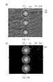
Fig. 12A shows an example of a mask for forming micro convex lenses, andFig. 12B shows another example of a mask for forming micro convex lenses; and -
Figs. 13A and 13B illustrate an example of forming a supporting portion and micro convex lenses by two or more exposure processes. -
- 1a to 1d, 2a to 2c, and 3a to 3c: Optical and electrical circuit board,
- 11: Hole
- 13: Filling portion
- 14: Connecting portion
- 15: Micro convex lense
- 34 to 37: Wiring layers
- 46, 66: Supporting film
- 65: concave part
- The
reference numeral 1a inFig. 5B denotes a first embodiment of an optical and electrical circuit board of the present invention. - An optical and
electrical circuit board 1a has amulti-layer substrate section 30 and alens section 10. Themulti-layer substrate section 30 is structured in such a manner that one or more layers of substrate, insulating layers, and wiring layers which are electrical wirings are laminated. Themulti-layer substrate section 30 has abase layer 31, patterned wiring layers 34 and 35 are disposed on the top surface and back surface of thebase layer 31, insulatinglayers base layer 31, and patterned wiring layers 36 and 37 are disposed on the surfaces of the insulatinglayers base layer 31 and the insulatinglayers - In this embodiment, only one of the insulating
layers base layer 31, and only two of the wiring layers 34 to 37 including wiring layers 36 and 37 on the insulatinglayers base layer 31. However, a multi-layer substrate having three or more layers on one side including insulating layers and wiring layer further laminated is also included in themulti-layer substrate section 30 of the present invention. - In addition, on the surfaces of the outermost wiring layers 36 and 37, protection layers 45, 46 (also known as solder resist layers) are disposed so as to cover the wiring layers 36 and 37, respectively, in order that the optical and
electrical circuit board 1a is not shorted to external electric components. - For the
base layer 31 and the insulatinglayers - In the
multi-layer substrate section 30, through-holes 41 penetrating it in the thickness direction thereof are formed, and conductiveinterlayer connecting layer 42 composed of electroless plating layer is formed on the inner peripheral surface of the through-hole 41. The inside of the through-hole 41, that is, space surrounded by theinterlayer connecting layer 42, is filled withresin filler 43. - The
interlayer connecting layer 42 is in contact with part of wiring layers 34 to 37 and mutually connect the wiring layers 34 to 37 located in different layers so that electrical signal is transmitted between the wiring layers 34 and 37 in different layers through the interfacial connecting layers 42. - Next, a
hole 11 having a diameter larger than that of the through-hole 41 is formed in themulti-layer substrate section 30, and thelens section 10 is disposed in thehole 11. - The
lens section 10 has anoptical condensing portion 12 for condensing light and a fillingportion 13 which fills a portion other than the optical condensingportion 12 inside thehole 11. - The
optical condensing portion 12 is disposed at an end of thehole 11, and the fillingportion 13 is located on the opposite side of the optical condensingportion 12 in thehole 11. - The
optical condensing portion 12 has one or more microconvex lenses 15 and a supportingportion 14 located on side faces of the microconvex lenses 15. - The micro
convex lenses 15 are located apart from the inner peripheral side surface of thehole 11, and the supportingportion 14 is in contact with the inner peripheral side surface of thehole 11 and is fixed to the contact portion, so that each of the microconvex lenses 15 is fixed to the inner peripheral side surface of thehole 11 through the supportingportion 14. - Furthermore, the optical condensing
portion 12 and the fillingportion 13 are in close contact with each other, and the filling portion is in contact with the inner peripheral side surface of thehole 11 and is fixed to the contact portion. The microconvex lenses 15 are in close contact with the fillingportion 13 and are fixed to the close contact portion, so that the microconvex lenses 15 are also fixed to the inner peripheral side surface of thehole 11 through the fillingportion 13. - On a surface of the
multi-layer substrate section 30, anoptical wave guide 47 is extended for each of the microconvex lenses 15 in such a manner that theoptical waveguides 47 cross the intersection position ofoptical axis 56 of the microconvex lens 15. - In positions where the
optical waveguides 47 intersect theoptical axes 56 of the microconvex lenses 15, areflector 49 is provided for each of theoptical waveguides 47. - The
optical waveguides 47 are located in the planes which are parallel to each other including the same plane. When an optical signal is transmitted in each ofoptical waveguide 47 and enters areflector 49, the optical signal is reflected from a direction substantially perpendicular to the plane where theoptical waveguide 47 is located. In contrast, when an optical signal enters areflector 49 in a direction substantially perpendicular to a plane where theoptical waveguide 47 is located, the optical signal is reflected in a direction substantially perpendicular in order to guide the optical signal to the inside of theoptical waveguide 47. - The refractive index of a constituent material of the optical condensing
portion 12, particularly the microconvex lenses 15 is larger than that of a constituent material of the fillingportion 13, and the microconvex lenses 15 have a shape near a hemisphere which is thick in the middle and thinner nearer the outer periphery than the middle. Portion swelling thick is in close contact with the filling portion. Thus, both of an optical signal entering the fillingportion 13 through the microconvex lens 15 and an optical signal entering the microconvex lens 15 through the fillingportion 13 are condensed. - The micro
convex lens 15 is located in the traveling direction of an optical signal reflected in a direction substantially perpendicular to a plane where theoptical waveguide 47 is located, and the reflected optical signal enters the microconvex lens 15 in parallel with theoptical axis 56, is condensed, and is released to the outside of themulti-layer substrate section 30 through the fillingportion 13. - In contrast, an optical signal passes through the filling
portion 13 and enters a microconvex lens 15 in parallel with theoptical axis 56. In the traveling direction of the optical signal condensed by the microconvex lens 15, thereflector 49 is located. When the condensed optical signal enters thereflector 49 in a direction substantially perpendicular to a plane where theoptical waveguide 47 is located, it is reflected almost vertically and guided into theoptical waveguide 47. - On the optical and
electrical circuit board 1a of the present invention (and below-mentioned optical andelectrical circuit boards 1b to Id), various electrical or optical components and substrates can be mounted. - The
reference numerals Figs. 10A and 10B denote an optical and electrical circuit board on which an optical-electricalsignals conversion substrate - The optical-electrical
signals conversion substrate elements signals conversion substrate elements elements - First, in
Fig. 10A , the optical-electricalsignals conversion substrate 6 has arecess 77 inside thereof, and the light-emitting/receivingelements 82 are disposed in therecess 77. - The optical-electrical
signals conversion substrate 6 is disposed in such a manner that the light-receivingelements 82 are located on the extension lines of theoptical axes 56 of the microconvex lenses 15. - The optical-electrical
signals conversion substrate 6 hasconvex lenses 81, which are disposed just above the light-emitting/receivingelements 82. Inside of therecess 77 is filled with fillingmaterial 78 transparent to an optical signal. - When a light-emitting/receiving
element 82 operates as a light-receiving element, an optical signal which has been transmitted in anoptical waveguide 47 in the optical andelectrical circuit board 1a and reflected by thereflector 49 is condensed by anoptical condensing portion 12 and aconvex lens 81, enters the light-emitting/receivingelement 82, and then is converted to an electrical signal. - When a light-emitting/receiving
element 82 operates as a light-emitting element, an electrical signal input from thewiring layer 84 is converted to an optical signal and transmitted by the light-emitting/receivingelement 82. The optical signal output from the light-emitting/receivingelement 82 is condensed by aconvex lens 81 and the optical condensingportion 12 and reflected by thereflector 49 to be guided into theoptical waveguide 47. - A micro
convex lens 15 is disposed for each of the light-emitting/receivingelements 82, and an optical signal transmitted from each of the light-emitting/receivingelements 82 is condensed by the microconvex lens 15. - The optical-electrical
signals conversion substrate 7 inFig. 10B has nodepression 77 orconvex lens 81, and light-emitting/receivingelements 92 anddriver ICs 93 are exposed on a surface thereof. However, operations of transmitting and receiving an optical signal are equivalent to those in the case ofFig. 10A . - The
wiring layer 36 of the optical andelectrical circuit board 1a is electrically connected with the wiring layers 84, 94 of the optical-electricalsignals conversion substrate 67 throughconductive bumps signals conversion substrate electrical circuit board 1a, an optical signal is transmitted unidirectionally or bi-directionally through thelens section 10, but an electrical signal is transmitted unidirectinally or bi-directinally through thebumps - Protection layers 45 and 46 are disposed on the surface of the optical and
electrical circuit board 1a and between thelens section 10 and theoptical waveguides 47, and the protection layers 45, 46 are transparent to an optical signal, thus not interfering with transmission of an optical signal. - Furthermore, electronic components such as semiconductor elements and capacitors may also be mounted on the optical and
electrical circuit board 1a in order to constitute electronic circuits. - The process of manufacturing an optical and
electrical circuit board 1a as described above will be described. - First, as shown in
Fig. 1A , anobject 101 to be processed havingwiring layers layers base layer 31 andmetal layers layers Fig. 1A and below-mentioned figures are partial cross-sectional views. - In the
object 101 to be processed ofFig. 1A , through-holes 41 have been previously bored in predetermined locations,interlayer connecting layers 42 have been disposed on the inner peripheral side surfaces of the through-holes 41, andresin filler 43 is disposed in spaces surrounded by the interlayer insulating layers 42. - The through-
holes 41 also penetratemetal layers interlayer connecting layers 42 are in contact and electrically connected with the metal layers 51 and 52 exposed in the through-holes 41 at the upper and lower ends of the through-holes 41. Therefore, as described later, when the metal layers 51 and 52 are patterned to form wiring layers 36 and 37, theinterlayer connecting layers 42 and the wiring layers 36 and 37 which are in contact therewith, are electrically connected with each other. - The through-
holes 41 also penetrate the wiring layers 34 and 35 on thebase layer 31, and as similar to the case of the metal layers 51 and 52, theinterlayer connecting layers 42 are in contact and electrically connected with the wiring layers 34 and 35 exposed to the inner peripheral surfaces of the through-holes 41. As a result, the wiring layers 34 to 37 in different layers are electrically connected with one another through the interlayer connecting layers 42. - Next, as shown in
Fig. 1B , a large-diameter hole 11 penetrating theobject 101 to be processed in the thickness direction thereof is formed. - In an
object 102 to be processed in this state, both ends of thehole 11 are opened. Next, as shown inFig. 1C , when a supportingfilm 55 is adhered on one side of asubstrate 102 to be processed, one end of thehole 11 is closed with the supportingfilm 55, and asubstrate 103 to be processed having a vessel-like space opened at the other end is obtained. - In advance, first photoreactive material made of liquid photo-curing material which becomes the material of micro
convex lenses 15 has been prepared. Theobject 103 to be processed is disposed in such a manner that the supportingfilm 55 faces vertically downward and the open end of thehole 11 faces vertically upward, and liquid first photoreactive material is injected into thehole 11. For the first photoreactive material and below-mentioned second photoreactive material, organic material is used herein, but inorganic material, photo-curing material, or photodissolution material may be used. Furthermore, also for the first and second filling material, organic material is used, but inorganic material may be used. - The
reference numeral 104 inFig. 2A denotes an object to be processed in the above state. Since the bottom face of thehole 11 is closed with the supportingfilm 55 which is fluid-tight, the firstphotoreactive material 57 does not leak from the inside of thehole 11. - A
mask 58 is disposed under theobject 104 to be processed and near the supportingfilm 55, andexposure light 44 is irradiated to themask 58 as shown inFig. 2B . - Since the
mask 58 has light-shielding portions described later so as to partially pass theexposure light 44, and the supportingfilm 55 is transparent to theexposure light 44, theexposure light 44 which has passed through themask 58 and the supportingfilm 55 enters the firstphotoreactive material 57. - The first
photoreactive material 57 is resin cured when irradiated with theexposure light 44. Theexposure light 44 having an irradiation shape corresponding to the pattern of themask 58 is irradiated, so that the firstphotoreactive material 57 is cured to form anoptical condensing portion 12 constituted by the cured portion corresponding to the pattern of themask 58. - The
reference numeral 105 inFig. 2B denotes an object to be processed in the state that the optical condensingportion 12 has been formed. - In the present invention, the exposure light is ultraviolet light, visible light, electron beams or the like and widely includes electromagnetic wave and particle beams which cure the first photoreactive material (or below-mentioned second photoreactive material) to form a shape corresponding to the pattern of a mask.
- The
mask 58 used in this embodiment is a pattern as shown inFig. 12A and has light-shieldingportions 151 shielding theexposure light 44 arranged in a predetermined pattern on a glass substrate. There are light-passingportions 152 where the exposure light 44 passes through, between the light-shieldingportions 151. - The
mask 58 has a plurality oflens patterns 153 having the circular light-shieldingportions 151 and the circular light-passingportions 152 arranged alternately and concentrically, and alight attenuation pattern 154 which is arranged around each of the lens patterns and has linear light-shieldingportions 151 and linear light-passingportions 152 arranged alternately. - The area ratio of the light-passing
portions 152 to the light-shieldingportions 151 in thelight attenuation pattern 154 of themask 58 is set to be less than the area ratio of the light-passingportions 152 to the light-shieldingportions 151 in thelens patterns 153 of themask 58, so that the amount of exposure light 44 which has passed through thelight attenuation pattern 154 is less than the amount of exposure light 44 which is passed through thelens patterns 153. - In the
lens patterns 153 of themask 58, the widths of the light-passingportions 152 are set to be larger nearer to the centers of concentric circles, and the widths of the light-shielding portions are set to be larger nearer to the outermost periphery of the concentric circles. Thus, the area ratio of the light-passingportions 152 to the light-shieldingportions 151 in thelens patterns 153 becomes larger nearer to the centers of the concentric circles and smaller nearer to the outermost peripheries of the concentric circles. - According to the area ratio described above, the amount of exposure light 44 which has passed through the
mask 58 is small at the light-passing portions of thelight attenuation pattern 154 and increases nearer to the center of each of thelens patterns 153, so that the amount of exposure light 44 which has passed through locations near the centers of thelens patterns 153 is larger than that of exposure light 44 which has passed through thelight attenuation pattern 154, and theexposure light 44 which has passed through locations near the centers of thelens patterns 153 reaches deep portions of the firstphotoreactive material 57. - As a result, as shown in
Fig. 2B , portions to which theexposure light 44 passed through thelens patterns 153 is irradiated, are cured in the form of a convex lens which is thick in the middle, and these portions form microconvex lenses 15. - The same amount of exposure light 44 which has passed through the
light attenuation pattern 154 reaches portions around the microconvex lenses 15 and the portions are cured evenly. As a result, a supportingportion 14 shaped like a board having a constant thickness which is thinner than the microconvex lenses 15 is formed, and the microconvex lenses 15 and the supportingportion 14 constitute the optical condensingportion 12. - The supporting
portion 14 is in contact and fixed with the inner peripheral surface of thehole 11, and the microconvex lenses 15 are fixed in thehole 11 by the supportingportion 14. In the state ofFig. 2B , the microconvex lenses 15 are also fixed on the supportingfilm 55. - As for an amount of the
exposure light 44 passed through themask 58, even exposure light passed through the centers of thelens patterns 153 is set to have the light amount less than that curing the firstphotoreactive material 57 totally in the depth direction, so that uncured firstphotoreactive material 57 is remained on the optical condensingportion 12. - When the
object 105 to be processed in this state is washed to remove the uncured firstphotoreactive material 57, asubstrate 106 to be processed having acavity 61 formed on the optical condensingportion 12 in thehole 11 is obtained as shown inFig. 2C . - Next, as shown in
Fig. 3A , liquid first fillingmaterial 62 is injected into thecavity 61. - When the
hole 11 has been closed by the optical condensingportion 12, thefirst filling material 62 does not leak even if the supportingfilm 55 has been removed. However, when thehole 11 has not been closed by the optical condensingportion 12, the supportingfilm 55 is not removed to be remained and the bottom face of thehole 11 is closed by the supportingfilm 55. - In either case, as shown in
Fig. 3A , anobject 107 to be processed having thecavity 61 filled with thefirst filling material 62 is formed. Thefirst fillingmaterial 62 is disposed in the hole to the extent that it protrudes from the surface of theobject 107 to be processed. - When the
first filling material 62 is cured in this state, curedmaterial 63 of thefirst filling material 62 is formed on the optical condensingportion 12 in thehole 11. - The
first filling material 62 may have any curability including thermosetting property and photo-curability, but the curedmaterial 63 needs to be transparent to an optical signal. - The bottom face of the
curedmaterial 63 is in close contact with the optical condensingportion 12, and the top of it protrudes upward from the surface of theobject 108 to be processed. - Next, when the surface of the
object 108 to be processed having the curedmaterial 63 is grinded to remove the portion of the curedmaterial 63 protruding from the surface of theobject 108 to be processed, anobject 109 to be processed in which a fillingportion 13 having a plane surface is disposed on the optical condensingportion 12 in thehole 11 is obtained as shown inFig. 3C . - The filling
portion 13 and the optical condensingportion 12 are in close contact with each other, and constitute alens section 10. Since the bottom faces of the microconvex lenses 15 and the bottom face of the supportingportion 14 are flat, an optical signal almost vertically irradiated to thelens section 10 enters the inside thereof vertically. - Furhermore, since the surface of the
lens section 10 is flat, the irradiated optical signal enters the inside of thelens section 10 without being scattered and is output to the outside of thelens section 10 without being dispersed. - The refractive index of material consisting of the filling portion 13 (cured first filling material) is less than that of material consisting of the micro convex lenses 15 (cured first photoreactive material), and an optical signal passing through any one of the micro
convex lenses 15 is condensed by the microconvex lens 15, as described above. - In this embodiment and below-mentioned embodiments, it is desirable that the refractive index of the micro
convex lens 15 be 1.05 or more times larger than the refractive index of the fillingportion 13. As an example, the microconvex lens 15 may be made of epoxy resin having the refractive index of 1.584, and the fillingportion 13 may be made of epoxy resin having the refractive index of 1.448. - Resin consisting of the micro
convex lenses 15 and resin consisting of the fillingportion 13 need to be transparent to an optical signal and have refractive indexes satisfying the above relation, and may be various resin such as silicon resin and acrylic resin in addition to epoxy resin. - The supporting
film 55 may be removed before or after polishing the fillingmaterial 63. After removing the supportingfilm 55, themetal films object 110 to be processed havingwiring layers layers Fig. 4A . - Next, resin layers are formed on the
object 110 to be processed and patterned to obtain anobject 111 to be processed having protection layers (solder resist films) 45 and 46 which are the resin layers as shown inFig. 4B . - In the
protection layer openings 38 are formed at predetermined locations, and the surface of theoutermost wiring layer openings 38. Theoutermost wiring layer opening 38. - Next, optical waveguides are adhered on one side of the
object 111 to be processed. Here, as shown inFig. 4C ,optical waveguides 47 in three layers are attached on a side on which the optical condensingportion 12 is located. Theobject 112 to be processed is cut by a dicing device or the like to formnotch 50, which havesurface 54 inclined about 45 degrees to theoptical waveguides 47, in portions of theoptical waveguides 47 on the extension lines of theoptical axes 56 of the microconvex lenses 15. - After the
object 113 to be processed in this state is brought into a film deposition apparatus and metal layer is formed on one side of theobject 113 to be processed including the inside of thenotch 50 and the surfaces of theoptical waveguides 47, and the metal layers outside thenotch 50 is removed. At that time, as shown inFig. 5B , reflectinglayer 53 which is a metal layer remained on theinclined surfaces 54 of thenotch 50, is formed, and the optical andelectrical circuit board 1a of the first embodiment of the present invention is obtained. - The
reference numeral 49 in this figure denotes a reflector constituted by anotch 50, theinclined surface 54 thereof, and a reflectinglayer 53. An optical signal input from a microconvex lens 15 to areflector 49 or an optical signal input from anoptical waveguide 47 to areflector 49 is reflected not by the surface but by the bottom face of the reflectinglayer 53, and the traveling direction of the optical signal is changed about 90 degrees. - In the optical and
electrical circuit board 1a of the first embodiment, the microconvex lenses 15 are fixed in thehole 11 by the supportingportion 14. However, the optical andelectrical circuit board 1a of the present invention does not necessarily need to have the supporting portion 4. - For example, after the
object 104 to be processed in which thehole 11 closed by the supportingfilm 55 at the bottom face is filled with the firstphotoreactive material 57 has been obtained, the firstphotoreactive material 57 is exposed to light through a mask having a pattern by which the supportingportion 14 is not formed and is different from the above-describedmask 58. - For example, the
mask 59 inFig. 12B has thesame lens patterns 153, and a light-shielding pattern 155 constituted by light-shieldingpotions 151 is disposed outside thelens patterns 153. Thus,exposure light 44 does not pass through the outside of thelens patterns 153. When exposure light which has passed through themask 59 is irradiated to the firstphotoreactive material 57 and the portions to which exposure light is irradiated are cured, isolated microconvex lenses 15 having no supporting portion are formed as shown inFig. 6A . - The micro
convex lenses 15 are fixed on the a supportingfilm 46, but thehole 11 around the microconvex lenses 15 is filled with uncured firstphotoreactive material 13, so that the microconvex lenses 15 are not fixed to the inner peripheral surface of thehole 11. - Next, when the
object 125 to be processed is washed to remove the uncured firstphotoreactive material 57, anobject 126 to be processed having the microconvex lenses 15 fixed on the supportingfilm 46 in thehole 11 is obtained as shown inFig. 6B . - When first filling material is injected into the
hole 11 of theobject 126 to be processed to the extent that the surface of the first filling material protrudes and then, the first filling material is cured. Anobject 127 to be processed having cured first fillingmaterial 63 formed in thehole 11 is obtained as shown inFig. 6C . - Next, when the portion of the cured
material 63 protruding from the surface of theobject 127 to be processed is grinded and removed by a grinder or the like to form a fillingportion 13 having a plane surface, and thesupport film 46 is removed as shown inFig. 7A , anobject 128 to be processed is obtained. When the metal layers 51 and 52 of theobject 128 to be processed are patterned, anobject 129 to be processed having patterned wiring layers 36 and 37 as outermost layers is obtained. - After cured
material 63 has been formed by curing the first filling material, the isolated microconvex lenses 15 are fixed to the inner peripheral surface of thehole 11 by the curedmaterial 63, so that the microconvex lenses 15 do not drop out of thehole 11 even if the supportingfilm 46 has been removed. - Next, as shown in
Fig. 7C , when patterned protection layers 45 and 46 which are in close contact with the outermost wiring layers 36 and 37, are formed, and then,optical waveguides 47 are attached to theprotection layer 46, andreflector 49 is formed, an optical andelectrical circuit board 1d which is a variation of the embodiment of the present invention is obtained. - The optical and
electrical circuit board 1d of this variation can be used instead of the optical andelectrical circuit board 1a of the first embodiment (or the optical andelectrical circuit board 1b of the second embodiment or the optical andelectrical circuit board 1c of the third embodiment described later) to mount the optical-electricalsignals conversion substrate signals conversion substrate - In the above method, the micro
convex lenses 15 are formed first and the fillingportion 13 is formed next. However, the method of the present invention is not limited to this. - In the case that micro
convex lenses 15 are disposed in the same locations as those of the first optical andelectrical circuit board 1a of the first embodiment and the optical andelectrical circuit board 1d of the variation, anobject 102 to be processed having ahole 11 penetrating it in the thickness direction as shown inFig. 1B is formed. Then, as shown inFig. 8A , a supporting film is attached on a side opposite to a side on which a supporting film is attached when the optical andelectrical circuit board 1a of the first embodiment or the optical andelectrical circuit board 1d of the variation is formed. - The
reference numeral 133 inFig. 8A denotes an object to be processed in this state, and one end of thehole 11 is closed by a supportingfilm 66. - The
object 133 to be processed is placed in such a manner that the supportingfilm 66 faces vertically downward and the opening end of thehole 11 faces vertically upward, and as shown inFig. 8B , liquid secondphotoreactive material 67 is injected into thehole 11. For the second photoreactive material, photo-curing material is used. - In
Fig. 8B , anobject 134 to be processed is illustrated as upper part of the sheet shows vertical lower side and bottom part of the sheet shows vertical upper side, as in contrast to an object to be processed inFig. 2A orFig. 3A . At vertical downward and near the supportingfilm 66 of theobject 134 to be processed having the second photoreactive material 64 disposed in thehole 11, amask 68 is disposed, as shown inFig. 8C , exposure light is irradiated to themask 68. - The supporting
film 66 is transmissive toexposure light 44. Theexposure light 44 which has passed through themask 68 and the supportingfilm 66 is irradiated to thephotoreactive material 67 to form a fillingportion 13 cured in a form corresponding to the pattern of themask 68. - The
mask 68 has a plurality of concave lens patterns each having optical transmittance which is low in the middle and higher nearer to the outermost periphery, arranged in a light attenuation pattern. When exposure light 44 which has passed through a lens pattern thereof is irradiated to the fillingportion 13, aconcave part 65 is formed in the fillingportion 13. The filling portion has transparency to the optical signal. - The
reference numeral 135 shown inFig. 8C denotes an object to be processed in the state that the fillingportion 13 havingconcave parts 65 is formed, and uncured secondphotoreactive material 67 is remained on the fillingportion 13. - Next, when the uncured second
photoreactive material 67 is removed by washing, anobject 136 to be processed having acavity 69 on the fillingportion 13 is obtained as shown inFig. 9A . - The
object 136 to be processed is placed in such a manner that thecavity 69 faces vertically upward and the fillingportion 13 side faces vertically downward, and liquid second filling material is injected into thecavity 69 and is cured. The second filling material may have any curability including thermosetting property and photo-curability like thefirst filling material 62. - When the second filling material is filled until it protrudes higher than the surface of the
object 137 to be processed and the second filling material is cured, anobject 137 to be processed having curedmaterial 70 having the surface of which has protruded is obtained as shown inFig. 9B . The curedmaterial 70 is transparent to an optical signal. - As shown in
Fig. 9C , the protruded portion of the curedmaterial 70 is grinded to be flattened by a grinder or the like to form anoptical condensing portion 12 made of the cured second fillingmaterial 70. - Portions of the optical condensing
portion 12 filled in theconcave parts 65 of the fillingportion 13 are each shaped like a convex lens to form microconvex lenses 15. On the other hand, a flat plane is formed around theconcave parts 65 of the fillingportion 13, and a portion of the optical condensingportion 12 located on the flat plane shapes a flat plate to form a supportingportion 14. - The
optical condensing portion 12 is in close contact with the fillingportion 13, and the microconvex lenses 15 are fixed inside thehole 11 by the fillingportion 13 and the supportingportion 14. - The refractive index of the cured
material 70 of the second fillingmaterial consisting of the micro convex lenses is larger than that of the cured material of the second photoreactive material consisting of the fillingportion 13, so that light passing through the microconvex lenses 15 and the fillingportion 13 is condensed at the boundaries between the microconvex lenses 15 and the fillingportion 13. - According to the above process, a
convex lens section 10 having a fillingportion 13 made of the second photoreactive material and anoptical condensing portion 12 made of the second filling material obtained by the above process has the same structure as that of aconvex lens section 10 having an optical condensing portion made of the firstphotoreactive material 57 and a filling portion made of thefirst filling material 62, and after aconvex lens section 10 has been formed, the optical andelectrical circuit board 1b (Fig. 5B ) of the second embodiment of the present invention is obtained by the same processing as shown inFig. 4A to Fig. 5A for theobjects 109 to 113 to be processed of the first embodiment. - As shown in
Fig. 10 , an optical-electricalsignals conversion substrate electrical circuit board 1b of the second embodiment as in the case of the optical andelectrical circuit board 1a of the first embodiment to obtain an optical andelectrical circuit board - In the optical and
electrical circuit board 1a of the first embodiment, the optical condensingportion 12 is made of photo-curing material. However, in the optical andelectrical circuit board 1b of the second embodiment, the optical condensingportion 12 may be made of thermosetting resin, photo-curing material, or any other curing resin. - In the optical and
electrical circuit boards 1a to 1c described above, the optical condensingportion 12 is disposed between the fillingportion 13 and theoptical waveguides 47. However, the present invention is not limited thereto, and the fillingportion 13 may be disposed between the optical condensingportion 12 and theoptical waveguides 47 by disposing the supportingfilm - The
reference numeral 1c inFigs. 11A and 11B denotes the optical and electrical circuit board of the third embodiment of the present invention having such a structure, and thereference numerals signals conversion substrate - The optical and
electrical circuit boards 1c to 3c have the same structures as those of the optical andelectrical circuit boards 1a to 3a of the first embodiment or the optical andelectrical circuit boards 1b to 3b of the second embodiment except that position of the optical condensingportion 12 and the fillingportion 13 change in thehole 11. - In the optical and
electrical circuit boards 1c to 3c of the third embodiment, an optical signal which has traveled in anoptical waveguide 47 and has been reflected by areflector 49, firstly passes through the fillingportion 13 and is then condensed by a microconvex lens 15 to enter the optical-electricalsignals conversion substrate signals conversion substrate convex lens 15, passes through the fillingportion 13, enters areflector 49, and is guided inside theoptical waveguide 47. - Also with respect to the optical condensing
portion 12 of the second or the third embodiment of the optical andelectrical circuit boards 1b to 3b or 1c to 3c, the microconvex lenses 15 may be fixed in thehole 11 by the fillingportion 13 without providing a supportingportion 14 as in the case of the optical andelectrical circuit board 1d of the variation. - Furthermore, electronic components such as, semiconductor elements is mounted also on the optical and
electrical circuit boards 1c to 3c of the third embodiment as in the case of the optical andelectrical circuit boards 1a to 3a of the first embodiment of the present invention or the optical andelectrical circuit boards 1b to 3b of the second embodiment of the present invention. - In the above-described optical and
electrical circuit boards 1a to 1c, 1b to 3b, and 1c to 3c, the portion of theholes 11 other than the optical condensingportion 12 can be filled with air without providing the fillingportion 13 as long as the microconvex lenses 15 are fixed to the inner peripheral side surface of thehole 11 by the supportingportion 14. - The thickness of the supporting
portion 14 and the thicknesses of the microconvex lenses 15 can be changed by changing the amount ofexposure light 44 and/or the ratio between the light-shieldingportions 151 and the light-passingportions 152 of themask - Furthermore, when the thickness of the supporting
portion 14 and/or the thicknesses of the microconvex lenses 15 are changed, the distances between the microconvex lenses 15 and the light-emitting/receivingelements - Furthermore, the distances between the micro
convex lenses 15 and the light-emitting/receivingelements multi-layer substrate section 30. - Although the first and second photoreactive material and the first and second filling material are liquid, they are not necessarily limited to liquid, and may be paste material or powder material as long as they can be disposed at a predetermined location in the
hole 11. - In the above embodiments, the optical condensing
portion 12 is made of first photoreactive material in one exposure step, but may be formed in two or more steps. For example, first photoreactive material is exposed to light through a mask having no lens section to form a supportingportion 14 having no micro convex lens as shown inFig. 13A , and the soluble portion thereof is then removed. After that, first photoreactive material is filled again and exposed to light to form microconvex lenses 15 on the supportingportion 14 as shown inFig. 13B . - In the above description, the first or second photoreactive material is photo-curing material. However, the optical condensing
portion 12 may be formed by using photodissolution material. When photodissolution material is used, portions to which exposure light is irradiated become soluble portion and portions to which exposure light is not irradiated become cured portion, so that when forming a component having the same shape as that in the case that photo-curing material is used, the pattern of a mask is reversed from that in the case that photo-curing material is used. In short, when the light-shielding portions in the case of photo-curing material are changed to light-passing portions and the light-passing portions in the case of photo-curing material are changed to light-shielding portions, an optical condensing portion and a filling portion can be formed in the same process as that in the case of photo-curing material. However, photo-curing material has more handling and cost advantages than photodissolution material. - As mentioned above, preferred embodiments of the present invention have been described. However, the present invention is not limited to these embodiments, and variations and modifications may be made in accordance with the spirit and scope of the present invention.
Claims (16)
- An optical and electrical circuit board comprising:a patterned electrical wiring; anda micro convex lens at least one hole formed in the optical and electrical circuit board.
- The optical and electrical circuit board according to claim 1, further comprising:a connecting portion provided in the hole to connect and fix the micro convex lens to an inner peripheral side surface of the hole.
- The optical and electrical circuit board according to claim 1, further comprising:an optically transparent filling portion disposed in the hole and having a refractive index smaller than a refractive index of the micro convex lens.
- The optical and electrical circuit board according to claim 1 further comprising:a wiring substrate having an insulating substrate and the electrical wiring, andwherein the hole penetrates the wiring substrate in a thickness direction of the wiring substrate.
- The optical and electrical circuit board according to claim 1, wherein the optical and electrical circuit board has an optical waveguide which is a transmission path of an optical signal passing through the micro convex lens.
- A method of manufacturing an optical and electrical circuit board, the method comprising:filling first photoreactive material into at least one hole which is formed in a substrate having a patterned electrical wiring and which passes through the substrate in a thickness direction thereof;partially exposing the first photoreactive material from one opening of the hole to form a cured portion and a soluble portion; and thendissolving and removing the soluble portion of the first photoreactive material to form a micro convex lens in the hole.
- The method of manufacturing an optical and electrical circuit board according to claim 6, further comprising:providing an optically transparent supporting film on one side of the substrate to close said one opening of the hole,injecting the first photoreactive material into the hole from another opening of the hole after providing the optically transparent supporting film; andexposing the first photoreactive material through the supporting film; anddeveloping the first photoreactive material.
- The method of manufacturing an optical and electrical circuit board according to claim 6, further comprising:forming a cured portion in a region between a portion in which the micro convex lens is formed and an inner peripheral side surface of the hole,the cured portion constituting a connecting portion which connects the micro convex lens to the inner peripheral side surface of the hole.
- The method of manufacturing an optical and electrical circuit board according to claim 6, further comprising the steps of:filling first filling material having optical transparency and a refractive index smaller than a refractive index of the micro convex lens into the hole in which the micro convex lens has been formed; andcuring the first filling material to form a filling portion.
- The method of manufacturing an optical and electrical circuit board according to claim 6,
wherein a mask having a plurality of lens patterns in which circular light-shielding portions having circle shape and circular light-passing portions having circle shape are arranged alternately and concentrically and a light attenuation pattern which is located around each of the lens patterns and has linear light-shielding portions having line shape and linear light-passing portions having line shape arranged alternately, is used for the exposing. - The method of manufacturing an optical and electrical circuit board according to claim 10,
wherein the mask is configured such that an area ratio of an area of the linear light-passing portions to an area of the linear light-shielding portions in the light attenuation pattern is set to be less than an area ratio of an area of the circular light-passing portions to an area of the circular light-shielding portions in the lens patterns. - The method of manufacturing an optical and electrical circuit board according to claim 10,
wherein the mask is configured such that, in the lens pattern, widths of the circular light-passing portions are set to be larger nearer to a center of concentric circle, and widths of the circular light-shielding portions are set to be larger nearer to an outermost periphery of the concentric circles. - A method of manufacturing an optical and electrical circuit board, comprising the steps of:filling second photoreactive material into at least one hole which is formed in a substrate having a patterned electrical wiring and which pass through the substrate in a thickness direction thereof;partially exposing the second photoreactive material from one opening side of the hole to form a cured portion and a soluble portion; thendissolving and removing the soluble portion of the second photoreactivematerial to forma filling portion having a concave part in the hole;filling second filling material having optical transparency and a refractive index higher than a refractive index of the filling portion in the concave part; and thencuring the second filling material to form a micro convex lens.
- The method of manufacturing an optical and electrical circuit board according to claim 13, further comprising:providing an optically transparent supporting film on one side of the substrate to close said one opening of the hole,injecting the second photoreactive material into the hole from another opening of the hole after providing the optically transparent supporting film; andexposing the second photoreactive material through the supporting film.
- The method of manufacturing an optical and electrical circuit board according to claim 13, further comprising:exposing a portion in a region between the portion in which the micro convex lens is formed and an inner peripheral side surface of the hole in order to form a connecting portion which connects the micro convex lens to the inner peripheral side surface of the hole.
- The method of manufacturing an optical and electrical circuit board according to claim 13, wherein, a mask having a plurality of lens patterns being arranged in an light attenuation pattern is used for the exposing, and the plurality of lens pattern being shaped as concave lens having optical transmittance at a middle part being lower than optical transmittance of the portions nearer to an outermost periphery.
Applications Claiming Priority (2)
| Application Number | Priority Date | Filing Date | Title |
|---|---|---|---|
| JP2006066706 | 2006-03-10 | ||
| PCT/JP2007/052990 WO2007105419A1 (en) | 2006-03-10 | 2007-02-19 | Photo/electrical mixed mounting substrate and method for producing the same |
Publications (2)
| Publication Number | Publication Date |
|---|---|
| EP1995615A1 true EP1995615A1 (en) | 2008-11-26 |
| EP1995615A4 EP1995615A4 (en) | 2013-08-21 |
Family
ID=38509257
Family Applications (1)
| Application Number | Title | Priority Date | Filing Date |
|---|---|---|---|
| EP07714516.7A Withdrawn EP1995615A4 (en) | 2006-03-10 | 2007-02-19 | Photo/electrical mixed mounting substrate and method for producing the same |
Country Status (4)
| Country | Link |
|---|---|
| US (1) | US7676123B2 (en) |
| EP (1) | EP1995615A4 (en) |
| JP (1) | JP4509178B2 (en) |
| WO (1) | WO2007105419A1 (en) |
Families Citing this family (8)
| Publication number | Priority date | Publication date | Assignee | Title |
|---|---|---|---|---|
| JP6069836B2 (en) * | 2012-01-11 | 2017-02-01 | 日立化成株式会社 | Optical waveguide and method for manufacturing the same |
| TWI575270B (en) * | 2012-01-11 | 2017-03-21 | Hitachi Chemical Co Ltd | Optical waveguide and its manufacturing method |
| JP2013142828A (en) * | 2012-01-11 | 2013-07-22 | Hitachi Chemical Co Ltd | Optical waveguide and method for manufacturing the same |
| JP5987469B2 (en) * | 2012-05-18 | 2016-09-07 | 日立化成株式会社 | Optical waveguide |
| JP2014041181A (en) | 2012-08-21 | 2014-03-06 | Hitachi Chemical Co Ltd | Substrate with lens and production method therefor, and optical waveguide with lens |
| JP6202566B2 (en) * | 2013-10-29 | 2017-09-27 | 日東電工株式会社 | Opto-electric hybrid board and manufacturing method thereof |
| EP3045949B1 (en) | 2015-01-16 | 2020-03-25 | LG Innotek Co., Ltd. | Lens driving device, camera module and optical apparatus |
| JP6489919B2 (en) * | 2015-04-24 | 2019-03-27 | 株式会社沖データ | Lens forming method |
Family Cites Families (10)
| Publication number | Priority date | Publication date | Assignee | Title |
|---|---|---|---|---|
| JPH08286002A (en) * | 1995-04-18 | 1996-11-01 | Oki Electric Ind Co Ltd | Production of microlens |
| JP2002189137A (en) * | 2000-12-20 | 2002-07-05 | Nippon Telegr & Teleph Corp <Ntt> | Optical wiring board |
| JP3843861B2 (en) * | 2002-02-25 | 2006-11-08 | 松下電工株式会社 | Optical / electric composite substrate and manufacturing method thereof |
| US7149376B2 (en) * | 2002-08-27 | 2006-12-12 | Ibiden Co., Ltd. | Embedded optical coupling in circuit boards |
| US7701652B2 (en) * | 2002-09-20 | 2010-04-20 | Mems Optical, Inc. | Optical element/device mounting process and apparatus |
| US7070207B2 (en) * | 2003-04-22 | 2006-07-04 | Ibiden Co., Ltd. | Substrate for mounting IC chip, multilayerd printed circuit board, and device for optical communication |
| US7352066B2 (en) * | 2003-09-30 | 2008-04-01 | International Business Machines Corporation | Silicon based optical vias |
| JP2005266119A (en) * | 2004-03-17 | 2005-09-29 | Sharp Corp | Method for manufacturing photoelectric wiring board |
| JP2006038958A (en) * | 2004-07-22 | 2006-02-09 | Sharp Corp | Condensing element, manufacturing method thereof, optoelectric wiring board and manufacturing method thereof |
| JP2006047764A (en) * | 2004-08-05 | 2006-02-16 | Mitsui Chemicals Inc | Projected optical waveguide, method of manufacturing the same and optoelectric hybrid substrate using the same |
-
2007
- 2007-02-19 EP EP07714516.7A patent/EP1995615A4/en not_active Withdrawn
- 2007-02-19 JP JP2007511751A patent/JP4509178B2/en not_active Expired - Fee Related
- 2007-02-19 WO PCT/JP2007/052990 patent/WO2007105419A1/en not_active Ceased
-
2008
- 2008-09-09 US US12/207,363 patent/US7676123B2/en active Active
Also Published As
| Publication number | Publication date |
|---|---|
| JP4509178B2 (en) | 2010-07-21 |
| US20090010594A1 (en) | 2009-01-08 |
| US7676123B2 (en) | 2010-03-09 |
| JPWO2007105419A1 (en) | 2009-07-30 |
| WO2007105419A1 (en) | 2007-09-20 |
| EP1995615A4 (en) | 2013-08-21 |
Similar Documents
| Publication | Publication Date | Title |
|---|---|---|
| US7676123B2 (en) | Optical and electrical circuit board and method of manufacturing the same | |
| US7421858B2 (en) | Optical transmission substrate, method for manufacturing optical transmission substrate and optoelectronic integrated circuit | |
| KR101435092B1 (en) | Optoelectronic hybrid substrate | |
| CN101988975B (en) | Manufacturing method of optical sensor module and optical sensor module obtained thereby | |
| US7627210B2 (en) | Manufacturing method of optical-electrical substrate and optical-electrical substrate | |
| DE112015006339T5 (en) | Optical transmission module, endoscope and method for producing an optical transmission module | |
| CN104040391A (en) | Optical waveguide and manufacturing method thereof | |
| JP5078442B2 (en) | OPTICAL TRANSMISSION BOARD, MANUFACTURING METHOD THEREOF, OPTICAL ELECTRONIC HYBRID SUBSTRATE, AND OPTICAL MODULE | |
| US6944385B2 (en) | Planar optical waveguide and method of manufacturing the same | |
| US11378763B2 (en) | Optical waveguide having support member, optical waveguide mounting substrate and optical transceiver | |
| JP6958063B2 (en) | Manufacturing method of optical waveguide | |
| CN117096038A (en) | Double-sided photoelectric interconnection packaging structure and preparation method thereof | |
| JP2007148087A (en) | Opto-electric integrated wiring board and opto-electric integrated wiring system | |
| JP2004302345A (en) | Opto-electric printed wiring board and its manufacturing method | |
| US12216315B2 (en) | Protrusion dam-protected reflecting metal films in a substrate-supported optical waveguide, and optical communication device | |
| JP7070156B2 (en) | Optical parts and their manufacturing methods | |
| US5545359A (en) | Method of making a plastic molded optoelectronic interface | |
| JP7501165B2 (en) | Optical module mounting substrate, optical module, method for manufacturing optical module mounting substrate, and method for manufacturing optical module | |
| CN117594451A (en) | Optoelectronic integrated semiconductor packaging structure and preparation method thereof | |
| US20220196938A1 (en) | Optoelectronic device | |
| JP4590722B2 (en) | Substrate manufacturing method for mounting optical components | |
| JP2004302347A (en) | Opto-electric printed wiring board and its manufacturing method | |
| JP2019028116A (en) | Optical waveguide, optical waveguide connector and electronic device | |
| WO2017126213A1 (en) | Light reception module, and method for producing light reception module | |
| JP5149759B2 (en) | Manufacturing method of wiring board with optical waveguide |
Legal Events
| Date | Code | Title | Description |
|---|---|---|---|
| PUAI | Public reference made under article 153(3) epc to a published international application that has entered the european phase |
Free format text: ORIGINAL CODE: 0009012 |
|
| 17P | Request for examination filed |
Effective date: 20080908 |
|
| AK | Designated contracting states |
Kind code of ref document: A1 Designated state(s): DE FR |
|
| DAX | Request for extension of the european patent (deleted) | ||
| RBV | Designated contracting states (corrected) |
Designated state(s): DE FR |
|
| A4 | Supplementary search report drawn up and despatched |
Effective date: 20130719 |
|
| RIC1 | Information provided on ipc code assigned before grant |
Ipc: G02B 6/13 20060101ALI20130715BHEP Ipc: H05K 1/02 20060101ALI20130715BHEP Ipc: G02B 3/00 20060101ALI20130715BHEP Ipc: G02B 6/42 20060101ALI20130715BHEP Ipc: G02B 6/43 20060101ALI20130715BHEP Ipc: G02B 6/122 20060101AFI20130715BHEP |
|
| STAA | Information on the status of an ep patent application or granted ep patent |
Free format text: STATUS: THE APPLICATION IS DEEMED TO BE WITHDRAWN |
|
| 18D | Application deemed to be withdrawn |
Effective date: 20130903 |