EP1993200A1 - Power amplifier with controlled output power - Google Patents
Power amplifier with controlled output power Download PDFInfo
- Publication number
- EP1993200A1 EP1993200A1 EP08155904A EP08155904A EP1993200A1 EP 1993200 A1 EP1993200 A1 EP 1993200A1 EP 08155904 A EP08155904 A EP 08155904A EP 08155904 A EP08155904 A EP 08155904A EP 1993200 A1 EP1993200 A1 EP 1993200A1
- Authority
- EP
- European Patent Office
- Prior art keywords
- amplifier
- power
- voltage
- current
- cells
- Prior art date
- Legal status (The legal status is an assumption and is not a legal conclusion. Google has not performed a legal analysis and makes no representation as to the accuracy of the status listed.)
- Granted
Links
Images

Classifications
-
- H—ELECTRICITY
- H03—ELECTRONIC CIRCUITRY
- H03F—AMPLIFIERS
- H03F1/00—Details of amplifiers with only discharge tubes, only semiconductor devices or only unspecified devices as amplifying elements
- H03F1/02—Modifications of amplifiers to raise the efficiency, e.g. gliding Class A stages, use of an auxiliary oscillation
- H03F1/0205—Modifications of amplifiers to raise the efficiency, e.g. gliding Class A stages, use of an auxiliary oscillation in transistor amplifiers
- H03F1/0277—Selecting one or more amplifiers from a plurality of amplifiers
-
- H—ELECTRICITY
- H03—ELECTRONIC CIRCUITRY
- H03F—AMPLIFIERS
- H03F1/00—Details of amplifiers with only discharge tubes, only semiconductor devices or only unspecified devices as amplifying elements
- H03F1/08—Modifications of amplifiers to reduce detrimental influences of internal impedances of amplifying elements
- H03F1/22—Modifications of amplifiers to reduce detrimental influences of internal impedances of amplifying elements by use of cascode coupling, i.e. earthed cathode or emitter stage followed by earthed grid or base stage respectively
- H03F1/223—Modifications of amplifiers to reduce detrimental influences of internal impedances of amplifying elements by use of cascode coupling, i.e. earthed cathode or emitter stage followed by earthed grid or base stage respectively with MOSFET's
-
- H—ELECTRICITY
- H03—ELECTRONIC CIRCUITRY
- H03F—AMPLIFIERS
- H03F3/00—Amplifiers with only discharge tubes or only semiconductor devices as amplifying elements
- H03F3/20—Power amplifiers, e.g. Class B amplifiers, Class C amplifiers
- H03F3/21—Power amplifiers, e.g. Class B amplifiers, Class C amplifiers with semiconductor devices only
- H03F3/211—Power amplifiers, e.g. Class B amplifiers, Class C amplifiers with semiconductor devices only using a combination of several amplifiers
-
- H—ELECTRICITY
- H03—ELECTRONIC CIRCUITRY
- H03F—AMPLIFIERS
- H03F3/00—Amplifiers with only discharge tubes or only semiconductor devices as amplifying elements
- H03F3/72—Gated amplifiers, i.e. amplifiers which are rendered operative or inoperative by means of a control signal
-
- H—ELECTRICITY
- H03—ELECTRONIC CIRCUITRY
- H03F—AMPLIFIERS
- H03F2200/00—Indexing scheme relating to amplifiers
- H03F2200/453—Controlling being realised by adding a replica circuit or by using one among multiple identical circuits as a replica circuit
-
- H—ELECTRICITY
- H03—ELECTRONIC CIRCUITRY
- H03F—AMPLIFIERS
- H03F2203/00—Indexing scheme relating to amplifiers with only discharge tubes or only semiconductor devices as amplifying elements covered by H03F3/00
- H03F2203/72—Indexing scheme relating to gated amplifiers, i.e. amplifiers which are rendered operative or inoperative by means of a control signal
- H03F2203/7236—Indexing scheme relating to gated amplifiers, i.e. amplifiers which are rendered operative or inoperative by means of a control signal the gated amplifier being switched on or off by putting into parallel or not, by choosing between amplifiers by (a ) switch(es)
Definitions
- the present invention generally relates to RF power devices, in particular to power amplifiers with a controlled output power.
- One goal of the present invention is thus to carry out a reliable and simple controlled power amplifier which overcomes the drawbacks of the prior art. For that purpose, it is provided with power control by controlling DC current in a replica device as well as using parallel devices to obtain a stepwise power control.
- the power amplifier according to the present invention therefore comprises an amplifier core including parallel amplifier cells, a replica cell made of one amplifier cell similar to those of the amplifier core, a power controller to select a combination of amplifier cells to activate, a regulator to fix the top voltage of the replica cell to a reference voltage, a voltage generator to provide the voltage reference to the regulator, a current generator to provide a reference current through the replica cell and a drive unit controlled by the regulator output to drive the combination of amplifier cells, wherein each selected combination of activated cells defines a predetermined attenuation level of power amplifier output signal so that it is attenuated in a stepwise manner.
- a power controller to select a combination of amplifier cells to activate
- a regulator to fix the top voltage of the replica cell to a reference voltage
- a voltage generator to provide the voltage reference to the regulator
- a current generator to provide a reference current through the replica cell
- a drive unit controlled by the regulator output to drive the combination of amplifier cells
- the power controller selects the reference current between a defined number of current levels to attenuate said power amplifier output signal with a corresponding number of attenuation levels.
- combinations of activated cells define rough attenuation steps and each current level of said current reference defines a fine attenuation step.
- Another object of the present invention concerns a method to control the power output of a power amplifier.
- FIG. 1 shows the overall block diagram of the power amplifier according to a preferred embodiment of the invention.
- the power amplifier core 1 consists in parallel amplifier cells 2a-2m, preferably cascoded amplifiers or as labelled "cascoded drivers" each being controlled by the means of a corresponding drive gate 3a-3m.
- When operating the amplifier core 1 functions as a class C type amplifier by pulling current from a load during a portion of one period of the output frequency, e.g. an antenna 4 connected at the terminals of a Current-Mode Logic to full swing unit 5 connected in turn to inverters 6a-6m to distribute the pulled load to amplifier core 1 via drive gates 3a-3m.
- the current pulled from load 4 may be controlled by the amplitude and/or width of the pulse on the drive gate 3a-3m of cascoded drivers 2a-2m.
- the output power is advantageously controlled both by the number of cascoded drivers 2a-2m activated in parallel and the amount of driver's gate drive. It is to be noted that in the represented example, no specific means have been implemented to control the gate pulse width, but they could however be implemented to give another adjustment parameter of the power output.
- At the output of the amplifier core 1, it is preferably provided with an ESD protection circuit to prevent electrostatic discharge.
- the main idea behind the present invention is to use a scaled replica cell 8, similar to any of amplifier cells 2a-2m of the amplifier core, in order to sink current from a current source 9.
- a proportional current is to be expected to flow through amplifier core 1, namely the cascoded drivers.
- This feedback loop comprises a voltage regulator 10 to fix the top voltage of replica cell 8 to a reference voltage provided by a voltage generator 11.
- a power controller 12 selects a combination of amplifier cells to activate.
- the desired power level is determined by a codeword which defines the combination of amplifier cells 2a-2m to be activated and adjustments of the current and voltage references if needed.
- Each combination of activated amplifier cells defines a predetermined attenuation level of the power amplifier output signal so that it may be attenuated in a stepwise manner according to the selected combination.
- a drive unit 3 including drive gates 3a-3m, e.g. inverters, connected to corresponding cascoded drivers is controlled by the regulator output to drive the amplifier cells. This is accomplished by using the regulator output as the voltage source of the inverters of drive unit 3 that are used to drive the cascoded drivers.
- the current reference may be programmed by power controller 12 with a defined number of current levels in order to finely attenuate the power amplifier output signal with a corresponding number of attenuation levels.
- the power controller may adjust the reference voltage to compensate voltage variations at the power amplifier output.
- Another power control may be achieved by controlling the level of the voltage swing on the drive gates of the amplifier core. This is accomplished by controlling the output voltage of the regulator that is used to provide the supply voltage to the inverters also used as preamplifiers. This effectively causes the output signal swing of these inverters to toggle between ground and the regulator output voltage level.
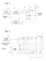
- FIG 2 shows the voltage regulator arrangement which is the heart of the power control design.
- the regulator output voltage is controlled via a feedback loop tied to the scaled replica cell 8.
- the regulator output voltage is adjusted until the current kI REF flowing through the replica is at the desired level.
- This method causes related currents (I A , I B , ..., I M ) to flow through the amplifier core (see in Figure 3 ). Strictly speaking this controls the output current rather than the output power.
- P I 2 * R, therefore the output power is indirectly controlled if a proper chosen load resistance is used.
- a conversion factor is used because the current through the replica cell is a DC current and the current at the power amplifier output is an RMS current.
- the regulator 12 namely in this example a voltage comparator, is used to fix the voltage at the top of the replica cell 8 to a selected reference voltage V REF provided by the voltage generator 11. Additionally the current generator 9 is used to provide a selected current I REF for the replica cell.
- the power controller 12 is used to adjust both the selected voltage reference and the selected current reference.
- the output of the regulator voltage known as the regulator output voltage is then distributed to provide the supply voltage for the preamplifier inverters 3a-3m as will be shown in Figure 3 .
- the main power control is accomplished by switching in parallel a combination of selected amplifier cells to define a rough attenuation.
- the current generator advantageously delivers several different current levels, e.g. four current levels, under request of the power controller allowing such fine attenuation step, e.g. 1dB increment.
- the power amplifier output signal may be attenuated in a fine stepwise manner, in this example by 4dB with 1 dB step, by controlling the current flowing through the replica device so that it causes the regulator voltage to adjust its output voltage until it equalizes this current.
- this current level adjusts the supply voltage reference for the inverters.
- the replica cell is advantageously a cascoded driver comprising two transistors N1 and N2 connected in a cascode arrangement where transistor N1 is present to limit the voltage on N2.
- the current flowing through the replica cell corresponds to the reference current mirrored in a current mirror 13 with an adequate coefficient k.
- Minimum channel length transistors are both used for the replica cell and the similar cells in the amplifier core to allow the highest frequency operation.
- these cascoded drivers exhibit poor output impedance and thus the voltage on the drain of the top of each cell affects the current flowing through and cause it varies based on the source to drain voltage, which consequently affects the output power.
- the voltage regulator output controls the gate of transistor N2 of the replica in function of the comparison between the voltage at the top of the replica cell and the voltage reference.
- the amplifier adjusts the gate level of the replica until the voltage at the source of the replica cascode is equal to the generated voltage level of the voltage generator. This arrangement eliminates the current variations caused by the voltage present at the source of the cascode.
- This DC voltage is advantageously designed to approximate the lowest voltage seen at the power amplifier output for a given power setting. This corrects for a second order effect the output impedance.
- the first factor is the current ratio flowing through the amplifier core controlled by the power controller for attenuating the power of the output signal and advantageously use of a variable current generator for a fine attenuation. This first factor allows better power control because the current variations due to the source to drain voltage are dramatically reduced.
- the second factor is the voltage generator used for fixing the output voltage of the replica cell further which allows approximating the RMS voltage present at the power amplifier output.
- FIG. 3 it shows the amplifier core arrangement.
- the regulator output from Figure 2 is applied to the drive unit 3 constituted by inverter preamplifier(s) which in turn sets the maximum gate drive voltage.
- the drive unit 3 constituted by inverter preamplifier(s) which in turn sets the maximum gate drive voltage.
- the gate drive voltage As temperature, process parameters, etc. change the drive voltage level, the gate drive voltage also changes to lessen their effects.
- inverters of the drive unit 3 driven by the regulator output along with the power controller instructions are used in turn to drive the gates of the parallel cascoded drivers of the amplifier core 1.
- each selected cell namely the different cascoded drivers (A,B,C,D, E1-E4)
- the different cascoded drivers A,B,C,D, E1-E4
- 4dB attenuation is already controlled by the current level (i.e. gate drive) as explained in relation with Figure 2 .
- each selected combination allows 4dB step attenuation by switching in or out the drivers.
- an adequate number of amplifier cells with adequate ratios is chosen.
- One advantageous implementation includes one 4X driver (A), two 2X drivers (B and C), one 1X driver (D) and one 1 ⁇ 2 X driver (E1), one 1 ⁇ 4 X driver (E2) and two 1/8 X drivers (E3 and E4), where X corresponds to the number of times the reference current flows in each of the driver blocks (I A through I E4 ).
- the output power is then related to the sum of currents flowing through the activated cells multiplied by the scaling size inverse.
- Attenuation control with a codeword controlled by the power controller where the three first bits correspond to a rough attenuation (e.g. with a 4dB step) obtained with different combinations of activated cells, and the last two bits correspond to a fine attenuation (e.g. with a 1dB step) obtained with different reference current levels.
- a rough attenuation e.g. with a 4dB step
- a fine attenuation e.g. with a 1dB step
- Attenuation dB Codeword Implemented ratio Activated cells Current level Error % 0 00000 10 All cells Max 0 1 000 01 10 All cells Next to max 0 2 000 10 10 All cells Next to min 0 3 000 11 10 All cells Min 0 4 001 00 6.25 A, B, E1, E2 Max -0.8 8 010 00 4 A or B, C Max 0 15 011 11 2.5 B, E1 Min 0 24 110 00 0.625 E1, E3 Max -0,8 31 111 11 0.375 E2, E4 Min -6.2
- the output of the regulator adjusts to hold a specific voltage at the source of N1. It is done by adjusting the gate voltage on N2 until it sinks the exact amount of current provided by the reference current.
- the reference voltage is required to compensate the output impedance of the drive transistors of each amplifier cells (N1 etc).
- this invention allows for accurate power control steps, in this case 1 dB.
- This control structure attempts to remove power fluctuations caused by process parameters, supply voltage reference, and temperature variations while providing a wide dynamic range of power control, in this case 32dB.
Landscapes
- Engineering & Computer Science (AREA)
- Power Engineering (AREA)
- Amplifiers (AREA)
Abstract
Description
- The present invention generally relates to RF power devices, in particular to power amplifiers with a controlled output power.
- Product manufacturers have a need to control output power from RF power devices. This allows them to optimize performances such as transmission range and battery life and at the same time not to violate government regulations dealing with power emissions. For that purpose, power amplifiers known in the art are usually based on methods that control gate or base drive, adjust bias current or parallel devices together to perform power control.
- Nevertheless existing power amplifier control techniques are sensitive to temperature, manufacturing process tolerances and power supply voltage variations.
- One goal of the present invention is thus to carry out a reliable and simple controlled power amplifier which overcomes the drawbacks of the prior art. For that purpose, it is provided with power control by controlling DC current in a replica device as well as using parallel devices to obtain a stepwise power control. The power amplifier according to the present invention therefore comprises an amplifier core including parallel amplifier cells, a replica cell made of one amplifier cell similar to those of the amplifier core, a power controller to select a combination of amplifier cells to activate, a regulator to fix the top voltage of the replica cell to a reference voltage, a voltage generator to provide the voltage reference to the regulator, a current generator to provide a reference current through the replica cell and a drive unit controlled by the regulator output to drive the combination of amplifier cells, wherein each selected combination of activated cells defines a predetermined attenuation level of power amplifier output signal so that it is attenuated in a stepwise manner. Thus temperature, manufacturing process tolerances and power supply voltage variations may be all minimized.
- According to an advantageous embodiment, the power controller selects the reference current between a defined number of current levels to attenuate said power amplifier output signal with a corresponding number of attenuation levels.
- According to another advantageous embodiment, combinations of activated cells define rough attenuation steps and each current level of said current reference defines a fine attenuation step.
- Other advantageous embodiments of the power amplifier form the subject of the dependent claims.
- Another object of the present invention concerns a method to control the power output of a power amplifier.
- Other aspects, features and advantages of the present invention will be apparent upon reading the following detailed description of non-limiting examples and embodiments made with reference to the accompanying drawings.
-
Figure 1 shows the overall block diagram of the power amplifier; -
Figure 2 shows the voltage regulator arrangement; -
Figure 3 shows the power amplifier core arrangement. - The following description of a power amplifier with control output power is given by way of a non limiting example in relation with
Figures 1 to 3 . -
Figure 1 shows the overall block diagram of the power amplifier according to a preferred embodiment of the invention. Thepower amplifier core 1 consists inparallel amplifier cells 2a-2m, preferably cascoded amplifiers or as labelled "cascoded drivers" each being controlled by the means of acorresponding drive gate 3a-3m. When operating theamplifier core 1 functions as a class C type amplifier by pulling current from a load during a portion of one period of the output frequency, e.g. an antenna 4 connected at the terminals of a Current-Mode Logic tofull swing unit 5 connected in turn toinverters 6a-6m to distribute the pulled load to amplifiercore 1 viadrive gates 3a-3m. The current pulled from load 4 may be controlled by the amplitude and/or width of the pulse on thedrive gate 3a-3m ofcascoded drivers 2a-2m. In fact, in this circuit the output power is advantageously controlled both by the number ofcascoded drivers 2a-2m activated in parallel and the amount of driver's gate drive. It is to be noted that in the represented example, no specific means have been implemented to control the gate pulse width, but they could however be implemented to give another adjustment parameter of the power output. At the output of theamplifier core 1, it is preferably provided with an ESD protection circuit to prevent electrostatic discharge. - The main idea behind the present invention is to use a scaled
replica cell 8, similar to any ofamplifier cells 2a-2m of the amplifier core, in order to sink current from acurrent source 9. By monitoring and controlling the current through replica cell 8 a proportional current is to be expected to flow throughamplifier core 1, namely the cascoded drivers. This is accomplished by using a feedback circuit around the replica that will be explained in more detailed in liaison withFigure 2 . This feedback loop comprises avoltage regulator 10 to fix the top voltage ofreplica cell 8 to a reference voltage provided by avoltage generator 11. - In order to obtain the desired attenuation level at the power amplifier output, a
power controller 12 selects a combination of amplifier cells to activate. The desired power level is determined by a codeword which defines the combination ofamplifier cells 2a-2m to be activated and adjustments of the current and voltage references if needed. Each combination of activated amplifier cells defines a predetermined attenuation level of the power amplifier output signal so that it may be attenuated in a stepwise manner according to the selected combination. - As already mentioned above, a drive unit 3 including
drive gates 3a-3m, e.g. inverters, connected to corresponding cascoded drivers is controlled by the regulator output to drive the amplifier cells. This is accomplished by using the regulator output as the voltage source of the inverters of drive unit 3 that are used to drive the cascoded drivers. Advantageously, as it will be explained later on, the current reference may be programmed bypower controller 12 with a defined number of current levels in order to finely attenuate the power amplifier output signal with a corresponding number of attenuation levels. - Thus, it is advantageously first combinations of activated cells for defining rough attenuation steps and several current levels of the current reference for defining fine attenuation steps. Furthermore, the power controller may adjust the reference voltage to compensate voltage variations at the power amplifier output. Another power control may be achieved by controlling the level of the voltage swing on the drive gates of the amplifier core. This is accomplished by controlling the output voltage of the regulator that is used to provide the supply voltage to the inverters also used as preamplifiers. This effectively causes the output signal swing of these inverters to toggle between ground and the regulator output voltage level.
- One will now describe how the power control of such a power amplifier works in view of
Figures 2 and 3 showing the voltage regulator arrangement, respectively, the amplifier core arrangement. -
Figure 2 shows the voltage regulator arrangement which is the heart of the power control design. The regulator output voltage is controlled via a feedback loop tied to the scaledreplica cell 8. The regulator output voltage is adjusted until the current kIREF flowing through the replica is at the desired level. This method causes related currents (IA, IB, ..., IM) to flow through the amplifier core (see inFigure 3 ). Strictly speaking this controls the output current rather than the output power. However since current and power are related according to the following expression P = I2 * R, therefore the output power is indirectly controlled if a proper chosen load resistance is used. It is to note that a conversion factor is used because the current through the replica cell is a DC current and the current at the power amplifier output is an RMS current. - The
regulator 12, namely in this example a voltage comparator, is used to fix the voltage at the top of thereplica cell 8 to a selected reference voltage VREF provided by thevoltage generator 11. Additionally thecurrent generator 9 is used to provide a selected current IREF for the replica cell. Thepower controller 12 is used to adjust both the selected voltage reference and the selected current reference. The output of the regulator voltage known as the regulator output voltage is then distributed to provide the supply voltage for thepreamplifier inverters 3a-3m as will be shown inFigure 3 . As already mentioned and will be seen later on again, the main power control is accomplished by switching in parallel a combination of selected amplifier cells to define a rough attenuation. In addition, to more finely adjust the attenuation of the power amplifier output signal, the current generator advantageously delivers several different current levels, e.g. four current levels, under request of the power controller allowing such fine attenuation step, e.g. 1dB increment. Thus the power amplifier output signal may be attenuated in a fine stepwise manner, in this example by 4dB with 1 dB step, by controlling the current flowing through the replica device so that it causes the regulator voltage to adjust its output voltage until it equalizes this current. In summary this current level adjusts the supply voltage reference for the inverters. - In the represented example, the replica cell is advantageously a cascoded driver comprising two transistors N1 and N2 connected in a cascode arrangement where transistor N1 is present to limit the voltage on N2. The current flowing through the replica cell corresponds to the reference current mirrored in a
current mirror 13 with an adequate coefficient k. - Minimum channel length transistors are both used for the replica cell and the similar cells in the amplifier core to allow the highest frequency operation. However, these cascoded drivers exhibit poor output impedance and thus the voltage on the drain of the top of each cell affects the current flowing through and cause it varies based on the source to drain voltage, which consequently affects the output power. Thus, in order to minimize this effect the feedback path around the replica cell not only controls the current through the replica but also the voltage on the drain of transistor N1. The voltage regulator output controls the gate of transistor N2 of the replica in function of the comparison between the voltage at the top of the replica cell and the voltage reference. The amplifier adjusts the gate level of the replica until the voltage at the source of the replica cascode is equal to the generated voltage level of the voltage generator. This arrangement eliminates the current variations caused by the voltage present at the source of the cascode. This DC voltage is advantageously designed to approximate the lowest voltage seen at the power amplifier output for a given power setting. This corrects for a second order effect the output impedance.
- Therefore there are two main factors that are used to set the output power. The first factor is the current ratio flowing through the amplifier core controlled by the power controller for attenuating the power of the output signal and advantageously use of a variable current generator for a fine attenuation. This first factor allows better power control because the current variations due to the source to drain voltage are dramatically reduced. The second factor is the voltage generator used for fixing the output voltage of the replica cell further which allows approximating the RMS voltage present at the power amplifier output.
- Finally referring to
Figure 2 , it is to be noted that in the represented embodiment the reference current and reference voltage are generated internally using a bandgap reference. However, another method would be to use an external resistor for example to obtain a more precise and/or flexible solution. - Turning now to
Figure 3 , it shows the amplifier core arrangement. The regulator output fromFigure 2 is applied to the drive unit 3 constituted by inverter preamplifier(s) which in turn sets the maximum gate drive voltage. As temperature, process parameters, etc. change the drive voltage level, the gate drive voltage also changes to lessen their effects. Actually, as shown, inverters of the drive unit 3 driven by the regulator output along with the power controller instructions are used in turn to drive the gates of the parallel cascoded drivers of theamplifier core 1. - According to the power controller instruction used to turn on and off each selected cells, namely the different cascoded drivers (A,B,C,D, E1-E4), to be activated or deactivated so that its achieves a defined combination of amplifier cells with the desired power. In the represented preferred embodiment, 4dB attenuation is already controlled by the current level (i.e. gate drive) as explained in relation with
Figure 2 . Then each selected combination allows 4dB step attenuation by switching in or out the drivers. However, it should be noticed that it is also possible to divide the current control versus combination of parallel drivers in a different ratio than four to one. - According to the desired overall power amplification, an adequate scaling size is chosen between the replica cell and the number of parallel drivers. This choice should take into account the fact that the output power is related to the reference current and the scale factor according to the following expression:

- Further, according to the desired attenuation range, for instance for an attenuation range of 32dB, an adequate number of amplifier cells with adequate ratios is chosen. One advantageous implementation includes one 4X driver (A), two 2X drivers (B and C), one 1X driver (D) and one ½ X driver (E1), one ¼ X driver (E2) and two 1/8 X drivers (E3 and E4), where X corresponds to the number of times the reference current flows in each of the driver blocks (IA through IE4). The output power is then related to the sum of currents flowing through the activated cells multiplied by the scaling size inverse.
- Below is given one example of attenuation control with a codeword controlled by the power controller where the three first bits correspond to a rough attenuation (e.g. with a 4dB step) obtained with different combinations of activated cells, and the last two bits correspond to a fine attenuation (e.g. with a 1dB step) obtained with different reference current levels.
Attenuation dB Codeword Implemented ratio Activated cells Current level Error % 0 00000 10 All cells Max 0 1 000 01 10 All cells Next to max 0 2 000 10 10 All cells Next to min 0 3 000 11 10 All cells Min 0 4 001 00 6.25 A, B, E1, E2 Max -0.8 8 010 00 4 A or B, C Max 0 15 011 11 2.5 B, E1 Min 0 24 110 00 0.625 E1, E3 Max -0,8 31 111 11 0.375 E2, E4 Min -6.2 - It should be also noted that, the output of the regulator adjusts to hold a specific voltage at the source of N1. It is done by adjusting the gate voltage on N2 until it sinks the exact amount of current provided by the reference current. The reference voltage is required to compensate the output impedance of the drive transistors of each amplifier cells (N1 etc).
- As stated above, this invention allows for accurate power control steps, in this
case 1 dB. This control structure attempts to remove power fluctuations caused by process parameters, supply voltage reference, and temperature variations while providing a wide dynamic range of power control, in this case 32dB. - Having described the invention with regard to certain specific embodiments, it is to be understood that these embodiments are not meant as limitations of the invention. Indeed, various modifications and/or adaptations may become apparent to those skilled in the art without departing from the scope of the annexed claims.
Claims (13)
- A power amplifier comprises:- an amplifier core including parallel amplifier cells;- a replica cell made of one amplifier cell similar to those of said amplifier core;- a power controller to select a combination of amplifier cells to activate;- a regulator to fix a top voltage of said replica cell to a reference voltage;- a voltage generator to provide said voltage reference to said regulator;- a current generator to provide a reference current through said replica cell; and- a drive unit controlled by said regulator output to drive said combination of amplifier cells,wherein each selected combination of activated amplifier cells defines a predetermined attenuation level of power amplifier output signal so that it is attenuated in a stepwise manner.
- The power amplifier of claim 1, wherein said power controller selects said reference current between a defined number of current levels to attenuate said power amplifier output signal with a corresponding number of attenuation levels.
- The power amplifier of claim 2, wherein combinations of activated cells define rough attenuation steps and each current level of said current reference defines a fine attenuation step.
- The power amplifier of claim 3, wherein said reference current is selected between n current levels to attenuate said power amplifier output signal by step of one decibel with respectively n attenuation levels.
- The power amplifier of claim 4, wherein said amplifier core comprises different combinations of amplifier cells defining a number of different attenuation levels by step of n decibels of said power output signal.
- The power amplifier of claim 1, wherein said power controller switches in amplifier cells of said combination and switches out amplifier cells which are not part of said combination.
- The power amplifier of claim 1, wherein said amplifier cells are cascoded drivers.
- The power amplifier of claim 1, wherein said regulator is a voltage comparator receiving at its inputs said top voltage of the replica cell and said reference voltage so that it delivers a regulator output voltage limiting excursion of said drive unit.
- The power amplifier of claim 8, wherein said drive unit comprises inverters to drive said amplifier cells.
- The power amplifier of claim 1, wherein said power controller selects said reference voltage to compensate voltage variations at the power amplifier output.
- A method to control power amplifier output of a power amplifier comprising an amplifier core including parallel amplifier cells, a replica cell made of one amplifier cell similar to those of said amplifier core, wherein the method comprises the steps of:- providing a reference voltage by means of voltage generator,- providing a reference current through the replica cell by means of a current generator,- fixing a top voltage of said replica cell to said reference voltage by means of a regulator;- selecting a combination of amplifier cells to be activated by means of a power controller,- driving the selected combination of amplifier cells by means of a drive unit controlled by said regulator,- attenuating in a stepwise manner level of power amplifier output signal by means of the selected combination of amplifier cells.
- The method of claim 11, wherein it further comprises the step of- selecting said reference current between a defined number of current levels by means of the power controller,- attenuating said power amplifier output signal with a corresponding number of attenuation levels.
- The method of claim 12, wherein combinations of activated cells define rough attenuation steps and each current level of said current reference defines a fine attenuation step.
Applications Claiming Priority (1)
| Application Number | Priority Date | Filing Date | Title |
|---|---|---|---|
| US11/745,891 US7560989B2 (en) | 2007-05-08 | 2007-05-08 | Power amplifier with controlled output power |
Publications (2)
| Publication Number | Publication Date |
|---|---|
| EP1993200A1 true EP1993200A1 (en) | 2008-11-19 |
| EP1993200B1 EP1993200B1 (en) | 2011-08-03 |
Family
ID=39705162
Family Applications (1)
| Application Number | Title | Priority Date | Filing Date |
|---|---|---|---|
| EP08155904A Active EP1993200B1 (en) | 2007-05-08 | 2008-05-08 | Power amplifier with controlled output power |
Country Status (2)
| Country | Link |
|---|---|
| US (1) | US7560989B2 (en) |
| EP (1) | EP1993200B1 (en) |
Cited By (2)
| Publication number | Priority date | Publication date | Assignee | Title |
|---|---|---|---|---|
| EP2482449A1 (en) * | 2011-01-27 | 2012-08-01 | ST-Ericsson SA | Amplification circuit having optimization of power |
| EP3251210A1 (en) * | 2015-03-30 | 2017-12-06 | Siemens Aktiengesellschaft | Transmission amplifier for amplifying a signal in a wire-free transmission system |
Families Citing this family (2)
| Publication number | Priority date | Publication date | Assignee | Title |
|---|---|---|---|---|
| US8380147B2 (en) | 2011-04-05 | 2013-02-19 | Em Microelectronic-Marin S.A. | Power amplifier circuit with means for tuning wave shape of ASK RF signal envelope, and method for implementing the power amplifier circuit |
| EP2608401B1 (en) | 2011-12-21 | 2019-03-27 | EM Microelectronic-Marin SA | Circuit for transmitting ASK RF signals with adaptation of the edges of the data signals |
Citations (4)
| Publication number | Priority date | Publication date | Assignee | Title |
|---|---|---|---|---|
| US6181206B1 (en) * | 1998-06-23 | 2001-01-30 | Stmicroelectronics S.R.L. | Low noise RF amplifier with programmable gain |
| US20060119435A1 (en) * | 2004-12-02 | 2006-06-08 | Hyoung-Seok Oh | Triple cascode power amplifier of inner parallel configuration with dynamic gate bias technique |
| US20070096827A1 (en) * | 2005-11-02 | 2007-05-03 | Nguyen Cuong Q | Multi controlled output levels cmos power amplifier (pa) |
| EP1837989A1 (en) * | 2006-03-24 | 2007-09-26 | Sharp Kabushiki Kaisha | Variable gain amplifier |
Family Cites Families (2)
| Publication number | Priority date | Publication date | Assignee | Title |
|---|---|---|---|---|
| JP4154910B2 (en) * | 2002-03-29 | 2008-09-24 | 沖電気工業株式会社 | Distributed amplifier |
| KR100821197B1 (en) * | 2005-10-17 | 2008-04-11 | 한국전자통신연구원 | High Efficiency Mixed Mode Power Amplifiers |
-
2007
- 2007-05-08 US US11/745,891 patent/US7560989B2/en active Active
-
2008
- 2008-05-08 EP EP08155904A patent/EP1993200B1/en active Active
Patent Citations (4)
| Publication number | Priority date | Publication date | Assignee | Title |
|---|---|---|---|---|
| US6181206B1 (en) * | 1998-06-23 | 2001-01-30 | Stmicroelectronics S.R.L. | Low noise RF amplifier with programmable gain |
| US20060119435A1 (en) * | 2004-12-02 | 2006-06-08 | Hyoung-Seok Oh | Triple cascode power amplifier of inner parallel configuration with dynamic gate bias technique |
| US20070096827A1 (en) * | 2005-11-02 | 2007-05-03 | Nguyen Cuong Q | Multi controlled output levels cmos power amplifier (pa) |
| EP1837989A1 (en) * | 2006-03-24 | 2007-09-26 | Sharp Kabushiki Kaisha | Variable gain amplifier |
Cited By (5)
| Publication number | Priority date | Publication date | Assignee | Title |
|---|---|---|---|---|
| EP2482449A1 (en) * | 2011-01-27 | 2012-08-01 | ST-Ericsson SA | Amplification circuit having optimization of power |
| WO2012100947A1 (en) * | 2011-01-27 | 2012-08-02 | St-Ericsson Sa | Amplification circuit having optimization of power |
| US9166527B2 (en) | 2011-01-27 | 2015-10-20 | St-Ericsson Sa | Amplification circuit having optimization of power |
| EP3499713A1 (en) * | 2011-01-27 | 2019-06-19 | Telefonaktiebolaget LM Ericsson (publ) | Amplification circuit having optimization of power |
| EP3251210A1 (en) * | 2015-03-30 | 2017-12-06 | Siemens Aktiengesellschaft | Transmission amplifier for amplifying a signal in a wire-free transmission system |
Also Published As
| Publication number | Publication date |
|---|---|
| US7560989B2 (en) | 2009-07-14 |
| EP1993200B1 (en) | 2011-08-03 |
| US20080278239A1 (en) | 2008-11-13 |
Similar Documents
| Publication | Publication Date | Title |
|---|---|---|
| EP1461923B1 (en) | Low supply voltage differential signal driver | |
| US6288564B1 (en) | Line receiver circuit with line termination impedance | |
| US6011437A (en) | High precision, high bandwidth variable gain amplifier and method | |
| KR101912490B1 (en) | Integrated start-up bias boost for dynamic error vector magnitude enhancement | |
| US7795942B2 (en) | Stage by stage delay current-summing slew rate controller | |
| US20050275394A1 (en) | Current-limiting circuitry | |
| US20040222821A1 (en) | Series terminated CMOS output driver with impedance calibration | |
| JP2003069415A (en) | Method of controlling slew rate of transition edge of digital signal at node of integrated circuit | |
| KR20190010684A (en) | Adaptive multi-band bias control circuit and power amplifier apparatus | |
| CN110350881B (en) | Attenuator system | |
| EP1993200B1 (en) | Power amplifier with controlled output power | |
| US7656227B1 (en) | Techniques to control amplifier gain over process, voltage, and/or temperature (PVT) variations | |
| US20220353970A1 (en) | Current control circuitry | |
| US8410824B2 (en) | Buffer with active output impedance matching | |
| EP0545536B1 (en) | Voltage-controlled amplifier using operational amplifier | |
| EP2030319B1 (en) | Digital attenuator circuits and methods for use thereof | |
| US7362172B2 (en) | Variable gain circuit | |
| US6937071B1 (en) | High frequency differential power amplifier | |
| WO2011023210A1 (en) | Adjustable gain amplifier, automated test equipment and method for adjusting a gain of an amplifier | |
| US20180062596A1 (en) | Linear-in-dB, Low-Voltage, Programmable/Variable Gain Amplifier (PGA) Using Recursive Current Division | |
| US8139789B2 (en) | Signal amplifier circuit | |
| US20060057982A1 (en) | Transmission apparatus and mobile communication terminal apparatus | |
| US11677360B2 (en) | Equalization in a multi-path audio amplifier for canceling variations due to multi-path output impedance differences | |
| US20060202756A1 (en) | Radio-frequency power amplifier apparatus and method of adjusting output power thereof | |
| US6724251B1 (en) | Apparatus and method for employing gain dependent biasing to reduce offset and noise in a current conveyor type amplifier |
Legal Events
| Date | Code | Title | Description |
|---|---|---|---|
| PUAI | Public reference made under article 153(3) epc to a published international application that has entered the european phase |
Free format text: ORIGINAL CODE: 0009012 |
|
| AK | Designated contracting states |
Kind code of ref document: A1 Designated state(s): AT BE BG CH CY CZ DE DK EE ES FI FR GB GR HR HU IE IS IT LI LT LU LV MC MT NL NO PL PT RO SE SI SK TR |
|
| AX | Request for extension of the european patent |
Extension state: AL BA MK RS |
|
| 17P | Request for examination filed |
Effective date: 20090519 |
|
| AKX | Designation fees paid |
Designated state(s): CH DE FR LI |
|
| GRAP | Despatch of communication of intention to grant a patent |
Free format text: ORIGINAL CODE: EPIDOSNIGR1 |
|
| GRAS | Grant fee paid |
Free format text: ORIGINAL CODE: EPIDOSNIGR3 |
|
| GRAA | (expected) grant |
Free format text: ORIGINAL CODE: 0009210 |
|
| AK | Designated contracting states |
Kind code of ref document: B1 Designated state(s): CH DE FR LI |
|
| REG | Reference to a national code |
Ref country code: CH Ref legal event code: EP Ref country code: CH Ref legal event code: NV Representative=s name: ICB INGENIEURS CONSEILS EN BREVETS SA |
|
| REG | Reference to a national code |
Ref country code: DE Ref legal event code: R096 Ref document number: 602008008564 Country of ref document: DE Effective date: 20111006 |
|
| PLBE | No opposition filed within time limit |
Free format text: ORIGINAL CODE: 0009261 |
|
| STAA | Information on the status of an ep patent application or granted ep patent |
Free format text: STATUS: NO OPPOSITION FILED WITHIN TIME LIMIT |
|
| 26N | No opposition filed |
Effective date: 20120504 |
|
| REG | Reference to a national code |
Ref country code: DE Ref legal event code: R097 Ref document number: 602008008564 Country of ref document: DE Effective date: 20120504 |
|
| REG | Reference to a national code |
Ref country code: FR Ref legal event code: PLFP Year of fee payment: 9 |
|
| REG | Reference to a national code |
Ref country code: FR Ref legal event code: PLFP Year of fee payment: 10 |
|
| REG | Reference to a national code |
Ref country code: FR Ref legal event code: PLFP Year of fee payment: 11 |
|
| P01 | Opt-out of the competence of the unified patent court (upc) registered |
Effective date: 20230611 |
|
| PGFP | Annual fee paid to national office [announced via postgrant information from national office to epo] |
Ref country code: DE Payment date: 20240418 Year of fee payment: 17 |
|
| PGFP | Annual fee paid to national office [announced via postgrant information from national office to epo] |
Ref country code: FR Payment date: 20250423 Year of fee payment: 18 |
|
| PGFP | Annual fee paid to national office [announced via postgrant information from national office to epo] |
Ref country code: CH Payment date: 20250601 Year of fee payment: 18 |
|
| REG | Reference to a national code |
Ref country code: DE Ref legal event code: R119 Ref document number: 602008008564 Country of ref document: DE |
|
| PG25 | Lapsed in a contracting state [announced via postgrant information from national office to epo] |
Ref country code: DE Free format text: LAPSE BECAUSE OF NON-PAYMENT OF DUE FEES Effective date: 20251202 |