EP1993148A1 - Optical transmission/reception device - Google Patents
Optical transmission/reception device Download PDFInfo
- Publication number
- EP1993148A1 EP1993148A1 EP07714226A EP07714226A EP1993148A1 EP 1993148 A1 EP1993148 A1 EP 1993148A1 EP 07714226 A EP07714226 A EP 07714226A EP 07714226 A EP07714226 A EP 07714226A EP 1993148 A1 EP1993148 A1 EP 1993148A1
- Authority
- EP
- European Patent Office
- Prior art keywords
- light
- wire
- base substrate
- receiving device
- optical transmitting
- Prior art date
- Legal status (The legal status is an assumption and is not a legal conclusion. Google has not performed a legal analysis and makes no representation as to the accuracy of the status listed.)
- Withdrawn
Links
- 230000003287 optical effect Effects 0.000 title claims abstract description 51
- 230000005540 biological transmission Effects 0.000 title 1
- 239000000758 substrate Substances 0.000 claims abstract description 57
- 238000009751 slip forming Methods 0.000 claims description 3
- 239000002585 base Substances 0.000 description 37
- 230000017531 blood circulation Effects 0.000 description 9
- 239000000463 material Substances 0.000 description 9
- 239000004065 semiconductor Substances 0.000 description 6
- XUIMIQQOPSSXEZ-UHFFFAOYSA-N Silicon Chemical compound [Si] XUIMIQQOPSSXEZ-UHFFFAOYSA-N 0.000 description 5
- 229910052710 silicon Inorganic materials 0.000 description 5
- 239000010703 silicon Substances 0.000 description 5
- VYPSYNLAJGMNEJ-UHFFFAOYSA-N Silicium dioxide Chemical compound O=[Si]=O VYPSYNLAJGMNEJ-UHFFFAOYSA-N 0.000 description 4
- 230000000694 effects Effects 0.000 description 4
- 229920005989 resin Polymers 0.000 description 4
- 239000011347 resin Substances 0.000 description 4
- 229910018885 Pt—Au Inorganic materials 0.000 description 2
- 210000004369 blood Anatomy 0.000 description 2
- 239000008280 blood Substances 0.000 description 2
- 229910052681 coesite Inorganic materials 0.000 description 2
- 238000010276 construction Methods 0.000 description 2
- 229910052906 cristobalite Inorganic materials 0.000 description 2
- 239000000377 silicon dioxide Substances 0.000 description 2
- 229910000679 solder Inorganic materials 0.000 description 2
- 229910052682 stishovite Inorganic materials 0.000 description 2
- 229910052905 tridymite Inorganic materials 0.000 description 2
- OKTJSMMVPCPJKN-UHFFFAOYSA-N Carbon Chemical compound [C] OKTJSMMVPCPJKN-UHFFFAOYSA-N 0.000 description 1
- 229910001218 Gallium arsenide Inorganic materials 0.000 description 1
- 229910000530 Gallium indium arsenide Inorganic materials 0.000 description 1
- 229910007637 SnAg Inorganic materials 0.000 description 1
- 239000003513 alkali Substances 0.000 description 1
- 239000005388 borosilicate glass Substances 0.000 description 1
- 229910052799 carbon Inorganic materials 0.000 description 1
- 150000001875 compounds Chemical class 0.000 description 1
- 229910052802 copper Inorganic materials 0.000 description 1
- 238000001312 dry etching Methods 0.000 description 1
- 210000003743 erythrocyte Anatomy 0.000 description 1
- 238000005530 etching Methods 0.000 description 1
- 239000000945 filler Substances 0.000 description 1
- 239000012530 fluid Substances 0.000 description 1
- 229910052737 gold Inorganic materials 0.000 description 1
- 230000001678 irradiating effect Effects 0.000 description 1
- 238000005259 measurement Methods 0.000 description 1
- 229910052759 nickel Inorganic materials 0.000 description 1
- 230000003647 oxidation Effects 0.000 description 1
- 238000007254 oxidation reaction Methods 0.000 description 1
- 229920002050 silicone resin Polymers 0.000 description 1
- 239000000126 substance Substances 0.000 description 1
- 238000001039 wet etching Methods 0.000 description 1
Images


Classifications
-
- H—ELECTRICITY
- H01—ELECTRIC ELEMENTS
- H01L—SEMICONDUCTOR DEVICES NOT COVERED BY CLASS H10
- H01L31/00—Semiconductor devices sensitive to infrared radiation, light, electromagnetic radiation of shorter wavelength or corpuscular radiation and specially adapted either for the conversion of the energy of such radiation into electrical energy or for the control of electrical energy by such radiation; Processes or apparatus specially adapted for the manufacture or treatment thereof or of parts thereof; Details thereof
- H01L31/02—Details
- H01L31/0203—Containers; Encapsulations, e.g. encapsulation of photodiodes
-
- H—ELECTRICITY
- H01—ELECTRIC ELEMENTS
- H01L—SEMICONDUCTOR DEVICES NOT COVERED BY CLASS H10
- H01L31/00—Semiconductor devices sensitive to infrared radiation, light, electromagnetic radiation of shorter wavelength or corpuscular radiation and specially adapted either for the conversion of the energy of such radiation into electrical energy or for the control of electrical energy by such radiation; Processes or apparatus specially adapted for the manufacture or treatment thereof or of parts thereof; Details thereof
- H01L31/02—Details
-
- A—HUMAN NECESSITIES
- A61—MEDICAL OR VETERINARY SCIENCE; HYGIENE
- A61B—DIAGNOSIS; SURGERY; IDENTIFICATION
- A61B5/00—Measuring for diagnostic purposes; Identification of persons
- A61B5/02—Detecting, measuring or recording pulse, heart rate, blood pressure or blood flow; Combined pulse/heart-rate/blood pressure determination; Evaluating a cardiovascular condition not otherwise provided for, e.g. using combinations of techniques provided for in this group with electrocardiography or electroauscultation; Heart catheters for measuring blood pressure
- A61B5/024—Detecting, measuring or recording pulse rate or heart rate
- A61B5/0245—Detecting, measuring or recording pulse rate or heart rate by using sensing means generating electric signals, i.e. ECG signals
-
- A—HUMAN NECESSITIES
- A61—MEDICAL OR VETERINARY SCIENCE; HYGIENE
- A61B—DIAGNOSIS; SURGERY; IDENTIFICATION
- A61B5/00—Measuring for diagnostic purposes; Identification of persons
- A61B5/02—Detecting, measuring or recording pulse, heart rate, blood pressure or blood flow; Combined pulse/heart-rate/blood pressure determination; Evaluating a cardiovascular condition not otherwise provided for, e.g. using combinations of techniques provided for in this group with electrocardiography or electroauscultation; Heart catheters for measuring blood pressure
- A61B5/026—Measuring blood flow
- A61B5/0261—Measuring blood flow using optical means, e.g. infrared light
-
- H—ELECTRICITY
- H01—ELECTRIC ELEMENTS
- H01L—SEMICONDUCTOR DEVICES NOT COVERED BY CLASS H10
- H01L2224/00—Indexing scheme for arrangements for connecting or disconnecting semiconductor or solid-state bodies and methods related thereto as covered by H01L24/00
- H01L2224/01—Means for bonding being attached to, or being formed on, the surface to be connected, e.g. chip-to-package, die-attach, "first-level" interconnects; Manufacturing methods related thereto
- H01L2224/42—Wire connectors; Manufacturing methods related thereto
- H01L2224/44—Structure, shape, material or disposition of the wire connectors prior to the connecting process
- H01L2224/45—Structure, shape, material or disposition of the wire connectors prior to the connecting process of an individual wire connector
- H01L2224/45001—Core members of the connector
- H01L2224/45099—Material
- H01L2224/451—Material with a principal constituent of the material being a metal or a metalloid, e.g. boron (B), silicon (Si), germanium (Ge), arsenic (As), antimony (Sb), tellurium (Te) and polonium (Po), and alloys thereof
- H01L2224/45138—Material with a principal constituent of the material being a metal or a metalloid, e.g. boron (B), silicon (Si), germanium (Ge), arsenic (As), antimony (Sb), tellurium (Te) and polonium (Po), and alloys thereof the principal constituent melting at a temperature of greater than or equal to 950°C and less than 1550°C
- H01L2224/45139—Silver (Ag) as principal constituent
-
- H—ELECTRICITY
- H01—ELECTRIC ELEMENTS
- H01L—SEMICONDUCTOR DEVICES NOT COVERED BY CLASS H10
- H01L2224/00—Indexing scheme for arrangements for connecting or disconnecting semiconductor or solid-state bodies and methods related thereto as covered by H01L24/00
- H01L2224/01—Means for bonding being attached to, or being formed on, the surface to be connected, e.g. chip-to-package, die-attach, "first-level" interconnects; Manufacturing methods related thereto
- H01L2224/42—Wire connectors; Manufacturing methods related thereto
- H01L2224/47—Structure, shape, material or disposition of the wire connectors after the connecting process
- H01L2224/48—Structure, shape, material or disposition of the wire connectors after the connecting process of an individual wire connector
- H01L2224/4805—Shape
- H01L2224/4809—Loop shape
- H01L2224/48091—Arched
-
- H—ELECTRICITY
- H01—ELECTRIC ELEMENTS
- H01L—SEMICONDUCTOR DEVICES NOT COVERED BY CLASS H10
- H01L2224/00—Indexing scheme for arrangements for connecting or disconnecting semiconductor or solid-state bodies and methods related thereto as covered by H01L24/00
- H01L2224/01—Means for bonding being attached to, or being formed on, the surface to be connected, e.g. chip-to-package, die-attach, "first-level" interconnects; Manufacturing methods related thereto
- H01L2224/42—Wire connectors; Manufacturing methods related thereto
- H01L2224/47—Structure, shape, material or disposition of the wire connectors after the connecting process
- H01L2224/48—Structure, shape, material or disposition of the wire connectors after the connecting process of an individual wire connector
- H01L2224/484—Connecting portions
- H01L2224/48463—Connecting portions the connecting portion on the bonding area of the semiconductor or solid-state body being a ball bond
- H01L2224/48465—Connecting portions the connecting portion on the bonding area of the semiconductor or solid-state body being a ball bond the other connecting portion not on the bonding area being a wedge bond, i.e. ball-to-wedge, regular stitch
-
- H—ELECTRICITY
- H01—ELECTRIC ELEMENTS
- H01L—SEMICONDUCTOR DEVICES NOT COVERED BY CLASS H10
- H01L2224/00—Indexing scheme for arrangements for connecting or disconnecting semiconductor or solid-state bodies and methods related thereto as covered by H01L24/00
- H01L2224/73—Means for bonding being of different types provided for in two or more of groups H01L2224/10, H01L2224/18, H01L2224/26, H01L2224/34, H01L2224/42, H01L2224/50, H01L2224/63, H01L2224/71
- H01L2224/732—Location after the connecting process
- H01L2224/73251—Location after the connecting process on different surfaces
- H01L2224/73265—Layer and wire connectors
-
- H—ELECTRICITY
- H01—ELECTRIC ELEMENTS
- H01L—SEMICONDUCTOR DEVICES NOT COVERED BY CLASS H10
- H01L2224/00—Indexing scheme for arrangements for connecting or disconnecting semiconductor or solid-state bodies and methods related thereto as covered by H01L24/00
- H01L2224/80—Methods for connecting semiconductor or other solid state bodies using means for bonding being attached to, or being formed on, the surface to be connected
- H01L2224/83—Methods for connecting semiconductor or other solid state bodies using means for bonding being attached to, or being formed on, the surface to be connected using a layer connector
- H01L2224/8319—Arrangement of the layer connectors prior to mounting
- H01L2224/83191—Arrangement of the layer connectors prior to mounting wherein the layer connectors are disposed only on the semiconductor or solid-state body
-
- H—ELECTRICITY
- H01—ELECTRIC ELEMENTS
- H01L—SEMICONDUCTOR DEVICES NOT COVERED BY CLASS H10
- H01L25/00—Assemblies consisting of a plurality of individual semiconductor or other solid state devices ; Multistep manufacturing processes thereof
- H01L25/16—Assemblies consisting of a plurality of individual semiconductor or other solid state devices ; Multistep manufacturing processes thereof the devices being of types provided for in two or more different main groups of groups H01L27/00 - H01L33/00, or in a single subclass of H10K, H10N, e.g. forming hybrid circuits
- H01L25/167—Assemblies consisting of a plurality of individual semiconductor or other solid state devices ; Multistep manufacturing processes thereof the devices being of types provided for in two or more different main groups of groups H01L27/00 - H01L33/00, or in a single subclass of H10K, H10N, e.g. forming hybrid circuits comprising optoelectronic devices, e.g. LED, photodiodes
-
- H—ELECTRICITY
- H01—ELECTRIC ELEMENTS
- H01L—SEMICONDUCTOR DEVICES NOT COVERED BY CLASS H10
- H01L2924/00—Indexing scheme for arrangements or methods for connecting or disconnecting semiconductor or solid-state bodies as covered by H01L24/00
- H01L2924/0001—Technical content checked by a classifier
- H01L2924/00011—Not relevant to the scope of the group, the symbol of which is combined with the symbol of this group
-
- H—ELECTRICITY
- H01—ELECTRIC ELEMENTS
- H01L—SEMICONDUCTOR DEVICES NOT COVERED BY CLASS H10
- H01L2924/00—Indexing scheme for arrangements or methods for connecting or disconnecting semiconductor or solid-state bodies as covered by H01L24/00
- H01L2924/0001—Technical content checked by a classifier
- H01L2924/00014—Technical content checked by a classifier the subject-matter covered by the group, the symbol of which is combined with the symbol of this group, being disclosed without further technical details
-
- H—ELECTRICITY
- H01—ELECTRIC ELEMENTS
- H01L—SEMICONDUCTOR DEVICES NOT COVERED BY CLASS H10
- H01L2924/00—Indexing scheme for arrangements or methods for connecting or disconnecting semiconductor or solid-state bodies as covered by H01L24/00
- H01L2924/30—Technical effects
- H01L2924/301—Electrical effects
- H01L2924/3025—Electromagnetic shielding
-
- H—ELECTRICITY
- H01—ELECTRIC ELEMENTS
- H01S—DEVICES USING THE PROCESS OF LIGHT AMPLIFICATION BY STIMULATED EMISSION OF RADIATION [LASER] TO AMPLIFY OR GENERATE LIGHT; DEVICES USING STIMULATED EMISSION OF ELECTROMAGNETIC RADIATION IN WAVE RANGES OTHER THAN OPTICAL
- H01S5/00—Semiconductor lasers
- H01S5/02—Structural details or components not essential to laser action
- H01S5/0206—Substrates, e.g. growth, shape, material, removal or bonding
- H01S5/0207—Substrates having a special shape
-
- H—ELECTRICITY
- H01—ELECTRIC ELEMENTS
- H01S—DEVICES USING THE PROCESS OF LIGHT AMPLIFICATION BY STIMULATED EMISSION OF RADIATION [LASER] TO AMPLIFY OR GENERATE LIGHT; DEVICES USING STIMULATED EMISSION OF ELECTROMAGNETIC RADIATION IN WAVE RANGES OTHER THAN OPTICAL
- H01S5/00—Semiconductor lasers
- H01S5/02—Structural details or components not essential to laser action
- H01S5/022—Mountings; Housings
- H01S5/023—Mount members, e.g. sub-mount members
- H01S5/02325—Mechanically integrated components on mount members or optical micro-benches
-
- H—ELECTRICITY
- H01—ELECTRIC ELEMENTS
- H01S—DEVICES USING THE PROCESS OF LIGHT AMPLIFICATION BY STIMULATED EMISSION OF RADIATION [LASER] TO AMPLIFY OR GENERATE LIGHT; DEVICES USING STIMULATED EMISSION OF ELECTROMAGNETIC RADIATION IN WAVE RANGES OTHER THAN OPTICAL
- H01S5/00—Semiconductor lasers
- H01S5/02—Structural details or components not essential to laser action
- H01S5/022—Mountings; Housings
- H01S5/0233—Mounting configuration of laser chips
- H01S5/02345—Wire-bonding
-
- H—ELECTRICITY
- H01—ELECTRIC ELEMENTS
- H01S—DEVICES USING THE PROCESS OF LIGHT AMPLIFICATION BY STIMULATED EMISSION OF RADIATION [LASER] TO AMPLIFY OR GENERATE LIGHT; DEVICES USING STIMULATED EMISSION OF ELECTROMAGNETIC RADIATION IN WAVE RANGES OTHER THAN OPTICAL
- H01S5/00—Semiconductor lasers
- H01S5/02—Structural details or components not essential to laser action
- H01S5/022—Mountings; Housings
- H01S5/0235—Method for mounting laser chips
- H01S5/02355—Fixing laser chips on mounts
- H01S5/0237—Fixing laser chips on mounts by soldering
Definitions
- the present invention relates to an optical transmitting and receiving device which is used mainly as a blood flow sensor for measuring a blood flow volume and the like.
- a blood flowmeter including a semiconductor substrate formed in its surface with recesses in which a light emitting element and a photodetecting element are disposed, respectively, and a cover substrate disposed on the surface of the semiconductor substrate and formed with a light shielding film (see Patent Document 1, for example).
- a light emitting element is electrically connected with an electrode formed on an inner surface of the recess via a wire.
- Patent Document 1 Japanese Published Unexamined Patent Application No. 2004-229920
- such an optical transmitting and receiving device has the following problem. That is, since one terminal electrode of the light emitting element is electrically connected with an electrode formed on an inner surface of the recess via a wire, it becomes necessary to provide a space to store the wire in the recess, so that the recess is increased in size by that space. Therefore, this hinders downsizing of the semiconductor substrate, and moreover, hinders downsizing of the optical transmitting and receiving device.
- the present invention has been made in view of such circumstances, and it is an object to provide an optical transmitting and receiving device that can be downsized.
- an optical transmitting and receiving device includes: a light emitting element for emitting light forward; a photodetecting element for receiving light irradiated from the front; a base substrate formed at a front surface thereof with a first recess in which the light emitting element is disposed and a second recess in which the photodetecting element is disposed; a light shielding member disposed at a front-surface side of the base substrate and formed with a first light passing hole through which light emitted by the light emitting element passes and a second light passing hole through which light to be received by the photodetecting element passes; and a light transmitting member which is disposed at a front-surface side of the light shielding member and through which light emitted by the light emitting element and light to be received by the photodetecting element are transmitted, wherein at least one of terminal electrodes of the light emitting element and terminal electrodes of the photodetecting element is electrically connected, via a wire, with a wiring formed on the front surface of the base substrate
- an optical transmitting and receiving device includes: a light emitting element for emitting light forward; a photodetecting element for receiving light irradiated from the front; a base substrate formed at a front surface thereof with a recess in which the light emitting element and the photodetecting element are disposed; a light shielding member disposed at a front-surface side of the base substrate and formed with a first light passing hole through which light emitted by the light emitting element passes and a second light passing hole through which light to be received by the photodetecting element passes; and a light transmitting member which is disposed at a front-surface side of the light shielding member and through which light emitted by the light emitting element and light to be received by the photodetecting element are transmitted, wherein at least one of terminal electrodes of the light emitting element and terminal electrodes of the photodetecting element is electrically connected, via a wire, with a wiring formed on the front surface of the base substrate, and in the light shielding member, a wire storing portion to store the wire is formed.
- At least one of terminal electrodes of the light emitting element and terminal electrodes of the photodetecting element is electrically connected, via a wire, with a wiring formed on the front surface of the base substrate, and in the light shielding member disposed at a front-surface side of the base substrate, a wire storing portion to store the wire is formed. Since this makes it no longer necessary to provide a space to store the wire in the recess, it becomes possible to downsize the recess. Accordingly, it becomes possible not only to downsize the base substrate but also to downsize the optical transmitting and receiving device.
- the wire storing portion to store the wire electrically connected with at least one of the terminal electrodes of the light emitting element is a recess or a through-hole.
- the wire storing portion can be simply formed.
- the wire storing portion to store the wire electrically connected with at least one of the terminal electrodes of the light emitting element is a through-hole, and this through-hole and the first light passing hole are continuously formed.
- the wire storing portion can be further simply formed.
- the wire storing portion to store the wire electrically connected with at least one of the terminal electrodes of the photodetecting element is a recess.
- the wire storing portion can be simply formed, and light irradiated from the front can be prevented from being received by the wire storing portion via the wire storing portion.
- 1... optical transmitting and receiving device 5 ... base substrate, 5a ... front surface, 7 ... first cavity (first recess), 8 ... second cavity (second recess), 9 ... LD (light emitting element), 12 ... PD (photodetecting element), 15, 16 ... LD terminal electrode, 17, 18 ... PD terminal electrode, 19 ... base substrate wiring portion (wiring), 20 ... light shielding member, 22 ... opening (first light passing hole), 23 ... pinhole (second light passing hole), 27 ... light transmitting member, 28, 31 ... wire, 29, 32 ... wire storing portion , 33 ... cavity (recess).
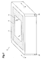
- an optical transmitting and receiving device 1 includes an enclosure 2 formed of, for example, a plastic material, in a rectangular-parallelepiped cup shape opened forward.
- a main body portion 4 which incorporates an LD (light emitting element) 9 that emits light forward and a PD (photodetecting element) that receives light irradiated from the front, and around the main body portion 4 in the enclosure 2, filled is, for example, an insulating-coated, light shielding resin 3 made of a silicone resin containing a carbon filler.
- This optical transmitting and receiving device 1 is used as, for example, a blood flow sensor that detects a blood flow in a body tissue and measures a blood flow volume, a blood flow velocity, a pulse, and the like by means of scattered light scattered by irradiating light on the body tissue.
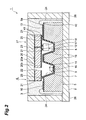
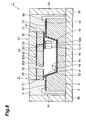
- the main body portion 4 has a base substrate 5 at a bottom-surface side in the enclosure 2.
- This base substrate 5 is formed of, for example, silicon being a semiconductor material, in a rectangular plate shape with a width of 2.8mm, a length of 6.0mm, and a thickness of 1.0mm, and in a front surface 5a of the base substrate 5, formed is a recess-like first cavity (first recess) 7 and second cavity (second recess) 8.
- the LD 9 is disposed in the first cavity 7, and is electrically connected with an LD anode 10 and an LD cathode 11 to be described later.
- the PD 12 is disposed in the second cavity 8, and is electrically connected with a PD anode 13 and a PD cathode 14 to be described later.
- the cavity 7, 8 is formed by, for example, applying wet etching to a silicon substrate to be the base substrate 5.
- the cavity 7, 8 is formed by providing, on the surface of a silicon substrate to be the base substrate 5, a mask formed of SiN or the like to demarcate the shape of the cavity 7, 8 and making an etchant act on an opening of this mask. After etching, the SiN mask is removed, and an insulating film 40 with a thickness of 1.5 ⁇ m and made of, for example, SiO 2 is then formed on, at least, the surface of the cavity and the surface of the substrate by thermal oxidation.
- the LD 9 uses, for example, a VCSEL (vertical-cavity surface-emitting laser) made of a compound semiconductor material with a thickness of 0.2mm, and this emits light having a wavelength of 850nm.
- a VCSEL vertical-cavity surface-emitting laser
- an LD terminal electrode 15 is provided at the front end face
- an LD terminal electrode 16 is provided at the rear end face.
- the PD 12 uses, for example, a Si-PD or GaAs-PD made of a semiconductor material with a thickness of 0.3mm.
- a PD terminal electrode 17 and a PD terminal electrode 18 are provided at the front end face.
- the material of the PD 12 is selected according to the wavelength of light to be emitted by the LD 9. For example, when the wavelength of light to be emitted by the LD 9 is 780nm, Si or GaAs is used as the material of the PD 12, and when the wavelength of light to be emitted by the LD 9 is 1.31 ⁇ m, InGaAs is used as the material of the PD 12.
- a base substrate wiring portion (wiring) 19 with a predetermined pattern On the insulating film 40 on the front surface 5a of the base substrate 5 and the inner surface of the cavity 7, 8, formed by, for example, an A1 film, a Ti-Pt-Au laminated film, or a Cr-Pt-Au laminated film is a base substrate wiring portion (wiring) 19 with a predetermined pattern.
- This base substrate wiring portion 19 has an LD anode 10 and an LD cathode 11 on the first cavity 7 side and has a PD anode 13 and a PD cathode 14 on the second cavity 8 side.
- the LD anode 10, LD cathode 11, PD anode 13, and PD cathode 14 are, as shown in Fig. 1 and Fig.
- the LD terminal electrode 16 of the LD 9 is electrically connected via, for example, a solder, a conductive resin, or the like.
- a light shielding member 20 formed of, for example, a silicon substrate coated with an insulating film 41 made of SiO 2 in a rectangular plate shape with a thickness of 0.15mm to 0.30mm, and this is fixed by bump bonding 21.
- the material for the bump bonding 21 include Au, Ni, Cu, AuSn, and SnAg-based solders.
- a light shielding portion may be formed by applying or filling a light shielding material.
- the light shielding member 20 formed is an opening (first light passing hole) 22 provided at a position corresponding to the first cavity 7 and a pinhole (second light passing hole) 23 provided at a position corresponding to the second cavity 8.
- the opening 22 guides light emitted from the LD 9 to the outside.
- the pinhole 23 guides scattered light from the outside to the PD 12 and also prevents ambient light and unnecessary light from the outside from entering the PD 12.
- the opening 22 and the pinhole 23 are formed by, for example, applying dry etching to a silicon substrate to be the light shielding member 20, and the pinhole 23 has a high aspect ratio.
- the pinhole 23 is formed at a position corresponding to a photodetecting surface of the PD 12, and the diameter thereof is provided as, for example, 30 ⁇ m to 90 ⁇ m. This is because noise due to ambient light and unnecessary light from the outside to be sensed by the PD 12 is increased when the diameter of the pinhole 23 is larger than 90 ⁇ m, while when the diameter of the pinhole 23 is smaller than 30 ⁇ m, light to be received by the PD 12 is reduced, so that an output from the PD 12 is lowered.
- a light shielding member wiring portion 25 is formed with a predetermined pattern, and this is electrically connected with the base substrate wiring portion 19 by bump bonding 21.
- the PD terminal electrode 17, 18 of the PD 12 is electrically connected (so-called, flip-chip bonding) by bump bonding 21.
- the PD 12 is electrically connected with each of the PD anode 13 and PD cathode 14.
- a light transmitting member 27 formed of, for example, alkali-containing borosilicate glass in a rectangular plate shape with a thickness of 0.3mm so that light emitted from the LD 9 and scattered light from the outside are transmitted therethrough, and this is fixed by a resin.
- This light transmitting member 27 enhances mechanical strength of the light shielding member 20 and also seals the first cavity 7 and the second cavity 8 of the base substrate 5 into a package.
- the coefficient of thermal expansion of the light transmitting member 27 and the coefficient of thermal expansion of the light shielding member 20 are set almost equal.
- the light shielding member 20 and the light transmitting member 27 may be fixed by anodic bonding. When anodic bonding is performed, the insulating film 41 is no longer necessary on the light transmitting member 27 side.
- the LD terminal electrode 15 of the LD 9 is electrically connected, via a wire 28, to the base substrate wiring portion 19 formed on the insulating film 40 on the front surface 5a of the base substrate 5.
- a wire storing portion 29 is formed in the light shielding member 20 laminated on and fixed to the front surface 5a side of the base substrate 5. Since these make it no longer necessary to provide a space to store the wire 28 in the first cavity 7, it becomes possible to downsize the first cavity 7. Accordingly, it becomes possible not only to downsize the base substrate 5 but also to downsize the optical transmitting and receiving device 1.
- the wire storing portion 29 to store the wire 28 is a through-hole, and this through-hole and the opening 22 are continuously formed. Adopting such a construction allows simply forming the wire storing portion 29 along with the opening 22.
- a part of the scattered light thus scattered advances in a direction opposite the forward direction of the light emitted from the LD 9, is transmitted through the light transmitting member 27, passes through the pinhole 23 formed in the light shielding member 20, and reaches the PD 12 disposed in the second cavity 8 of the base substrate 5. Then, a voltage signal in response to the reached light is obtained from the PD anode 13 and the PD cathode 14 of the base substrate wiring portion 19.
- the scattered light contains an interference component between scattered light from a stationary body tissue and scattered light that has received a Doppler shift from red blood cells moving in the capillaries of a body tissue, a frequency analysis of the voltage signal obtained by the PD 12 enables blood flow measurements etc.
- the optical transmitting and receiving device 1 according to a second embodiment differs in the shape of the wire storing portion 29 from the optical transmitting and receiving device 1 according to the first embodiment. More specifically, in the optical transmitting and receiving device 1 according to the second embodiment, as shown in Fig. 5 , the wire storing portion 29 is provided as a recess formed on the rear surface 20b of the light shielding member 20, and is formed continuously with the opening 22.
- optical transmitting and receiving device 1 according to the second embodiment constructed as such also provides the same operations and effects as those of the optical transmitting and receiving device 1 according to the first embodiment.
- the optical transmitting and receiving device 1 according to a third embodiment differs in the construction of the PD 12 from the optical transmitting and receiving device 1 according to the first embodiment. More specifically, in the optical transmitting and receiving device 1 according to the third embodiment, as shown in Fig. 6 and Fig. 7 , the PD terminal electrode 17 is provided at the front end face of the PD 12 and the PD terminal electrode 18 is provided at the rear end face of the PD 12. And, the PD terminal electrode 17 is electrically connected, via a wire 31, with the base substrate wiring portion 19 formed on the insulating film 40 on the front surface 5a of the base substrate 5, and the PD terminal electrode 18 is electrically connected with the base substrate wiring portion 19 formed on the insulating film 40 on the bottom surface of the second cavity 8.
- the wire storing portion 32 On the rear surface 20b of the light shielding member 20, formed as a recess is a wire storing portion 32 to store the wire 31, and the wire storing portion 32 is formed continuously with the pinhole 23. Also, in consideration of ambient light and unnecessary light that enter the PD 12, the length of the pinhole 23 is provided as 0.1mm or more.
- optical transmitting and receiving device 1 according to the third embodiment constructed as such also provides the same operations and effects as those of the optical transmitting and receiving device 1 according to the first embodiment.
- the optical transmitting and receiving device 1 according to the fourth embodiment differs in the shape of the base substrate 5 from the optical transmitting and receiving device 1 according to the first embodiment. More specifically, in the optical transmitting and receiving device 1 according to the fourth embodiment, as shown in Fig. 8 and Fig. 9 , a cavity (recess) 33 in which the LD 9 and the PD 12 are disposed is formed in the front surface 5a of the base substrate 5. Between the light shielding member 20 and the PD 12, a light shielding portion 34 made of a light shielding resin is provided so as to surround a photodetecting surface 12a of the PD 12. This prevents ambient light and unnecessary light from entering the PD 12 due to light emission or the like of the LD 9.
- optical transmitting and receiving device 1 according to the fourth embodiment constructed as such also provides the same operations and effects as those of the optical transmitting and receiving device 1 according to the first embodiment.
- an optical transmitting and receiving device may be constructed such that a wire electrically connected with the LD terminal electrode of an LD is stored in a wire storing portion which is a recess formed in the rear surface of a light shielding member and a wire electrically connected with the PD terminal electrode of a PD is stored in a wire storing portion which is a recess formed in the rear surface of a light shielding member.
- an optical transmitting and receiving device may be constructed such that an LD formed at the front end face with an anode-side LD terminal electrode and a cathode-side LD terminal electrode is electrically connected by flip-chip bonding with a light shielding member wiring portion formed on an insulating film on the rear surface of a light shielding member and a wire electrically connected with the PD terminal electrode of a PD is stored in a wire storing portion which is a recess formed in the rear surface of the light shielding member.
- the through-hole may be formed discontinuously with the opening (that is, independently of the opening).
- the recess may be formed discontinuously with the opening or pinhole (that is, independently of the opening or pinhole).
Abstract
An optical transmitting and receiving device 1 includes a main body portion 4 and has a base substrate 5 at a bottom-surface side of this main body 4. In a front surface 5a of this base substrate 5, formed is a recess-like first cavity 7 and second cavity 8, and an LD 9 is disposed in the first cavity 7, and a PD 12 is disposed in the second cavity 8. An LD terminal electrode 15 of the LD 9 is electrically connected, via a wire 28, to a base substrate wiring portion 19 formed on an insulating film 40 on the front surface 5a. Moreover, in a light shielding member 20 laminated on and fixed to the front surface 5a side of the base substrate 5, formed is a wire storing portion 29 to store the wire 28. Since these make it no longer necessary to provide a space to store the wire 28 in the first cavity 7, it becomes possible to downsize the first cavity 7. Accordingly, it becomes possible not only to downsize the base substrate 5 but also to downsize the optical transmitting and receiving device 1.
Description
- The present invention relates to an optical transmitting and receiving device which is used mainly as a blood flow sensor for measuring a blood flow volume and the like.
- As a conventional optical transmitting and receiving device, known is a blood flowmeter including a semiconductor substrate formed in its surface with recesses in which a light emitting element and a photodetecting element are disposed, respectively, and a cover substrate disposed on the surface of the semiconductor substrate and formed with a light shielding film (see
Patent Document 1, for example). In this blood flowmeter, one terminal electrode of the light emitting element is electrically connected with an electrode formed on an inner surface of the recess via a wire.
Patent Document 1: Japanese Published Unexamined Patent Application No.2004-229920 - However, such an optical transmitting and receiving device as described above has the following problem. That is, since one terminal electrode of the light emitting element is electrically connected with an electrode formed on an inner surface of the recess via a wire, it becomes necessary to provide a space to store the wire in the recess, so that the recess is increased in size by that space. Therefore, this hinders downsizing of the semiconductor substrate, and moreover, hinders downsizing of the optical transmitting and receiving device.
- Hence, the present invention has been made in view of such circumstances, and it is an object to provide an optical transmitting and receiving device that can be downsized.
- In order to attain the object described above, an optical transmitting and receiving device according to the present invention includes: a light emitting element for emitting light forward; a photodetecting element for receiving light irradiated from the front; a base substrate formed at a front surface thereof with a first recess in which the light emitting element is disposed and a second recess in which the photodetecting element is disposed; a light shielding member disposed at a front-surface side of the base substrate and formed with a first light passing hole through which light emitted by the light emitting element passes and a second light passing hole through which light to be received by the photodetecting element passes; and a light transmitting member which is disposed at a front-surface side of the light shielding member and through which light emitted by the light emitting element and light to be received by the photodetecting element are transmitted, wherein at least one of terminal electrodes of the light emitting element and terminal electrodes of the photodetecting element is electrically connected, via a wire, with a wiring formed on the front surface of the base substrate, and in the light shielding member, a wire storing portion to store the wire is formed.
- Moreover, an optical transmitting and receiving device includes: a light emitting element for emitting light forward; a photodetecting element for receiving light irradiated from the front; a base substrate formed at a front surface thereof with a recess in which the light emitting element and the photodetecting element are disposed; a light shielding member disposed at a front-surface side of the base substrate and formed with a first light passing hole through which light emitted by the light emitting element passes and a second light passing hole through which light to be received by the photodetecting element passes; and a light transmitting member which is disposed at a front-surface side of the light shielding member and through which light emitted by the light emitting element and light to be received by the photodetecting element are transmitted, wherein at least one of terminal electrodes of the light emitting element and terminal electrodes of the photodetecting element is electrically connected, via a wire, with a wiring formed on the front surface of the base substrate, and in the light shielding member, a wire storing portion to store the wire is formed.
- In these optical transmitting and receiving devices, at least one of terminal electrodes of the light emitting element and terminal electrodes of the photodetecting element is electrically connected, via a wire, with a wiring formed on the front surface of the base substrate, and in the light shielding member disposed at a front-surface side of the base substrate, a wire storing portion to store the wire is formed. Since this makes it no longer necessary to provide a space to store the wire in the recess, it becomes possible to downsize the recess. Accordingly, it becomes possible not only to downsize the base substrate but also to downsize the optical transmitting and receiving device.
- In the optical transmitting and receiving device according to the present invention, it is preferable that the wire storing portion to store the wire electrically connected with at least one of the terminal electrodes of the light emitting element is a recess or a through-hole. In this case, the wire storing portion can be simply formed.
- In the optical transmitting and receiving device according to the present invention, it is preferable that the wire storing portion to store the wire electrically connected with at least one of the terminal electrodes of the light emitting element is a through-hole, and this through-hole and the first light passing hole are continuously formed. In this case, the wire storing portion can be further simply formed.
- In the optical transmitting and receiving device according to the present invention, it is preferable that the wire storing portion to store the wire electrically connected with at least one of the terminal electrodes of the photodetecting element is a recess. In this case, the wire storing portion can be simply formed, and light irradiated from the front can be prevented from being received by the wire storing portion via the wire storing portion.
- According to the present invention, it becomes possible to downsize an optical transmitting and receiving device.
-
- [
Fig. 1 ] A schematic perspective view of an optical transmitting and receiving device according to a first embodiment. - [
Fig. 2 ] A schematic end view along a line II-II shown inFig. 1 . - [
Fig. 3 ] A schematic exploded perspective view of a main body portion of the optical transmitting and receiving device shown inFig. 1 . - [
Fig. 4 ] A schematic end view along a line IV-IV shown inFig. 3 . - [
Fig. 5 ] A schematic end view, of a main body portion of an optical transmitting and receiving device according to a second embodiment, corresponding toFig. 4 . - [
Fig. 6 ] A schematic end view, of an optical transmitting and receiving device according to a third embodiment, corresponding toFig. 2 . - [
Fig. 7 ] A schematic end view along a line VII-VII shown inFig. 6 . - [
Fig. 8 ] A schematic end view, of an optical transmitting and receiving device according to a fourth embodiment, corresponding toFig. 2 . - [
Fig. 9 ] A schematic end view, of a main body portion of the optical transmitting and receiving device according to the fourth embodiment, corresponding toFig. 4 . - 1... optical transmitting and receiving device, 5 ... base substrate, 5a ... front surface, 7 ... first cavity (first recess), 8 ... second cavity (second recess), 9 ... LD (light emitting element), 12 ... PD (photodetecting element), 15, 16 ... LD terminal electrode, 17, 18 ... PD terminal electrode, 19 ... base substrate wiring portion (wiring), 20 ... light shielding member, 22 ... opening (first light passing hole), 23 ... pinhole (second light passing hole), 27 ... light transmitting member, 28, 31 ... wire, 29, 32 ... wire storing portion , 33 ... cavity (recess).
- Hereinafter, preferred embodiments of the present invention will be described in detail with reference to the accompanying drawings. Also, the same or equivalent parts are denoted with the same reference numerals in the respective figures, and overlapping description will thus be omitted.
- As shown in
Fig. 1 andFig. 2 , an optical transmitting and receivingdevice 1 according to a first embodiment includes anenclosure 2 formed of, for example, a plastic material, in a rectangular-parallelepiped cup shape opened forward. In theenclosure 2, disposed is amain body portion 4 which incorporates an LD (light emitting element) 9 that emits light forward and a PD (photodetecting element) that receives light irradiated from the front, and around themain body portion 4 in theenclosure 2, filled is, for example, an insulating-coated,light shielding resin 3 made of a silicone resin containing a carbon filler. This optical transmitting and receivingdevice 1 is used as, for example, a blood flow sensor that detects a blood flow in a body tissue and measures a blood flow volume, a blood flow velocity, a pulse, and the like by means of scattered light scattered by irradiating light on the body tissue. - As shown in
Fig. 2 andFig. 3 , themain body portion 4 has abase substrate 5 at a bottom-surface side in theenclosure 2. Thisbase substrate 5 is formed of, for example, silicon being a semiconductor material, in a rectangular plate shape with a width of 2.8mm, a length of 6.0mm, and a thickness of 1.0mm, and in afront surface 5a of thebase substrate 5, formed is a recess-like first cavity (first recess) 7 and second cavity (second recess) 8. TheLD 9 is disposed in thefirst cavity 7, and is electrically connected with anLD anode 10 and anLD cathode 11 to be described later. Moreover, thePD 12 is disposed in thesecond cavity 8, and is electrically connected with aPD anode 13 and aPD cathode 14 to be described later. - Also, the
cavity base substrate 5. Concretely, thecavity base substrate 5, a mask formed of SiN or the like to demarcate the shape of thecavity insulating film 40 with a thickness of 1.5µm and made of, for example, SiO2 is then formed on, at least, the surface of the cavity and the surface of the substrate by thermal oxidation. - The LD 9 uses, for example, a VCSEL (vertical-cavity surface-emitting laser) made of a compound semiconductor material with a thickness of 0.2mm, and this emits light having a wavelength of 850nm. In this
LD 9, anLD terminal electrode 15 is provided at the front end face, and anLD terminal electrode 16 is provided at the rear end face. Moreover, thePD 12 uses, for example, a Si-PD or GaAs-PD made of a semiconductor material with a thickness of 0.3mm. In thisLD 12, aPD terminal electrode 17 and aPD terminal electrode 18 are provided at the front end face. - Also, the material of the
PD 12 is selected according to the wavelength of light to be emitted by theLD 9. For example, when the wavelength of light to be emitted by theLD 9 is 780nm, Si or GaAs is used as the material of thePD 12, and when the wavelength of light to be emitted by theLD 9 is 1.31µm, InGaAs is used as the material of thePD 12. - On the
insulating film 40 on thefront surface 5a of thebase substrate 5 and the inner surface of thecavity substrate wiring portion 19 has anLD anode 10 and anLD cathode 11 on thefirst cavity 7 side and has aPD anode 13 and aPD cathode 14 on thesecond cavity 8 side. TheLD anode 10,LD cathode 11,PD anode 13, andPD cathode 14 are, as shown inFig. 1 andFig. 2 , electrically connected, viawires 24, withelectrodes 26 formed at four corners in the bottom of theenclosure 2, in a manner extracting the electrodes from the front surface to the rear surface thereof. And, to the basesubstrate wiring portion 19 formed on theinsulating film 40 on the bottom surface of thefirst cavity 7, theLD terminal electrode 16 of theLD 9 is electrically connected via, for example, a solder, a conductive resin, or the like. - Returning to
Fig. 2 andFig. 3 , on the insulatingfilm 40 on thefront surface 5a of thebase substrate 5, laminated is alight shielding member 20 formed of, for example, a silicon substrate coated with an insulatingfilm 41 made of SiO2 in a rectangular plate shape with a thickness of 0.15mm to 0.30mm, and this is fixed bybump bonding 21. Examples of the material for thebump bonding 21 include Au, Ni, Cu, AuSn, and SnAg-based solders. Here, it is preferable to pave a part between thefirst cavity 7 and thesecond cavity 8 with bump bonding 21 so that light emitted from theLD 9 does not reach thePD 12 through a gap between thebase substrate 5 and thelight shielding member 20. Alternatively, in this part, a light shielding portion may be formed by applying or filling a light shielding material. - In the
light shielding member 20, formed is an opening (first light passing hole) 22 provided at a position corresponding to thefirst cavity 7 and a pinhole (second light passing hole) 23 provided at a position corresponding to thesecond cavity 8. Theopening 22 guides light emitted from theLD 9 to the outside. Moreover, thepinhole 23 guides scattered light from the outside to thePD 12 and also prevents ambient light and unnecessary light from the outside from entering thePD 12. Also, theopening 22 and thepinhole 23 are formed by, for example, applying dry etching to a silicon substrate to be thelight shielding member 20, and thepinhole 23 has a high aspect ratio. - Also, the
pinhole 23 is formed at a position corresponding to a photodetecting surface of thePD 12, and the diameter thereof is provided as, for example, 30µm to 90µm. This is because noise due to ambient light and unnecessary light from the outside to be sensed by thePD 12 is increased when the diameter of thepinhole 23 is larger than 90µm, while when the diameter of thepinhole 23 is smaller than 30µm, light to be received by thePD 12 is reduced, so that an output from thePD 12 is lowered. - On the insulating
film 41 on arear surface 20b of thelight shielding member 20, a light shieldingmember wiring portion 25 is formed with a predetermined pattern, and this is electrically connected with the basesubstrate wiring portion 19 bybump bonding 21. At a part corresponding to thesecond cavity 8 in the light shieldingmember wiring portion 25, thePD terminal electrode PD 12 is electrically connected (so-called, flip-chip bonding) bybump bonding 21. Thereby, thePD 12 is electrically connected with each of thePD anode 13 andPD cathode 14. - Moreover, on the insulating
film 41 on afront surface 20a of thelight shielding member 20, laminated is alight transmitting member 27 formed of, for example, alkali-containing borosilicate glass in a rectangular plate shape with a thickness of 0.3mm so that light emitted from theLD 9 and scattered light from the outside are transmitted therethrough, and this is fixed by a resin. Thislight transmitting member 27 enhances mechanical strength of thelight shielding member 20 and also seals thefirst cavity 7 and thesecond cavity 8 of thebase substrate 5 into a package. Also, since thelight transmitting member 27 is fixed to thelight shielding member 20, the coefficient of thermal expansion of thelight transmitting member 27 and the coefficient of thermal expansion of thelight shielding member 20 are set almost equal. Alternatively, thelight shielding member 20 and thelight transmitting member 27 may be fixed by anodic bonding. When anodic bonding is performed, the insulatingfilm 41 is no longer necessary on thelight transmitting member 27 side. - Meanwhile, in the optical transmitting and receiving
device 1, as shown inFig. 4 , theLD terminal electrode 15 of theLD 9 is electrically connected, via awire 28, to the basesubstrate wiring portion 19 formed on the insulatingfilm 40 on thefront surface 5a of thebase substrate 5. Moreover, in thelight shielding member 20 laminated on and fixed to thefront surface 5a side of thebase substrate 5, formed is awire storing portion 29 to store thewire 28. Since these make it no longer necessary to provide a space to store thewire 28 in thefirst cavity 7, it becomes possible to downsize thefirst cavity 7. Accordingly, it becomes possible not only to downsize thebase substrate 5 but also to downsize the optical transmitting and receivingdevice 1. - Further, in the
light shielding member 20, thewire storing portion 29 to store thewire 28 is a through-hole, and this through-hole and theopening 22 are continuously formed. Adopting such a construction allows simply forming thewire storing portion 29 along with theopening 22. - When, for example, information concerning a fluid substance in a body such as a blood flow volume and the like in a body tissue is measured by use of the optical transmitting and receiving
device 1 constructed as in the above, voltage is supplied to theLD anode 10 and theLD cathode 11 of the basesubstrate wiring portion 19 so as to emit light fromLD 9 disposed in thefirst cavity 7 of thebase substrate 5. This light passes through theopening 22 formed in thelight shielding member 20, is transmitted through thelight transmitting member 27 to be emitted to the outside, and then advances in the body tissue to be, for example, scattered by blood flow components. A part of the scattered light thus scattered advances in a direction opposite the forward direction of the light emitted from theLD 9, is transmitted through thelight transmitting member 27, passes through thepinhole 23 formed in thelight shielding member 20, and reaches thePD 12 disposed in thesecond cavity 8 of thebase substrate 5. Then, a voltage signal in response to the reached light is obtained from thePD anode 13 and thePD cathode 14 of the basesubstrate wiring portion 19. Here, since the scattered light contains an interference component between scattered light from a stationary body tissue and scattered light that has received a Doppler shift from red blood cells moving in the capillaries of a body tissue, a frequency analysis of the voltage signal obtained by thePD 12 enables blood flow measurements etc. - The optical transmitting and receiving
device 1 according to a second embodiment differs in the shape of thewire storing portion 29 from the optical transmitting and receivingdevice 1 according to the first embodiment. More specifically, in the optical transmitting and receivingdevice 1 according to the second embodiment, as shown inFig. 5 , thewire storing portion 29 is provided as a recess formed on therear surface 20b of thelight shielding member 20, and is formed continuously with theopening 22. - The optical transmitting and receiving
device 1 according to the second embodiment constructed as such also provides the same operations and effects as those of the optical transmitting and receivingdevice 1 according to the first embodiment. - The optical transmitting and receiving
device 1 according to a third embodiment differs in the construction of thePD 12 from the optical transmitting and receivingdevice 1 according to the first embodiment. More specifically, in the optical transmitting and receivingdevice 1 according to the third embodiment, as shown inFig. 6 andFig. 7 , thePD terminal electrode 17 is provided at the front end face of thePD 12 and thePD terminal electrode 18 is provided at the rear end face of thePD 12. And, thePD terminal electrode 17 is electrically connected, via awire 31, with the basesubstrate wiring portion 19 formed on the insulatingfilm 40 on thefront surface 5a of thebase substrate 5, and thePD terminal electrode 18 is electrically connected with the basesubstrate wiring portion 19 formed on the insulatingfilm 40 on the bottom surface of thesecond cavity 8. On therear surface 20b of thelight shielding member 20, formed as a recess is awire storing portion 32 to store thewire 31, and thewire storing portion 32 is formed continuously with thepinhole 23. Also, in consideration of ambient light and unnecessary light that enter thePD 12, the length of thepinhole 23 is provided as 0.1mm or more. - The optical transmitting and receiving
device 1 according to the third embodiment constructed as such also provides the same operations and effects as those of the optical transmitting and receivingdevice 1 according to the first embodiment. - The optical transmitting and receiving
device 1 according to the fourth embodiment differs in the shape of thebase substrate 5 from the optical transmitting and receivingdevice 1 according to the first embodiment. More specifically, in the optical transmitting and receivingdevice 1 according to the fourth embodiment, as shown inFig. 8 andFig. 9 , a cavity (recess) 33 in which theLD 9 and thePD 12 are disposed is formed in thefront surface 5a of thebase substrate 5. Between thelight shielding member 20 and thePD 12, alight shielding portion 34 made of a light shielding resin is provided so as to surround aphotodetecting surface 12a of thePD 12. This prevents ambient light and unnecessary light from entering thePD 12 due to light emission or the like of theLD 9. - The optical transmitting and receiving
device 1 according to the fourth embodiment constructed as such also provides the same operations and effects as those of the optical transmitting and receivingdevice 1 according to the first embodiment. - In the above, although preferred embodiments of the present invention have been described, the present invention is not limited to the abovementioned embodiments.
- For example, an optical transmitting and receiving device may be constructed such that a wire electrically connected with the LD terminal electrode of an LD is stored in a wire storing portion which is a recess formed in the rear surface of a light shielding member and a wire electrically connected with the PD terminal electrode of a PD is stored in a wire storing portion which is a recess formed in the rear surface of a light shielding member. Alternatively, an optical transmitting and receiving device may be constructed such that an LD formed at the front end face with an anode-side LD terminal electrode and a cathode-side LD terminal electrode is electrically connected by flip-chip bonding with a light shielding member wiring portion formed on an insulating film on the rear surface of a light shielding member and a wire electrically connected with the PD terminal electrode of a PD is stored in a wire storing portion which is a recess formed in the rear surface of the light shielding member.
- Further, when the wire storing portion is a through-hole, the through-hole may be formed discontinuously with the opening (that is, independently of the opening). Moreover, when the wire storing portion is a recess, the recess may be formed discontinuously with the opening or pinhole (that is, independently of the opening or pinhole).
- According to the present invention, it becomes possible to downsize an optical transmitting and receiving device.
Claims (5)
- An optical transmitting and receiving device comprising:a light emitting element for emitting light forward;a photodetecting element for receiving light irradiated from the front;a base substrate formed at a front surface thereof with a first recess in which the light emitting element is disposed and a second recess in which the photodetecting element is disposed;a light shielding member disposed at a front-surface side of the base substrate and formed with a first light passing hole through which light emitted by the light emitting element passes and a second light passing hole through which light to be received by the photodetecting element passes; anda light transmitting member which is disposed at a front-surface side of the light shielding member and through which light emitted by the light emitting element and light to be received by the photodetecting element are transmitted, whereinat least one of terminal electrodes of the light emitting element and terminal electrodes of the photodetecting element is electrically connected, via a wire, with a wiring formed on the front surface of the base substrate, andin the light shielding member, a wire storing portion to store the wire is formed.
- An optical transmitting and receiving device comprising:a light emitting element for emitting light forward;a photodetecting element for receiving light irradiated from the front;a base substrate formed at a front surface thereof with a recess in which the light emitting element and the photodetecting element are disposed;a light shielding member disposed at a front-surface side of the base substrate and formed with a first light passing hole through which light emitted by the light emitting element passes and a second light passing hole through which light to be received by the photodetecting element passes; anda light transmitting member which is disposed at a front-surface side of the light shielding member and through which light emitted by the light emitting element and light to be received by the photodetecting element are transmitted, whereinat least one of terminal electrodes of the light emitting element and terminal electrodes of the photodetecting element is electrically connected, via a wire, with a wiring formed on the front surface of the base substrate, andin the light shielding member, a wire storing portion to store the wire is formed.
- The optical transmitting and receiving device according to Claim 1 or 2, wherein the wire storing portion to store the wire electrically connected with at least one of the terminal electrodes of the light emitting element is a recess or a through-hole.
- The optical transmitting and receiving device according to Claim 1 or 2, wherein the wire storing portion to store the wire electrically connected with at least one of the terminal electrodes of the light emitting element is a through-hole, and this through-hole and the first light passing hole are continuously formed.
- The optical transmitting and receiving device according to Claim 1 or 2, wherein the wire storing portion to store the wire electrically connected with at least one of the terminal electrodes of the photodetecting element is a recess.
Applications Claiming Priority (2)
| Application Number | Priority Date | Filing Date | Title |
|---|---|---|---|
| JP2006047249A JP4708214B2 (en) | 2006-02-23 | 2006-02-23 | Optical transceiver device |
| PCT/JP2007/052696 WO2007097240A1 (en) | 2006-02-23 | 2007-02-15 | Optical transmission/reception device |
Publications (2)
| Publication Number | Publication Date |
|---|---|
| EP1993148A1 true EP1993148A1 (en) | 2008-11-19 |
| EP1993148A4 EP1993148A4 (en) | 2010-12-22 |
Family
ID=38437278
Family Applications (1)
| Application Number | Title | Priority Date | Filing Date |
|---|---|---|---|
| EP07714226A Withdrawn EP1993148A4 (en) | 2006-02-23 | 2007-02-15 | Optical transmission/reception device |
Country Status (7)
| Country | Link |
|---|---|
| US (1) | US20090202251A1 (en) |
| EP (1) | EP1993148A4 (en) |
| JP (1) | JP4708214B2 (en) |
| KR (1) | KR20080100332A (en) |
| CN (1) | CN101371373B (en) |
| TW (1) | TWI398969B (en) |
| WO (1) | WO2007097240A1 (en) |
Cited By (4)
| Publication number | Priority date | Publication date | Assignee | Title |
|---|---|---|---|---|
| EP2745772A4 (en) * | 2011-08-19 | 2015-09-16 | Murata Manufacturing Co | Living organism sensor |
| KR20180072766A (en) * | 2016-01-25 | 2018-06-29 | 쿄세라 코포레이션 | Package for measuring sensor and measuring sensor |
| EP3395242A4 (en) * | 2015-12-22 | 2019-09-04 | KYOCERA Corporation | Measuring sensor package and measuring sensor |
| EP3745090A1 (en) * | 2019-05-27 | 2020-12-02 | Dr. Johannes Heidenhain GmbH | Light source and method for producing the same and position measuring device comprising a light source |
Families Citing this family (22)
| Publication number | Priority date | Publication date | Assignee | Title |
|---|---|---|---|---|
| JP4943739B2 (en) * | 2006-05-18 | 2012-05-30 | 浜松ホトニクス株式会社 | Optical transceiver device |
| JP5031894B2 (en) * | 2008-05-12 | 2012-09-26 | パイオニア株式会社 | Self-luminous sensor device |
| KR101064072B1 (en) | 2009-02-24 | 2011-09-08 | 엘지이노텍 주식회사 | Light emitting device package |
| CN102375185B (en) * | 2010-08-20 | 2013-11-13 | 国碁电子(中山)有限公司 | Optical transceiver and manufacturing method thereof |
| JP5709165B2 (en) * | 2011-03-10 | 2015-04-30 | セイコーインスツル株式会社 | Optical device |
| EP2745771B1 (en) * | 2011-08-19 | 2020-11-25 | Murata Manufacturing Co., Ltd. | Living organism sensor |
| US8675706B2 (en) * | 2011-12-24 | 2014-03-18 | Princeton Optronics Inc. | Optical illuminator |
| US9981844B2 (en) | 2012-03-08 | 2018-05-29 | Infineon Technologies Ag | Method of manufacturing semiconductor device with glass pieces |
| JP6030656B2 (en) * | 2012-08-30 | 2016-11-24 | 京セラ株式会社 | Light emitting / receiving element and sensor device using the same |
| JP6229338B2 (en) * | 2013-07-12 | 2017-11-15 | セイコーエプソン株式会社 | Photodetection unit and biological information detection apparatus |
| JP6453362B2 (en) * | 2014-12-11 | 2019-01-16 | 愛知時計電機株式会社 | Blood flow sensor |
| WO2017175504A1 (en) * | 2016-04-04 | 2017-10-12 | 京セラ株式会社 | Measurement sensor package and measurement sensor |
| JP6631423B2 (en) * | 2016-07-04 | 2020-01-15 | オムロン株式会社 | Biological information detecting device and chair provided with biological information detecting device |
| US20180017741A1 (en) * | 2016-07-15 | 2018-01-18 | Advanced Semiconductor Engineering, Inc. | Semiconductor package device and method of manufacturing the same |
| JP6718339B2 (en) * | 2016-09-06 | 2020-07-08 | 京セラ株式会社 | Measurement sensor package and measurement sensor |
| JP6891441B2 (en) * | 2016-10-12 | 2021-06-18 | セイコーエプソン株式会社 | Detection device and measuring device |
| WO2018153464A1 (en) | 2017-02-23 | 2018-08-30 | Osram Opto Semiconductors Gmbh | Sensor element |
| JP6735463B2 (en) * | 2017-03-24 | 2020-08-05 | 愛知時計電機株式会社 | Measuring device |
| US11255770B2 (en) * | 2018-01-30 | 2022-02-22 | Kyocera Corporation | Measurement apparatus |
| EP4357790A1 (en) * | 2018-04-24 | 2024-04-24 | Sony Group Corporation | Scattered light signal measuring device, and information processing device |
| EP3876257A4 (en) * | 2018-10-30 | 2022-08-17 | Kyocera Corporation | Optical sensor device |
| CN113015485A (en) * | 2018-11-12 | 2021-06-22 | 索尼集团公司 | Biological information measuring device |
Citations (5)
| Publication number | Priority date | Publication date | Assignee | Title |
|---|---|---|---|---|
| US5998862A (en) * | 1993-03-26 | 1999-12-07 | Sony Corporation | Air-packed CCD images package and a mold for manufacturing thereof |
| US6646290B1 (en) * | 2002-08-23 | 2003-11-11 | Amkor Technology, Inc. | Optical structure having an optical diode and a sensor in separate apertures inside double insulating layers |
| JP2004022802A (en) * | 2002-06-17 | 2004-01-22 | Korai Kagi Kofun Yugenkoshi | Heat dissipation structure used for package of semiconductor light emitting device and its manufacturing method |
| JP2004229920A (en) * | 2003-01-30 | 2004-08-19 | Nippon Telegr & Teleph Corp <Ntt> | Sensor part of rheometer and rheometer |
| US20040256687A1 (en) * | 2003-02-07 | 2004-12-23 | Seiko Epson Corporation | Optical module, method of manufacturing the same, and electronic instrument |
Family Cites Families (4)
| Publication number | Priority date | Publication date | Assignee | Title |
|---|---|---|---|---|
| EP0489177A4 (en) * | 1990-06-26 | 1993-06-09 | Seiko Epson Corporation | Semiconductor device and method of manufacturing the same |
| JP2002117702A (en) * | 2000-10-11 | 2002-04-19 | Toyoda Gosei Co Ltd | Light source device |
| US6574254B1 (en) * | 2002-02-08 | 2003-06-03 | Harvatek Corp. | Laser diode package with heat sinking substrate |
| JP2006013174A (en) * | 2004-06-25 | 2006-01-12 | Kyocera Corp | Optical semiconductor apparatus |
-
2006
- 2006-02-23 JP JP2006047249A patent/JP4708214B2/en active Active
-
2007
- 2007-02-15 KR KR1020087011109A patent/KR20080100332A/en not_active Application Discontinuation
- 2007-02-15 EP EP07714226A patent/EP1993148A4/en not_active Withdrawn
- 2007-02-15 WO PCT/JP2007/052696 patent/WO2007097240A1/en active Application Filing
- 2007-02-15 CN CN2007800030575A patent/CN101371373B/en active Active
- 2007-02-15 US US12/280,116 patent/US20090202251A1/en not_active Abandoned
- 2007-02-16 TW TW096105954A patent/TWI398969B/en active
Patent Citations (5)
| Publication number | Priority date | Publication date | Assignee | Title |
|---|---|---|---|---|
| US5998862A (en) * | 1993-03-26 | 1999-12-07 | Sony Corporation | Air-packed CCD images package and a mold for manufacturing thereof |
| JP2004022802A (en) * | 2002-06-17 | 2004-01-22 | Korai Kagi Kofun Yugenkoshi | Heat dissipation structure used for package of semiconductor light emitting device and its manufacturing method |
| US6646290B1 (en) * | 2002-08-23 | 2003-11-11 | Amkor Technology, Inc. | Optical structure having an optical diode and a sensor in separate apertures inside double insulating layers |
| JP2004229920A (en) * | 2003-01-30 | 2004-08-19 | Nippon Telegr & Teleph Corp <Ntt> | Sensor part of rheometer and rheometer |
| US20040256687A1 (en) * | 2003-02-07 | 2004-12-23 | Seiko Epson Corporation | Optical module, method of manufacturing the same, and electronic instrument |
Non-Patent Citations (1)
| Title |
|---|
| See also references of WO2007097240A1 * |
Cited By (11)
| Publication number | Priority date | Publication date | Assignee | Title |
|---|---|---|---|---|
| EP2745772A4 (en) * | 2011-08-19 | 2015-09-16 | Murata Manufacturing Co | Living organism sensor |
| EP3053519A1 (en) * | 2011-08-19 | 2016-08-10 | Murata Manufacturing Co., Ltd. | Biosensor |
| US9439569B2 (en) | 2011-08-19 | 2016-09-13 | Murata Manufacturing Co., Ltd. | Biosensor having light emitting and receiving elements to obtain a biological signal |
| US10111592B2 (en) | 2011-08-19 | 2018-10-30 | Murata Manufacturing Co., Ltd. | Biosensor |
| EP3395242A4 (en) * | 2015-12-22 | 2019-09-04 | KYOCERA Corporation | Measuring sensor package and measuring sensor |
| CN112168146A (en) * | 2015-12-22 | 2021-01-05 | 京瓷株式会社 | Measurement sensor package and measurement sensor |
| EP4026493A1 (en) * | 2015-12-22 | 2022-07-13 | Kyocera Corporation | Measuring sensor package and measurement sensor |
| KR20180072766A (en) * | 2016-01-25 | 2018-06-29 | 쿄세라 코포레이션 | Package for measuring sensor and measuring sensor |
| EP3410127A4 (en) * | 2016-01-25 | 2019-08-28 | Kyocera Corporation | Measurement sensor package and measurement sensor |
| US11717178B2 (en) | 2016-01-25 | 2023-08-08 | Kyocera Corporation | Measurement sensor package and measurement sensor |
| EP3745090A1 (en) * | 2019-05-27 | 2020-12-02 | Dr. Johannes Heidenhain GmbH | Light source and method for producing the same and position measuring device comprising a light source |
Also Published As
| Publication number | Publication date |
|---|---|
| EP1993148A4 (en) | 2010-12-22 |
| TWI398969B (en) | 2013-06-11 |
| WO2007097240A1 (en) | 2007-08-30 |
| US20090202251A1 (en) | 2009-08-13 |
| CN101371373A (en) | 2009-02-18 |
| KR20080100332A (en) | 2008-11-17 |
| JP4708214B2 (en) | 2011-06-22 |
| JP2007225923A (en) | 2007-09-06 |
| TW200802971A (en) | 2008-01-01 |
| CN101371373B (en) | 2011-04-27 |
Similar Documents
| Publication | Publication Date | Title |
|---|---|---|
| EP1993148A1 (en) | Optical transmission/reception device | |
| JP4586337B2 (en) | Semiconductor laser module and semiconductor laser device | |
| EP3566075B1 (en) | Vcsel narrow divergence proximity sensor | |
| JP5206944B2 (en) | Optical module and medical optical measurement system using the same | |
| US20120087136A1 (en) | Optical device | |
| JP2004272061A (en) | Optical communication module | |
| JP2011151080A (en) | Semiconductor laser device | |
| TWI392249B (en) | Optical transceiver device | |
| CN111919093B (en) | Flow velocity calculating device, flow velocity sensor device, flow device, and flow velocity calculating method | |
| US20210382319A1 (en) | Optical sensor device | |
| JP6999407B2 (en) | Optical sensor device | |
| JP7054609B2 (en) | Measurement sensor package and measurement sensor | |
| JP2018038546A (en) | Package for measurement sensor and measurement sensor | |
| KR20180012210A (en) | Optical semiconductor device | |
| JP4454233B2 (en) | Optical package and optical module using the same | |
| JP6462904B2 (en) | Measurement sensor package and measurement sensor | |
| CN217846619U (en) | Optical sensor | |
| JP2013030549A (en) | Light emitting module and member for chip component mounting | |
| JP2018196571A (en) | Package for measurement sensor and measurement sensor | |
| JP6753729B2 (en) | Measurement sensor package and measurement sensor | |
| JP2017192500A (en) | Measuring sensor package and measuring sensor | |
| US20210401300A1 (en) | Biological information measuring device | |
| JP2019058451A (en) | Optical sensor device | |
| JP2017192507A (en) | Measuring sensor package and measuring sensor | |
| JPS59152681A (en) | Light communication equipment |
Legal Events
| Date | Code | Title | Description |
|---|---|---|---|
| PUAI | Public reference made under article 153(3) epc to a published international application that has entered the european phase |
Free format text: ORIGINAL CODE: 0009012 |
|
| 17P | Request for examination filed |
Effective date: 20080821 |
|
| AK | Designated contracting states |
Kind code of ref document: A1 Designated state(s): DE FR GB |
|
| DAX | Request for extension of the european patent (deleted) | ||
| RBV | Designated contracting states (corrected) |
Designated state(s): DE FR GB |
|
| A4 | Supplementary search report drawn up and despatched |
Effective date: 20101124 |
|
| 17Q | First examination report despatched |
Effective date: 20101210 |
|
| STAA | Information on the status of an ep patent application or granted ep patent |
Free format text: STATUS: THE APPLICATION IS DEEMED TO BE WITHDRAWN |
|
| 18D | Application deemed to be withdrawn |
Effective date: 20110421 |