EP1990916A2 - Frequency modulator. - Google Patents
Frequency modulator. Download PDFInfo
- Publication number
- EP1990916A2 EP1990916A2 EP08155068A EP08155068A EP1990916A2 EP 1990916 A2 EP1990916 A2 EP 1990916A2 EP 08155068 A EP08155068 A EP 08155068A EP 08155068 A EP08155068 A EP 08155068A EP 1990916 A2 EP1990916 A2 EP 1990916A2
- Authority
- EP
- European Patent Office
- Prior art keywords
- signal
- digital
- oscillator
- frequency
- modulating
- Prior art date
- Legal status (The legal status is an assumption and is not a legal conclusion. Google has not performed a legal analysis and makes no representation as to the accuracy of the status listed.)
- Granted
Links
Images

Classifications
-
- H—ELECTRICITY
- H03—ELECTRONIC CIRCUITRY
- H03K—PULSE TECHNIQUE
- H03K7/00—Modulating pulses with a continuously-variable modulating signal
- H03K7/06—Frequency or rate modulation, i.e. PFM or PRM
-
- H—ELECTRICITY
- H03—ELECTRONIC CIRCUITRY
- H03B—GENERATION OF OSCILLATIONS, DIRECTLY OR BY FREQUENCY-CHANGING, BY CIRCUITS EMPLOYING ACTIVE ELEMENTS WHICH OPERATE IN A NON-SWITCHING MANNER; GENERATION OF NOISE BY SUCH CIRCUITS
- H03B23/00—Generation of oscillations periodically swept over a predetermined frequency range
-
- H—ELECTRICITY
- H04—ELECTRIC COMMUNICATION TECHNIQUE
- H04B—TRANSMISSION
- H04B15/00—Suppression or limitation of noise or interference
- H04B15/02—Reducing interference from electric apparatus by means located at or near the interfering apparatus
-
- H—ELECTRICITY
- H04—ELECTRIC COMMUNICATION TECHNIQUE
- H04B—TRANSMISSION
- H04B2215/00—Reducing interference at the transmission system level
- H04B2215/064—Reduction of clock or synthesizer reference frequency harmonics
- H04B2215/067—Reduction of clock or synthesizer reference frequency harmonics by modulation dispersion
Definitions
- the present invention relates to a frequency modulator, specifically a clock frequency modulator.
- EMI electromagnetic interferences
- a possibility to reduce electromagnetic interferences consists in the periodic or random modulation of a parameter of the signals which are applied to switching devices, such as the switching frequency.
- the parameter oscillates with small amplitudes around a nominal value, so that the power of the harmonics is distributed on the spectrum.
- the switching frequency thereof needs to be modulated so that the resulting action on the distribution spectrum allows the distribution of the energy of each harmonic of the switching frequency on a number of sideband harmonics which have the same energy though a smaller amplitude.
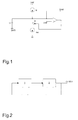
- a typical frequency modulator circuit adapted to generate a low-frequency triangular waveform is shown in Figure 1 .
- the circuit includes a capacitor C which is connected to ground GND and to a current generator Ic connected to a supply voltage Vdd and to a switch S which may be connected to another current generator Icc connected to ground GND.
- the capacitor is also connected to the non-inverting terminal of a hysteresis comparator Comp having the inverting terminal connected to a reference voltage Vref.
- the output voltage of the comparator Comp controls the closing or opening of the switch S for the generation of a triangular wave on the non-inverting terminal of the comparator Comp.
- the circuit topologies generally use the triangular waveform generated in this way as modulating reference voltage to control the oscillation frequency of the main oscillator.
- the triangular waveform is the modulating reference voltage which may be used to vary a circuit parameter of the oscillator so that the frequency of the oscillator is modulated by the modulating signal.
- a clock frequency modulator for an oscillator may be provided, characterised in that it includes digital means for the generation of a signal for modulating said clock frequency, said digital means including first means adapted to obtain from the signal generated by the oscillator a first pulse signal having a lower frequency than the clock frequency of the oscillator, a digital counter adapted to count the pulses of said first signal and to produce a digital signal and a digital to analog converter adapted to convert the digital signal in said signal for modulating the clock frequency of the oscillator.
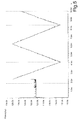
- Figure 2 shows a diagram of the frequency modulator according to the present invention.
- the diagram includes a digital-type triangular waveform generator 1, the output signal of which modulates an oscillator 2 adapted to provide the clock signal CLOCK.
- the triangular waveform generator 1 is shown in greater detail in Figure 3 .
- Said generator includes a first 3 and a second 4 frequency divider adapted to divide the frequency of the CLOCK signal by predetermined values which are different one from the other, a counter 5 supplied by the signals from the dividers 3 and 4 and a digital to analog converter (DAC) 6 having as an input the output signal from the counter 5 and adapted to generate the triangular waveform signal Vth.
- DAC digital to analog converter
- the digital counter 5 is preferably an N-bit counter capable of increasingly and decreasingly counting.
- the signal CLKb which has at least two logical levels, controls the counter 5 so that it increasingly or decreasingly counts while the signal CLKf is the counted signal; said signal is a pulse signal, which pulses are counted by the counter 5.
- the signal CLKb is generally a square wave signal and the counter 5 increasingly or decreasingly counts the pulses of the signal CLKf until the state of the signal CLKb changes; the counted digital word is issued in real time as an input to the DAC 6 which provides an output voltage value.
- the waveform of the modulating reference voltage signal Vth produced by the DAC 6 will be a triangular form.
- the DAC has an input reference voltage signal Vstep and operates so that at each increase or decrease of the digital word counted by the counter 5 an increase or decrease of the voltage value Vstep of the voltage signal Vth is obtained; in this way the voltage signal Vth gains the waveform of a triangular wave signal of the type including voltage stepped ramps, each having the reference voltage value Vstep.
- Tb and Tf indicate the times associated with the frequencies of the signals CLKb and CLKf
- Nb Nf 2 ⁇ Q - 1 is therefore obtained.
- the value of Q depends on the precision of the desired DAC and on the occupied area in the integrated circuit of the dividers 3 and 4.
- the same DAC 6 may have two input reference signals Vref1 and Vref2 instead of the voltage value Vstep, which reference signals Vref1 and Vref2 are adapted to respectively establish the minimum level and the maximum level of the modulating signal; the voltage value of the single step of the triangular waveform Vth of the stepped ramp type is obtained from the division of the difference between Vref2 and Vref1 and the value (Q-1).
- the DAC 6 is a six-bit converter and produces a stepped triangular waveform by means of a voltage divider connected between two voltage reference values, a minimum voltage reference and a maximum voltage reference.
- the mean value of the triangular wave 1,15 V is the voltage reference ensuring the fundamental frequency, whereas the amplitude value of about 80 mV determines the modulation depth of the clock frequency.
- the frequency of the triangular waveform is the lowest of the frequencies of the signal CLKb and it determines the modulating frequency.
- Figure 5 shows the variation of the clock frequency Fclock resulting from the simulations on the circuit in Figure 2 in the course of time.
Landscapes
- Engineering & Computer Science (AREA)
- Computer Networks & Wireless Communication (AREA)
- Signal Processing (AREA)
- Analogue/Digital Conversion (AREA)
- Manipulation Of Pulses (AREA)
- Television Signal Processing For Recording (AREA)
- Transmitters (AREA)
- Oscillators With Electromechanical Resonators (AREA)
- Stabilization Of Oscillater, Synchronisation, Frequency Synthesizers (AREA)
Abstract
Description
- The present invention relates to a frequency modulator, specifically a clock frequency modulator.
- Devices adapted to modulate a clock frequency are known. A typical application for frequency modulators are switching regulators. A serious problem for switching regulators are in fact electromagnetic interferences (EMI) generated especially because of their fast switching features.
- A possibility to reduce electromagnetic interferences consists in the periodic or random modulation of a parameter of the signals which are applied to switching devices, such as the switching frequency. The parameter oscillates with small amplitudes around a nominal value, so that the power of the harmonics is distributed on the spectrum. In order to reduce the emissions of electromagnetic interferences of the regulator and reduce the cost and size of the line filters, the switching frequency thereof needs to be modulated so that the resulting action on the distribution spectrum allows the distribution of the energy of each harmonic of the switching frequency on a number of sideband harmonics which have the same energy though a smaller amplitude.
- A typical frequency modulator circuit adapted to generate a low-frequency triangular waveform is shown in
Figure 1 . The circuit includes a capacitor C which is connected to ground GND and to a current generator Ic connected to a supply voltage Vdd and to a switch S which may be connected to another current generator Icc connected to ground GND. The capacitor is also connected to the non-inverting terminal of a hysteresis comparator Comp having the inverting terminal connected to a reference voltage Vref. The output voltage of the comparator Comp controls the closing or opening of the switch S for the generation of a triangular wave on the non-inverting terminal of the comparator Comp. In order to modulate the frequency, the circuit topologies generally use the triangular waveform generated in this way as modulating reference voltage to control the oscillation frequency of the main oscillator. - In a completely integrated clock frequency modulator a low-frequency triangular wave needs to be generated without using external components. The triangular waveform is the modulating reference voltage which may be used to vary a circuit parameter of the oscillator so that the frequency of the oscillator is modulated by the modulating signal.
- In view of the state of the art a clock frequency modulator which is simpler than the known frequency modulators and which may be integrated needs to be provided.
- According to the present invention a clock frequency modulator for an oscillator may be provided, characterised in that it includes digital means for the generation of a signal for modulating said clock frequency, said digital means including first means adapted to obtain from the signal generated by the oscillator a first pulse signal having a lower frequency than the clock frequency of the oscillator, a digital counter adapted to count the pulses of said first signal and to produce a digital signal and a digital to analog converter adapted to convert the digital signal in said signal for modulating the clock frequency of the oscillator.
- The features of the present invention will become apparent from the following detailed description of an embodiment thereof, shown by way of non-limiting example in the accompanying drawings, in which:
-
Figure 1 is a diagram of a clock frequency modulator according to the known art; -
Figure 2 is a diagram of a clock frequency modulator according to an embodiment of the present invention; -
Figure 3 shows a part of the modulator inFigure 2 in detail; -
Figure 4 shows the time diagrams of signals involved in the modulator infigure 2 ; -
Figure 5 shows the result of a simulation on the modulator inFigure 2 . -
Figure 2 shows a diagram of the frequency modulator according to the present invention. The diagram includes a digital-typetriangular waveform generator 1, the output signal of which modulates anoscillator 2 adapted to provide the clock signal CLOCK. - The
triangular waveform generator 1 is shown in greater detail inFigure 3 . Said generator includes a first 3 and a second 4 frequency divider adapted to divide the frequency of the CLOCK signal by predetermined values which are different one from the other, a counter 5 supplied by the signals from thedividers - Two signals are generated from the clock signal CLOCK; a high frequency signal CLKf generated by the
divider 3 and a low frequency signal CLKb generated by thedivider 4. The digital counter 5 is preferably an N-bit counter capable of increasingly and decreasingly counting. The signal CLKb, which has at least two logical levels, controls the counter 5 so that it increasingly or decreasingly counts while the signal CLKf is the counted signal; said signal is a pulse signal, which pulses are counted by the counter 5. The signal CLKb is generally a square wave signal and the counter 5 increasingly or decreasingly counts the pulses of the signal CLKf until the state of the signal CLKb changes; the counted digital word is issued in real time as an input to theDAC 6 which provides an output voltage value. The waveform of the modulating reference voltage signal Vth produced by theDAC 6 will be a triangular form. - The DAC has an input reference voltage signal Vstep and operates so that at each increase or decrease of the digital word counted by the counter 5 an increase or decrease of the voltage value Vstep of the voltage signal Vth is obtained; in this way the voltage signal Vth gains the waveform of a triangular wave signal of the type including voltage stepped ramps, each having the reference voltage value Vstep.
- If Tb and Tf indicate the times associated with the frequencies of the signals CLKb and CLKf, the result is:

frequency dividers 
- The value of Q depends on the precision of the desired DAC and on the occupied area in the integrated circuit of the
dividers same DAC 6 may have two input reference signals Vref1 and Vref2 instead of the voltage value Vstep, which reference signals Vref1 and Vref2 are adapted to respectively establish the minimum level and the maximum level of the modulating signal; the voltage value of the single step of the triangular waveform Vth of the stepped ramp type is obtained from the division of the difference between Vref2 and Vref1 and the value (Q-1). - In a specific application, the clock signal CLOCK is a 120 kHz square wave and is processed through the
dividers DAC 6 is a six-bit converter and produces a stepped triangular waveform by means of a voltage divider connected between two voltage reference values, a minimum voltage reference and a maximum voltage reference. - The mean value of the
triangular wave 1,15 V is the voltage reference ensuring the fundamental frequency, whereas the amplitude value of about 80 mV determines the modulation depth of the clock frequency. The frequency of the triangular waveform is the lowest of the frequencies of the signal CLKb and it determines the modulating frequency. When Fclock=120 kHz and Nb=504, the modulating frequency is Fm=238 Hz. -
Figure 5 shows the variation of the clock frequency Fclock resulting from the simulations on the circuit inFigure 2 in the course of time.
Claims (11)
- A clock frequency (CLOCK) modulator for an oscillator (2), characterised in that it includes digital means (1) for the generation of a signal (Vth) for modulating said clock frequency, said digital means (1) including means (3, 4) adapted to obtain from the signal generated by the oscillator a first pulse signal (CLKf) having a lower frequency than the clock frequency of the oscillator, a digital counter (5) adapted to count the pulses of said first signal (CLKf) and to produce a digital signal and a digital to analog converter (6) adapted to convert the digital signal in said signal (Vth) for modulating the clock frequency of the oscillator.
- A modulator according to claim 1, characterised in that said means (3, 4) are adapted to obtain from the signal generated by the oscillator a second signal (CLKb) having a lower frequency than the frequency of the first signal (CLKf), said second signal gaining at least two logical levels and said digital counter (5) being adapted to increasingly or decreasingly count the pulses of said first signal depending on the logical level of the second signal.
- A modulator according to claim 2, characterised in that it includes a first (3) and a second (4) frequency divider of the clock signal, said first divider (3) being adapted to divide the clock signal frequency by a first amount (Nf) and said second divider (4) being adapted to divide the clock signal frequency by a second amount (Nb) greater than the first amount (Nf), said first and second dividers being adapted to respectively generate the first (CLKf) and the second (CLKb) signal, said digital counter (5) being supplied by said first and second signals.
- A modulator according to claim 2, characterised in that said digital to analog converter (6) has at least one input reference voltage (Vstep) and said digital signal, said digital to analog converter (6) being adapted to generate said modulating signal with a triangular waveform (Vth) including increasingly and decreasingly stepped ramps, each having the value of said reference signal.
- A modulator according to claim 3, characterised in that said digital to analog converter (6) has a first input reference voltage (Vref1) adapted to establish the minimum level of the modulating signal and a second reference voltage (Vref2) adapted to establish the maximum level of the modulating signal, said digital to analog converter (6) being adapted to generate said modulating signal with a triangular waveform (Vth) including increasingly and decreasingly stepped ramps, each having the value obtained from the difference between said second (Vref2) and said first (Vref1) reference voltages divided by a quantisation value Q decreased by one unit, said value Q being obtained from the following equation

- An integrated circuit including an oscillator adapted to provide a clock frequency and a clock frequency modulator according to the preceding claims.
- A modulation method for the clock frequency (CLOCK) of an oscillator (2) including the generation of a signal (Vth) for modulating said clock frequency, said generation step including the step of obtaining a first pulse signal (CLKf) having a lower frequency than the clock frequency of the oscillator from the signal generated by the oscillator, digital counting of the pulses of said first signal (CLKf), producing a digital signal and the digital to analog conversion (6) of the digital signal in said signal (Vth) for modulating the clock frequency of the oscillator.
- A method according to claim 7, characterised in that in said step of obtaining a first pulse signal (CLKf) having a lower frequency than the clock frequency of the oscillator from the signal generated by the oscillator it includes the derivation, from the signal generated by the oscillator, of a second signal (CLKb) with a lower frequency than the frequency of the first signal (CLKf), said second signal gaining at least two logical levels, said digital count increasingly or decreasingly occurring by means of the count of the pulses of said first signal depending on the logical level of the second signal.
- A method according to claim 8, characterised in that the digital to analog conversion (6) of the digital signal in said signal (Vth) modulating the clock frequency of the oscillator includes the generation of said triangular waveform modulating signal (Vth) including increasingly and decreasingly stepped ramps, each having the value of a reference signal.
- A method according to claim 7, characterised in that it includes the division of the frequency of the clock signal by a first amount (Nf) and by a second amount (Nb) greater than the first amount (Nf) for the generation of said first (CLKf) and second (CLKb) signals.
- A method according to claim 10, characterised in that the digital to analog conversion (6) of the digital signal in said signal (Vth) modulating the clock frequency of the oscillator includes the generation of said triangular waveform modulating signal (Vth) including increasingly and decreasingly stepped ramps, each having the value obtained by the difference between a first reference voltage (Vref1) adapted to establish the minimum level of the modulating signal and a second reference voltage (Vref2) adapted to establish the maximum level of the modulating signal divided by a quantisation value Q decreased by one unit, said value Q resulting from the following equation

Applications Claiming Priority (1)
| Application Number | Priority Date | Filing Date | Title |
|---|---|---|---|
| IT000931A ITMI20070931A1 (en) | 2007-05-08 | 2007-05-08 | "FREQUENCY MODULATOR" |
Publications (3)
| Publication Number | Publication Date |
|---|---|
| EP1990916A2 true EP1990916A2 (en) | 2008-11-12 |
| EP1990916A3 EP1990916A3 (en) | 2010-03-24 |
| EP1990916B1 EP1990916B1 (en) | 2012-04-11 |
Family
ID=39712508
Family Applications (1)
| Application Number | Title | Priority Date | Filing Date |
|---|---|---|---|
| EP08155068A Active EP1990916B1 (en) | 2007-05-08 | 2008-04-24 | Frequency modulator |
Country Status (3)
| Country | Link |
|---|---|
| US (1) | US7791426B2 (en) |
| EP (1) | EP1990916B1 (en) |
| IT (1) | ITMI20070931A1 (en) |
Families Citing this family (1)
| Publication number | Priority date | Publication date | Assignee | Title |
|---|---|---|---|---|
| CN106291246B (en) * | 2016-08-26 | 2019-03-01 | 天津瑞能电气有限公司 | A kind of quick power grid fundamental voltage amplitude detection method of LES bimodulus and bimodulus detector |
Citations (2)
| Publication number | Priority date | Publication date | Assignee | Title |
|---|---|---|---|---|
| EP1435694A2 (en) | 2002-12-24 | 2004-07-07 | Fujitsu Limited | Spread spectrum clock generation circuit jitter generation circuit and semiconductor device |
| US20040213324A1 (en) | 2003-04-22 | 2004-10-28 | Hall Paul Kevin | High frequency spread spectrum clock generation |
Family Cites Families (2)
| Publication number | Priority date | Publication date | Assignee | Title |
|---|---|---|---|---|
| GB8414449D0 (en) * | 1984-06-06 | 1984-07-11 | Motorola Inc | Voltage controlled oscillator |
| JPS61277211A (en) * | 1985-06-03 | 1986-12-08 | Toshiba Corp | Frequency converter |
-
2007
- 2007-05-08 IT IT000931A patent/ITMI20070931A1/en unknown
-
2008
- 2008-04-24 EP EP08155068A patent/EP1990916B1/en active Active
- 2008-05-08 US US12/117,328 patent/US7791426B2/en active Active
Patent Citations (2)
| Publication number | Priority date | Publication date | Assignee | Title |
|---|---|---|---|---|
| EP1435694A2 (en) | 2002-12-24 | 2004-07-07 | Fujitsu Limited | Spread spectrum clock generation circuit jitter generation circuit and semiconductor device |
| US20040213324A1 (en) | 2003-04-22 | 2004-10-28 | Hall Paul Kevin | High frequency spread spectrum clock generation |
Also Published As
| Publication number | Publication date |
|---|---|
| ITMI20070931A1 (en) | 2008-11-09 |
| US20080278254A1 (en) | 2008-11-13 |
| EP1990916A3 (en) | 2010-03-24 |
| EP1990916B1 (en) | 2012-04-11 |
| US7791426B2 (en) | 2010-09-07 |
Similar Documents
| Publication | Publication Date | Title |
|---|---|---|
| CN100413191C (en) | System and method for controlling switch frequency change in power supply transducer | |
| US9369174B2 (en) | Differentiator based spread spectrum modulator | |
| US10164529B2 (en) | Spread spectrum clock generator and method | |
| US7786768B2 (en) | Waveform generating circuit and spread spectrum clock generator | |
| CN108712160B (en) | Spread spectrum clock signal generating circuit and switching type power converter | |
| Pareschi et al. | Short-term optimized spread spectrum clock generator for EMI reduction in switching DC/DC converters | |
| US8188798B1 (en) | Programmable electro-magnetic-interference (EMI) reduction with enhanced noise immunity and process tolerance | |
| US20050285641A1 (en) | Spread spectrum clock generation circuit, jitter generation circuit and semiconductor device | |
| CN102292902A (en) | Switching power supplies for low EMI generation in intelligent electronic devices | |
| KR100417752B1 (en) | Method and apparatus for frequency modulation of high frequency signal | |
| CN106230385B (en) | Clock generation circuit with adjustable oscillation frequency | |
| US7372312B2 (en) | Pulse width modulation generating circuit | |
| EP1990916B1 (en) | Frequency modulator | |
| KR20120002210A (en) | Modulation Profile Generator and Spread-Spectrum Clock Generator with the Same | |
| US9401702B2 (en) | Binary frequency shift keying with data modulated in digital domain and carrier generated from intermediate frequency | |
| Adrian et al. | A randomized wrapped-around pulse position modulation scheme for DC–DC converters | |
| CN206117598U (en) | "Frequency" adjustable clock generation circuit | |
| KR101901706B1 (en) | Power amplifying apparatus with spurious reduction function | |
| JP4746570B2 (en) | Waveform generator | |
| WO2014143394A1 (en) | Digital clock update methodology for multi-nyquist constructive interference to boost signal power in radio frequency transmission | |
| KR100960799B1 (en) | Oscillator based on jittering | |
| US7417511B2 (en) | Modulation circuit with integrated microelectro-mechanical system (MEMS) components | |
| JP4297365B2 (en) | Laser control device | |
| Srinivasan et al. | Classification of Bifurcations and Chaos in Chua's Circuit with Effect of Different Periodic Forces | |
| WO2001029997A1 (en) | Spread spectrum pulse width modulator clock |
Legal Events
| Date | Code | Title | Description |
|---|---|---|---|
| PUAI | Public reference made under article 153(3) epc to a published international application that has entered the european phase |
Free format text: ORIGINAL CODE: 0009012 |
|
| AK | Designated contracting states |
Kind code of ref document: A2 Designated state(s): AT BE BG CH CY CZ DE DK EE ES FI FR GB GR HR HU IE IS IT LI LT LU LV MC MT NL NO PL PT RO SE SI SK TR |
|
| AX | Request for extension of the european patent |
Extension state: AL BA MK RS |
|
| 17P | Request for examination filed |
Effective date: 20090318 |
|
| PUAL | Search report despatched |
Free format text: ORIGINAL CODE: 0009013 |
|
| AK | Designated contracting states |
Kind code of ref document: A3 Designated state(s): AT BE BG CH CY CZ DE DK EE ES FI FR GB GR HR HU IE IS IT LI LT LU LV MC MT NL NO PL PT RO SE SI SK TR |
|
| AX | Request for extension of the european patent |
Extension state: AL BA MK RS |
|
| RIC1 | Information provided on ipc code assigned before grant |
Ipc: H03B 23/00 20060101ALI20100218BHEP Ipc: H03C 3/06 20060101ALI20100218BHEP Ipc: H03K 7/06 20060101AFI20080902BHEP |
|
| RAP1 | Party data changed (applicant data changed or rights of an application transferred) |
Owner name: STMICROELECTRONICS SRL |
|
| 17Q | First examination report despatched |
Effective date: 20100607 |
|
| AKX | Designation fees paid |
Designated state(s): DE FR GB IT |
|
| REG | Reference to a national code |
Ref country code: DE Ref legal event code: R079 Ref document number: 602008014745 Country of ref document: DE Free format text: PREVIOUS MAIN CLASS: H03K0007060000 Ipc: H03K0004502000 |
|
| GRAP | Despatch of communication of intention to grant a patent |
Free format text: ORIGINAL CODE: EPIDOSNIGR1 |
|
| RIC1 | Information provided on ipc code assigned before grant |
Ipc: H03B 23/00 20060101ALI20110929BHEP Ipc: H03K 7/06 20060101ALI20110929BHEP Ipc: H03K 4/502 20060101AFI20110929BHEP |
|
| RIN1 | Information on inventor provided before grant (corrected) |
Inventor name: RAPISARDA, ANDREA Inventor name: MARINO, FILIPPO Inventor name: D'ARRIGO, ANGELO MARIA |
|
| RTI1 | Title (correction) |
Free format text: FREQUENCY MODULATOR |
|
| GRAS | Grant fee paid |
Free format text: ORIGINAL CODE: EPIDOSNIGR3 |
|
| GRAA | (expected) grant |
Free format text: ORIGINAL CODE: 0009210 |
|
| AK | Designated contracting states |
Kind code of ref document: B1 Designated state(s): DE FR GB IT |
|
| REG | Reference to a national code |
Ref country code: GB Ref legal event code: FG4D |
|
| RAP2 | Party data changed (patent owner data changed or rights of a patent transferred) |
Owner name: STMICROELECTRONICS SRL |
|
| REG | Reference to a national code |
Ref country code: DE Ref legal event code: R096 Ref document number: 602008014745 Country of ref document: DE Effective date: 20120606 |
|
| PLBE | No opposition filed within time limit |
Free format text: ORIGINAL CODE: 0009261 |
|
| STAA | Information on the status of an ep patent application or granted ep patent |
Free format text: STATUS: NO OPPOSITION FILED WITHIN TIME LIMIT |
|
| PG25 | Lapsed in a contracting state [announced via postgrant information from national office to epo] |
Ref country code: IT Free format text: LAPSE BECAUSE OF FAILURE TO SUBMIT A TRANSLATION OF THE DESCRIPTION OR TO PAY THE FEE WITHIN THE PRESCRIBED TIME-LIMIT Effective date: 20120411 |
|
| 26N | No opposition filed |
Effective date: 20130114 |
|
| GBPC | Gb: european patent ceased through non-payment of renewal fee |
Effective date: 20120711 |
|
| PG25 | Lapsed in a contracting state [announced via postgrant information from national office to epo] |
Ref country code: GB Free format text: LAPSE BECAUSE OF NON-PAYMENT OF DUE FEES Effective date: 20120711 |
|
| REG | Reference to a national code |
Ref country code: DE Ref legal event code: R097 Ref document number: 602008014745 Country of ref document: DE Effective date: 20130114 |
|
| REG | Reference to a national code |
Ref country code: FR Ref legal event code: PLFP Year of fee payment: 9 |
|
| REG | Reference to a national code |
Ref country code: FR Ref legal event code: PLFP Year of fee payment: 10 |
|
| REG | Reference to a national code |
Ref country code: FR Ref legal event code: PLFP Year of fee payment: 11 |
|
| PGFP | Annual fee paid to national office [announced via postgrant information from national office to epo] |
Ref country code: DE Payment date: 20250319 Year of fee payment: 18 |
|
| PGFP | Annual fee paid to national office [announced via postgrant information from national office to epo] |
Ref country code: FR Payment date: 20260320 Year of fee payment: 19 |