EP1990915A1 - Acoustic wave device and method for fabricating the same - Google Patents
Acoustic wave device and method for fabricating the same Download PDFInfo
- Publication number
- EP1990915A1 EP1990915A1 EP07713837A EP07713837A EP1990915A1 EP 1990915 A1 EP1990915 A1 EP 1990915A1 EP 07713837 A EP07713837 A EP 07713837A EP 07713837 A EP07713837 A EP 07713837A EP 1990915 A1 EP1990915 A1 EP 1990915A1
- Authority
- EP
- European Patent Office
- Prior art keywords
- insulator layer
- acoustic wave
- idt electrode
- wave device
- piezoelectric substrate
- Prior art date
- Legal status (The legal status is an assumption and is not a legal conclusion. Google has not performed a legal analysis and makes no representation as to the accuracy of the status listed.)
- Granted
Links
Images


Classifications
-
- H—ELECTRICITY
- H03—ELECTRONIC CIRCUITRY
- H03H—IMPEDANCE NETWORKS, e.g. RESONANT CIRCUITS; RESONATORS
- H03H3/00—Apparatus or processes specially adapted for the manufacture of impedance networks, resonating circuits, resonators
- H03H3/007—Apparatus or processes specially adapted for the manufacture of impedance networks, resonating circuits, resonators for the manufacture of electromechanical resonators or networks
- H03H3/08—Apparatus or processes specially adapted for the manufacture of impedance networks, resonating circuits, resonators for the manufacture of electromechanical resonators or networks for the manufacture of resonators or networks using surface acoustic waves
-
- H—ELECTRICITY
- H03—ELECTRONIC CIRCUITRY
- H03H—IMPEDANCE NETWORKS, e.g. RESONANT CIRCUITS; RESONATORS
- H03H9/00—Networks comprising electromechanical or electro-acoustic elements; Electromechanical resonators
- H03H9/02—Details
- H03H9/02535—Details of surface acoustic wave devices
- H03H9/02818—Means for compensation or elimination of undesirable effects
- H03H9/02834—Means for compensation or elimination of undesirable effects of temperature influence
-
- H—ELECTRICITY
- H03—ELECTRONIC CIRCUITRY
- H03H—IMPEDANCE NETWORKS, e.g. RESONANT CIRCUITS; RESONATORS
- H03H3/00—Apparatus or processes specially adapted for the manufacture of impedance networks, resonating circuits, resonators
- H03H3/007—Apparatus or processes specially adapted for the manufacture of impedance networks, resonating circuits, resonators for the manufacture of electromechanical resonators or networks
- H03H3/08—Apparatus or processes specially adapted for the manufacture of impedance networks, resonating circuits, resonators for the manufacture of electromechanical resonators or networks for the manufacture of resonators or networks using surface acoustic waves
- H03H3/10—Apparatus or processes specially adapted for the manufacture of impedance networks, resonating circuits, resonators for the manufacture of electromechanical resonators or networks for the manufacture of resonators or networks using surface acoustic waves for obtaining desired frequency or temperature coefficient
-
- H—ELECTRICITY
- H03—ELECTRONIC CIRCUITRY
- H03H—IMPEDANCE NETWORKS, e.g. RESONANT CIRCUITS; RESONATORS
- H03H9/00—Networks comprising electromechanical or electro-acoustic elements; Electromechanical resonators
- H03H9/25—Constructional features of resonators using surface acoustic waves
-
- Y—GENERAL TAGGING OF NEW TECHNOLOGICAL DEVELOPMENTS; GENERAL TAGGING OF CROSS-SECTIONAL TECHNOLOGIES SPANNING OVER SEVERAL SECTIONS OF THE IPC; TECHNICAL SUBJECTS COVERED BY FORMER USPC CROSS-REFERENCE ART COLLECTIONS [XRACs] AND DIGESTS
- Y10—TECHNICAL SUBJECTS COVERED BY FORMER USPC
- Y10T—TECHNICAL SUBJECTS COVERED BY FORMER US CLASSIFICATION
- Y10T29/00—Metal working
- Y10T29/42—Piezoelectric device making
-
- Y—GENERAL TAGGING OF NEW TECHNOLOGICAL DEVELOPMENTS; GENERAL TAGGING OF CROSS-SECTIONAL TECHNOLOGIES SPANNING OVER SEVERAL SECTIONS OF THE IPC; TECHNICAL SUBJECTS COVERED BY FORMER USPC CROSS-REFERENCE ART COLLECTIONS [XRACs] AND DIGESTS
- Y10—TECHNICAL SUBJECTS COVERED BY FORMER USPC
- Y10T—TECHNICAL SUBJECTS COVERED BY FORMER US CLASSIFICATION
- Y10T29/00—Metal working
- Y10T29/49—Method of mechanical manufacture
- Y10T29/49002—Electrical device making
- Y10T29/49005—Acoustic transducer
-
- Y—GENERAL TAGGING OF NEW TECHNOLOGICAL DEVELOPMENTS; GENERAL TAGGING OF CROSS-SECTIONAL TECHNOLOGIES SPANNING OVER SEVERAL SECTIONS OF THE IPC; TECHNICAL SUBJECTS COVERED BY FORMER USPC CROSS-REFERENCE ART COLLECTIONS [XRACs] AND DIGESTS
- Y10—TECHNICAL SUBJECTS COVERED BY FORMER USPC
- Y10T—TECHNICAL SUBJECTS COVERED BY FORMER US CLASSIFICATION
- Y10T29/00—Metal working
- Y10T29/49—Method of mechanical manufacture
- Y10T29/49002—Electrical device making
- Y10T29/49117—Conductor or circuit manufacturing
- Y10T29/49124—On flat or curved insulated base, e.g., printed circuit, etc.
- Y10T29/49155—Manufacturing circuit on or in base
-
- Y—GENERAL TAGGING OF NEW TECHNOLOGICAL DEVELOPMENTS; GENERAL TAGGING OF CROSS-SECTIONAL TECHNOLOGIES SPANNING OVER SEVERAL SECTIONS OF THE IPC; TECHNICAL SUBJECTS COVERED BY FORMER USPC CROSS-REFERENCE ART COLLECTIONS [XRACs] AND DIGESTS
- Y10—TECHNICAL SUBJECTS COVERED BY FORMER USPC
- Y10T—TECHNICAL SUBJECTS COVERED BY FORMER US CLASSIFICATION
- Y10T29/00—Metal working
- Y10T29/49—Method of mechanical manufacture
- Y10T29/49002—Electrical device making
- Y10T29/49117—Conductor or circuit manufacturing
- Y10T29/49124—On flat or curved insulated base, e.g., printed circuit, etc.
- Y10T29/49155—Manufacturing circuit on or in base
- Y10T29/49165—Manufacturing circuit on or in base by forming conductive walled aperture in base
Definitions
- the present invention relates to an acoustic wave device used as, for example, a resonator or a band-pass filter, and more specifically, to an acoustic wave device that has a structure in which an insulator layer for improving temperature characteristics is formed so as to cover an interdigital (IDT) electrode and to a method for fabricating the same.
- IDT interdigital
- FIG. 13 is a front sectional view that schematically illustrates a surface acoustic wave device described in Patent Document 1.
- an IDT electrode 103 is formed on a piezoelectric substrate 102.
- An insulator layer 104 is formed so as to cover the IDT electrode 103.
- the piezoelectric substrate 102 is made of a piezoelectric material that has a negative temperature coefficient of frequency, such as a lithium tantalate (LiTaO 3 ) substrate or a lithium niobate (LiNbO 3 ) substrate.
- the insulator layer 104 is made of an insulating material that has a positive temperature coefficient of frequency, such as silicon dioxide (SiO 2 ). Consequently, according to this patent document, the surface acoustic wave device 101 having favorable temperature characteristics can be provided.
- the insulator layer 104 made of, for example, a SiO 2 film is formed after the IDT electrode 103 is formed. Therefore, when the insulator layer 104 is formed by a thin-film forming method, such as vapor deposition, a projection and a depression, including a projection 104a and a depression 104b, are inevitably formed. This is because the IDT electrode 103 is present under the insulator layer 104 and thus the surface of the insulator layer 104 is high at a region where the IDT electrode 103 is present, so this results in the projection 104a.
- an acoustic wave device that has no such projection and depression is disclosed in Patent Document 2 described below.
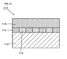
- the structure of the acoustic wave device described in Patent Document 2 is illustrated in Fig. 14 with a schematic front sectional view.
- an acoustic wave device 111 an IDT electrode 113 is formed on a piezoelectric substrate 112.
- a first insulation layer 114 having the same film thickness as the IDT electrode 113 is formed around a region where the IDT electrode 113 is present.
- a second insulator layer 115 is formed so as to cover the IDT electrode 113 and the first insulator layer 114.
- Patent Document 1 Japanese Unexamined Patent Application Publication No. 2004-112748
- Patent Document 2 WO 2005/034347 A1
- the insulator layer 104 in the surface acoustic wave device 101 described in Patent Document 1 has a sufficient thickness over a region where the IDT electrode 103 is present, the insertion loss tends to deteriorate.
- the thickness of the insulator layer 104 is increased in order to improve temperature characteristics, a problem exists in which the fractional bandwidth is reduced.
- the second insulator layer 115 formed on a region where the IDT electrode 113 is present has a reduced thickness to improve the temperature characteristics, it is difficult to improve the temperature characteristics using the second insulator layer 115.
- the second insulator layer 115 has a sufficiently increased thickness to improve the temperature characteristics, the thickness of the second insulator layer 115 over the IDT electrode 113 is increased, so a problem in which the fractional bandwidth is small exists.
- an object of the present invention to provide an acoustic wave device in which temperature characteristics are improved while the fractional bandwidth is less susceptible to being reduced without causing an increase in the insertion loss in a structure in which an insulation layer for improving the temperature characteristics is formed on an IDT electrode.
- an acoustic wave device including a piezoelectric substrate that includes a first main surface and a second main surface, at least one IDT electrode formed on the first main surface of the piezoelectric substrate, and an insulator layer for improving a temperature characteristic formed on the piezoelectric substrate so as to cover the IDT electrode.
- the wavelength of an acoustic wave is ⁇
- the height of the surface of the insulator layer in at least one portion of the second surface region is larger than the height of the surface of the insulator layer from the piezoelectric substrate in at least one portion of the first surface region by 0.001 ⁇ or more.
- the height of the surface of the insulator layer in at least one portion of the second surface region is larger than the height of the surface of the insulator layer in the first surface region by 0.001 ⁇ or more, and the height of the surface of the insulator layer in the second surface region is larger than the height of the insulator layer in at least one portion of the first surface region by 0.001 ⁇ or more.
- an acoustic wave device including a piezoelectric substrate that includes a first main surface and a second main surface, at least one IDT electrode formed on the first main surface of the piezoelectric substrate, and an insulator layer for improving a temperature characteristic formed on the piezoelectric substrate so as to cover the IDT electrode.
- the insulator layer includes a surface that has a projection protruding upward in at least one portion of a region under which no IDT electrode is positioned, and the height of the projection 7 from the surface of the insulator layer disposed around the projection is 0.001 ⁇ or more ( ⁇ is the wavelength of an acoustic wave).
- the insulator layer for improving the temperature characteristic is formed so as to cover the IDT electrode, and the surface of the insulator layer in the first surface region, under which the IDT electrode is positioned and that in the second surface region, under which no electrode is positioned, have different heights.
- the height of the surface of the insulator layer in at least one portion of the second surface region is larger than the height of the surface of the insulator layer from the piezoelectric substrate in at least one portion of the first surface region by 0.001 ⁇ or more.
- the upwardly protruding projection is disposed in at least one portion of the region under which no IDT electrode is positioned, i.e., of the second surface region in the first invention, and the height of the projection from the surface of the insulator layer disposed around the projection is 0.001 ⁇ or more.
- the present invention has the above-described configuration, so the insulator layer over the IDT electrode has a thinner portion. Therefore, the insertion loss is less prone to being degraded and the fractional bandwidth is less prone to being narrowed, while at the same time sufficient advantageous effects of improvement in the temperature characteristic are obtainable from the other thicker portion of the insulator layer.
- the insulator layer may include a first insulator layer and a second insulator layer, the first insulator layer being disposed around the IDT electrode and having a film thickness larger than that of the IDT electrode, the second insulator layer being disposed so as to cover the first insulator layer and the IDT electrode and having the same film thickness.
- the acoustic wave device according to the present invention can be easily provided merely by the formation of the second insulator layer having the same film thickness after the formation of the IDT electrode and the first insulator.
- the first and second insulator layers may be made of the same insulator material.
- the process can be simplified and the cost of manufacturing can be reduced.
- the first and second insulator layers may be made of different insulator materials.
- the piezoelectric substrate may be made of a piezoelectric material having a negative temperature coefficient of frequency
- the insulator layer for improving the temperature characteristic may be formed using silicon oxide.
- the insulator layer composed of silicon oxide and having a positive temperature coefficient of frequency can sufficiently reduce changes in frequency characteristic due to temperature.
- the IDT electrode may have a duty ratio of between 0.25 and 0.60, inclusive. This range of the duty ratio can avoid an increase in electric resistance of the IDT electrode, and according to the present invention, the temperature characteristic can be improved while the degradation of the insertion loss and the narrowing of the fractional bandwidth are prevented.
- the acoustic wave device can use various kinds of waves as an acoustic wave.
- a surface acoustic wave device which employs a surface acoustic wave, can be provided in accordance with the present invention.
- a method for fabricating an acoustic wave device includes he steps of forming an insulating material layer on a piezoelectric substrate, forming a patterned photoresist on the insulating material layer, patterning the insulating material layer, and forming a piezoelectric-substrate exposed depression corresponding to a region where an IDT electrode is to be formed on a first insulator layer composed of the insulating material layer, depositing a metallic material on the piezoelectric substrate to form the IDT electrode in the piezoelectric-substrate exposed depression such that the IDT electrode is thinner than the first insulator layer and coating the photoresist with a metallic film, removing the photoresist and the metallic layer on the photoresist by the lift-off technique, and depositing a second insulator layer so as to cover the IDT electrode and the first insulator layer.
- the surface of the insulator layer in at least one portion of the second surface region, under which no IDT electrode is positioned is higher than the surface of the other portion of the insulator layer by 0.001 ⁇ or more. Therefore, the temperature characteristic can be reliably improved due to the surface portion of the insulator layer having a sufficient thickness.
- the surface of the insulator layer in at least one portion of the first surface region is lower, as described above, and the insulator layer is thinner, the insertion loss is less prone to being degraded and the fractional bandwidth is less prone to being narrowed.
- the temperature characteristic can be improved without causing narrowing of the fractional bandwidth and an increase in the insertion loss.
- the patterned photoresist is formed on the insulating material layer, the laminated film in which the insulating material layer and the photoresist are laminated is patterned, and the first insulator layer having the piezoelectric-substrate exposed depression in which the IDT electrode is to be formed is formed.
- the metallic material is deposited so as to be thinner than the first insulator layer, thereby forming the IDT electrode in the piezoelectric-substrate exposed depression.
- the photoresist and the metallic film on the photoresist are removed by the lift-off technique, and finally, the second insulating material film is formed so as to cover the IDT electrode and the insulating material layer.
- the first insulator layer is thicker than the IDT electrode. Therefore, by deposition of the second insulating material layer, in accordance with the present invention, the acoustic wave device having the insulator layer being thin over the IDT electrode can be easily fabricated.
- Fig. 1(a) is a partial enlarged front sectional view that illustrates an enlarged portion of a region where an IDT electrode is formed in a surface acoustic wave device according to a first embodiment of the present invention
- Fig. 1(b) is a schematic plan view of the surface acoustic wave device.
- a surface acoustic wave device 1 is a one-port surface acoustic wave resonator, as illustrated in Fig. 1(b) .
- This surface acoustic wave resonator is used as one of a plurality of resonators constituting a band-pass filter at a transmission side of a duplexer of a mobile phone.
- the surface acoustic wave device 1 includes a piezoelectric substrate 2.
- the piezoelectric substrate 2 is made using, but not limited to, a 128° rotated Y-plate X-propagation LiNbO 3 substrate.
- An IDT electrode 3 is formed on the piezoelectric substrate 2.
- the IDT electrode 3 includes a pair of comb-shaped electrodes each having a plurality of electrode fingers 3a.
- a reflector 4 is disposed at one side of the IDT electrode 3
- a reflector 5 is disposed at the other side of the IDT electrode 3.
- Each of the reflectors 4 and 5 has a structure in which a plurality of electrode fingers are shorted at both ends.
- each of the IDT electrode 3 and the reflectors 4 and 5 is made of an electrode material principally composed of copper. More specifically, it has a laminated structure in which a thinner adhesion layer composed of titanium and disposed on the piezoelectric substrate 2, a main electrode layer composed of copper and formed on the adhesion layer, and a protective electrode layer composed of AlCu and laminated on the copper main electrode layer are laminated.
- the titanium adhesion layer has a thickness of 0.01 ⁇
- the main electrode layer has a thickness of 0.04 ⁇
- the protective electrode layer has a thickness of 0.005 ⁇ , where the wavelength of a surface acoustic wave is ⁇ .
- Each of the IDT electrode 3 and the reflectors 4 and 5 may also be composed of a single metallic layer. Alternatively, it may also have a structure in which a plurality of electrode layers are laminated, as in the present embodiment.
- the insulator layer 6 for improving temperature characteristics is formed so as to cover the IDT electrode 3 and the reflectors 4 and 5.
- the insulator layer 6 includes a first insulator layer 7 and a second insulator layer 8.
- the first insulator layer 7 is disposed around the IDT electrode 3, i.e., between the electrode fingers and in a region outside the electrode.
- the second insulator layer 8 is disposed so as to cover the first insulator layer 7 and the IDT electrode 3.
- the first insulator layer 7 is also formed around the reflectors 4 and 5, i.e., between the electrode fingers of the reflectors and in a region outside the reflectors.
- the second insulator layer 8 is also formed similarly.
- the thickness of the first insulator layer 7 is larger than that of the IDT electrode 3, i.e., that of the electrode.
- the difference in thickness therebetween is 0.001 ⁇ or more, where the wavelength of a surface acoustic wave is ⁇ .
- the second insulator layer 8 is provided by formation of an insulator layer having the same film thickness. Therefore, the second insulator layer 8 has a projection and a depression in its upper surface, as illustrated in the drawing.
- the upper-surface region of the insulator layer 6 is classified into a first surface region under which the IDT is disposed and a second surface region under which no IDT is disposed.
- the first insulator layer 7 is thicker than the IDT electrode 3
- the height of the surface of the insulator layer 6 in the second surface region is larger than the height of the surface of the insulator layer 6 from a top surface 2a of the piezoelectric substrate 2 in the first surface region, under which the IDT electrode 3 is disposed, by 0.001 ⁇ or more.
- a projection and a depression are disposed in the surface, i.e., the upper surface of the insulator layer 6, as illustrated in the drawing, and an upwardly protruding projection 6a is formed in the second surface region, under which no IDT electrode is disposed.
- the height of the projection 6a from the surface of the insulator layer formed around the projection 6a is 0.001 ⁇ or more.
- the surface of the insulator layer in the second surface region, around the region where the electrode is disposed is higher than the surface of the insulator layer in the first surface region, under which the electrode is disposed, by 0.001 ⁇ or more.
- the insulator layer disposed in the second surface region has a sufficient thickness. Therefore, the temperature characteristics can be effectively improved.
- the insulator layer is thinner over the IDT electrode 3, so the fractional bandwidth is less prone to being narrowed and the insertion loss is less prone to being degraded, as is obvious from an experimental example described later.
- Figs. 2(a) to 2(f) are partial front sectional view that schematically illustrate a method for fabricating the surface acoustic wave device 1.
- the piezoelectric substrate 2 composed of 128° rotated Y-plate X-propagation LiNbO 3 is prepared. Then, a SiO 2 film 7A is formed on the piezoelectric substrate 2 in order to form the first insulator layer 7 being thicker than the IDT electrode 3 by 0.001 ⁇ or more.
- a patterned photoresist 11 is formed by photolithography on a region around a region where the IDT electrode is to be formed.
- the patterned photoresist 11 covers the previously described second surface region.
- the SiO 2 film 7A that is not covered with the patterned photoresist 11, i.e., that is formed in the first surface region is removed by reactive ion etching, thus forming a piezoelectric-substrate exposed depression 12.
- the first insulator layer 7 is formed.
- a metallic film 3A is formed over the entire surface.
- the metallic film 3A is thinner than the first insulator layer 7.
- the portion of the metallic film applied on the piezoelectric-substrate exposed depression forms the IDT electrode 3.
- the metallic film 3A is obtained by sequentially depositing a Ti layer, a Cu layer, and an AlCu layer by a thin-film forming method, such as vapor deposition, as with the case of forming the IDT electrode 3 described above.
- the patterned photoresist 11 is removed by the lift-off technique together with the metallic film 3A formed on the patterned photoresist 11. As illustrated in Fig. 2(e) , a structure in which the IDT electrode 3 and the first insulator layer 7 are formed on the piezoelectric substrate 2 is obtained.
- the second insulator layer 8 composed of SiO 2 is formed over the entire surface. Because the first insulator layer 7 is thicker than the IDT electrode 3 by 0.001 ⁇ or more, as described above, the projection and depression having a substantially uniform shape are formed in the upper portion of the second insulator layer 8 along the width direction of interlocking of the IDT electrode, i.e., in a direction perpendicular to the sectional views of Figs. 2 by forming the second insulator layer 8 having the same film thickness by a commonly used thin-film forming method, such as vapor deposition or sputtering.
- a commonly used thin-film forming method such as vapor deposition or sputtering.
- the fabricating method described above uses photoresist etching.
- the method for fabricating the surface acoustic wave device 1 is not limited to the above-described fabricating method.
- the surface acoustic wave device 1 may be obtained by partially removing the surface of the insulator layer by, for example, etching, after the IDT electrode 3 and the insulator layer are formed on the piezoelectric substrate 2.
- the portion of the insulator layer removed by etching can be a portion over a region where the IDT electrode 3 is disposed.
- the first and second insulator layers are integrally made of the same material.
- the first insulator layer and the second insulator layer may be made of the same material, as described above. They may be individually formed of the same material, as in the embodiment previously described.
- the first insulator layer and the second insulator layer may also be made of different insulating materials. Forming the first and second insulator layers from the same insulating material can reduce kinds of materials and simplify the fabricating process.
- the insulating material of each of the first insulator layer and the second insulator layer is not particularly limited.
- silicon dioxide an oxide or a nitride of silicon, tantalum, aluminum, or other elements, for example SiO x N y or TaO x may be used.
- the electrode material of the IDT electrode is not particularly limited, so it is not limited to the material used in the above-described embodiment.
- the IDT electrode is not limited to a laminated film in which a plurality of electrode layers are laminated, so it may also be made of a single metallic material.
- the height of the insulator layer 6 from the top surface 2a of the piezoelectric substrate 2 in the first surface region was 0.27 ⁇ .
- the height of the insulator layer 6 in the second surface region was 0.27 ⁇ + x ⁇ .
- x i.e., the height of a projection of the insulator layer
- the duty of the IDT electrode 3 was 0.5.
- TCF The temperature coefficient of frequency TCF of each of a plurality of kinds of the surface acoustic wave device 1 prepared by the above-described way was measured. TCF was obtained by measurement of changes in resonant frequency due to temperature of the surface acoustic wave device 1 in a temperature range of -25°C to +85°C.
- TCF approaches 0 ppm/°C as the height x of the projection of the insulator layer increases. That is, it is found that changes in frequency characteristics due to temperature become smaller and the temperature characteristics are improved. In particular, it is found that, when x is 0.001 ⁇ or more, the advantageous effects of improvement in TCF are more evident.
- Figs. 5 illustrates changes in the impedance ratio in the surface acoustic wave device 1 i.e., the ratio of impedance at an antiresonant frequency to impedance at a resonant frequency with respect to the height x of the projection of the insulator layer.
- the impedance ratio changes.
- x is 0.001 ⁇ or more
- the impedance ratio is large, compared with a related-art example in which x is zero, thereby enabling the insertion loss to be effectively reduced.
- the temperature characteristics can be effectively improved without a significant reduction in the fractional bandwidth and in the impedance ratio.
- the height x of the projection of the insulator layer is 0.001 ⁇ or more.
- the surface acoustic wave device illustrated in Fig. 14 was fabricated in a similar manner to that of the above-described embodiment.
- a SiO 2 film for improving temperature characteristics having a film thickness of 0.27 ⁇ , 0.29 ⁇ , 0.31 ⁇ , or 0.33 ⁇ was formed as the second insulator layer. It is substantially the same as in the above-described embodiment except that the surface of the second insulator layer is flat.
- the temperature characteristic and the fractional bandwidth in the surface acoustic wave device according to this related-art example were measured in substantially the same manner as in the above-described embodiment. The results are shown in Figs. 6 and 7 .
- Figs. 6 and 7 illustrate changes in the temperature characteristic TCF and in the fractional bandwidth, respectively, with respect to the thickness of the second insulator layer in the surface acoustic wave device according to the related-art example prepared for comparison.
- Fig. 8 illustrates a relationship between the amount of improvement in temperature characteristic of frequency and the fractional bandwidth in the surface acoustic wave device 1 according to the above-described embodiment.
- a relationship between the amount of improvement in temperature characteristic of frequency and the fractional bandwidth in the surface acoustic wave device in the related art illustrated in Fig. 14 is also illustrated in Fig. 8 .
- the surface acoustic wave device illustrated in Fig. 13 in the related art was also fabricated in a similar manner to that of the above-described embodiment except that a SiO 2 film having a thickness of 0.27 ⁇ was formed over the entire surface so as to cover the IDT electrode.
- the impedance ratio was no more than 50 dB, which revealed that the characteristics were significantly exacerbated, compared with the above-described embodiment.
- the upper limit of the height x of the projection of the insulator layer i.e., the difference between the height of the surface of the insulator layer in the first surface region and that in the second surface region is 0.3 ⁇ .
- the upper limit is not limited to the above upper limit value, and the height x of the projection of the insulator layer can be 0.3 ⁇ or more.
- the insulator layer projects in the second surface region, compared with that in the first surface region, and the shape of the IDT electrode 3 in cross section in the cross-sectional direction is rectangular. However, it may be trapezoidal or inverted trapezoidal. The edges formed by the surface of the insulator layer and the projection may be rounded.
- a plurality of kinds of the surface acoustic wave device 1 having a height x of the projection of the insulator layer of 0.03 ⁇ and the duty ratio of the IDT electrode having different values were fabricated, and the temperature coefficient of frequency TCF was measured.
- the results are shown in Fig. 9 .
- the duty ratio is 0.60 or less, the absolute value of the temperature characteristic TCF can be smaller than -14 ppm/°C, and the temperature characteristics can be effectively improved.
- the duty ratio is less than 0.25, it is not preferred because the electric resistance is too high. Accordingly, it is preferable that the duty ratio be in a range of 0.25 to 0.6.
- the surface acoustic wave device 1 fabricated such that the height x of the projection of the insulator layer was 0.01 ⁇ , 0.02 ⁇ , or 0.03 ⁇
- the behavior of changes in resonant frequency immediately after a power of 0.9W was turned on was observed.
- the results are shown in Fig. 10 .
- the surface acoustic wave device having a height x of the projection of the insulator layer being zero, i.e., that corresponds to the related-art example illustrated in Fig. 14 was fabricated in a similar manner, and the amount of the frequency shift immediately after power was turned on was measured. The results are shown in Fig. 10 .
- Fig. 10 it is found that, when the height x of the projection of the insulator layer increases, the amount of the frequency shift occurring immediately after power is turned on reduces. That is, it is found that the withstand electric power is enhanced, and this can more suppress the frequency shift occurring immediately after power is turned on.
- the height x of the projection of the insulator layer is in a range of 0.01 ⁇ to 0.03 ⁇ , the amount of the frequency shift is significantly improved, and it is further improved when the height x of the projection of the insulator layer is in a range of 0.02 ⁇ to 0.03 ⁇ .
- a surface acoustic wave device having stable characteristics immediately after power is turned on is provided.
- the height of the insulator layer in the entire first surface region, under which the IDT electrode 3 is disposed is smaller than the height of the insulator layer in the entire second surface region, under which no IDT electrode 3 is disposed.
- the surface of the insulator layer in at least one portion of the second surface region may be higher than the surface of the insulator layer region in at least one portion of the first surface region by 0.001 ⁇ or more.
- the height of the insulator layer 6 in at least one portion of the first surface region over the IDT electrode 3 may be smaller than the height of the insulator layer in the second surface region.
- the dimension W of the projection 6a disposed in the surface of the insulator layer 6 along the dimensional width direction of electrode fingers may be larger than the gap between the electrode fingers.
- the surface of the insulator layer in at least one portion of the second surface region, under which no IDT electrode is disposed may be higher than the surface of the insulator layer in the first surface region.
- the width direction dimension W' of the projection 6a disposed in the surface of the insulator layer 6 may be smaller than the gap between the electrode fingers.
- a one-port surface acoustic wave resonator is described as one example.
- the present invention is applicable to a surface acoustic wave resonator having a different structure and a surface acoustic wave filter device and is also applicable to an acoustic wave device that uses an acoustic wave different from a surface acoustic wave, such as a boundary acoustic wave.
Landscapes
- Physics & Mathematics (AREA)
- Acoustics & Sound (AREA)
- Engineering & Computer Science (AREA)
- Manufacturing & Machinery (AREA)
- Surface Acoustic Wave Elements And Circuit Networks Thereof (AREA)
Abstract
Description
- The present invention relates to an acoustic wave device used as, for example, a resonator or a band-pass filter, and more specifically, to an acoustic wave device that has a structure in which an insulator layer for improving temperature characteristics is formed so as to cover an interdigital (IDT) electrode and to a method for fabricating the same.
- An acoustic wave resonator and an acoustic wave filter are widely used in a band-pass filter in a mobile communications device. One example of an acoustic wave device of this kind is disclosed in
Patent Document 1 described below.Fig. 13 is a front sectional view that schematically illustrates a surface acoustic wave device described inPatent Document 1. In a surfaceacoustic wave device 101 illustrated inFig. 13 , anIDT electrode 103 is formed on apiezoelectric substrate 102. Aninsulator layer 104 is formed so as to cover theIDT electrode 103. Here, thepiezoelectric substrate 102 is made of a piezoelectric material that has a negative temperature coefficient of frequency, such as a lithium tantalate (LiTaO3) substrate or a lithium niobate (LiNbO3) substrate. On the other hand, theinsulator layer 104 is made of an insulating material that has a positive temperature coefficient of frequency, such as silicon dioxide (SiO2). Consequently, according to this patent document, the surfaceacoustic wave device 101 having favorable temperature characteristics can be provided. - In the surface
acoustic wave device 101, theinsulator layer 104 made of, for example, a SiO2 film is formed after theIDT electrode 103 is formed. Therefore, when theinsulator layer 104 is formed by a thin-film forming method, such as vapor deposition, a projection and a depression, including a projection 104a and adepression 104b, are inevitably formed. This is because theIDT electrode 103 is present under theinsulator layer 104 and thus the surface of theinsulator layer 104 is high at a region where theIDT electrode 103 is present, so this results in the projection 104a. - However, when the projection and depression are formed, an unwanted ripple appears in the frequency characteristics. An acoustic wave device that has no such projection and depression is disclosed in
Patent Document 2 described below. The structure of the acoustic wave device described inPatent Document 2 is illustrated inFig. 14 with a schematic front sectional view. In an acoustic wave device 111, anIDT electrode 113 is formed on apiezoelectric substrate 112. Afirst insulation layer 114 having the same film thickness as theIDT electrode 113 is formed around a region where theIDT electrode 113 is present. Asecond insulator layer 115 is formed so as to cover theIDT electrode 113 and thefirst insulator layer 114. Here, after thefirst insulator layer 114 and theIDT electrode 113 is formed, thesecond insulator layer 115 is formed. As a result, thesecond insulator layer 115 has a surface 115a having no projection and depression, so thesecond insulator layer 115 is flat. Patent Document 1: Japanese Unexamined Patent Application Publication No.2004-112748
Patent Document 2:WO 2005/034347 A1 - Because the
insulator layer 104 in the surfaceacoustic wave device 101 described inPatent Document 1 has a sufficient thickness over a region where theIDT electrode 103 is present, the insertion loss tends to deteriorate. In addition, when the thickness of theinsulator layer 104 is increased in order to improve temperature characteristics, a problem exists in which the fractional bandwidth is reduced. - If, in the
acoustic wave device 114 described inPatent Document 2, thesecond insulator layer 115 formed on a region where theIDT electrode 113 is present has a reduced thickness to improve the temperature characteristics, it is difficult to improve the temperature characteristics using thesecond insulator layer 115. On the other hand, if thesecond insulator layer 115 has a sufficiently increased thickness to improve the temperature characteristics, the thickness of thesecond insulator layer 115 over theIDT electrode 113 is increased, so a problem in which the fractional bandwidth is small exists. - That is, in the surface
acoustic wave device 101 or 111 described inPatent Document insulator layer IDT electrode 103 is reduced to avoid this problem, the temperature characteristics cannot be sufficiently improved. - In light of the above-described current circumstances in the related art, it is an object of the present invention to provide an acoustic wave device in which temperature characteristics are improved while the fractional bandwidth is less susceptible to being reduced without causing an increase in the insertion loss in a structure in which an insulation layer for improving the temperature characteristics is formed on an IDT electrode.
- According to a first invention, provided is an acoustic wave device including a piezoelectric substrate that includes a first main surface and a second main surface, at least one IDT electrode formed on the first main surface of the piezoelectric substrate, and an insulator layer for improving a temperature characteristic formed on the piezoelectric substrate so as to cover the IDT electrode. Where the wavelength of an acoustic wave is λ, when a surface of the insulator layer is classified into a first surface region under which the IDT electrode is positioned and a second surface region under which no IDT electrode is positioned, the height of the surface of the insulator layer in at least one portion of the second surface region is larger than the height of the surface of the insulator layer from the piezoelectric substrate in at least one portion of the first surface region by 0.001λ or more. Specifically, the height of the surface of the insulator layer in at least one portion of the second surface region is larger than the height of the surface of the insulator layer in the first surface region by 0.001λ or more, and the height of the surface of the insulator layer in the second surface region is larger than the height of the insulator layer in at least one portion of the first surface region by 0.001λ or more.
- According to a second invention, provided is an acoustic wave device including a piezoelectric substrate that includes a first main surface and a second main surface, at least one IDT electrode formed on the first main surface of the piezoelectric substrate, and an insulator layer for improving a temperature characteristic formed on the piezoelectric substrate so as to cover the IDT electrode. The insulator layer includes a surface that has a projection protruding upward in at least one portion of a region under which no IDT electrode is positioned, and the height of the
projection 7 from the surface of the insulator layer disposed around the projection is 0.001λ or more (λ is the wavelength of an acoustic wave). - That is, in the first and second inventions (hereinafter referred to collectively as the present invention as necessary), the insulator layer for improving the temperature characteristic is formed so as to cover the IDT electrode, and the surface of the insulator layer in the first surface region, under which the IDT electrode is positioned and that in the second surface region, under which no electrode is positioned, have different heights. In the first invention, the height of the surface of the insulator layer in at least one portion of the second surface region is larger than the height of the surface of the insulator layer from the piezoelectric substrate in at least one portion of the first surface region by 0.001λ or more. In the description of the second invention, the upwardly protruding projection is disposed in at least one portion of the region under which no IDT electrode is positioned, i.e., of the second surface region in the first invention, and the height of the projection from the surface of the insulator layer disposed around the projection is 0.001λ or more.
- According to the present invention, it has the above-described configuration, so the insulator layer over the IDT electrode has a thinner portion. Therefore, the insertion loss is less prone to being degraded and the fractional bandwidth is less prone to being narrowed, while at the same time sufficient advantageous effects of improvement in the temperature characteristic are obtainable from the other thicker portion of the insulator layer.
- The structure of the insulator layer for improving the temperature characteristic is not particularly limited. According to a specific aspect of the present invention, the insulator layer may include a first insulator layer and a second insulator layer, the first insulator layer being disposed around the IDT electrode and having a film thickness larger than that of the IDT electrode, the second insulator layer being disposed so as to cover the first insulator layer and the IDT electrode and having the same film thickness. In this case, the acoustic wave device according to the present invention can be easily provided merely by the formation of the second insulator layer having the same film thickness after the formation of the IDT electrode and the first insulator.
- Preferably, the first and second insulator layers may be made of the same insulator material. In this case, because the first insulator layer and the second insulator layer can be made of the same material, the process can be simplified and the cost of manufacturing can be reduced. Of cause, the first and second insulator layers may be made of different insulator materials.
- In the acoustic wave device according to the present invention, preferably, the piezoelectric substrate may be made of a piezoelectric material having a negative temperature coefficient of frequency, and the insulator layer for improving the temperature characteristic may be formed using silicon oxide. In this case, the insulator layer composed of silicon oxide and having a positive temperature coefficient of frequency can sufficiently reduce changes in frequency characteristic due to temperature.
- In the present invention, preferably, the IDT electrode may have a duty ratio of between 0.25 and 0.60, inclusive. This range of the duty ratio can avoid an increase in electric resistance of the IDT electrode, and according to the present invention, the temperature characteristic can be improved while the degradation of the insertion loss and the narrowing of the fractional bandwidth are prevented.
- The acoustic wave device according to the present invention can use various kinds of waves as an acoustic wave. For example, a surface acoustic wave device, which employs a surface acoustic wave, can be provided in accordance with the present invention.
- A method for fabricating an acoustic wave device according the present invention includes he steps of forming an insulating material layer on a piezoelectric substrate, forming a patterned photoresist on the insulating material layer, patterning the insulating material layer, and forming a piezoelectric-substrate exposed depression corresponding to a region where an IDT electrode is to be formed on a first insulator layer composed of the insulating material layer, depositing a metallic material on the piezoelectric substrate to form the IDT electrode in the piezoelectric-substrate exposed depression such that the IDT electrode is thinner than the first insulator layer and coating the photoresist with a metallic film, removing the photoresist and the metallic layer on the photoresist by the lift-off technique, and depositing a second insulator layer so as to cover the IDT electrode and the first insulator layer.
- In the acoustic wave device according to the first invention and the acoustic wave device according to the second invention, the surface of the insulator layer in at least one portion of the second surface region, under which no IDT electrode is positioned, is higher than the surface of the other portion of the insulator layer by 0.001λ or more. Therefore, the temperature characteristic can be reliably improved due to the surface portion of the insulator layer having a sufficient thickness. In addition, because the surface of the insulator layer in at least one portion of the first surface region is lower, as described above, and the insulator layer is thinner, the insertion loss is less prone to being degraded and the fractional bandwidth is less prone to being narrowed.
- Accordingly, the temperature characteristic can be improved without causing narrowing of the fractional bandwidth and an increase in the insertion loss.
- With the method for fabricating an acoustic wave device according to the present invention, after the completion of the insulating material layer on the piezoelectric substrate, the patterned photoresist is formed on the insulating material layer, the laminated film in which the insulating material layer and the photoresist are laminated is patterned, and the first insulator layer having the piezoelectric-substrate exposed depression in which the IDT electrode is to be formed is formed. Then, the metallic material is deposited so as to be thinner than the first insulator layer, thereby forming the IDT electrode in the piezoelectric-substrate exposed depression. The photoresist and the metallic film on the photoresist are removed by the lift-off technique, and finally, the second insulating material film is formed so as to cover the IDT electrode and the insulating material layer. In this case, the first insulator layer is thicker than the IDT electrode. Therefore, by deposition of the second insulating material layer, in accordance with the present invention, the acoustic wave device having the insulator layer being thin over the IDT electrode can be easily fabricated.
-
-
Fig. 1(a) is a schematic front sectional view that illustrates a main portion of a surface acoustic wave device according to an embodiment of the present invention, andFig. 1(b) is a plan view of the surface acoustic wave device. -
Figs. 2(a) to (f) are schematic front sectional views for describing steps of fabricating a surface acoustic wave device according to an embodiment of the present invention. -
Fig. 3(a) illustrates a relationship between the height x of a projection of an insulator layer and the temperature characteristic TCF in the surface acoustic wave device according to the embodiment, andFig. 3(b) illustrates an enlarged portion thereof. -
Fig. 4(a) illustrates a relationship between the height x of a projection of an insulator layer and the fractional bandwidth BW in the surface acoustic wave device according to the embodiment, andFig. 4(b) illustrates an enlarged portion thereof. -
Fig. 5(a) illustrates a relationship between the height x of a projection of an insulator layer and the impedance ratio in the surface acoustic wave device according to the embodiment, andFig. 5(b) illustrates an enlarged portion thereof. -
Fig. 5 illustrates a relationship between the thickness of a second insulator layer and the temperature characteristic TCF in a related-art surface acoustic wave device prepared for comparison. -
Fig. 7 illustrates a relationship between the thickness of a second insulator layer and the fractional bandwidth BW in the related-art surface acoustic wave device prepared for comparison. -
Fig. 8 illustrates a relationship between the amount of improvement in the temperature characteristic and the fractional bandwidth in each of the surface acoustic wave device according to the embodiment and that according to a related-art example. -
Fig. 9 illustrates a relationship between the duty of an IDT electrode and the temperature characteristic in the surface acoustic wave device according to the embodiment. -
Fig. 10 illustrates a relationship between the height x of a projection of a surface of an insulator layer and the amount of a frequency shift immediately after power is turned on. -
Fig. 11 is a schematic front sectional view for describing the surface acoustic wave device according to one modification example of the present invention. -
Fig. 12 is a schematic front sectional view for describing the surface acoustic wave device according to another modification example of the present invention. -
Fig. 13 is a schematic front sectional view that illustrates one example of a related-art surface acoustic wave device. -
Fig. 14 is a schematic front sectional view that illustrates another example of the related-art surface acoustic wave device. -
- 1
- surface acoustic wave device
- 2
- piezoelectric substrate
- 3
- IDT electrode
- 3a
- electrode finger
- 3A
- metallic film
- 4, 5
- reflector
- 6
- insulator layer
- 6a
- projection
- 7
- first insulator layer
- 7A
- SiO2 film
- 8
- second insulator layer
- Specific embodiments of the present invention will be described below with reference to the drawings.
-
Fig. 1(a) is a partial enlarged front sectional view that illustrates an enlarged portion of a region where an IDT electrode is formed in a surface acoustic wave device according to a first embodiment of the present invention, andFig. 1(b) is a schematic plan view of the surface acoustic wave device. - A surface
acoustic wave device 1 according to the present embodiment is a one-port surface acoustic wave resonator, as illustrated inFig. 1(b) . This surface acoustic wave resonator is used as one of a plurality of resonators constituting a band-pass filter at a transmission side of a duplexer of a mobile phone. - As illustrated in
Fig. 1(b) , the surfaceacoustic wave device 1 includes apiezoelectric substrate 2. Thepiezoelectric substrate 2 is made using, but not limited to, a 128° rotated Y-plate X-propagation LiNbO3 substrate. - An
IDT electrode 3 is formed on thepiezoelectric substrate 2. TheIDT electrode 3 includes a pair of comb-shaped electrodes each having a plurality of electrode fingers 3a. In the direction of propagation of a surface acoustic wave, areflector 4 is disposed at one side of theIDT electrode 3, and areflector 5 is disposed at the other side of theIDT electrode 3. Each of thereflectors - In the present embodiment, each of the
IDT electrode 3 and thereflectors piezoelectric substrate 2, a main electrode layer composed of copper and formed on the adhesion layer, and a protective electrode layer composed of AlCu and laminated on the copper main electrode layer are laminated. In the present embodiment, the titanium adhesion layer has a thickness of 0.01λ, the main electrode layer has a thickness of 0.04λ, and the protective electrode layer has a thickness of 0.005λ, where the wavelength of a surface acoustic wave is λ. - Each of the
IDT electrode 3 and thereflectors - An
insulator layer 6 for improving temperature characteristics is formed so as to cover theIDT electrode 3 and thereflectors insulator layer 6 includes afirst insulator layer 7 and asecond insulator layer 8. Thefirst insulator layer 7 is disposed around theIDT electrode 3, i.e., between the electrode fingers and in a region outside the electrode. Thesecond insulator layer 8 is disposed so as to cover thefirst insulator layer 7 and theIDT electrode 3. Thefirst insulator layer 7 is also formed around thereflectors second insulator layer 8 is also formed similarly. - The thickness of the
first insulator layer 7 is larger than that of theIDT electrode 3, i.e., that of the electrode. The difference in thickness therebetween is 0.001λ or more, where the wavelength of a surface acoustic wave is λ. - The
second insulator layer 8 is provided by formation of an insulator layer having the same film thickness. Therefore, thesecond insulator layer 8 has a projection and a depression in its upper surface, as illustrated in the drawing. The upper-surface region of theinsulator layer 6 is classified into a first surface region under which the IDT is disposed and a second surface region under which no IDT is disposed. In this case, because thefirst insulator layer 7 is thicker than theIDT electrode 3, the height of the surface of theinsulator layer 6 in the second surface region is larger than the height of the surface of theinsulator layer 6 from atop surface 2a of thepiezoelectric substrate 2 in the first surface region, under which theIDT electrode 3 is disposed, by 0.001λ or more. - In other words, a projection and a depression are disposed in the surface, i.e., the upper surface of the
insulator layer 6, as illustrated in the drawing, and an upwardlyprotruding projection 6a is formed in the second surface region, under which no IDT electrode is disposed. The height of theprojection 6a from the surface of the insulator layer formed around theprojection 6a is 0.001λ or more. - Similarly, also in the region where the
reflectors - As described above, in the surface
acoustic wave device 1 according to the present embodiment, the insulator layer disposed in the second surface region has a sufficient thickness. Therefore, the temperature characteristics can be effectively improved. The insulator layer is thinner over theIDT electrode 3, so the fractional bandwidth is less prone to being narrowed and the insertion loss is less prone to being degraded, as is obvious from an experimental example described later. - One example of a method for fabricating the surface
acoustic wave device 1 will now be described with reference toFigs. 2 . -
Figs. 2(a) to 2(f) are partial front sectional view that schematically illustrate a method for fabricating the surfaceacoustic wave device 1. - First, as illustrated in
Fig. 2(a) , thepiezoelectric substrate 2 composed of 128° rotated Y-plate X-propagation LiNbO3 is prepared. Then, a SiO2 film 7A is formed on thepiezoelectric substrate 2 in order to form thefirst insulator layer 7 being thicker than theIDT electrode 3 by 0.001λ or more. - After that, as illustrated in
Fig. 2(b) , a patternedphotoresist 11 is formed by photolithography on a region around a region where the IDT electrode is to be formed. The patternedphotoresist 11 covers the previously described second surface region. - After that, as illustrated in
Fig. 2(c) , the SiO2 film 7A that is not covered with the patternedphotoresist 11, i.e., that is formed in the first surface region is removed by reactive ion etching, thus forming a piezoelectric-substrate exposeddepression 12. In such a way, thefirst insulator layer 7 is formed. - Then, as illustrated in
Fig. 2(d) , in order to form theIDT electrode 3, ametallic film 3A is formed over the entire surface. Themetallic film 3A is thinner than thefirst insulator layer 7. The portion of the metallic film applied on the piezoelectric-substrate exposed depression forms theIDT electrode 3. Themetallic film 3A is obtained by sequentially depositing a Ti layer, a Cu layer, and an AlCu layer by a thin-film forming method, such as vapor deposition, as with the case of forming theIDT electrode 3 described above. - Then, the patterned
photoresist 11 is removed by the lift-off technique together with themetallic film 3A formed on the patternedphotoresist 11. As illustrated inFig. 2(e) , a structure in which theIDT electrode 3 and thefirst insulator layer 7 are formed on thepiezoelectric substrate 2 is obtained. - After that, as illustrated in
Fig. 2(f) , thesecond insulator layer 8 composed of SiO2 is formed over the entire surface. Because thefirst insulator layer 7 is thicker than theIDT electrode 3 by 0.001λ or more, as described above, the projection and depression having a substantially uniform shape are formed in the upper portion of thesecond insulator layer 8 along the width direction of interlocking of the IDT electrode, i.e., in a direction perpendicular to the sectional views ofFigs. 2 by forming thesecond insulator layer 8 having the same film thickness by a commonly used thin-film forming method, such as vapor deposition or sputtering. - The fabricating method described above uses photoresist etching. However, the method for fabricating the surface
acoustic wave device 1 is not limited to the above-described fabricating method. For example, the surfaceacoustic wave device 1 may be obtained by partially removing the surface of the insulator layer by, for example, etching, after theIDT electrode 3 and the insulator layer are formed on thepiezoelectric substrate 2. In this case, the portion of the insulator layer removed by etching can be a portion over a region where theIDT electrode 3 is disposed. In this case, the first and second insulator layers are integrally made of the same material. - The first insulator layer and the second insulator layer may be made of the same material, as described above. They may be individually formed of the same material, as in the embodiment previously described. The first insulator layer and the second insulator layer may also be made of different insulating materials. Forming the first and second insulator layers from the same insulating material can reduce kinds of materials and simplify the fabricating process.
- The insulating material of each of the first insulator layer and the second insulator layer is not particularly limited. In addition to silicon dioxide, an oxide or a nitride of silicon, tantalum, aluminum, or other elements, for example SiOxNy or TaOx may be used.
- The electrode material of the IDT electrode is not particularly limited, so it is not limited to the material used in the above-described embodiment. The IDT electrode is not limited to a laminated film in which a plurality of electrode layers are laminated, so it may also be made of a single metallic material.
- In the surface
acoustic wave device 1 described above, the height of theinsulator layer 6 from thetop surface 2a of thepiezoelectric substrate 2 in the first surface region was 0.27λ. The height of theinsulator layer 6 in the second surface region was 0.27λ + xλ. As illustrated inFig. 3 , by variously changing x, i.e., the height of a projection of the insulator layer, this height corresponding to the height of the insulator layer in the second surface region minus the height of the insulator layer in the first surface region a plurality of kinds of the surfaceacoustic wave device 1 were fabricated. - The duty of the
IDT electrode 3 was 0.5. - The temperature coefficient of frequency TCF of each of a plurality of kinds of the surface
acoustic wave device 1 prepared by the above-described way was measured. TCF was obtained by measurement of changes in resonant frequency due to temperature of the surfaceacoustic wave device 1 in a temperature range of -25°C to +85°C. - As is obvious from
Figs. 3(a) and 3(b) , it found that TCF approaches 0 ppm/°C as the height x of the projection of the insulator layer increases. That is, it is found that changes in frequency characteristics due to temperature become smaller and the temperature characteristics are improved. In particular, it is found that, when x is 0.001λ or more, the advantageous effects of improvement in TCF are more evident. - Changes in the fractional bandwidth with respect to the height x of the projection of the insulator layer of the surface
acoustic wave device 1 are illustrated inFigs. 4 . - As is obvious from
Figs. 4(a) and 4(b) , it is found that the fractional bandwidth tends to reduce with an increase in the height x of the projection of the insulator layer. However, as is obvious from the comparison betweenFigs. 3 and4 , when the height of the projection of the insulator layer increases, the advantageous effects of improvement in temperature characteristics are large, whereas the fractional bandwidth does not significantly reduce. -
Figs. 5 illustrates changes in the impedance ratio in the surfaceacoustic wave device 1 i.e., the ratio of impedance at an antiresonant frequency to impedance at a resonant frequency with respect to the height x of the projection of the insulator layer. - As is obvious from
Figs. 5 , when the height x of the projection of the insulator layer changes, the impedance ratio changes. When x is 0.001λ or more, the impedance ratio is large, compared with a related-art example in which x is zero, thereby enabling the insertion loss to be effectively reduced. - As described above, compared with when the height of the projection of the insulator layer is zero, i.e., compared with a structure corresponding to the related-art example illustrated in
Fig. 14 , if the height x of the projection of the insulator layer is 0.001λ or more, the temperature characteristics can be effectively improved without a significant reduction in the fractional bandwidth and in the impedance ratio. - Accordingly, as is obvious from
Figs. 3 to 5 , in the present embodiment, the height x of the projection of the insulator layer is 0.001λ or more. - For comparison, the surface acoustic wave device illustrated in
Fig. 14 was fabricated in a similar manner to that of the above-described embodiment. In the surfaceacoustic wave device 1 in the comparison example, a SiO2 film for improving temperature characteristics having a film thickness of 0.27λ, 0.29λ, 0.31λ, or 0.33λ was formed as the second insulator layer. It is substantially the same as in the above-described embodiment except that the surface of the second insulator layer is flat. The temperature characteristic and the fractional bandwidth in the surface acoustic wave device according to this related-art example were measured in substantially the same manner as in the above-described embodiment. The results are shown inFigs. 6 and 7 . -
Figs. 6 and 7 illustrate changes in the temperature characteristic TCF and in the fractional bandwidth, respectively, with respect to the thickness of the second insulator layer in the surface acoustic wave device according to the related-art example prepared for comparison. - As is obvious from
Figs. 6 and 7 , it is found that, in the surface acoustic wave device corresponding to the related-art example illustrated inFig. 14 , as the thickness of the second insulator layer increases, the temperature characteristic are improved, whereas the fractional bandwidth is shapely narrowed. - In contrast to this, as illustrated in
Figs. 3 to 5 , it is found that, in the surfaceacoustic wave device 1 according to the present embodiment, as previously described, even when the advantageous effects of improvement in the temperature characteristics are sufficiently obtained from the thicker insulator layer in the second surface region, under which no IDT electrode is disposed, the fractional bandwidth is less prone to being narrowed, the impedance ratio is less prone to being reduced, and therefore the insertion loss is less prone to being exacerbated. This is because the fractional bandwidth is less prone to being narrowed and the impedance ratio is less prone to being reduced due to a smaller thickness of the insulator layer over the IDT electrode, whereas the advantageous effects of improvement in the temperature characteristics are sufficiently obtained from a larger thickness of the insulator layer in the second surface region, under which no IDT electrode is disposed. -
Fig. 8 illustrates a relationship between the amount of improvement in temperature characteristic of frequency and the fractional bandwidth in the surfaceacoustic wave device 1 according to the above-described embodiment. InFig. 8 , the vertical axis represents a normalized fractional bandwidth relative to a fractional bandwidth in a surface acoustic wave device in which the insulator layer for improving the temperature characteristic is 0.27λ and the surface of the insulator layer is flat (x=0). - For comparison, a relationship between the amount of improvement in temperature characteristic of frequency and the fractional bandwidth in the surface acoustic wave device in the related art illustrated in
Fig. 14 is also illustrated inFig. 8 . - As is obvious from
Fig. 8 , it is found that, in the surface acoustic wave device in the related art illustrated inFig. 14 , when the temperature characteristics are improved, the fractional bandwidth significantly reduces with an increase in the amount of improvement in temperature characteristic of frequency and, in contrast to this, according to the above-described embodiment, even when the amount of improvement in the temperature characteristic is increased, the fractional bandwidth is less prone to being narrowed. - The surface acoustic wave device illustrated in
Fig. 13 in the related art was also fabricated in a similar manner to that of the above-described embodiment except that a SiO2 film having a thickness of 0.27λ was formed over the entire surface so as to cover the IDT electrode. The impedance ratio was no more than 50 dB, which revealed that the characteristics were significantly exacerbated, compared with the above-described embodiment. - In the above-described embodiment, it is difficult for the fabricating method described with reference to
Fig. 2 to form theinsulator layer 6 such that the height x of the projection of the insulator layer is 0.3λ or more for process reasons. Accordingly, for manufacturing reasons, the upper limit of the height x of the projection of the insulator layer, i.e., the difference between the height of the surface of the insulator layer in the first surface region and that in the second surface region is 0.3λ. When the surfaceacoustic wave device 1 is obtained using a fabricating method other than the above-described fabricating method, the upper limit is not limited to the above upper limit value, and the height x of the projection of the insulator layer can be 0.3λ or more. - In the above-described embodiment, for the projection and depression in the surface of the
insulator layer 6, the insulator layer projects in the second surface region, compared with that in the first surface region, and the shape of theIDT electrode 3 in cross section in the cross-sectional direction is rectangular. However, it may be trapezoidal or inverted trapezoidal. The edges formed by the surface of the insulator layer and the projection may be rounded. - In the forgoing surface
acoustic wave device 1, a plurality of kinds of the surfaceacoustic wave device 1 having a height x of the projection of the insulator layer of 0.03λ and the duty ratio of the IDT electrode having different values were fabricated, and the temperature coefficient of frequency TCF was measured. The results are shown inFig. 9 . As is obvious fromFig. 9 , it is found that, when the duty ratio is 0.60 or less, the absolute value of the temperature characteristic TCF can be smaller than -14 ppm/°C, and the temperature characteristics can be effectively improved. When the duty ratio is less than 0.25, it is not preferred because the electric resistance is too high. Accordingly, it is preferable that the duty ratio be in a range of 0.25 to 0.6. - Next, in the surface
acoustic wave device 1 according to the above-described embodiment fabricated such that the height x of the projection of the insulator layer was 0.01λ, 0.02λ, or 0.03λ, the behavior of changes in resonant frequency immediately after a power of 0.9W was turned on was observed. The results are shown inFig. 10 . For comparison, the surface acoustic wave device having a height x of the projection of the insulator layer being zero, i.e., that corresponds to the related-art example illustrated inFig. 14 was fabricated in a similar manner, and the amount of the frequency shift immediately after power was turned on was measured. The results are shown inFig. 10 . - As is obvious from
Fig. 10 , it is found that, when the height x of the projection of the insulator layer increases, the amount of the frequency shift occurring immediately after power is turned on reduces. That is, it is found that the withstand electric power is enhanced, and this can more suppress the frequency shift occurring immediately after power is turned on. In particular, when the height x of the projection of the insulator layer is in a range of 0.01λ to 0.03λ, the amount of the frequency shift is significantly improved, and it is further improved when the height x of the projection of the insulator layer is in a range of 0.02λ to 0.03λ. - Therefore, it is found that, according to the present invention, a surface acoustic wave device having stable characteristics immediately after power is turned on is provided.
- In the surface
acoustic wave device 1 illustrated inFig. 1(a) , the height of the insulator layer in the entire first surface region, under which theIDT electrode 3 is disposed, is smaller than the height of the insulator layer in the entire second surface region, under which noIDT electrode 3 is disposed. However, in the present invention, the surface of the insulator layer in at least one portion of the second surface region may be higher than the surface of the insulator layer region in at least one portion of the first surface region by 0.001λ or more. As a result, as illustrated inFig. 11 , the height of theinsulator layer 6 in at least one portion of the first surface region over theIDT electrode 3 may be smaller than the height of the insulator layer in the second surface region. In other words, the dimension W of theprojection 6a disposed in the surface of theinsulator layer 6 along the dimensional width direction of electrode fingers may be larger than the gap between the electrode fingers. - As illustrated in
Fig. 12 , the surface of the insulator layer in at least one portion of the second surface region, under which no IDT electrode is disposed, may be higher than the surface of the insulator layer in the first surface region. In other words, the width direction dimension W' of theprojection 6a disposed in the surface of theinsulator layer 6 may be smaller than the gap between the electrode fingers. - In the above-described embodiment, a one-port surface acoustic wave resonator is described as one example. However, the present invention is applicable to a surface acoustic wave resonator having a different structure and a surface acoustic wave filter device and is also applicable to an acoustic wave device that uses an acoustic wave different from a surface acoustic wave, such as a boundary acoustic wave.
Claims (9)
- An acoustic wave device comprising:a piezoelectric substrate that includes a first main surface and a second main surface;at least one interdigital transducer (IDT) electrode formed on the first main surface of the piezoelectric substrate; andan insulator layer for improving a temperature characteristic formed on the piezoelectric substrate so as to cover the IDT electrode;wherein, where the wavelength of an acoustic wave is λ, when a surface of the insulator layer is classified into a first surface region under which the IDT electrode is positioned and a second surface region under which no IDT electrode is positioned, the height of the surface of the insulator layer in at least one portion of the second surface region is larger than the height of the surface of the insulator layer from the piezoelectric substrate in at least one portion of the first surface region by 0.001λ or more.
- An acoustic wave device comprising:a piezoelectric substrate that includes a first main surface and a second main surface;at least one interdigital transducer (IDT) electrode formed on the first main surface of the piezoelectric substrate; andan insulator layer for improving a temperature characteristic formed on the piezoelectric substrate so as to cover the IDT electrode;wherein the insulator layer includes a surface that has a projection protruding upward in at least one portion of a region under which no IDT electrode is positioned, and the height of the projection 7 from the surface of the insulator layer disposed around the projection is 0.001λ or more (λ is the wavelength of an acoustic wave).
- The acoustic wave device according to Claim 1 or 2, wherein the insulator layer includes a first insulator layer and a second insulator layer, the first insulator layer being disposed around the IDT electrode and having a film thickness larger than the thickness of the IDT electrode, the second insulator layer being disposed so as to cover the first insulator layer and the IDT electrode and having the same film thickness.
- The acoustic wave device according to Claim 3, wherein the first and second insulator layers are made of the same insulator material.
- The acoustic wave device according to Claim 3, wherein the first and second insulator layers are made of different insulator materials.
- The acoustic wave device according to any one of Claims 1 to 5, wherein the piezoelectric substrate is made of a piezoelectric material having a negative temperature coefficient of frequency, and the insulator layer for improving the temperature characteristic is formed using silicon oxide.
- The acoustic wave device according to any one of Claims 1 to 7, wherein the IDT electrode has a duty ratio of between 0.25 and 0.60, inclusive.
- The acoustic wave device according to any one of Claims 1 to 7, wherein the acoustic wave device is a surface acoustic wave device, which uses a surface acoustic wave.
- A method for fabricating an acoustic wave device, the method comprising the steps of:forming an insulating material layer on a piezoelectric substrate;forming a patterned photoresist on the insulating material layer, patterning the insulating material layer, and forming a piezoelectric-substrate exposed depression corresponding to a region where an IDT electrode is to be formed on a first insulator layer composed of the insulating material layer;depositing a metallic material on the piezoelectric substrate to form the IDT electrode in the piezoelectric-substrate exposed depression such that the IDT electrode is thinner than the first insulator layer and coating the photoresist with a metallic film;removing the photoresist and the metallic layer on the photoresist by the lift-off technique; anddepositing a second insulator layer so as to cover the IDT electrode and the first insulator layer.
Applications Claiming Priority (2)
| Application Number | Priority Date | Filing Date | Title |
|---|---|---|---|
| JP2006056378 | 2006-03-02 | ||
| PCT/JP2007/051995 WO2007099742A1 (en) | 2006-03-02 | 2007-02-06 | Acoustic wave device and method for fabricating the same |
Publications (3)
| Publication Number | Publication Date |
|---|---|
| EP1990915A1 true EP1990915A1 (en) | 2008-11-12 |
| EP1990915A4 EP1990915A4 (en) | 2010-03-31 |
| EP1990915B1 EP1990915B1 (en) | 2017-11-01 |
Family
ID=38458862
Family Applications (1)
| Application Number | Title | Priority Date | Filing Date |
|---|---|---|---|
| EP07713837.8A Active EP1990915B1 (en) | 2006-03-02 | 2007-02-06 | Acoustic wave device and method for fabricating the same |
Country Status (6)
| Country | Link |
|---|---|
| US (3) | US7701113B2 (en) |
| EP (1) | EP1990915B1 (en) |
| JP (1) | JPWO2007099742A1 (en) |
| KR (1) | KR100954688B1 (en) |
| CN (1) | CN101395796B (en) |
| WO (1) | WO2007099742A1 (en) |
Families Citing this family (12)
| Publication number | Priority date | Publication date | Assignee | Title |
|---|---|---|---|---|
| WO2007099742A1 (en) * | 2006-03-02 | 2007-09-07 | Murata Manufacturing Co., Ltd. | Acoustic wave device and method for fabricating the same |
| CN101485086B (en) * | 2006-07-05 | 2012-06-13 | 株式会社村田制作所 | Surface Acoustic Wave Device |
| JP5339582B2 (en) * | 2008-07-31 | 2013-11-13 | 太陽誘電株式会社 | Elastic wave device |
| WO2011018913A1 (en) * | 2009-08-10 | 2011-02-17 | 株式会社村田製作所 | Boundary acoustic wave device |
| CN102684639B (en) * | 2011-03-07 | 2016-08-17 | 特里奎恩特半导体公司 | Make the acoustic duct Apparatus and method for that fine setting impact and piston mode unstability minimize |
| US9232315B2 (en) | 2011-03-16 | 2016-01-05 | Phonon Corporation | Monolithically applied heating elements on saw substrate |
| WO2012124210A1 (en) * | 2011-03-16 | 2012-09-20 | 株式会社村田製作所 | Method for producing elastic wave device |
| US9742373B2 (en) * | 2011-10-31 | 2017-08-22 | The Regents Of The University Of Michigan | Method of manufacturing a temperature-compensated micromechanical resonator |
| KR101918282B1 (en) | 2012-03-23 | 2018-11-13 | 삼성전자주식회사 | Radio frequency filter and radio frequency transceiver using bulk acoustic wave resonator |
| CN107871813B (en) * | 2017-11-17 | 2020-08-11 | 中国电子科技集团公司第二十六研究所 | Temperature compensation layer planarization method of temperature compensation type surface acoustic wave device |
| US11563417B2 (en) | 2017-11-20 | 2023-01-24 | Samsung Electro-Mechanics Co., Ltd. | Acoustic resonator |
| CN109212026B (en) * | 2018-09-25 | 2021-06-04 | 合肥工业大学 | Surface wave-based structure-borne sound detection device |
Family Cites Families (27)
| Publication number | Priority date | Publication date | Assignee | Title |
|---|---|---|---|---|
| US3965444A (en) * | 1975-01-03 | 1976-06-22 | Raytheon Company | Temperature compensated surface acoustic wave devices |
| US4243960A (en) * | 1978-08-14 | 1981-01-06 | The United States Of America As Represented By The Secretary Of The Navy | Method and materials for tuning the center frequency of narrow-band surface-acoustic-wave (SAW) devices by means of dielectric overlays |
| JPS61117913A (en) * | 1984-11-13 | 1986-06-05 | Alps Electric Co Ltd | Surface acoustic wave element |
| JPH0773177B2 (en) * | 1984-12-17 | 1995-08-02 | 株式会社東芝 | Surface acoustic wave resonator |
| JPH02104010A (en) * | 1988-10-12 | 1990-04-17 | Mitsubishi Electric Corp | Manufacture of surface acoustic wave device |
| JPH06164293A (en) * | 1992-02-12 | 1994-06-10 | Kokusai Electric Co Ltd | Surface acoustic wave resonator |
| WO1996004713A1 (en) * | 1994-08-05 | 1996-02-15 | Japan Energy Corporation | Surface acoustic wave device and production method thereof |
| JPH08222981A (en) * | 1994-08-05 | 1996-08-30 | Japan Energy Corp | Method for manufacturing surface acoustic wave device |
| EP0744830B1 (en) * | 1994-10-20 | 2003-05-21 | Kinseki Limited | Surface acoustic wave device and production method thereof |
| EP0920129B1 (en) * | 1997-05-08 | 2006-12-27 | Kabushiki Kaisha Toshiba | Elastic boundary wave device and method of its manufacture |
| JP3470031B2 (en) * | 1997-12-22 | 2003-11-25 | 京セラ株式会社 | Manufacturing method of surface acoustic wave device |
| JP2001111377A (en) * | 1999-10-05 | 2001-04-20 | Murata Mfg Co Ltd | Surface acoustic wave device and its manufacturing method |
| JP3841053B2 (en) * | 2002-07-24 | 2006-11-01 | 株式会社村田製作所 | Surface acoustic wave device and manufacturing method thereof |
| AU2003292607A1 (en) | 2002-12-25 | 2004-07-22 | Matsushita Electric Industrial Co., Ltd. | Electronic component and electronic apparatus using this electronic component |
| JP4305173B2 (en) * | 2002-12-25 | 2009-07-29 | パナソニック株式会社 | Electronic component and electronic device using the electronic component |
| JP2004207996A (en) * | 2002-12-25 | 2004-07-22 | Matsushita Electric Ind Co Ltd | Electronic components and electronic devices using the electronic components |
| JP2004254291A (en) * | 2003-01-27 | 2004-09-09 | Murata Mfg Co Ltd | Acoustic surface wave device |
| ATE451752T1 (en) * | 2003-02-10 | 2009-12-15 | Murata Manufacturing Co | ELASTIC LIMIT SHAFT DEVICE |
| US7135805B2 (en) | 2003-04-08 | 2006-11-14 | Nihon Dempa Kogyo Co., Ltd. | Surface acoustic wave transducer |
| WO2004095699A1 (en) * | 2003-04-18 | 2004-11-04 | Murata Manufacturing Co., Ltd. | Elastic boundary wave device |
| US7141909B2 (en) * | 2003-06-17 | 2006-11-28 | Murata Manufacturing Co., Ltd. | Surface acoustic wave device |
| DE112004001841B4 (en) * | 2003-10-03 | 2009-03-12 | Murata Mfg. Co., Ltd., Nagaokakyo-shi | Surface acoustic wave device |
| JP2005176152A (en) * | 2003-12-15 | 2005-06-30 | Alps Electric Co Ltd | Surface acoustic wave element and its manufacturing method |
| WO2006003933A1 (en) * | 2004-06-30 | 2006-01-12 | Matsushita Electric Industrial Co., Ltd. | Electronic part and manufacturing method thereof |
| JPWO2007097186A1 (en) * | 2006-02-20 | 2009-07-09 | 株式会社村田製作所 | Surface acoustic wave device |
| WO2007099742A1 (en) * | 2006-03-02 | 2007-09-07 | Murata Manufacturing Co., Ltd. | Acoustic wave device and method for fabricating the same |
| JP4289399B2 (en) * | 2006-06-22 | 2009-07-01 | セイコーエプソン株式会社 | Acoustic wave device and method of manufacturing acoustic wave device |
-
2007
- 2007-02-06 WO PCT/JP2007/051995 patent/WO2007099742A1/en not_active Ceased
- 2007-02-06 CN CN2007800074662A patent/CN101395796B/en active Active
- 2007-02-06 EP EP07713837.8A patent/EP1990915B1/en active Active
- 2007-02-06 KR KR1020087020895A patent/KR100954688B1/en active Active
- 2007-02-06 JP JP2008502681A patent/JPWO2007099742A1/en active Pending
-
2008
- 2008-08-14 US US12/191,451 patent/US7701113B2/en active Active
-
2010
- 2010-02-16 US US12/706,051 patent/US8677582B2/en active Active
- 2010-05-17 US US12/781,050 patent/US8810104B2/en active Active
Also Published As
| Publication number | Publication date |
|---|---|
| WO2007099742A1 (en) | 2007-09-07 |
| US8810104B2 (en) | 2014-08-19 |
| JPWO2007099742A1 (en) | 2009-07-16 |
| US20080296999A1 (en) | 2008-12-04 |
| CN101395796A (en) | 2009-03-25 |
| CN101395796B (en) | 2012-08-22 |
| US20100146754A1 (en) | 2010-06-17 |
| EP1990915B1 (en) | 2017-11-01 |
| US7701113B2 (en) | 2010-04-20 |
| EP1990915A4 (en) | 2010-03-31 |
| US20100219911A1 (en) | 2010-09-02 |
| KR20080096801A (en) | 2008-11-03 |
| KR100954688B1 (en) | 2010-04-27 |
| US8677582B2 (en) | 2014-03-25 |
Similar Documents
| Publication | Publication Date | Title |
|---|---|---|
| EP1990915B1 (en) | Acoustic wave device and method for fabricating the same | |
| KR101516653B1 (en) | Elastic surface wave filter device | |
| KR101514742B1 (en) | Surface acoustic wave device | |
| US9035725B2 (en) | Acoustic wave device | |
| JP3885824B2 (en) | Surface acoustic wave device | |
| CN104935288B (en) | Notch diplexer | |
| JP5099151B2 (en) | Method for manufacturing boundary acoustic wave device | |
| US8390400B2 (en) | Acoustic wave element having an electrode finger with a protrusion | |
| US8072293B2 (en) | Surface acoustic wave filter, antenna duplexer and method for manufacturing them | |
| US7804221B2 (en) | Surface acoustic wave device | |
| CN101150302A (en) | Acoustic Devices and Filters | |
| US20120104897A1 (en) | Surface acoustic wave device | |
| CN101485086A (en) | Surface Acoustic Wave Device | |
| JP5083469B2 (en) | Surface acoustic wave device | |
| JP2004228689A (en) | End face reflection type surface acoustic wave device | |
| JP4297139B2 (en) | Surface acoustic wave device | |
| JP2008078981A5 (en) | ||
| KR100839789B1 (en) | Surface acoustic wave device | |
| HK1211389B (en) | Antenna sharing device |
Legal Events
| Date | Code | Title | Description |
|---|---|---|---|
| PUAI | Public reference made under article 153(3) epc to a published international application that has entered the european phase |
Free format text: ORIGINAL CODE: 0009012 |
|
| 17P | Request for examination filed |
Effective date: 20080722 |
|
| AK | Designated contracting states |
Kind code of ref document: A1 Designated state(s): AT BE BG CH CY CZ DE DK EE ES FI FR GB GR HU IE IS IT LI LT LU LV MC NL PL PT RO SE SI SK TR |
|
| A4 | Supplementary search report drawn up and despatched |
Effective date: 20100302 |
|
| 17Q | First examination report despatched |
Effective date: 20100618 |
|
| DAX | Request for extension of the european patent (deleted) | ||
| GRAP | Despatch of communication of intention to grant a patent |
Free format text: ORIGINAL CODE: EPIDOSNIGR1 |
|
| INTG | Intention to grant announced |
Effective date: 20170321 |
|
| RIN1 | Information on inventor provided before grant (corrected) |
Inventor name: NAKAI, YASUHARU Inventor name: KADOTA, MICHIO Inventor name: KIDO, SHUNSUKE Inventor name: NISHIYAMA, KENJI Inventor name: NAKAO, TAKESHI |
|
| GRAS | Grant fee paid |
Free format text: ORIGINAL CODE: EPIDOSNIGR3 |
|
| GRAJ | Information related to disapproval of communication of intention to grant by the applicant or resumption of examination proceedings by the epo deleted |
Free format text: ORIGINAL CODE: EPIDOSDIGR1 |
|
| GRAL | Information related to payment of fee for publishing/printing deleted |
Free format text: ORIGINAL CODE: EPIDOSDIGR3 |
|
| REG | Reference to a national code |
Ref country code: DE Ref legal event code: R079 Ref document number: 602007052874 Country of ref document: DE Free format text: PREVIOUS MAIN CLASS: H03H0009145000 Ipc: H03H0003100000 |
|
| INTC | Intention to grant announced (deleted) | ||
| GRAR | Information related to intention to grant a patent recorded |
Free format text: ORIGINAL CODE: EPIDOSNIGR71 |
|
| GRAA | (expected) grant |
Free format text: ORIGINAL CODE: 0009210 |
|
| RIC1 | Information provided on ipc code assigned before grant |
Ipc: H03H 9/25 20060101ALI20170828BHEP Ipc: H03H 3/10 20060101AFI20170828BHEP Ipc: H03H 9/145 20060101ALI20170828BHEP |
|
| AK | Designated contracting states |
Kind code of ref document: B1 Designated state(s): AT BE BG CH CY CZ DE DK EE ES FI FR GB GR HU IE IS IT LI LT LU LV MC NL PL PT RO SE SI SK TR |
|
| INTG | Intention to grant announced |
Effective date: 20170925 |
|
| RAP1 | Party data changed (applicant data changed or rights of an application transferred) |
Owner name: MURATA MANUFACTURING CO., LTD. |
|
| REG | Reference to a national code |
Ref country code: GB Ref legal event code: FG4D |
|
| REG | Reference to a national code |
Ref country code: CH Ref legal event code: EP Ref country code: AT Ref legal event code: REF Ref document number: 942983 Country of ref document: AT Kind code of ref document: T Effective date: 20171115 |
|
| REG | Reference to a national code |
Ref country code: IE Ref legal event code: FG4D |
|
| REG | Reference to a national code |
Ref country code: DE Ref legal event code: R096 Ref document number: 602007052874 Country of ref document: DE |
|
| REG | Reference to a national code |
Ref country code: NL Ref legal event code: MP Effective date: 20171101 |
|
| REG | Reference to a national code |
Ref country code: LT Ref legal event code: MG4D |
|
| REG | Reference to a national code |
Ref country code: AT Ref legal event code: MK05 Ref document number: 942983 Country of ref document: AT Kind code of ref document: T Effective date: 20171101 |
|
| PG25 | Lapsed in a contracting state [announced via postgrant information from national office to epo] |
Ref country code: LT Free format text: LAPSE BECAUSE OF FAILURE TO SUBMIT A TRANSLATION OF THE DESCRIPTION OR TO PAY THE FEE WITHIN THE PRESCRIBED TIME-LIMIT Effective date: 20171101 Ref country code: FI Free format text: LAPSE BECAUSE OF FAILURE TO SUBMIT A TRANSLATION OF THE DESCRIPTION OR TO PAY THE FEE WITHIN THE PRESCRIBED TIME-LIMIT Effective date: 20171101 Ref country code: ES Free format text: LAPSE BECAUSE OF FAILURE TO SUBMIT A TRANSLATION OF THE DESCRIPTION OR TO PAY THE FEE WITHIN THE PRESCRIBED TIME-LIMIT Effective date: 20171101 Ref country code: NL Free format text: LAPSE BECAUSE OF FAILURE TO SUBMIT A TRANSLATION OF THE DESCRIPTION OR TO PAY THE FEE WITHIN THE PRESCRIBED TIME-LIMIT Effective date: 20171101 Ref country code: SE Free format text: LAPSE BECAUSE OF FAILURE TO SUBMIT A TRANSLATION OF THE DESCRIPTION OR TO PAY THE FEE WITHIN THE PRESCRIBED TIME-LIMIT Effective date: 20171101 |
|
| PG25 | Lapsed in a contracting state [announced via postgrant information from national office to epo] |
Ref country code: IS Free format text: LAPSE BECAUSE OF FAILURE TO SUBMIT A TRANSLATION OF THE DESCRIPTION OR TO PAY THE FEE WITHIN THE PRESCRIBED TIME-LIMIT Effective date: 20180301 Ref country code: AT Free format text: LAPSE BECAUSE OF FAILURE TO SUBMIT A TRANSLATION OF THE DESCRIPTION OR TO PAY THE FEE WITHIN THE PRESCRIBED TIME-LIMIT Effective date: 20171101 Ref country code: BG Free format text: LAPSE BECAUSE OF FAILURE TO SUBMIT A TRANSLATION OF THE DESCRIPTION OR TO PAY THE FEE WITHIN THE PRESCRIBED TIME-LIMIT Effective date: 20180201 Ref country code: LV Free format text: LAPSE BECAUSE OF FAILURE TO SUBMIT A TRANSLATION OF THE DESCRIPTION OR TO PAY THE FEE WITHIN THE PRESCRIBED TIME-LIMIT Effective date: 20171101 Ref country code: GR Free format text: LAPSE BECAUSE OF FAILURE TO SUBMIT A TRANSLATION OF THE DESCRIPTION OR TO PAY THE FEE WITHIN THE PRESCRIBED TIME-LIMIT Effective date: 20180202 |
|
| PG25 | Lapsed in a contracting state [announced via postgrant information from national office to epo] |
Ref country code: CZ Free format text: LAPSE BECAUSE OF FAILURE TO SUBMIT A TRANSLATION OF THE DESCRIPTION OR TO PAY THE FEE WITHIN THE PRESCRIBED TIME-LIMIT Effective date: 20171101 Ref country code: SK Free format text: LAPSE BECAUSE OF FAILURE TO SUBMIT A TRANSLATION OF THE DESCRIPTION OR TO PAY THE FEE WITHIN THE PRESCRIBED TIME-LIMIT Effective date: 20171101 Ref country code: DK Free format text: LAPSE BECAUSE OF FAILURE TO SUBMIT A TRANSLATION OF THE DESCRIPTION OR TO PAY THE FEE WITHIN THE PRESCRIBED TIME-LIMIT Effective date: 20171101 Ref country code: CY Free format text: LAPSE BECAUSE OF FAILURE TO SUBMIT A TRANSLATION OF THE DESCRIPTION OR TO PAY THE FEE WITHIN THE PRESCRIBED TIME-LIMIT Effective date: 20171101 Ref country code: EE Free format text: LAPSE BECAUSE OF FAILURE TO SUBMIT A TRANSLATION OF THE DESCRIPTION OR TO PAY THE FEE WITHIN THE PRESCRIBED TIME-LIMIT Effective date: 20171101 |
|
| REG | Reference to a national code |
Ref country code: DE Ref legal event code: R097 Ref document number: 602007052874 Country of ref document: DE |
|
| PG25 | Lapsed in a contracting state [announced via postgrant information from national office to epo] |
Ref country code: IT Free format text: LAPSE BECAUSE OF FAILURE TO SUBMIT A TRANSLATION OF THE DESCRIPTION OR TO PAY THE FEE WITHIN THE PRESCRIBED TIME-LIMIT Effective date: 20171101 Ref country code: RO Free format text: LAPSE BECAUSE OF FAILURE TO SUBMIT A TRANSLATION OF THE DESCRIPTION OR TO PAY THE FEE WITHIN THE PRESCRIBED TIME-LIMIT Effective date: 20171101 Ref country code: PL Free format text: LAPSE BECAUSE OF FAILURE TO SUBMIT A TRANSLATION OF THE DESCRIPTION OR TO PAY THE FEE WITHIN THE PRESCRIBED TIME-LIMIT Effective date: 20171101 |
|
| PLBE | No opposition filed within time limit |
Free format text: ORIGINAL CODE: 0009261 |
|
| STAA | Information on the status of an ep patent application or granted ep patent |
Free format text: STATUS: NO OPPOSITION FILED WITHIN TIME LIMIT |
|
| REG | Reference to a national code |
Ref country code: CH Ref legal event code: PL |
|
| PG25 | Lapsed in a contracting state [announced via postgrant information from national office to epo] |
Ref country code: MC Free format text: LAPSE BECAUSE OF FAILURE TO SUBMIT A TRANSLATION OF THE DESCRIPTION OR TO PAY THE FEE WITHIN THE PRESCRIBED TIME-LIMIT Effective date: 20171101 |
|
| 26N | No opposition filed |
Effective date: 20180802 |
|
| GBPC | Gb: european patent ceased through non-payment of renewal fee |
Effective date: 20180206 |
|
| REG | Reference to a national code |
Ref country code: IE Ref legal event code: MM4A |
|
| REG | Reference to a national code |
Ref country code: BE Ref legal event code: MM Effective date: 20180228 |
|
| PG25 | Lapsed in a contracting state [announced via postgrant information from national office to epo] |
Ref country code: CH Free format text: LAPSE BECAUSE OF NON-PAYMENT OF DUE FEES Effective date: 20180228 Ref country code: LU Free format text: LAPSE BECAUSE OF NON-PAYMENT OF DUE FEES Effective date: 20180206 Ref country code: SI Free format text: LAPSE BECAUSE OF FAILURE TO SUBMIT A TRANSLATION OF THE DESCRIPTION OR TO PAY THE FEE WITHIN THE PRESCRIBED TIME-LIMIT Effective date: 20171101 Ref country code: LI Free format text: LAPSE BECAUSE OF NON-PAYMENT OF DUE FEES Effective date: 20180228 |
|
| REG | Reference to a national code |
Ref country code: FR Ref legal event code: ST Effective date: 20181031 |
|
| PG25 | Lapsed in a contracting state [announced via postgrant information from national office to epo] |
Ref country code: IE Free format text: LAPSE BECAUSE OF NON-PAYMENT OF DUE FEES Effective date: 20180206 |
|
| PG25 | Lapsed in a contracting state [announced via postgrant information from national office to epo] |
Ref country code: FR Free format text: LAPSE BECAUSE OF NON-PAYMENT OF DUE FEES Effective date: 20180228 Ref country code: BE Free format text: LAPSE BECAUSE OF NON-PAYMENT OF DUE FEES Effective date: 20180228 Ref country code: GB Free format text: LAPSE BECAUSE OF NON-PAYMENT OF DUE FEES Effective date: 20180206 |
|
| PG25 | Lapsed in a contracting state [announced via postgrant information from national office to epo] |
Ref country code: TR Free format text: LAPSE BECAUSE OF FAILURE TO SUBMIT A TRANSLATION OF THE DESCRIPTION OR TO PAY THE FEE WITHIN THE PRESCRIBED TIME-LIMIT Effective date: 20171101 |
|
| PG25 | Lapsed in a contracting state [announced via postgrant information from national office to epo] |
Ref country code: HU Free format text: LAPSE BECAUSE OF FAILURE TO SUBMIT A TRANSLATION OF THE DESCRIPTION OR TO PAY THE FEE WITHIN THE PRESCRIBED TIME-LIMIT; INVALID AB INITIO Effective date: 20070206 Ref country code: PT Free format text: LAPSE BECAUSE OF FAILURE TO SUBMIT A TRANSLATION OF THE DESCRIPTION OR TO PAY THE FEE WITHIN THE PRESCRIBED TIME-LIMIT Effective date: 20171101 |
|
| PGFP | Annual fee paid to national office [announced via postgrant information from national office to epo] |
Ref country code: DE Payment date: 20260218 Year of fee payment: 20 |