EP1990663A1 - Liquid crystal display device - Google Patents
Liquid crystal display device Download PDFInfo
- Publication number
- EP1990663A1 EP1990663A1 EP08155946A EP08155946A EP1990663A1 EP 1990663 A1 EP1990663 A1 EP 1990663A1 EP 08155946 A EP08155946 A EP 08155946A EP 08155946 A EP08155946 A EP 08155946A EP 1990663 A1 EP1990663 A1 EP 1990663A1
- Authority
- EP
- European Patent Office
- Prior art keywords
- liquid crystal
- crystal display
- housing
- guide plate
- light guide
- Prior art date
- Legal status (The legal status is an assumption and is not a legal conclusion. Google has not performed a legal analysis and makes no representation as to the accuracy of the status listed.)
- Withdrawn
Links
Images


Classifications
-
- G—PHYSICS
- G02—OPTICS
- G02F—OPTICAL DEVICES OR ARRANGEMENTS FOR THE CONTROL OF LIGHT BY MODIFICATION OF THE OPTICAL PROPERTIES OF THE MEDIA OF THE ELEMENTS INVOLVED THEREIN; NON-LINEAR OPTICS; FREQUENCY-CHANGING OF LIGHT; OPTICAL LOGIC ELEMENTS; OPTICAL ANALOGUE/DIGITAL CONVERTERS
- G02F1/00—Devices or arrangements for the control of the intensity, colour, phase, polarisation or direction of light arriving from an independent light source, e.g. switching, gating or modulating; Non-linear optics
- G02F1/01—Devices or arrangements for the control of the intensity, colour, phase, polarisation or direction of light arriving from an independent light source, e.g. switching, gating or modulating; Non-linear optics for the control of the intensity, phase, polarisation or colour
- G02F1/13—Devices or arrangements for the control of the intensity, colour, phase, polarisation or direction of light arriving from an independent light source, e.g. switching, gating or modulating; Non-linear optics for the control of the intensity, phase, polarisation or colour based on liquid crystals, e.g. single liquid crystal display cells
- G02F1/133—Constructional arrangements; Operation of liquid crystal cells; Circuit arrangements
- G02F1/1333—Constructional arrangements; Manufacturing methods
- G02F1/1345—Conductors connecting electrodes to cell terminals
-
- G—PHYSICS
- G02—OPTICS
- G02B—OPTICAL ELEMENTS, SYSTEMS OR APPARATUS
- G02B6/00—Light guides; Structural details of arrangements comprising light guides and other optical elements, e.g. couplings
- G02B6/0001—Light guides; Structural details of arrangements comprising light guides and other optical elements, e.g. couplings specially adapted for lighting devices or systems
- G02B6/0011—Light guides; Structural details of arrangements comprising light guides and other optical elements, e.g. couplings specially adapted for lighting devices or systems the light guides being planar or of plate-like form
- G02B6/0081—Mechanical or electrical aspects of the light guide and light source in the lighting device peculiar to the adaptation to planar light guides, e.g. concerning packaging
- G02B6/0086—Positioning aspects
- G02B6/009—Positioning aspects of the light source in the package
-
- G—PHYSICS
- G02—OPTICS
- G02F—OPTICAL DEVICES OR ARRANGEMENTS FOR THE CONTROL OF LIGHT BY MODIFICATION OF THE OPTICAL PROPERTIES OF THE MEDIA OF THE ELEMENTS INVOLVED THEREIN; NON-LINEAR OPTICS; FREQUENCY-CHANGING OF LIGHT; OPTICAL LOGIC ELEMENTS; OPTICAL ANALOGUE/DIGITAL CONVERTERS
- G02F1/00—Devices or arrangements for the control of the intensity, colour, phase, polarisation or direction of light arriving from an independent light source, e.g. switching, gating or modulating; Non-linear optics
- G02F1/01—Devices or arrangements for the control of the intensity, colour, phase, polarisation or direction of light arriving from an independent light source, e.g. switching, gating or modulating; Non-linear optics for the control of the intensity, phase, polarisation or colour
- G02F1/13—Devices or arrangements for the control of the intensity, colour, phase, polarisation or direction of light arriving from an independent light source, e.g. switching, gating or modulating; Non-linear optics for the control of the intensity, phase, polarisation or colour based on liquid crystals, e.g. single liquid crystal display cells
- G02F1/133—Constructional arrangements; Operation of liquid crystal cells; Circuit arrangements
- G02F1/1333—Constructional arrangements; Manufacturing methods
-
- G—PHYSICS
- G02—OPTICS
- G02B—OPTICAL ELEMENTS, SYSTEMS OR APPARATUS
- G02B6/00—Light guides; Structural details of arrangements comprising light guides and other optical elements, e.g. couplings
- G02B6/0001—Light guides; Structural details of arrangements comprising light guides and other optical elements, e.g. couplings specially adapted for lighting devices or systems
- G02B6/0011—Light guides; Structural details of arrangements comprising light guides and other optical elements, e.g. couplings specially adapted for lighting devices or systems the light guides being planar or of plate-like form
- G02B6/0066—Light guides; Structural details of arrangements comprising light guides and other optical elements, e.g. couplings specially adapted for lighting devices or systems the light guides being planar or of plate-like form characterised by the light source being coupled to the light guide
- G02B6/0068—Arrangements of plural sources, e.g. multi-colour light sources
-
- G—PHYSICS
- G02—OPTICS
- G02B—OPTICAL ELEMENTS, SYSTEMS OR APPARATUS
- G02B6/00—Light guides; Structural details of arrangements comprising light guides and other optical elements, e.g. couplings
- G02B6/0001—Light guides; Structural details of arrangements comprising light guides and other optical elements, e.g. couplings specially adapted for lighting devices or systems
- G02B6/0011—Light guides; Structural details of arrangements comprising light guides and other optical elements, e.g. couplings specially adapted for lighting devices or systems the light guides being planar or of plate-like form
- G02B6/0066—Light guides; Structural details of arrangements comprising light guides and other optical elements, e.g. couplings specially adapted for lighting devices or systems the light guides being planar or of plate-like form characterised by the light source being coupled to the light guide
- G02B6/0073—Light emitting diode [LED]
-
- G—PHYSICS
- G02—OPTICS
- G02B—OPTICAL ELEMENTS, SYSTEMS OR APPARATUS
- G02B6/00—Light guides; Structural details of arrangements comprising light guides and other optical elements, e.g. couplings
- G02B6/0001—Light guides; Structural details of arrangements comprising light guides and other optical elements, e.g. couplings specially adapted for lighting devices or systems
- G02B6/0011—Light guides; Structural details of arrangements comprising light guides and other optical elements, e.g. couplings specially adapted for lighting devices or systems the light guides being planar or of plate-like form
- G02B6/0081—Mechanical or electrical aspects of the light guide and light source in the lighting device peculiar to the adaptation to planar light guides, e.g. concerning packaging
- G02B6/0083—Details of electrical connections of light sources to drivers, circuit boards, or the like
Definitions
- the present invention relates to a liquid crystal display device.
- Exemplary flat panel displays include liquid crystal displays (LCDs), field emission displays (FEDs), plasma display panels (PDPs), and organic light emitting displays.
- LCDs liquid crystal displays
- FEDs field emission displays
- PDPs plasma display panels
- organic light emitting displays include organic light emitting displays.
- liquid crystal display devices are relatively small, light weight, and have low power consumption, they have been targeted as substitutes for CRTs where applicable.
- Liquid crystal display devices have been used on relatively large products such as monitors and TVs as well as on portable devices such as portable phones and Personal Digital Assistants (PDAs).
- PDAs Personal Digital Assistants
- a conventional liquid crystal display device includes a light emitting diode substrate 2 and at least one housing 4 on the light emitting diode substrate 2.
- the light emitting diode substrate 2 is fixedly attached within a mold frame and supplies a control signal from a flexible printed circuit board (FPCB) to the housing 4.
- the housing 4 is attached to and electrically coupled to the light emitting diode substrate 2.
- the housing 4 includes an LED 6 fixed therein for generating light corresponding to a control signal provided from the housing 4.
- Including a light emitting diode substrate 2 in a conventional liquid crystal display panel results in an increase of manufacturing cost.
- a liquid crystal display device that reduces manufacturing cost.
- a liquid crystal display device including a liquid crystal display panel for displaying images, the liquid crystal display panel having a first pad located on a first peripheral portion of the liquid crystal display panel, a light guide plate for providing light supplied to an edge of the light guide plate to the liquid crystal display panel, and a bottom chassis having at least one slit formed thereon, the light guide plate being located between the liquid crystal display panel and the bottom chassis.
- a flexible printed circuit board is located at the first peripheral portion of the liquid crystal display panel and includes a second pad coupled to the first pad.
- At least one housing is located on the flexible printed circuit board, the at least one housing supporting a light emitting diode supplying light to the light guide plate, wherein the light emitting diode is positioned at the edge of the light guide plate through the at least one slit.
- the housing includes a first portion and a second portion on opposite sides of the light emitting diode, the thickness of the first portion being different from that of the second portion, and wherein the first portion is adjacent to the flexible printed circuit board.
- the thickness of the first portion of the housing is greater than the thickness of the second portion of the housing.
- the thickness of the first portion and the thickness of the second portion of the housing are configured to position the light emitting diode at substantially a center of an edge of the light guide plate. Further, the light guide plate may be configured not to overlap the at least one slit.
- the flexible printed circuit board includes at least two housings, each housing within a separate slit. In another exemplary embodiment, each housing is within a single slit. Further, the at least one housing may be directly attached to the flexible printed circuit board.
- a light emitting diode housing for a liquid crystal display device as described above.
- the light emitting diode housing includes a groove for containing a light emitting diode, an upper portion on a first side of the groove having a first thickness, and a lower portion on a second opposite side of the groove having a second thickness wherein the second thickness varies the first thickness, wherein the housing is attachable to the flexible printed circuit board.
- the second thickness is greater than the first thickness.
- the housing is adapted to position the groove substantially at a center of an edge in a thickness direction of the light guide plate.
- the housing is adapted to be inserted through the at least one slit.
- FIG. 1A and FIG. 1B are schematics showing a conventional light emitting diode substrate and housing.
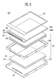
- FIG. 2 is an exploded schematic diagram perspective showing a liquid crystal display device according to a first exemplary embodiment of the present invention.
- FIG. 3 is a schematic diagram showing a flexible printed circuit board according to an exemplary embodiment of the present invention.
- FIGs. 4A and 4B are schematic cross-sectional diagrams showing a coupling between a liquid crystal display device and a flexible printed circuit board according to an exemplary embodiment of the present invention.
- FIG. 5 is a detailed diagram of a housing of FIGs. 4A and 4B .
- FIG. 6 is an exploded schematic diagram perspective showing a liquid crystal display device according to a second exemplary embodiment of the present invention.
- FIG. 2 is a perspective view showing a liquid crystal display device according to a first embodiment of the present invention.
- a liquid crystal display device 160 includes a liquid crystal display panel 104, a back light assembly 150, and a bottom chassis (or bezel) 122.
- the liquid crystal display panel 104 displays images and includes a first substrate 104a, a second substrate 104b, and liquid crystals injected between the first substrate 104a and the second substrate 104b.
- the second substrate 104b includes a plurality of thin film transistors (TFTs) arranged in a matrix.
- a source electrode of the TFT is coupled with a data line, and a gate electrode of the TFT is coupled with a scan line.
- a drain electrode of the TFT is coupled with a pixel electrode composed of a transparent conductive material.
- An integrated circuit 106 is located on one side of the second substrate 104b, and provides the data signal and the scan signal, and a periphery of the integrated circuit 106 is coated with a passivation layer 108.
- First pads 105 are located at one end of the second substrate 104b. The first pads 105 receive a drive signal (e.g., predetermined drive signal) from an external device and provide the drive signal to the integrated circuit 106.
- a drive signal e.g., predetermined drive signal
- the first substrate 104a faces the second substrate 104b.
- An entire surface of the first substrate 104a is coated with a common electrode composed of a transparent material.
- a suitable voltage e.g. a predetermined voltage
- an electric field is formed between the common electrode and the pixel electrode.
- the electric field changes alignment angle of a liquid crystal between the first substrate 104a and the second substrate 104b.
- Optical transmittance is changed to display desired images according to the changed alignment angle of the liquid crystal.
- the backlight assembly 150 includes a mold frame 116, a light guide plate 118, a reflection plate 120, and optical sheets 110.
- the light guide plate 118 provides light supplied from LEDs to the liquid crystal display panel 104.
- the LEDs are located on a side (e.g., an edge) of the light guide plate 118. Therefore, the light guide plate 118 provides light provided by the LEDs to its side toward the liquid crystal display panel 104.
- the reflection plate 120 is located at a rear surface of the light guide plate 118, and reflects incident light back toward the light guide plate 118, thereby improving the light efficiency.
- the optical sheets 110 improve the luminance of light supplied from the light guide plate 118 to the liquid crystal display panel 104.
- the mold frame 116 fixes and supports the backlight assembly 150 and the liquid crystal display panel 104.
- the mold frame 116 has sufficient strength (e.g., predetermined strength) to protect the backlight assembly 150 and the liquid crystal display panel 104 from external impact or shock.
- the bottom chassis 122 may be composed of aluminum and is fixed to enclose the mold frame 116.
- the bottom chassis 122 provides sufficient strength (e.g. predetermined strength) to the liquid crystal display device 160 to prevent or reduce the likelihood of distortion.
- At least one slit (or slit hole) 130 is located on one end of a bottom surface (i.e., the surface that is parallel to the light guide plate 118) of the bottom chassis 122.
- a fixture including an LED is inserted into the slit 130, and therefore, in one exemplary embodiment, the light guide plate 118 does not overlap the slit 130.
- FIG. 3 is a view showing a flexible printed circuit board (FPCB) according to an embodiment of the present invention.
- FPCB flexible printed circuit board
- second pads 202 and circuit components are located on the flexible printed circuit board (FPCB) 200 in an exemplary embodiment of the present invention.
- the second pads 202 are electrically coupled with the first pads 105 to supply a drive signal (e.g., a predetermined drive signal) to the first pads 105.
- a drive signal e.g., a predetermined drive signal
- the circuit components on the FPCB 200 generate a drive signal to be supplied to the second pads 202 and the housing 204.
- At least one housing 204 containing a light emitting diode is located on the FPCB 200.
- the housing 204 is electrically coupled to the FPCB 200 for receiving a drive signal provided from the FPCB 200 to an LED inside the housing 204.
- one side of the housing 204 is open to allow the transfer of light generated by the LED to the light guide plate 118.
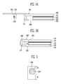
- FIG. 4A and FIG. 4B are cross-sectional views showing a coupling between the liquid crystal display device and a flexible printed circuit board according to the present invention.
- FIG. 5 is a detailed view showing the fixing portion shown in FIG. 4A and FIG. 4B .
- the first pads 105 and the second pads 202 are electrically coupled together.
- the FPCB 200 is bent at an angle (e.g., a predetermined angle) and attached to the rear surface of the bottom chassis 122 and configured such that the housing 204 is inserted in the slit (or through the slit) 130.
- the LED 206 is positioned adjacent an edge of the light guide plate 118. Accordingly, light generated by the light emitting diode 206 can be stably supplied to the light guide plate 118.
- a height h1 of a lower portion varies from a height h2 of an upper portion of the housing 204.
- the height h1 of the lower portion of the housing 204 in contact with the FPCB 200 is configured for the LED 206 to be positioned adjacent an edge of the light guide plate 118.
- the height h1 of the lower portion in the housing 204 is thicker than the height h2 of the upper portion in the housing 204 to take into account the bottom chassis 122 and to position the LED 204 at substantially a center of an edge of the light guide plate 118.
- a thickness of the bottom chassis 122 is configured to provide relatively high strength to the liquid crystal display device 160.
- the light emitting diode 206 may not be positioned at the center of an edge of the light guide plate 118, thereby deteriorating the efficiency of the light.
- the height h1 of the lower portion of the housing 204 is configured such that the light emitting diode 206 is positioned at substantially the center of an edge of the light guide plate 118, thereby improving the light efficiency.
- the housing 204 is configured such that the lower portion of the housing 204 is thicker than the upper portion of the housing 204.
- the housing 204 is directly attached to the FPCB 200, manufacturing cost can be reduced as compared with the conventional liquid crystal display device.
- the height h1 of a lower portion in the fixing portion 206 is set to be thicker than the height h2 of an upper portion therein, the light emitting diode 206 can be positioned at a central side of the light guide plate 118.
- FIG. 6 is a perspective view showing a liquid crystal display device according to a second embodiment of the present invention. Parts of FIG. 6 corresponding to those of FIG. 2 are designated by the same symbols and the description thereof is omitted.
- the liquid crystal display device further includes a top chassis 170.
- the top chassis 170 is fixed to the mold frame 116, and provides additional strength to a liquid crystal display device 160'.
- a single slit 131 is located at a bottom chassis 123. A length of the slit 131 allows housings 204 on an FPCB 200 to be insertable into the slit 131.
- the housing 204 is directly attached to the FPCB 200, manufacturing costs can be reduced as compared to a conventional liquid crystal display device incorporating a light emitting diode substrate. Additionally, because the height h1 of a lower portion of the housing 204 is greater than the height h2 of an upper portion thereof, the light emitting diode 206 can be positioned at substantially a center of an edge of the light guide plate 118.
Landscapes
- Physics & Mathematics (AREA)
- General Physics & Mathematics (AREA)
- Optics & Photonics (AREA)
- Nonlinear Science (AREA)
- Mathematical Physics (AREA)
- Chemical & Material Sciences (AREA)
- Crystallography & Structural Chemistry (AREA)
- Liquid Crystal (AREA)
- Devices For Indicating Variable Information By Combining Individual Elements (AREA)
Abstract
Description
- The present invention relates to a liquid crystal display device.
- Recently, various flat plate displays of relatively reduced weight and volume have been developed to overcome certain disadvantages of cathode ray tubes (CRTs). Exemplary flat panel displays include liquid crystal displays (LCDs), field emission displays (FEDs), plasma display panels (PDPs), and organic light emitting displays.
- Since liquid crystal display devices are relatively small, light weight, and have low power consumption, they have been targeted as substitutes for CRTs where applicable. Liquid crystal display devices have been used on relatively large products such as monitors and TVs as well as on portable devices such as portable phones and Personal Digital Assistants (PDAs).
- Liquid crystal display devices applied to portable devices use at least one light emitting diode (LED) as a light source to express an image of a certain luminance. As shown in
FIG. 1A , a conventional liquid crystal display device includes a lightemitting diode substrate 2 and at least onehousing 4 on the lightemitting diode substrate 2. The lightemitting diode substrate 2 is fixedly attached within a mold frame and supplies a control signal from a flexible printed circuit board (FPCB) to thehousing 4. Thehousing 4 is attached to and electrically coupled to the lightemitting diode substrate 2. As shown inFIG. 1B , thehousing 4 includes anLED 6 fixed therein for generating light corresponding to a control signal provided from thehousing 4. Including a lightemitting diode substrate 2 in a conventional liquid crystal display panel results in an increase of manufacturing cost. - According to aspects of the present invention, a liquid crystal display device is provided that reduces manufacturing cost.
- In an exemplary embodiment of the present invention, a liquid crystal display device is provided including a liquid crystal display panel for displaying images, the liquid crystal display panel having a first pad located on a first peripheral portion of the liquid crystal display panel, a light guide plate for providing light supplied to an edge of the light guide plate to the liquid crystal display panel, and a bottom chassis having at least one slit formed thereon, the light guide plate being located between the liquid crystal display panel and the bottom chassis. A flexible printed circuit board is located at the first peripheral portion of the liquid crystal display panel and includes a second pad coupled to the first pad. At least one housing is located on the flexible printed circuit board, the at least one housing supporting a light emitting diode supplying light to the light guide plate, wherein the light emitting diode is positioned at the edge of the light guide plate through the at least one slit. The housing includes a first portion and a second portion on opposite sides of the light emitting diode, the thickness of the first portion being different from that of the second portion, and wherein the first portion is adjacent to the flexible printed circuit board.
- In one exemplary embodiment, the thickness of the first portion of the housing is greater than the thickness of the second portion of the housing. The thickness of the first portion and the thickness of the second portion of the housing are configured to position the light emitting diode at substantially a center of an edge of the light guide plate. Further, the light guide plate may be configured not to overlap the at least one slit.
- In one exemplary embodiment, the flexible printed circuit board includes at least two housings, each housing within a separate slit. In another exemplary embodiment, each housing is within a single slit. Further, the at least one housing may be directly attached to the flexible printed circuit board.
- In yet another exemplary embodiment, a light emitting diode housing is provided for a liquid crystal display device as described above. The light emitting diode housing includes a groove for containing a light emitting diode, an upper portion on a first side of the groove having a first thickness, and a lower portion on a second opposite side of the groove having a second thickness wherein the second thickness varies the first thickness, wherein the housing is attachable to the flexible printed circuit board.
Preferably, the second thickness is greater than the first thickness. Preferably, the housing is adapted to position the groove substantially at a center of an edge in a thickness direction of the light guide plate. Preferably, the housing is adapted to be inserted through the at least one slit. - The accompanying drawings, together with the specification, illustrate exemplary embodiments of the present invention, and, together with the description, serve to explain the principles of the present invention.
-
FIG. 1A and FIG. 1B are schematics showing a conventional light emitting diode substrate and housing. -
FIG. 2 is an exploded schematic diagram perspective showing a liquid crystal display device according to a first exemplary embodiment of the present invention. -
FIG. 3 is a schematic diagram showing a flexible printed circuit board according to an exemplary embodiment of the present invention. -
FIGs. 4A and 4B are schematic cross-sectional diagrams showing a coupling between a liquid crystal display device and a flexible printed circuit board according to an exemplary embodiment of the present invention. -
FIG. 5 is a detailed diagram of a housing ofFIGs. 4A and 4B . -
FIG. 6 is an exploded schematic diagram perspective showing a liquid crystal display device according to a second exemplary embodiment of the present invention. - In the following detailed description, only certain exemplary embodiments of the present invention are shown and described, by way of illustration. Here, when a first element is described as being connected to a second element, the first element may be directly connected to the second element or may be indirectly connected to the second element via a third element. Further, some of the elements that are not essential to the complete understanding of the invention are omitted for clarity. As those skilled in the art will recognize, the invention may be embodied in many different forms and should not be construed as being limited to the embodiments set forth herein. Like reference numerals designate like elements throughout the specification.
-
FIG. 2 is a perspective view showing a liquid crystal display device according to a first embodiment of the present invention. - With reference to
FIG. 2 , a liquidcrystal display device 160 according to a first exemplary embodiment of the present invention includes a liquidcrystal display panel 104, aback light assembly 150, and a bottom chassis (or bezel) 122. The liquidcrystal display panel 104 displays images and includes afirst substrate 104a, asecond substrate 104b, and liquid crystals injected between thefirst substrate 104a and thesecond substrate 104b. - The
second substrate 104b includes a plurality of thin film transistors (TFTs) arranged in a matrix. A source electrode of the TFT is coupled with a data line, and a gate electrode of the TFT is coupled with a scan line. A drain electrode of the TFT is coupled with a pixel electrode composed of a transparent conductive material. When a scan signal is supplied to the scan line, the TFT is turned on to provide a data signal supplied to the data line to the pixel electrode. - An
integrated circuit 106 is located on one side of thesecond substrate 104b, and provides the data signal and the scan signal, and a periphery of the integratedcircuit 106 is coated with apassivation layer 108.First pads 105 are located at one end of thesecond substrate 104b. Thefirst pads 105 receive a drive signal (e.g., predetermined drive signal) from an external device and provide the drive signal to the integratedcircuit 106. - The
first substrate 104a faces thesecond substrate 104b. An entire surface of thefirst substrate 104a is coated with a common electrode composed of a transparent material. When a suitable voltage (e.g. a predetermined voltage) is applied to the common electrode, an electric field is formed between the common electrode and the pixel electrode. The electric field changes alignment angle of a liquid crystal between thefirst substrate 104a and thesecond substrate 104b. Optical transmittance is changed to display desired images according to the changed alignment angle of the liquid crystal. - The
backlight assembly 150 includes amold frame 116, alight guide plate 118, areflection plate 120, andoptical sheets 110. Thelight guide plate 118 provides light supplied from LEDs to the liquidcrystal display panel 104. Here, the LEDs are located on a side (e.g., an edge) of thelight guide plate 118. Therefore, thelight guide plate 118 provides light provided by the LEDs to its side toward the liquidcrystal display panel 104. - The
reflection plate 120 is located at a rear surface of thelight guide plate 118, and reflects incident light back toward thelight guide plate 118, thereby improving the light efficiency. Theoptical sheets 110 improve the luminance of light supplied from thelight guide plate 118 to the liquidcrystal display panel 104. Themold frame 116 fixes and supports thebacklight assembly 150 and the liquidcrystal display panel 104. Themold frame 116 has sufficient strength (e.g., predetermined strength) to protect thebacklight assembly 150 and the liquidcrystal display panel 104 from external impact or shock. - The
bottom chassis 122 may be composed of aluminum and is fixed to enclose themold frame 116. Thebottom chassis 122 provides sufficient strength (e.g. predetermined strength) to the liquidcrystal display device 160 to prevent or reduce the likelihood of distortion. - At least one slit (or slit hole) 130 is located on one end of a bottom surface (i.e., the surface that is parallel to the light guide plate 118) of the
bottom chassis 122. A fixture including an LED is inserted into theslit 130, and therefore, in one exemplary embodiment, thelight guide plate 118 does not overlap theslit 130. -
FIG. 3 is a view showing a flexible printed circuit board (FPCB) according to an embodiment of the present invention. - Referring to
FIG. 3 ,second pads 202 and circuit components are located on the flexible printed circuit board (FPCB) 200 in an exemplary embodiment of the present invention. Thesecond pads 202 are electrically coupled with thefirst pads 105 to supply a drive signal (e.g., a predetermined drive signal) to thefirst pads 105. More specifically, the circuit components on theFPCB 200 generate a drive signal to be supplied to thesecond pads 202 and thehousing 204. - At least one
housing 204 containing a light emitting diode is located on theFPCB 200. Thehousing 204 is electrically coupled to theFPCB 200 for receiving a drive signal provided from theFPCB 200 to an LED inside thehousing 204. In one exemplary embodiment, one side of thehousing 204 is open to allow the transfer of light generated by the LED to thelight guide plate 118. -
FIG. 4A and FIG. 4B are cross-sectional views showing a coupling between the liquid crystal display device and a flexible printed circuit board according to the present invention.FIG. 5 is a detailed view showing the fixing portion shown inFIG. 4A and FIG. 4B . - With reference to
FIGs. 4A and 4B , thefirst pads 105 and thesecond pads 202 are electrically coupled together. TheFPCB 200 is bent at an angle (e.g., a predetermined angle) and attached to the rear surface of thebottom chassis 122 and configured such that thehousing 204 is inserted in the slit (or through the slit) 130. As such, theLED 206 is positioned adjacent an edge of thelight guide plate 118. Accordingly, light generated by thelight emitting diode 206 can be stably supplied to thelight guide plate 118. - As shown in
FIG. 5 , a height h1 of a lower portion varies from a height h2 of an upper portion of thehousing 204. For example, the height h1 of the lower portion of thehousing 204 in contact with theFPCB 200 is configured for theLED 206 to be positioned adjacent an edge of thelight guide plate 118. In one exemplary embodiment, the height h1 of the lower portion in thehousing 204 is thicker than the height h2 of the upper portion in thehousing 204 to take into account thebottom chassis 122 and to position theLED 204 at substantially a center of an edge of thelight guide plate 118. - A thickness of the
bottom chassis 122 is configured to provide relatively high strength to the liquidcrystal display device 160. When the height h1 of a lower portion and the height h2 of an upper portion in thehousing 204 are identical, thelight emitting diode 206 may not be positioned at the center of an edge of thelight guide plate 118, thereby deteriorating the efficiency of the light. Accordingly, the height h1 of the lower portion of thehousing 204 is configured such that thelight emitting diode 206 is positioned at substantially the center of an edge of thelight guide plate 118, thereby improving the light efficiency. In other words, in accordance with aspects of the present invention, thehousing 204 is configured such that the lower portion of thehousing 204 is thicker than the upper portion of thehousing 204. - As described earlier, in the present invention, since the
housing 204 is directly attached to theFPCB 200, manufacturing cost can be reduced as compared with the conventional liquid crystal display device. In addition, in the present invention, because the height h1 of a lower portion in the fixingportion 206 is set to be thicker than the height h2 of an upper portion therein, thelight emitting diode 206 can be positioned at a central side of thelight guide plate 118. -
FIG. 6 is a perspective view showing a liquid crystal display device according to a second embodiment of the present invention. Parts ofFIG. 6 corresponding to those ofFIG. 2 are designated by the same symbols and the description thereof is omitted. - With reference to
FIG. 6 , the liquid crystal display device according to a second exemplary embodiment of the present invention further includes atop chassis 170. Thetop chassis 170 is fixed to themold frame 116, and provides additional strength to a liquid crystal display device 160'. Furthermore, asingle slit 131 is located at abottom chassis 123. A length of theslit 131 allowshousings 204 on anFPCB 200 to be insertable into theslit 131. - As described earlier, since the
housing 204 is directly attached to theFPCB 200, manufacturing costs can be reduced as compared to a conventional liquid crystal display device incorporating a light emitting diode substrate. Additionally, because the height h1 of a lower portion of thehousing 204 is greater than the height h2 of an upper portion thereof, thelight emitting diode 206 can be positioned at substantially a center of an edge of thelight guide plate 118. - While the present invention has been described in connection with certain exemplary embodiments, it is to be understood that the invention is not limited to the disclosed embodiments, but, on the contrary, is intended to cover various modifications and equivalent arrangements included within the scope of the appended claims, and equivalents thereof.
Claims (10)
- A liquid crystal display device comprising:a liquid crystal display panel (104) for displaying images, the liquid crystal display panel (104) comprising at least a first pad (105) located at a first peripheral portion of the liquid crystal display panel (104);a light guide plate (118) for providing light supplied to a lateral edge of the light guide plate (118) to the liquid crystal display panel (104);a bottom chassis (122, 123) having at least one slit (130, 131) thereon, the light guide plate (118) being located between the liquid crystal display panel and the bottom chassis (122, 123);a flexible printed circuit board (200) fixed at the first peripheral portion of the liquid crystal display panel (104) and comprising at least a second pad (202) coupled to the at least one first pad (105);at least one housing (204) on the flexible printed circuit board (200), the at least one housing (204) supporting a light emitting diode (206) for supplying light to the light guide plate (118), wherein the light emitting diode (206) is positioned at the lateral edge of the light guide plate (118) through the at least one slit (130, 131); andwherein the housing (204) comprises a first portion and a second portion on opposite sides of the light emitting diode (206), the thickness (h1) of the first portion being different from the thickness (h2) of the second portion, and wherein the first portion is adjacent to the flexible printed circuit board (200).
- The liquid crystal display device as claimed in claim 1, wherein the thickness (h1) of the first portion of the housing (204) is greater than the thickness (h2) of the second portion of the housing (204).
- The liquid crystal display device as claimed in one of the preceding claims, wherein the thickness (h2) of the second portion and the thickness (h1) of the first portion of the housing are configured to position the light emitting diode (206) at substantially a center of the lateral edge in a thickness direction of the light guide plate (118).
- The liquid crystal display device as claimed in one of the preceding claims, wherein the light guide plate (118) does not overlap the at least one slit (130, 131).
- The liquid crystal display device as claimed in one of the preceding claims, wherein the flexible printed circuit board (200) has at least two housings (204) thereon, each housing being inserted through a separate one of at least two slits (130).
- The liquid crystal display device as claimed in one of claims 1-4, wherein the flexible printed circuit board (200) has at least two housings (204) thereon, wherein the at least two housings (204) are inserted through a single slit (131).
- The liquid crystal display device as claimed in one of the preceding claims, further comprising:a reflection plate (120) between the bottom chassis (122, 123) and the light guide plate (118);optical sheets (110) between the light guide plate (118) and the liquid crystal display panel (104); anda mold frame (116) for fixing the light guide plate (118), the reflection plate (120), and the optical sheets (110).
- The liquid crystal display device as claimed in claim 7, further comprising a top chassis (170) on the liquid crystal display panel (104) and coupled to the mold frame (116).
- The liquid crystal display device as claimed in one of the preceding claims, wherein the at least one housing (204) is directly attached to the flexible printed circuit board (200).
- The liquid crystal display device as claimed in one of the preceding claims, wherein the at least one housing (204) comprises a groove for containing a light emitting diode (206).
Applications Claiming Priority (1)
| Application Number | Priority Date | Filing Date | Title |
|---|---|---|---|
| KR1020070045556A KR100857693B1 (en) | 2007-05-10 | 2007-05-10 | Liquid crystal display |
Publications (1)
| Publication Number | Publication Date |
|---|---|
| EP1990663A1 true EP1990663A1 (en) | 2008-11-12 |
Family
ID=39587607
Family Applications (1)
| Application Number | Title | Priority Date | Filing Date |
|---|---|---|---|
| EP08155946A Withdrawn EP1990663A1 (en) | 2007-05-10 | 2008-05-09 | Liquid crystal display device |
Country Status (5)
| Country | Link |
|---|---|
| US (1) | US7777829B2 (en) |
| EP (1) | EP1990663A1 (en) |
| JP (1) | JP2008281981A (en) |
| KR (1) | KR100857693B1 (en) |
| CN (1) | CN101303482B (en) |
Families Citing this family (13)
| Publication number | Priority date | Publication date | Assignee | Title |
|---|---|---|---|---|
| TWI366018B (en) * | 2008-03-21 | 2012-06-11 | Au Optronics Corp | Backlight module with integrated base and method of manufacturing thereof |
| KR101321271B1 (en) * | 2008-11-18 | 2013-10-25 | 엘지디스플레이 주식회사 | Liquid crystal display device |
| KR101693655B1 (en) | 2009-11-12 | 2017-01-06 | 엘지전자 주식회사 | Back Light Unit And Liquid Crystal Display Device Comprising Thereof |
| USRE46781E1 (en) | 2009-11-12 | 2018-04-10 | Lg Electronics Inc. | Backlight unit and liquid crystal display including the same |
| KR20110103074A (en) | 2010-03-12 | 2011-09-20 | 엘지전자 주식회사 | Display device |
| JP2012032763A (en) * | 2010-06-28 | 2012-02-16 | Hitachi Consumer Electronics Co Ltd | Liquid crystal display device, backlight, and led |
| BR112012032082B1 (en) * | 2010-06-30 | 2019-11-26 | Avon Products, Inc. | COSMETIC COMPOSITION AND METHOD TO IMPROVE AESTHETIC APPEARANCE OF HUMAN SKIN |
| KR101147417B1 (en) * | 2010-07-08 | 2012-05-23 | 삼성모바일디스플레이주식회사 | Liquid crystal display and fabricating method of the same |
| TWI440927B (en) * | 2011-01-18 | 2014-06-11 | 瀚宇彩晶股份有限公司 | Display device and backlight module thereof |
| CN102636908A (en) * | 2011-02-15 | 2012-08-15 | 瀚宇彩晶股份有限公司 | Display device and backlight module thereof |
| KR102090462B1 (en) | 2013-08-30 | 2020-03-18 | 엘지디스플레이 주식회사 | liquid crystal display display |
| KR102148718B1 (en) * | 2013-12-18 | 2020-08-27 | 삼성전자주식회사 | Display device |
| TWI835508B (en) * | 2023-01-05 | 2024-03-11 | 友達光電股份有限公司 | Display device |
Citations (4)
| Publication number | Priority date | Publication date | Assignee | Title |
|---|---|---|---|---|
| US20040037063A1 (en) * | 2002-08-26 | 2004-02-26 | Minebea Co., Ltd., Kitasaku-Gun, Japan | Spread illuminating apparatus with housing frame |
| US20060092665A1 (en) * | 2004-11-02 | 2006-05-04 | Samsung Electro-Mechanics Co., Ltd. | Light emitting diode and backlight apparatus having the same |
| US20060291240A1 (en) * | 2005-06-13 | 2006-12-28 | Jae-Kwang Kim | Backlight assembly, display device having the same, and method thereof |
| US20070091242A1 (en) * | 2005-10-20 | 2007-04-26 | Hitachi Displays, Ltd. | Liquid crystal display device |
Family Cites Families (17)
| Publication number | Priority date | Publication date | Assignee | Title |
|---|---|---|---|---|
| JP3642263B2 (en) | 2000-05-23 | 2005-04-27 | セイコーエプソン株式会社 | Liquid crystal device and electronic device |
| JP4226796B2 (en) | 2001-05-30 | 2009-02-18 | 株式会社日立製作所 | Liquid crystal display |
| JP4045781B2 (en) * | 2001-08-28 | 2008-02-13 | 松下電工株式会社 | Light emitting device |
| JP2003156739A (en) * | 2001-11-21 | 2003-05-30 | Kawaguchiko Seimitsu Co Ltd | Liquid crystal display device |
| JP2003344851A (en) | 2002-05-22 | 2003-12-03 | Optrex Corp | Liquid crystal display device |
| JP4345337B2 (en) * | 2003-03-31 | 2009-10-14 | セイコーエプソン株式会社 | Electro-optical device and electronic apparatus |
| KR100989338B1 (en) * | 2003-07-01 | 2010-10-25 | 삼성전자주식회사 | Back light assembly and liquid crystal display device having same |
| JP2005135860A (en) | 2003-10-31 | 2005-05-26 | Harison Toshiba Lighting Corp | LED backlight device |
| JP4525065B2 (en) * | 2003-12-11 | 2010-08-18 | セイコーエプソン株式会社 | Electro-optical device, manufacturing method thereof, and electronic apparatus |
| JP2005283829A (en) * | 2004-03-29 | 2005-10-13 | Seiko Epson Corp | Electro-optical device and electronic apparatus |
| JP2005326454A (en) | 2004-05-12 | 2005-11-24 | Optrex Corp | Display device |
| JP4055741B2 (en) | 2004-05-24 | 2008-03-05 | セイコーエプソン株式会社 | Electro-optical device and electronic apparatus |
| US7284894B2 (en) * | 2005-05-31 | 2007-10-23 | Avago Technologies Eceliip (Singapore) Pte Ltd | Light source utilizing a flexible circuit carrier |
| KR20060132202A (en) * | 2005-06-17 | 2006-12-21 | 삼성전자주식회사 | LCD Display |
| KR20070065079A (en) * | 2005-12-19 | 2007-06-22 | 삼성전자주식회사 | LED lamp unit, backlight assembly including the same, and display device having same |
| TWM309757U (en) * | 2006-09-19 | 2007-04-11 | Everlight Electronics Co Ltd | Side view LED package structure |
| TW200905311A (en) * | 2007-07-31 | 2009-02-01 | Chi Mei Lighting Tech Corp | Backlight module and application thereof |
-
2007
- 2007-05-10 KR KR1020070045556A patent/KR100857693B1/en not_active Expired - Fee Related
- 2007-09-18 JP JP2007240968A patent/JP2008281981A/en active Pending
-
2008
- 2008-03-27 US US12/057,231 patent/US7777829B2/en not_active Expired - Fee Related
- 2008-05-09 EP EP08155946A patent/EP1990663A1/en not_active Withdrawn
- 2008-05-12 CN CN2008100970375A patent/CN101303482B/en not_active Expired - Fee Related
Patent Citations (4)
| Publication number | Priority date | Publication date | Assignee | Title |
|---|---|---|---|---|
| US20040037063A1 (en) * | 2002-08-26 | 2004-02-26 | Minebea Co., Ltd., Kitasaku-Gun, Japan | Spread illuminating apparatus with housing frame |
| US20060092665A1 (en) * | 2004-11-02 | 2006-05-04 | Samsung Electro-Mechanics Co., Ltd. | Light emitting diode and backlight apparatus having the same |
| US20060291240A1 (en) * | 2005-06-13 | 2006-12-28 | Jae-Kwang Kim | Backlight assembly, display device having the same, and method thereof |
| US20070091242A1 (en) * | 2005-10-20 | 2007-04-26 | Hitachi Displays, Ltd. | Liquid crystal display device |
Also Published As
| Publication number | Publication date |
|---|---|
| CN101303482B (en) | 2010-09-29 |
| JP2008281981A (en) | 2008-11-20 |
| US7777829B2 (en) | 2010-08-17 |
| US20080278653A1 (en) | 2008-11-13 |
| KR100857693B1 (en) | 2008-09-08 |
| CN101303482A (en) | 2008-11-12 |
Similar Documents
| Publication | Publication Date | Title |
|---|---|---|
| US7777829B2 (en) | Liquid crystal display device | |
| EP1956401B1 (en) | Display device with a bottom chassis | |
| KR100711872B1 (en) | Portable display | |
| CN101226294A (en) | Display unit with bottom bracket | |
| JP4391493B2 (en) | Portable display device | |
| US8031291B2 (en) | Liquid crystal display and tablet computer having a chassis fastening member that receives a printed circuit board | |
| KR100719658B1 (en) | Portable display | |
| KR100947429B1 (en) | LCD Display | |
| KR100759675B1 (en) | Portable display | |
| KR100873701B1 (en) | Liquid crystal display | |
| KR100759673B1 (en) | Portable display | |
| US7656494B2 (en) | Display device | |
| KR20060090392A (en) | Flat panel display for EMI shielding | |
| KR100745351B1 (en) | Portable display device | |
| KR100793533B1 (en) | Portable display | |
| KR100793541B1 (en) | Portable display | |
| KR100759694B1 (en) | Portable display | |
| KR20060081588A (en) | Backlight assembly with improved adhesion and flat panel display device having same | |
| KR100852346B1 (en) | Liquid crystal display | |
| KR100786472B1 (en) | Flat Panel Display and Manufacturing Method | |
| KR100754132B1 (en) | Portable display | |
| KR100784043B1 (en) | Flat Panel Display | |
| KR20080054503A (en) | Liquid crystal display | |
| KR20070121478A (en) | Portable display | |
| KR20060078867A (en) | Flat panel display device to prevent electrostatic discharge |
Legal Events
| Date | Code | Title | Description |
|---|---|---|---|
| PUAI | Public reference made under article 153(3) epc to a published international application that has entered the european phase |
Free format text: ORIGINAL CODE: 0009012 |
|
| 17P | Request for examination filed |
Effective date: 20080509 |
|
| AK | Designated contracting states |
Kind code of ref document: A1 Designated state(s): AT BE BG CH CY CZ DE DK EE ES FI FR GB GR HR HU IE IS IT LI LT LU LV MC MT NL NO PL PT RO SE SI SK TR |
|
| AX | Request for extension of the european patent |
Extension state: AL BA MK RS |
|
| RIN1 | Information on inventor provided before grant (corrected) |
Inventor name: JANG, JIN-SEOK,SAMSUNG SDI CO., LTD. Inventor name: SUNG, JIN-HEE,L Inventor name: CHUNG, JAE-MO,SAMSUNG SDI CO., LTD. |
|
| RAP1 | Party data changed (applicant data changed or rights of an application transferred) |
Owner name: SAMSUNG MOBILE DISPLAY CO., LTD. |
|
| AKX | Designation fees paid |
Designated state(s): DE FR GB |
|
| 17Q | First examination report despatched |
Effective date: 20100709 |
|
| RAP1 | Party data changed (applicant data changed or rights of an application transferred) |
Owner name: SAMSUNG DISPLAY CO., LTD. |
|
| STAA | Information on the status of an ep patent application or granted ep patent |
Free format text: STATUS: THE APPLICATION IS DEEMED TO BE WITHDRAWN |
|
| 18D | Application deemed to be withdrawn |
Effective date: 20140128 |