EP1986479A2 - Wiring substrate and current detection device - Google Patents
Wiring substrate and current detection device Download PDFInfo
- Publication number
- EP1986479A2 EP1986479A2 EP08153463A EP08153463A EP1986479A2 EP 1986479 A2 EP1986479 A2 EP 1986479A2 EP 08153463 A EP08153463 A EP 08153463A EP 08153463 A EP08153463 A EP 08153463A EP 1986479 A2 EP1986479 A2 EP 1986479A2
- Authority
- EP
- European Patent Office
- Prior art keywords
- land
- wiring pattern
- wiring
- shunt resistor
- central line
- Prior art date
- Legal status (The legal status is an assumption and is not a legal conclusion. Google has not performed a legal analysis and makes no representation as to the accuracy of the status listed.)
- Granted
Links
Images


Classifications
-
- H—ELECTRICITY
- H05—ELECTRIC TECHNIQUES NOT OTHERWISE PROVIDED FOR
- H05K—PRINTED CIRCUITS; CASINGS OR CONSTRUCTIONAL DETAILS OF ELECTRIC APPARATUS; MANUFACTURE OF ASSEMBLAGES OF ELECTRICAL COMPONENTS
- H05K3/00—Apparatus or processes for manufacturing printed circuits
- H05K3/30—Assembling printed circuits with electric components, e.g. with resistors
- H05K3/32—Assembling printed circuits with electric components, e.g. with resistors electrically connecting electric components or wires to printed circuits
- H05K3/34—Assembling printed circuits with electric components, e.g. with resistors electrically connecting electric components or wires to printed circuits by soldering
- H05K3/341—Surface mounted components
- H05K3/3421—Leaded components
-
- G—PHYSICS
- G01—MEASURING; TESTING
- G01R—MEASURING ELECTRIC VARIABLES; MEASURING MAGNETIC VARIABLES
- G01R1/00—Details of instruments or arrangements of the types included in groups G01R5/00 - G01R13/00 and G01R31/00
- G01R1/20—Modifications of basic electric elements for use in electric measuring instruments; Structural combinations of such elements with such instruments
- G01R1/203—Resistors used for electric measuring, e.g. decade resistors standards, resistors for comparators, series resistors, shunts
-
- H—ELECTRICITY
- H05—ELECTRIC TECHNIQUES NOT OTHERWISE PROVIDED FOR
- H05K—PRINTED CIRCUITS; CASINGS OR CONSTRUCTIONAL DETAILS OF ELECTRIC APPARATUS; MANUFACTURE OF ASSEMBLAGES OF ELECTRICAL COMPONENTS
- H05K1/00—Printed circuits
- H05K1/02—Details
- H05K1/11—Printed elements for providing electric connections to or between printed circuits
- H05K1/111—Pads for surface mounting, e.g. lay-out
-
- H—ELECTRICITY
- H05—ELECTRIC TECHNIQUES NOT OTHERWISE PROVIDED FOR
- H05K—PRINTED CIRCUITS; CASINGS OR CONSTRUCTIONAL DETAILS OF ELECTRIC APPARATUS; MANUFACTURE OF ASSEMBLAGES OF ELECTRICAL COMPONENTS
- H05K2201/00—Indexing scheme relating to printed circuits covered by H05K1/00
- H05K2201/09—Shape and layout
- H05K2201/09209—Shape and layout details of conductors
- H05K2201/09218—Conductive traces
- H05K2201/09281—Layout details of a single conductor
-
- H—ELECTRICITY
- H05—ELECTRIC TECHNIQUES NOT OTHERWISE PROVIDED FOR
- H05K—PRINTED CIRCUITS; CASINGS OR CONSTRUCTIONAL DETAILS OF ELECTRIC APPARATUS; MANUFACTURE OF ASSEMBLAGES OF ELECTRICAL COMPONENTS
- H05K2201/00—Indexing scheme relating to printed circuits covered by H05K1/00
- H05K2201/09—Shape and layout
- H05K2201/09209—Shape and layout details of conductors
- H05K2201/09372—Pads and lands
- H05K2201/09381—Shape of non-curved single flat metallic pad, land or exposed part thereof; Shape of electrode of leadless component
-
- H—ELECTRICITY
- H05—ELECTRIC TECHNIQUES NOT OTHERWISE PROVIDED FOR
- H05K—PRINTED CIRCUITS; CASINGS OR CONSTRUCTIONAL DETAILS OF ELECTRIC APPARATUS; MANUFACTURE OF ASSEMBLAGES OF ELECTRICAL COMPONENTS
- H05K2201/00—Indexing scheme relating to printed circuits covered by H05K1/00
- H05K2201/09—Shape and layout
- H05K2201/09818—Shape or layout details not covered by a single group of H05K2201/09009 - H05K2201/09809
- H05K2201/09909—Special local insulating pattern, e.g. as dam around component
-
- H—ELECTRICITY
- H05—ELECTRIC TECHNIQUES NOT OTHERWISE PROVIDED FOR
- H05K—PRINTED CIRCUITS; CASINGS OR CONSTRUCTIONAL DETAILS OF ELECTRIC APPARATUS; MANUFACTURE OF ASSEMBLAGES OF ELECTRICAL COMPONENTS
- H05K2203/00—Indexing scheme relating to apparatus or processes for manufacturing printed circuits covered by H05K3/00
- H05K2203/04—Soldering or other types of metallurgic bonding
- H05K2203/0465—Shape of solder, e.g. differing from spherical shape, different shapes due to different solder pads
-
- H—ELECTRICITY
- H05—ELECTRIC TECHNIQUES NOT OTHERWISE PROVIDED FOR
- H05K—PRINTED CIRCUITS; CASINGS OR CONSTRUCTIONAL DETAILS OF ELECTRIC APPARATUS; MANUFACTURE OF ASSEMBLAGES OF ELECTRICAL COMPONENTS
- H05K2203/00—Indexing scheme relating to apparatus or processes for manufacturing printed circuits covered by H05K3/00
- H05K2203/16—Inspection; Monitoring; Aligning
- H05K2203/167—Using mechanical means for positioning, alignment or registration, e.g. using rod-in-hole alignment
-
- H—ELECTRICITY
- H05—ELECTRIC TECHNIQUES NOT OTHERWISE PROVIDED FOR
- H05K—PRINTED CIRCUITS; CASINGS OR CONSTRUCTIONAL DETAILS OF ELECTRIC APPARATUS; MANUFACTURE OF ASSEMBLAGES OF ELECTRICAL COMPONENTS
- H05K3/00—Apparatus or processes for manufacturing printed circuits
- H05K3/22—Secondary treatment of printed circuits
- H05K3/222—Completing of printed circuits by adding non-printed jumper connections
-
- Y—GENERAL TAGGING OF NEW TECHNOLOGICAL DEVELOPMENTS; GENERAL TAGGING OF CROSS-SECTIONAL TECHNOLOGIES SPANNING OVER SEVERAL SECTIONS OF THE IPC; TECHNICAL SUBJECTS COVERED BY FORMER USPC CROSS-REFERENCE ART COLLECTIONS [XRACs] AND DIGESTS
- Y02—TECHNOLOGIES OR APPLICATIONS FOR MITIGATION OR ADAPTATION AGAINST CLIMATE CHANGE
- Y02P—CLIMATE CHANGE MITIGATION TECHNOLOGIES IN THE PRODUCTION OR PROCESSING OF GOODS
- Y02P70/00—Climate change mitigation technologies in the production process for final industrial or consumer products
- Y02P70/50—Manufacturing or production processes characterised by the final manufactured product
Definitions
- the present invention relates to a wiring substrate mounted with a shunt resistor for current detection of an electronic circuit, and a current detection device equipped with the wiring substrate.
- a shunt resistor is incorporated in the middle of a line through which the current of the electronic circuit flows, and the current is detected based on the voltage drop by the shunt resistor.
- two lands for soldering both ends of the shunt resistor and voltage measurement wiring patterns pulled out from one end in a direction perpendicular to the direction a current to be detected of each land flows are arranged on a substrate, where the voltage difference among the terminals of each of the wiring patterns is detected by a current detection circuit, and the current to be detected is calculated from the voltage difference and a current conversion graph.
- the current detection circuit includes those described in Japanese Patent Application Laid-Open No.
- Japanese Patent Application Laid-Open No. 2003-121478 Japanese Patent Application Laid-Open No. 2003-121478 , and Japanese Patent Application Laid-Open No. 2003-121481 .
- the current detection circuits of Japanese Patent Application Laid-Open No. 2003-121478 and Japanese Patent Application Laid-Open No. 2003-121481 are contrived in an aim of enhancing the detection accuracy of the current to be detected.
- a wiring pattern for detecting the potential difference between both ends of the shunt resistor is pulled out from a location at where the current to be detected of each land mounted with both ends of the shunt resistor barely flows, or from an outer edge of each land positioned on an extended line of a wiring pattern for flowing the current to be detected connected to each land in order to enhance the detection accuracy of the current to be detected.
- Japanese Patent Application Laid-Open No. 2002-372551 Japanese Patent Application Laid-Open No. 2002-372550 , Japanese Patent Application Laid-Open No. 2003-121477 , Japanese Patent Application Laid-Open No. 2003-121478 , and Japanese Patent Application Laid-Open No.
- the wiring patterns for detecting the potential different of both ends of the shunt resistor are pulled out in a direction of approaching each other from the opposing outer edges of each land mounted with both ends of the shunt resistor, and thereafter, bent at right angles and pulled towards the side.
- both ends of the shunt resistor are soldered to the land of the substrate, but if cracks form in the solder between the shunt resistor and the wiring pattern, the wiring path for detecting the current to be detected changes and the resistance value of the wiring path changes, whereby the potential difference in the shunt resistor and the current to be detected cannot be accurately detected.
- the area of the land is only slightly larger than the area of the surface of the shunt resistor contacting the land as in Japanese Patent Application Laid-Open No. 2002-5968 , Japanese Patent Application Laid-Open No. 2002-372551 , and Japanese Patent Application Laid-Open No. 2002-372550 , the solder fillet formed from the shunt resistor to the land is small, the soldering strength is low, and soldering cracks are likely to form.
- the present invention relates to a wiring substrate including a land mounted with each rectangular surface of a shunt resistor, which has the rectangular surface at each of both ends thereof and has a central part floating with respect to the rectangular surfaces, and a wiring pattern for detecting a potential difference between the both ends of the shunt resistor pulled out from the land; and a current connection device including the shunt resistor, the wiring substrate, and a current detection circuit for detecting the potential difference between the both ends of the shunt resistor through the wiring pattern and detecting a current flowing to an electronic circuit formed on the wiring substrate based on the potential difference, respectively having the following configuration.
- the land is configured by a first land and a second land each having a rectangular portion and being arranged at a predetermined interval with a virtual central line as a center, a third land having an area smaller than that of the first land and being arranged at one end of a direction parallel to the central line of the first land to be connected to the first land, and a fourth land having an area smaller than that of the second land and being arranged at one end of a direction parallel to the central line of the second land to be connected to the second land.
- the wiring pattern is configured by a first wiring pattern connected to the third land and pulled out from the third land towards the fourth land, a second wiring pattern connected to the fourth land and pulled out from the fourth land towards the third land, a third wiring pattern connected to the first wiring pattern and pulled out in one direction parallel to the central line, and a fourth wiring connected to the second wiring pattern and pulled out in one direction parallel to the central line.
- each of the rectangular surfaces of the shunt resistor is mounted on and soldered to the first land and the second land each having a large area, and the solder fillet formed from the shunt resistor to the first land and the second land is enlarged, thereby increasing the solder strength.
- cracks are less likely to be formed in the solder between the shunt resistor and the wiring pattern, the wiring path for detecting the current to be detected and the resistance value of the wiring path do not change, and the potential difference between the both ends of the shunt resistor and the current to be detected flowing through the electronic circuit can be accurately detected.
- the wiring path for detecting the current to be detected that is, the wiring patterns can be separated from the wiring path through which the current to be detected flows, that is, the path from the land on one side of the central line to the land on the other side through the shunt resistor.
- the current to be detected does not flow into the wiring patterns, and the current to be detected can be accurately detected based on the potential difference between the both ends of the shunt resistor.
- the shunt resistor is soldered to the respective lands with one of the rectangular surfaces of the shunt resistor mounted on the first land and the third land, and the other rectangular surface mounted on the second land and the fourth land.
- the current to be detected flows from the first land and the third land or the second land and the fourth to the second land and the fourth land or the first land and the third land through the shunt resistor, and does not flow into the wiring pattern, whereby the current to be detected can be accurately detected based on the potential difference between the both ends of the shunt resistor.
- each of the rectangular surfaces of the shunt resistor is mounted on the respective lands so that an edge on a central part side of each of the rectangular surfaces of the shunt resistor contacts an edge on the central line side of the third land and the fourth land and a virtually extended line extending from the edge towards the first land and the second land.
- the first land and the second land are widened towards the central line side from the edges on the central line side of the third land and the fourth land, and the areas of the first land and the second land are made larger than the areas of the rectangular surfaces of the shunt resistor.
- the solder fillet formed from the shunt resistor to the first land and the second land can be enlarged to further increase the soldering strength, whereby generation of solder cracks is prevented.
- the generated heat of the shunt resistor that is generated when the current to be detected flows is radiated by the first land and the second land, whereby the resistance value of the shunt resistor is prevented from changing. Therefore, the potential difference between the both ends of the shunt resistor and the current to be detected flowing through the electronic circuit can be accurately detected continuously.
- a solder fillet is formed from a portion of the shunt resistor floating from the first land and the second land to a portion on the central line side of the first land and the second land.
- solder fillet since the solder fillet is large, the solder strength between the shunt resistor and each land becomes higher, and generation of solder cracks is more reliably prevented.
- an interval between the third land and the fourth land is larger than the interval between the first land and the second land.
- the wiring patterns can be easily pulled out from the third land and the fourth land, and the degree of freedom of circuit design in the wiring substrate can be enhanced.
- the land and the wiring pattern are plane symmetric with the central line as the center.
- the wiring path for detecting the current to be detected and the resistance value of the wiring path thus become the same on both sides of the central line, whereby the current to be detected can be easily and accurately detected based on the potential difference between the both ends of the shunt resistor detected through the wiring patterns without performing a complex correction or the like that takes variation in the lands and the wiring patterns into consideration. Moreover, the current to be detected can be easily and accurately detected even if the current to be detected is flowed from either side of the central line, whereby degree of freedom of arrangement and design of the lands, the wiring patterns, the electronic circuit, or the like in the wiring substrate can be enhanced.
- an interval between the first land and the first wiring pattern and an interval between the second land and the second wiring pattern are smaller than the interval between the first land and the second land.
- the first land and the second land are widened towards the first wiring pattern and the second wiring pattern, the areas of the first land and the second land are large, and the solder fillet formed from the shunt resistor to the first land and the second land is enlarged.
- a surface of each of the wiring patterns is insulated.
- each of the wiring patterns is not insulated, the solder is disposed on the wiring pattern and the shunt resistor and the wiring pattern tend to be joined by the solder when the mounting position of the shunt resistor with respect to the land is shifted towards the central line side or the solder amount for joining the shunt resistor and the land is large. Furthermore, since the width of the wiring pattern is small, cracks easily form in the solder thereby changing the wiring path for detecting the current to be detected and the resistance value of the wiring path, whereby the potential difference in the shunt resistor and the current to be detected may not be accurately detected.
- the shunt resistor and the wiring pattern are reliably prevented from being joined by the solder even if the mounting position of the shunt resistor with respect to the land is shifted towards the central line side or the solder amount for joining the shunt resistor and the land is large.
- the wiring path for detecting the current to be detected and the resistance value of the wiring path do not change, and the potential difference between the both ends of the shunt resistor and the current to be detected flowing through the electronic circuit can be accurately detected without being influenced by soldering.
- a depression is formed on an inner angle side of a connection part between the first wiring pattern and the third wiring pattern, and a depression is formed on an inner angle side of a connection part between the second wiring pattern and the fourth wiring pattern.
- the wiring patterns can be pulled out from the location of the third land and the fourth land contacting the edges on the central part side of the rectangular surfaces of the shunt resistor to have the width of each of the wiring patterns constant, whereby the variation in the resistance value of the first wiring pattern and the third wiring pattern and the resistance value of the second wiring pattern and the fourth wiring pattern is eliminated, and the current to be detected can be easily and accurately detected without performing a complex correction etc. that takes such a variation into consideration.
- the solder fillet formed from the shunt resistor to the first land and the second land is enlarged to increase the solder strength, cracks do not form in the solder between the shunt resistor and the wiring pattern, and the wiring path for detecting the current to be detected and the resistance value of the wiring path do not change, whereby the potential difference between the both ends of the shunt resistor and the current to be detected flowing through the electronic circuit can be accurately detected without being influenced by the solder.
- FIG. 1 shows a view of a current detection device
- FIG. 1 shows a view of a current detection device 100 according to the present embodiment.
- the current detection device 100 is configured by an ECU (Electronic Control Unit) used in an electrically operated power steering system of an automobile, and the like.
- the current detection device 100 includes a microcomputer 1, a motor drive circuit 2, a current detection circuit 7, and a shunt resistor 8.
- a steering torque of a steering wheel detected by a torque sensor 4 and a vehicle speed (traveling speed) of the automobile detected by a vehicle speed sensor 5 are input to the microcomputer 1 via a connector C and a wiring. Power is supplied to the microcomputer 1 and the motor drive circuit 2 from a battery 3 via the connector C and the wiring.
- the motor drive circuit 2 is configured by an H bridge circuit including four FETS, an FET gate drive circuit, and a step-up power supply.
- the motor 6 is configured by an electric motor.
- the motor 6 is rotation driven to supply assistance force to the steering of the steering wheel.
- the microcomputer 1 determines a current command value for driving the motor 6 based on the steering torque, the vehicle speed, and the like, and outputs the current command value to the motor drive circuit 2.
- the motor drive circuit 2 flows, in the forward direction or opposite direction, current of the level corresponding to the current command value to the motor 6 via the wiring 9a, 9b, the connector C and the like based on the current command value input from the microcomputer 1, and drives the motor 6 in PWM (Pulse Width Modulation) control.
- PWM Pulse Width Modulation
- the shunt resistor 8 is arranged in the middle of one wiring 9b for flowing current from the motor drive circuit 2 to the motor 6.
- the current detection circuit 7 detects the potential difference between the both ends of the shunt resistor 8, detects the current value flowing to the motor 6 based on the potential difference and current conversion data (graph or function) stored in advance, and outputs the same to the microcomputer 1.
- the microcomputer 1 feedback controls the current flowing to the motor 6.
- FIG. 2 shows a plan view of the main parts of a wiring substrate 10 according to the present embodiment.
- FIG. 3 shows a perspective view of the main parts of the wiring substrate 10.
- FIG. 4 shows a perspective view showing a state of the shunt resistor 8 mounted on the wiring substrate 10.
- FIGS. 5 and 6 show cross sectional views showing a state of the shunt resistor 8 soldered to the wiring substrate 10. Specifically, FIG. 5 shows a cross sectional view taken along line A-A of FIG. 4 , and FIG. 6 shows a cross sectional view taken along line B-B of FIG. 4 .
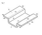
- FIG. 7 shows a perspective view of the shunt resistor 8.
- the wiring substrate 10 is arranged in the current detection circuit 100.
- the wiring substrate 10 is mounted with the microcomputer 1, the motor drive circuit 2, the current detection circuit 7, the shunt circuit 8, and the wirings 9a, 9b of the current detection device 100 shown in FIG. 1 .
- a plurality of lands 11 to 14 and wiring patterns 21 to 26 shown in FIGS. 2 and 3 are disposed on the surface of the wiring substrate 10.
- the lands 11 to 14 and the wiring patterns 21 to 26 are respectively formed by a conductor.
- the first land 11 and the second land 12 each has a rectangular portion, and is arranged at a predetermined interval with a virtual central line CL as the center.
- the areas of the first land 11 and the second land 12 are the same.
- the area of the third land 13 is smaller than that of the first land 11, and is arranged at one end (lower side in FIG. 2 ) in a direction parallel to the central line CL of the first land 11 and connected to the first land 11.
- the area of the fourth land 14 is smaller than that of the second land 12, and is arranged at one end (lower side in FIG. 2 ) in a direction parallel to the central line CL of the second land 12 and connected to the second land 12.
- the areas of the third land 13 and the fourth land 14 are the same.
- a concave part 15 formed by an insulator is arranged at the ends (lower side in FIG. 2 ) in a direction parallel to the central line CL of the third land 13 and the fourth land 14, and at the ends (upper side in FIG. 2 ) in a direction parallel to the central line CL of the first land 11 and the second land 12.
- the interval between the third land 13 and the fourth land 14 is greater than the interval between the first land 11 and the second land 12.
- the lands 11 to 14 form a land for mounting the shunt resistor 8.
- the first land 11 and the third land 13 are arranged at one end of the fifth wiring pattern 25.
- the second land 12 and the fourth land 14 are arranged at one end of the sixth wiring pattern 26.
- the other ends (not shown) of the fifth wiring pattern 25 and the sixth wiring pattern 26 are respectively connected to the motor drive circuit 2 and the motor 6 shown in FIG. 1 by way of another wiring pattern (not shown), the connector C, or the like.
- the fifth wiring pattern 25 and the sixth wiring pattern 26 configure one part of one wiring 9b for flowing the current from the motor drive circuit 2 to the motor 6.
- the first wiring pattern 21 is connected to an edge 13b on the central line CL side of the third land 13, and is pulled out from the third land 13 towards the fourth land 14.
- the second wiring pattern 22 is connected to an edge 14b on the central line CL side of the fourth land 13, and is pulled out from the fourth land 14 towards the third land 13.
- the third wiring pattern 23 is connected to the first wiring pattern 21, and is pulled in one direction (lower side in FIG. 2 ) parallel to the central line CL.
- the fourth wiring pattern 24 is connected to the second wiring pattern 22, and is pulled in one direction (lower side in FIG. 2 ) parallel to the central line CL.
- the ends (not shown) of the third wiring pattern 23 and the fourth wiring pattern 24 are respectively connected to the current detection circuit 7 (shown in FIG. 1 ) by way of other wiring patterns etc. (not shown).
- the wiring patterns 21 to 24 form a wiring pattern for detecting the potential different of both ends of the shunt resistor 8.
- a depression 27 is formed on the inner angle side of a connection part between the first wiring pattern 21 and the third wiring pattern 23.
- a depression 28 is formed on the inner angle side of a connection part between the second wiring pattern 22 and the fourth wiring pattern 24.
- the widths of the first wiring pattern 21 and the second wiring pattern 22 are made the same as the widths of the third wiring pattern 23 and the fourth wiring pattern 24 by forming the depressions 27, 28.
- the interval between the first land 11 and the first wiring pattern 21 and the interval between the second land 12 and the second wiring pattern 22 are smaller than the interval between the first land 11 and the second land 12.
- the lands 11 to 14 and the wiring patterns 21 to 26 are plane symmetric with respect to the central line CL.
- Portions other than the lands 11 to 14, that is, the periphery of the lands 11 to 14, the space between the lands 11 to 14, and the surface of each of the wiring patterns 21 to 26 are covered by a resist film 40 (shown in FIG. 5 and FIG. 6 ) so as to be insulated.
- the shunt resistor 8 has rectangular surfaces 81, 82 formed at both ends and a central part floating with respect to the rectangular surfaces 81, 82.
- one rectangular surface 81 of the shunt resistor 8 is mounted on the first land 11 and the third land 13, and the other rectangular surface 82 is mounted on the second land 12 and the fourth land 14.
- each of the rectangular surfaces 81, 82 of the shunt resistor 8 is mounted on each land 11 to 14 so that the edges 81 b, 82b (shown in FIG. 7 ) on the central part side of each of the rectangular surfaces 81, 82 of the shunt resistor 8 contact the edges 13b, 14b (shown in FIG.
- the hatching portion of rectangular shape surrounded by a chain double-dashed line on the lands 11 to 14 of FIG. 2 is the contacting portion of the rectangular surfaces 81, 82 of the shunt resistor 8 with respect to the lands 11 to 14.
- the edges other than the edges 81 b, 82b of each of the rectangular surfaces 81, 82 of the shunt resistor 8 are spaced apart from the edge of the opposing land 11 to 14 by a predetermined interval.
- the concave part 15 is used for positioning when mounting the shunt resistor 8 on the lands 11 to 14 as described above. Specifically, the concave part 15 is detected through image recognition, the cream solder is applied to an appropriate position on the lands 11 to 14 with the concave part 15 as a marker, and thereafter, the shunt resistor 8 is mounted to an appropriate position on the lands 11 to 14. Subsequently, when the solder melted through heat is cooled, the solder does not wet spread on the lands 11 to 14 and flow into the concave part 15, and shift of the shunt resistor 8 from the appropriate position is inhibited by the concave part 15.
- each of the rectangular surfaces 81, 82 of the shunt resistor 8 is mounted on the lands 11 to 14 as shown in FIG. 4 etc., and thereafter, the wiring substrate 10 and the shunt resistor 8 are once heated with a reflow bath etc. and cooled, so that the shunt resistor 8 is soldered to the lands 11 to 14 as shown in FIG. 5 and FIG. 6 .
- FIG. 5 shows that the shunt resistor 8 is soldered to the lands 11 to 14 as shown in FIG. 5 and FIG. 6 .
- a large solder fillet 30 forms from portions 83, 84 of the shunt resistor 8 floating from the first land 11 and the second land 12 to portions 11c, 12c on the central line CL side of the first land 11 and the second land 12 that are not contacting the rectangular surfaces 81, 82.
- the solder fillet 30 also forms from end faces 85a to 85c, 86a to 86c (shown in FIG. 4 to FIG.
- the wiring 9b shown in FIG. 1 becomes to allow a current to flow therethrough, whereby the drive current of the motor 6 flows through the wiring patterns 25, 26 and the shunt resistor 8.
- the potential difference between the both ends of the shunt resistor 8 is then detected through the wiring patterns 21 to 24 by the current detection circuit 7, and the current value flowing to the motor 6 is detected based on the potential difference and the current conversion data stored in advance.
- the soldering strength can be increased by mounting and soldering large part of each of the rectangular surfaces 81, 82 of the shunt resistor 8 to the first land 11 and the second land 12 having a large area, and enlarging the solder fillet 30 formed from the shunt resistor 8 to the first land 11 and the second land 12.
- cracks are less likely to form in the solder between the shunt resistor 8 and the wiring patterns 21, 22, and the potential difference between the both ends of the shunt resistor 8 and the current to be detected can be accurately detected without changing the wiring path for detecting the current to be detected (drive current of the motor 6) and the resistance value of the wiring path, and without being influenced by soldering.
- the resist film 40 exists between the portions 83, 84 of the shunt resistor 8 and the wiring patterns 21, 22.
- the fillet does not form between the portions 83, 84 of the shunt resistor 8 and the wiring patterns 21, 22. Since the fillet does not exist, cracks do not form near the portions 83, 84 of the shunt resistor 8. That is, the fillet does not influence current detection near the portions 83, 84 of the shunt resistor 8 and the wiring patterns 21, 22, and current can be accurately detected.
- the wiring path for detecting the current to be detected that is, the wiring patterns 21 to 24 can be separated from the wiring path through which the current to be detected flows, that is, the path from the land on one side of the central line CL (first land 11 and third land 13 or second land 12 and fourth land 14) to the land on the other side (second land 12 and fourth land 14 or first land 11 and third land 13) through the shunt resistor 8.
- the current to be detected does not flow into the wiring patterns 21 to 24, and the current to be detected can be accurately detected based on the potential difference between the both ends of the shunt resistor 8.
- the shunt resistor 8 is mounted on the lands 11 to 14 so that each of the rectangular surfaces 81, 82 of the shunt resistor 8 contacts the hatching portion in FIG. 2 , whereby the first land 11 and the second land 12 are widened towards the central line CL side from the edges 13b, 14b on the central line CL side of the third land 13 and the fourth land 14, and the areas of the first land 11 and the second land 12 are made larger than the areas of the rectangular surfaces 81, 82.
- the solder fillet 30 formed from the shunt resistor 8 towards the central line CL side of the first land 11 and the second land 12 can be enlarged to further increase the soldering strength, whereby generation of solder cracks is further prevented.
- the generated heat of the shunt resistor 8 that is generated when the current to be detected flows is radiated by the first land 11 and the second land 12, whereby the resistance value of the shunt resistor 8 is prevented from changing. Therefore, the potential difference between the both ends of the shunt resistor 8 and the current to be detected can be accurately detected continuously.
- the wiring patterns 21 to 24 can be easily pulled out from the third land 13 and the fourth land 14, and the degree of freedom of circuit design in the wiring substrate 10 can be enhanced.
- the lands 11 to 14 and the wiring patterns 21 to 26 are plane symmetric with the central line CL as the center, the wiring path for detecting the current to be detected and the resistance value of the wiring path become the same on both sides of the central line CL.
- the current to be detected can be easily and accurately detected based on the potential difference between the both ends of the shunt resistor 8 detected through the wiring patterns 21 to 24 without performing a complex correction or the like that takes variation in the lands 11 to 14 and the wiring patterns 21 to 26 into consideration.
- the current to be detected can be easily and accurately detected even if the current to be detected is flowed from either side (wiring pattern 25 side or wiring pattern 26 side) of the central line CL, whereby degree of freedom of arrangement and design of the lands 11 to 14, the wiring patterns 21 to 26, the electronic circuit, or the like in the wiring substrate 10 can be enhanced.
- the first land 11 and the second land 12 can be extended in the direction of the first wiring pattern 21 and the second wiring pattern 22 thereby increasing the area of the first land 11 and the second land 12.
- the solder fillet 30 formed from the shunt resistor 8 to the first land 11 and the second land 12 can be enlarged.
- the solder is disposed on the wiring patterns 21 to 24 and the shunt resistor 8 and the wiring patterns 21 to 24 tend to be joined by the solder when the mounting position of the shunt resistor 8 with respect to the lands 11 to 14 is shifted towards the central line CL side or the solder amount for joining the shunt resistor 8 and the lands 11 to 14 is large. Furthermore, since the width of the wiring patterns 21 to 24 is small, cracks easily form in the solder thereby changing the wiring path for detecting the current to be detected and the resistance value of the wiring path, whereby the potential difference in the shunt resistor 8 and the current to be detected may not be accurately detected.
- the shunt resistor 8 and the wiring patterns 21 to 24 are reliably prevented from being joined by the solder even if the mounting position of the shunt resistor 8 with respect to the lands 11 to 14 is shifted towards the central line side or the solder amount for joining the shunt resistor 8 and the lands 11 to 14 is large.
- the wiring path for detecting the current to be detected and the resistance value of the wiring path do not change, and the potential difference between the both ends of the shunt resistor 8 and the current to be detected can be accurately detected without being influenced by soldering.
- the wiring patterns 21, 22 can be pulled out from the location of the third land 13 and the fourth land 14 contacting the edges 81 b, 82b on the central part side of the rectangular surfaces 81, 82 of the shunt resistor 8 to have the width of each of the wiring patterns 21 to 24 constant.
- the variation in the resistance value of the first wiring pattern 21 and the third wiring pattern 23, and the resistance value of the second wiring pattern 22 and the fourth wiring pattern 24 is eliminated, and the current to be detected can be easily and accurately detected without performing a complex correction etc. that takes such a variation into consideration.
- the present invention is also applicable to a current detection device and a wiring substrate for detecting current flowing to other electronic circuits.
Landscapes
- Engineering & Computer Science (AREA)
- Microelectronics & Electronic Packaging (AREA)
- Manufacturing & Machinery (AREA)
- Physics & Mathematics (AREA)
- General Physics & Mathematics (AREA)
- Electric Connection Of Electric Components To Printed Circuits (AREA)
- Measuring Instrument Details And Bridges, And Automatic Balancing Devices (AREA)
- Measurement Of Current Or Voltage (AREA)
- Structures For Mounting Electric Components On Printed Circuit Boards (AREA)
- Structure Of Printed Boards (AREA)
Abstract
Description
- The present invention relates to a wiring substrate mounted with a shunt resistor for current detection of an electronic circuit, and a current detection device equipped with the wiring substrate.
- Conventionally, a shunt resistor is incorporated in the middle of a line through which the current of the electronic circuit flows, and the current is detected based on the voltage drop by the shunt resistor. In Japanese Patent Application Laid-Open No.
2002-5968 2003-121477 2003-121478 2003-121481 2003-121478 2003-121481 - In Japanese Patent Application Laid-Open No.
2003-232814 2002-372551 2002-372550 2003-121477 2003-121478 2003-121481 - Generally, both ends of the shunt resistor are soldered to the land of the substrate, but if cracks form in the solder between the shunt resistor and the wiring pattern, the wiring path for detecting the current to be detected changes and the resistance value of the wiring path changes, whereby the potential difference in the shunt resistor and the current to be detected cannot be accurately detected. In particular, if the area of the land is only slightly larger than the area of the surface of the shunt resistor contacting the land as in Japanese Patent Application Laid-Open No.
2002-5968 2002-372551 2002-372550 - In view of solving the above problems, it is an object of the present invention to provide a wiring substrate enabling accurately detection of the potential difference in the shunt resistor and the current to be detected without being influenced by soldering, and a current detection device.
- The present invention relates to a wiring substrate including a land mounted with each rectangular surface of a shunt resistor, which has the rectangular surface at each of both ends thereof and has a central part floating with respect to the rectangular surfaces, and a wiring pattern for detecting a potential difference between the both ends of the shunt resistor pulled out from the land; and a current connection device including the shunt resistor, the wiring substrate, and a current detection circuit for detecting the potential difference between the both ends of the shunt resistor through the wiring pattern and detecting a current flowing to an electronic circuit formed on the wiring substrate based on the potential difference, respectively having the following configuration.
The land is configured by a first land and a second land each having a rectangular portion and being arranged at a predetermined interval with a virtual central line as a center, a third land having an area smaller than that of the first land and being arranged at one end of a direction parallel to the central line of the first land to be connected to the first land, and a fourth land having an area smaller than that of the second land and being arranged at one end of a direction parallel to the central line of the second land to be connected to the second land.
The wiring pattern is configured by a first wiring pattern connected to the third land and pulled out from the third land towards the fourth land, a second wiring pattern connected to the fourth land and pulled out from the fourth land towards the third land, a third wiring pattern connected to the first wiring pattern and pulled out in one direction parallel to the central line, and a fourth wiring connected to the second wiring pattern and pulled out in one direction parallel to the central line. - Accordingly, large part of each of the rectangular surfaces of the shunt resistor is mounted on and soldered to the first land and the second land each having a large area, and the solder fillet formed from the shunt resistor to the first land and the second land is enlarged, thereby increasing the solder strength. Thus cracks are less likely to be formed in the solder between the shunt resistor and the wiring pattern, the wiring path for detecting the current to be detected and the resistance value of the wiring path do not change, and the potential difference between the both ends of the shunt resistor and the current to be detected flowing through the electronic circuit can be accurately detected. Since the wiring pattern for detecting potential difference in the shunt resistor is pulled out from the third land and the fourth land towards the fourth land and the third land, and then pulled out in one direction away from the third land and the fourth land, the wiring path for detecting the current to be detected, that is, the wiring patterns can be separated from the wiring path through which the current to be detected flows, that is, the path from the land on one side of the central line to the land on the other side through the shunt resistor. Thus, the current to be detected does not flow into the wiring patterns, and the current to be detected can be accurately detected based on the potential difference between the both ends of the shunt resistor.
- Further, in the wiring substrate of the present invention, the shunt resistor is soldered to the respective lands with one of the rectangular surfaces of the shunt resistor mounted on the first land and the third land, and the other rectangular surface mounted on the second land and the fourth land.
- Therefore, the current to be detected flows from the first land and the third land or the second land and the fourth to the second land and the fourth land or the first land and the third land through the shunt resistor, and does not flow into the wiring pattern, whereby the current to be detected can be accurately detected based on the potential difference between the both ends of the shunt resistor.
- Further, in the wiring substrate of the present invention, each of the rectangular surfaces of the shunt resistor is mounted on the respective lands so that an edge on a central part side of each of the rectangular surfaces of the shunt resistor contacts an edge on the central line side of the third land and the fourth land and a virtually extended line extending from the edge towards the first land and the second land.
- Therefore, the first land and the second land are widened towards the central line side from the edges on the central line side of the third land and the fourth land, and the areas of the first land and the second land are made larger than the areas of the rectangular surfaces of the shunt resistor. Thus, the solder fillet formed from the shunt resistor to the first land and the second land can be enlarged to further increase the soldering strength, whereby generation of solder cracks is prevented. The generated heat of the shunt resistor that is generated when the current to be detected flows is radiated by the first land and the second land, whereby the resistance value of the shunt resistor is prevented from changing. Therefore, the potential difference between the both ends of the shunt resistor and the current to be detected flowing through the electronic circuit can be accurately detected continuously.
- Further, in the wiring substrate of the present invention, a solder fillet is formed from a portion of the shunt resistor floating from the first land and the second land to a portion on the central line side of the first land and the second land.
- Therefore, since the solder fillet is large, the solder strength between the shunt resistor and each land becomes higher, and generation of solder cracks is more reliably prevented.
- Moreover, in the wiring substrate of the present invention, an interval between the third land and the fourth land is larger than the interval between the first land and the second land.
- Thus, the wiring patterns can be easily pulled out from the third land and the fourth land, and the degree of freedom of circuit design in the wiring substrate can be enhanced.
- Further, in the wiring substrate of the present invention, the land and the wiring pattern are plane symmetric with the central line as the center.
- The wiring path for detecting the current to be detected and the resistance value of the wiring path thus become the same on both sides of the central line, whereby the current to be detected can be easily and accurately detected based on the potential difference between the both ends of the shunt resistor detected through the wiring patterns without performing a complex correction or the like that takes variation in the lands and the wiring patterns into consideration. Moreover, the current to be detected can be easily and accurately detected even if the current to be detected is flowed from either side of the central line, whereby degree of freedom of arrangement and design of the lands, the wiring patterns, the electronic circuit, or the like in the wiring substrate can be enhanced.
- Further, in the wiring substrate of the present invention, an interval between the first land and the first wiring pattern and an interval between the second land and the second wiring pattern are smaller than the interval between the first land and the second land.
- Therefore, the first land and the second land are widened towards the first wiring pattern and the second wiring pattern, the areas of the first land and the second land are large, and the solder fillet formed from the shunt resistor to the first land and the second land is enlarged.
- Moreover, in the wiring substrate of the present invention, a surface of each of the wiring patterns is insulated.
- If the surface of each of the wiring patterns is not insulated, the solder is disposed on the wiring pattern and the shunt resistor and the wiring pattern tend to be joined by the solder when the mounting position of the shunt resistor with respect to the land is shifted towards the central line side or the solder amount for joining the shunt resistor and the land is large. Furthermore, since the width of the wiring pattern is small, cracks easily form in the solder thereby changing the wiring path for detecting the current to be detected and the resistance value of the wiring path, whereby the potential difference in the shunt resistor and the current to be detected may not be accurately detected. If the surface of each of the wiring patterns is insulated, the shunt resistor and the wiring pattern are reliably prevented from being joined by the solder even if the mounting position of the shunt resistor with respect to the land is shifted towards the central line side or the solder amount for joining the shunt resistor and the land is large. Thus, the wiring path for detecting the current to be detected and the resistance value of the wiring path do not change, and the potential difference between the both ends of the shunt resistor and the current to be detected flowing through the electronic circuit can be accurately detected without being influenced by soldering.
- In the wiring substrate of the present invention, a depression is formed on an inner angle side of a connection part between the first wiring pattern and the third wiring pattern, and a depression is formed on an inner angle side of a connection part between the second wiring pattern and the fourth wiring pattern.
- Therefore, of the wiring patterns can be pulled out from the location of the third land and the fourth land contacting the edges on the central part side of the rectangular surfaces of the shunt resistor to have the width of each of the wiring patterns constant, whereby the variation in the resistance value of the first wiring pattern and the third wiring pattern and the resistance value of the second wiring pattern and the fourth wiring pattern is eliminated, and the current to be detected can be easily and accurately detected without performing a complex correction etc. that takes such a variation into consideration.
- According to the present invention, the solder fillet formed from the shunt resistor to the first land and the second land is enlarged to increase the solder strength, cracks do not form in the solder between the shunt resistor and the wiring pattern, and the wiring path for detecting the current to be detected and the resistance value of the wiring path do not change, whereby the potential difference between the both ends of the shunt resistor and the current to be detected flowing through the electronic circuit can be accurately detected without being influenced by the solder.
-
FIG. 1 shows a view of a current detection device; -
FIG. 2 shows a plan view of main parts of a wiring substrate; -
FIG. 3 shows a perspective view of the main parts of the wiring substrate; -
FIG. 4 shows a perspective view of a state of a shunt resistor mounted on the wiring substrate; -
FIG. 5 shows a cross sectional view of a state of the shunt resistor soldered to the wiring substrate; -
FIG. 6 shows a cross sectional view of another state of the shunt resistor soldered to the wiring substrate; and -
Fig. 7 shows a perspective view of the shunt resistor. -
FIG. 1 shows a view of acurrent detection device 100 according to the present embodiment. Thecurrent detection device 100 is configured by an ECU (Electronic Control Unit) used in an electrically operated power steering system of an automobile, and the like. Thecurrent detection device 100 includes a microcomputer 1, amotor drive circuit 2, acurrent detection circuit 7, and ashunt resistor 8. A steering torque of a steering wheel detected by a torque sensor 4 and a vehicle speed (traveling speed) of the automobile detected by a vehicle speed sensor 5 are input to the microcomputer 1 via a connector C and a wiring. Power is supplied to the microcomputer 1 and themotor drive circuit 2 from a battery 3 via the connector C and the wiring. - The
motor drive circuit 2 is configured by an H bridge circuit including four FETS, an FET gate drive circuit, and a step-up power supply. Themotor 6 is configured by an electric motor. Themotor 6 is rotation driven to supply assistance force to the steering of the steering wheel. The microcomputer 1 determines a current command value for driving themotor 6 based on the steering torque, the vehicle speed, and the like, and outputs the current command value to themotor drive circuit 2. Themotor drive circuit 2 flows, in the forward direction or opposite direction, current of the level corresponding to the current command value to themotor 6 via thewiring 9a, 9b, the connector C and the like based on the current command value input from the microcomputer 1, and drives themotor 6 in PWM (Pulse Width Modulation) control. Theshunt resistor 8 is arranged in the middle of onewiring 9b for flowing current from themotor drive circuit 2 to themotor 6. Thecurrent detection circuit 7 detects the potential difference between the both ends of theshunt resistor 8, detects the current value flowing to themotor 6 based on the potential difference and current conversion data (graph or function) stored in advance, and outputs the same to the microcomputer 1. The microcomputer 1 feedback controls the current flowing to themotor 6. -
FIG. 2 shows a plan view of the main parts of awiring substrate 10 according to the present embodiment.FIG. 3 shows a perspective view of the main parts of thewiring substrate 10.FIG. 4 shows a perspective view showing a state of theshunt resistor 8 mounted on thewiring substrate 10.FIGS. 5 and 6 show cross sectional views showing a state of theshunt resistor 8 soldered to thewiring substrate 10. Specifically,FIG. 5 shows a cross sectional view taken along line A-A ofFIG. 4 , andFIG. 6 shows a cross sectional view taken along line B-B ofFIG. 4 .FIG. 7 shows a perspective view of theshunt resistor 8. - The
wiring substrate 10 is arranged in thecurrent detection circuit 100. Thewiring substrate 10 is mounted with the microcomputer 1, themotor drive circuit 2, thecurrent detection circuit 7, theshunt circuit 8, and thewirings 9a, 9b of thecurrent detection device 100 shown inFIG. 1 . A plurality oflands 11 to 14 andwiring patterns 21 to 26 shown inFIGS. 2 and3 are disposed on the surface of thewiring substrate 10. Thelands 11 to 14 and thewiring patterns 21 to 26 are respectively formed by a conductor. - As shown in
FIG. 2 , thefirst land 11 and thesecond land 12 each has a rectangular portion, and is arranged at a predetermined interval with a virtual central line CL as the center. The areas of thefirst land 11 and thesecond land 12 are the same. The area of thethird land 13 is smaller than that of thefirst land 11, and is arranged at one end (lower side inFIG. 2 ) in a direction parallel to the central line CL of thefirst land 11 and connected to thefirst land 11. The area of thefourth land 14 is smaller than that of thesecond land 12, and is arranged at one end (lower side inFIG. 2 ) in a direction parallel to the central line CL of thesecond land 12 and connected to thesecond land 12. The areas of thethird land 13 and thefourth land 14 are the same. Anedge 11a on the side opposite to the central line CL of thefirst land 11, and anedge 13a on the side opposite to the central line CL of thethird land 13 coincide. Anedge 12a on the side opposite to the central line CL of thesecond land 12 and anedge 14a on the side opposite to the central line CL of thefourth land 14 coincide. Aconcave part 15 formed by an insulator is arranged at the ends (lower side inFIG. 2 ) in a direction parallel to the central line CL of thethird land 13 and thefourth land 14, and at the ends (upper side inFIG. 2 ) in a direction parallel to the central line CL of thefirst land 11 and thesecond land 12. The interval between thethird land 13 and thefourth land 14 is greater than the interval between thefirst land 11 and thesecond land 12. Thelands 11 to 14 form a land for mounting theshunt resistor 8. - The
first land 11 and thethird land 13 are arranged at one end of thefifth wiring pattern 25. Thesecond land 12 and thefourth land 14 are arranged at one end of thesixth wiring pattern 26. The other ends (not shown) of thefifth wiring pattern 25 and thesixth wiring pattern 26 are respectively connected to themotor drive circuit 2 and themotor 6 shown inFIG. 1 by way of another wiring pattern (not shown), the connector C, or the like. Thefifth wiring pattern 25 and thesixth wiring pattern 26 configure one part of onewiring 9b for flowing the current from themotor drive circuit 2 to themotor 6. - As shown in
FIG. 2 , thefirst wiring pattern 21 is connected to anedge 13b on the central line CL side of thethird land 13, and is pulled out from thethird land 13 towards thefourth land 14. Thesecond wiring pattern 22 is connected to anedge 14b on the central line CL side of thefourth land 13, and is pulled out from thefourth land 14 towards thethird land 13. Thethird wiring pattern 23 is connected to thefirst wiring pattern 21, and is pulled in one direction (lower side inFIG. 2 ) parallel to the central line CL. Thefourth wiring pattern 24 is connected to thesecond wiring pattern 22, and is pulled in one direction (lower side inFIG. 2 ) parallel to the central line CL. The ends (not shown) of thethird wiring pattern 23 and thefourth wiring pattern 24 are respectively connected to the current detection circuit 7 (shown inFIG. 1 ) by way of other wiring patterns etc. (not shown). Thewiring patterns 21 to 24 form a wiring pattern for detecting the potential different of both ends of theshunt resistor 8. - As shown in
FIG. 2 andFIG. 3 , adepression 27 is formed on the inner angle side of a connection part between thefirst wiring pattern 21 and thethird wiring pattern 23. Adepression 28 is formed on the inner angle side of a connection part between thesecond wiring pattern 22 and thefourth wiring pattern 24. The widths of thefirst wiring pattern 21 and thesecond wiring pattern 22 are made the same as the widths of thethird wiring pattern 23 and thefourth wiring pattern 24 by forming thedepressions first land 11 and thefirst wiring pattern 21 and the interval between thesecond land 12 and thesecond wiring pattern 22 are smaller than the interval between thefirst land 11 and thesecond land 12. Thelands 11 to 14 and thewiring patterns 21 to 26 are plane symmetric with respect to the central line CL. Portions other than thelands 11 to 14, that is, the periphery of thelands 11 to 14, the space between thelands 11 to 14, and the surface of each of thewiring patterns 21 to 26 are covered by a resist film 40 (shown inFIG. 5 and FIG. 6 ) so as to be insulated. - As shown in
FIG. 7 , theshunt resistor 8 hasrectangular surfaces rectangular surfaces FIG. 4 to FIG. 6 , onerectangular surface 81 of theshunt resistor 8 is mounted on thefirst land 11 and thethird land 13, and the otherrectangular surface 82 is mounted on thesecond land 12 and thefourth land 14. Specifically, each of therectangular surfaces shunt resistor 8 is mounted on eachland 11 to 14 so that theedges FIG. 7 ) on the central part side of each of therectangular surfaces shunt resistor 8 contact theedges FIG. 2 ) on the central line CL side of thethird land 13 and thefourth land 14, and the virtually extended line EL (shown inFIG. 2 ) extending from theedges first land 11 and thesecond land 12. The hatching portion of rectangular shape surrounded by a chain double-dashed line on thelands 11 to 14 ofFIG. 2 is the contacting portion of therectangular surfaces shunt resistor 8 with respect to thelands 11 to 14. The edges other than theedges rectangular surfaces shunt resistor 8 are spaced apart from the edge of the opposingland 11 to 14 by a predetermined interval. Theconcave part 15 is used for positioning when mounting theshunt resistor 8 on thelands 11 to 14 as described above. Specifically, theconcave part 15 is detected through image recognition, the cream solder is applied to an appropriate position on thelands 11 to 14 with theconcave part 15 as a marker, and thereafter, theshunt resistor 8 is mounted to an appropriate position on thelands 11 to 14. Subsequently, when the solder melted through heat is cooled, the solder does not wet spread on thelands 11 to 14 and flow into theconcave part 15, and shift of theshunt resistor 8 from the appropriate position is inhibited by theconcave part 15. - After applying the cream solder on each
land 11 to 14 of thewiring substrate 10, each of therectangular surfaces shunt resistor 8 is mounted on thelands 11 to 14 as shown inFIG. 4 etc., and thereafter, thewiring substrate 10 and theshunt resistor 8 are once heated with a reflow bath etc. and cooled, so that theshunt resistor 8 is soldered to thelands 11 to 14 as shown inFIG. 5 and FIG. 6 . At this point, as shown inFIG. 5 , alarge solder fillet 30 forms fromportions shunt resistor 8 floating from thefirst land 11 and thesecond land 12 toportions first land 11 and thesecond land 12 that are not contacting therectangular surfaces FIG. 5 and FIG. 6 , thesolder fillet 30 also forms from end faces 85a to 85c, 86a to 86c (shown inFIG. 4 to FIG. 7 ) orthogonal to each of therectangular surfaces shunt resistor 8 to the portion of thelands 11 to 14 proximate to the end faces 85a to 85c, 86a to 86c that are not contacting therectangular surfaces shunt resistor 8 and thewiring patterns 21 to 26 will not be soldered since the periphery of thelands 11 to 14, the space between thelands 11 to 14, and the surface of each of thewiring patterns 21 to 26 are insulated. - When the
shunt resistor 8 is soldered to thelands 11 to 14 as described above, thewiring 9b shown inFIG. 1 becomes to allow a current to flow therethrough, whereby the drive current of themotor 6 flows through thewiring patterns shunt resistor 8. The potential difference between the both ends of theshunt resistor 8 is then detected through thewiring patterns 21 to 24 by thecurrent detection circuit 7, and the current value flowing to themotor 6 is detected based on the potential difference and the current conversion data stored in advance. - Therefore, the soldering strength can be increased by mounting and soldering large part of each of the
rectangular surfaces shunt resistor 8 to thefirst land 11 and thesecond land 12 having a large area, and enlarging thesolder fillet 30 formed from theshunt resistor 8 to thefirst land 11 and thesecond land 12. Thus, cracks are less likely to form in the solder between theshunt resistor 8 and thewiring patterns shunt resistor 8 and the current to be detected can be accurately detected without changing the wiring path for detecting the current to be detected (drive current of the motor 6) and the resistance value of the wiring path, and without being influenced by soldering. - As shown in the cross sectional view of
FIG. 6 , the resistfilm 40 exists between theportions shunt resistor 8 and thewiring patterns portions shunt resistor 8 and thewiring patterns portions shunt resistor 8. That is, the fillet does not influence current detection near theportions shunt resistor 8 and thewiring patterns - Since the
wiring patterns 21 to 24 for detecting potential difference in theshunt resistor 8 are pulled out from thethird land 13 and thefourth land 14 towards thefourth land 14 and thethird land 13, and then pulled out in one direction away from thethird land 13 and thefourth land 14, the wiring path for detecting the current to be detected, that is, thewiring patterns 21 to 24 can be separated from the wiring path through which the current to be detected flows, that is, the path from the land on one side of the central line CL (first land 11 andthird land 13 orsecond land 12 and fourth land 14) to the land on the other side (second land 12 andfourth land 14 orfirst land 11 and third land 13) through theshunt resistor 8. Thus, the current to be detected does not flow into thewiring patterns 21 to 24, and the current to be detected can be accurately detected based on the potential difference between the both ends of theshunt resistor 8. - The
shunt resistor 8 is mounted on thelands 11 to 14 so that each of therectangular surfaces shunt resistor 8 contacts the hatching portion inFIG. 2 , whereby thefirst land 11 and thesecond land 12 are widened towards the central line CL side from theedges third land 13 and thefourth land 14, and the areas of thefirst land 11 and thesecond land 12 are made larger than the areas of therectangular surfaces FIG. 5 , thesolder fillet 30 formed from theshunt resistor 8 towards the central line CL side of thefirst land 11 and thesecond land 12 can be enlarged to further increase the soldering strength, whereby generation of solder cracks is further prevented. The generated heat of theshunt resistor 8 that is generated when the current to be detected flows is radiated by thefirst land 11 and thesecond land 12, whereby the resistance value of theshunt resistor 8 is prevented from changing. Therefore, the potential difference between the both ends of theshunt resistor 8 and the current to be detected can be accurately detected continuously. - Since the interval between the
third land 13 and thefourth land 14 is larger than the interval between thefirst land 11 and thesecond land 12, thewiring patterns 21 to 24 can be easily pulled out from thethird land 13 and thefourth land 14, and the degree of freedom of circuit design in thewiring substrate 10 can be enhanced. - Furthermore, since the
lands 11 to 14 and thewiring patterns 21 to 26 are plane symmetric with the central line CL as the center, the wiring path for detecting the current to be detected and the resistance value of the wiring path become the same on both sides of the central line CL. Thus, the current to be detected can be easily and accurately detected based on the potential difference between the both ends of theshunt resistor 8 detected through thewiring patterns 21 to 24 without performing a complex correction or the like that takes variation in thelands 11 to 14 and thewiring patterns 21 to 26 into consideration. Moreover, the current to be detected can be easily and accurately detected even if the current to be detected is flowed from either side (wiring pattern 25 side orwiring pattern 26 side) of the central line CL, whereby degree of freedom of arrangement and design of thelands 11 to 14, thewiring patterns 21 to 26, the electronic circuit, or the like in thewiring substrate 10 can be enhanced. - Since the interval between the
first land 11 and thefirst wiring pattern 21 and the interval between thesecond land 12 and thesecond wiring pattern 22 are smaller than the interval between thefirst land 11 and thesecond land 12, thefirst land 11 and thesecond land 12 can be extended in the direction of thefirst wiring pattern 21 and thesecond wiring pattern 22 thereby increasing the area of thefirst land 11 and thesecond land 12. Thus, thesolder fillet 30 formed from theshunt resistor 8 to thefirst land 11 and thesecond land 12 can be enlarged. - If the surface of the
wiring patterns 21 to 24 is not insulated, the solder is disposed on thewiring patterns 21 to 24 and theshunt resistor 8 and thewiring patterns 21 to 24 tend to be joined by the solder when the mounting position of theshunt resistor 8 with respect to thelands 11 to 14 is shifted towards the central line CL side or the solder amount for joining theshunt resistor 8 and thelands 11 to 14 is large. Furthermore, since the width of thewiring patterns 21 to 24 is small, cracks easily form in the solder thereby changing the wiring path for detecting the current to be detected and the resistance value of the wiring path, whereby the potential difference in theshunt resistor 8 and the current to be detected may not be accurately detected. If the surface of thewiring patterns 21 to 24 is insulated, theshunt resistor 8 and thewiring patterns 21 to 24 are reliably prevented from being joined by the solder even if the mounting position of theshunt resistor 8 with respect to thelands 11 to 14 is shifted towards the central line side or the solder amount for joining theshunt resistor 8 and thelands 11 to 14 is large. Thus, the wiring path for detecting the current to be detected and the resistance value of the wiring path do not change, and the potential difference between the both ends of theshunt resistor 8 and the current to be detected can be accurately detected without being influenced by soldering. - Furthermore, since the
depressions wiring patterns 21 to 24, thewiring patterns third land 13 and thefourth land 14 contacting theedges rectangular surfaces shunt resistor 8 to have the width of each of thewiring patterns 21 to 24 constant. Thus, the variation in the resistance value of thefirst wiring pattern 21 and thethird wiring pattern 23, and the resistance value of thesecond wiring pattern 22 and thefourth wiring pattern 24 is eliminated, and the current to be detected can be easily and accurately detected without performing a complex correction etc. that takes such a variation into consideration. - In the embodiment described above, an example of applying the present invention to the
wiring substrate 10 and thecurrent detection device 100 for detecting the motor drive current in the electrically operated power steering system has been described, but the present invention is also applicable to a current detection device and a wiring substrate for detecting current flowing to other electronic circuits.
Claims (10)
- A wiring substrate comprising: a land mounted with each rectangular surface of a shunt resistor which has the rectangular surface at each of both ends thereof and has a central part floating with respect to the rectangular surfaces; and a wiring pattern for detecting a potential difference between the both ends of the shunt resistor pulled out from the land; wherein
the land is configured by:a first land and a second land each having a rectangular portion and being arranged at a predetermined interval with a virtual central line as a center;a third land having an area smaller than that of the first land and being arranged at one end of a direction parallel to the central line of the first land to be connected to the first land; anda fourth land having an area smaller than that of the second land and being arranged at one end of a direction parallel to the central line of the second land to be connected to the second land, andthe wiring pattern is configured by:a first wiring pattern connected to the third land and pulled out from the third land towards the fourth land;a second wiring pattern connected to the fourth land and pulled out from the fourth land towards the third land;a third wiring pattern connected to the first wiring pattern and pulled out in one direction parallel to the central line; anda fourth wiring connected to the second wiring pattern and pulled out in one direction parallel to the central line. - The wiring substrate according to claim 1, wherein the shunt resistor is soldered to the respective lands with one of the rectangular surfaces of the shunt resistor mounted on the first land and the third land, and the other rectangular surface mounted on the second land and the fourth land.
- The wiring substrate according to claim 2, wherein each of the rectangular surfaces of the shunt resistor is mounted on the respective lands so that an edge on a central part side of each of the rectangular surfaces of the shunt resistor contacts an edge on the central line side of the third land and the fourth land and a virtually extended line extending from the edge towards the first land and the second land.
- The wiring substrate according to claim 3, wherein a solder fillet is formed from a portion of the shunt resistor floating from the first land and the second land to a portion on the central line side of the first land and the second land.
- The wiring substrate according to claim 1, wherein an interval between the third land and the fourth land is larger than the interval between the first land and the second land.
- The wiring substrate according to claim 1, wherein the land and the wiring pattern are plane symmetric with the central line as the center.
- The wiring substrate according to claim 1, wherein an interval between the first land and the first wiring pattern and an interval between the second land and the second wiring pattern are smaller than the interval between the first land and the second land.
- The wiring substrate according to claim 1, wherein a surface of each of the wiring patterns is insulated.
- The wiring substrate according to claim 1, wherein a depression is formed on an inner angle side of a connection part between the first wiring pattern and the third wiring pattern, and a depression is formed on an inner angle side of a connection part between the second wiring pattern and the fourth wiring pattern.
- A current connection device comprising: a shunt resistor having a rectangular surface at each of both ends thereof and having a central part floating with respect to the rectangular surfaces; a wiring substrate arranged with a land mounted with each of the rectangular surfaces of the shunt resistor and a wiring pattern for detecting a potential difference between the both ends of the shunt resistor pulled out from the land; and a current detection circuit for detecting the potential difference between the both ends of the shunt resistor through the wiring pattern and detecting a current flowing to an electronic circuit formed on the wiring substrate based on the potential difference; wherein
the land of the wiring substrate is configured by:a first land and a second land each having a rectangular portion and being arranged at a predetermined interval with a virtual central line as a center;a third land having an area smaller than that of the first land and being arranged at one end of a direction parallel to the central line of the first land to be connected to the first land, anda fourth land having an area smaller than that of the second land and being arranged at one end of a direction parallel to the central line of the second land to be connected to the second land, andthe wiring pattern of the wiring substrate is configured by:a first wiring pattern connected to the third land and pulled out from the third land towards the fourth land;a second wiring pattern connected to the fourth land and pulled out from the fourth land towards the third land;a third wiring pattern connected to the first wiring pattern and pulled out in one direction parallel to the central line; anda fourth wiring connected to the second wiring pattern and pulled out in one direction parallel to the central line.
Applications Claiming Priority (1)
| Application Number | Priority Date | Filing Date | Title |
|---|---|---|---|
| JP2007118731A JP2008275418A (en) | 2007-04-27 | 2007-04-27 | Wiring board, current detection device |
Publications (3)
| Publication Number | Publication Date |
|---|---|
| EP1986479A2 true EP1986479A2 (en) | 2008-10-29 |
| EP1986479A3 EP1986479A3 (en) | 2009-08-05 |
| EP1986479B1 EP1986479B1 (en) | 2013-03-20 |
Family
ID=39672124
Family Applications (1)
| Application Number | Title | Priority Date | Filing Date |
|---|---|---|---|
| EP08153463A Not-in-force EP1986479B1 (en) | 2007-04-27 | 2008-03-27 | Wiring substrate and current detection device |
Country Status (5)
| Country | Link |
|---|---|
| US (1) | US20080265872A1 (en) |
| EP (1) | EP1986479B1 (en) |
| JP (1) | JP2008275418A (en) |
| CN (1) | CN101294987A (en) |
| RU (1) | RU2008116548A (en) |
Cited By (3)
| Publication number | Priority date | Publication date | Assignee | Title |
|---|---|---|---|---|
| EP3223307A4 (en) * | 2014-11-20 | 2018-08-29 | NSK Ltd. | Heat dissipation substrate for mounting electric component |
| EP3223308A4 (en) * | 2014-11-20 | 2018-08-29 | NSK Ltd. | Heat dissipation substrate for mounting electric component |
| CN117646200A (en) * | 2023-12-08 | 2024-03-05 | 江西景旺精密电路有限公司 | Method for improving potential difference nickel corrosion of deposited nickel-gold |
Families Citing this family (11)
| Publication number | Priority date | Publication date | Assignee | Title |
|---|---|---|---|---|
| JP2012175015A (en) * | 2011-02-24 | 2012-09-10 | Koa Corp | Resistor |
| JP6131018B2 (en) * | 2012-10-08 | 2017-05-17 | 株式会社デンソー | Shunt resistor and mounting method thereof |
| JP6364169B2 (en) * | 2013-10-23 | 2018-07-25 | Koa株式会社 | Shunt resistor and its resistance value measuring method |
| JP6344163B2 (en) * | 2014-09-03 | 2018-06-20 | 株式会社デンソー | Shunt resistor |
| JP6384211B2 (en) * | 2014-09-03 | 2018-09-05 | 株式会社デンソー | Shunt resistor |
| JP6413201B2 (en) * | 2015-10-02 | 2018-10-31 | 新電元工業株式会社 | Shunt resistor mounting structure and manufacturing method of shunt resistor mounting structure |
| JP6815772B2 (en) * | 2016-07-13 | 2021-01-20 | Koa株式会社 | Current measuring device |
| JP6989305B2 (en) * | 2017-06-30 | 2022-01-05 | 日本電産サンキョー株式会社 | Circuit board and motor controller |
| CN108020704B (en) * | 2017-11-27 | 2019-08-16 | 清华大学 | A Lightning Basal Current Inversion Method Based on Deconvolution |
| DE102019108541A1 (en) * | 2019-04-02 | 2020-10-08 | Eberspächer Controls Landau Gmbh & Co. Kg | Current measuring module |
| CN114664210B (en) * | 2022-03-29 | 2025-05-13 | 京东方科技集团股份有限公司 | Test substrate, test circuit, display panel and test assembly |
Citations (7)
| Publication number | Priority date | Publication date | Assignee | Title |
|---|---|---|---|---|
| JP2002005968A (en) | 2000-06-16 | 2002-01-09 | Unisia Jecs Corp | Current detector |
| JP2002372551A (en) | 2001-06-14 | 2002-12-26 | Koa Corp | Mounting structure of current detecting resistor |
| JP2002372550A (en) | 2001-06-14 | 2002-12-26 | Koa Corp | Current detecting resistor |
| JP2003121481A (en) | 2001-10-15 | 2003-04-23 | Koa Corp | Device and method for measuring inductance of current sensing low resistor |
| JP2003121478A (en) | 2001-10-15 | 2003-04-23 | Koa Corp | Voltage detection circuit for current detecting resistor |
| JP2003121477A (en) | 2001-10-15 | 2003-04-23 | Koa Corp | Structure and method for mounting current detecting resistor |
| JP2003232814A (en) | 2002-02-06 | 2003-08-22 | Toshiba Corp | Current detecting device and current detecting device for inverter |
Family Cites Families (8)
| Publication number | Priority date | Publication date | Assignee | Title |
|---|---|---|---|---|
| DE4339551C1 (en) * | 1993-11-19 | 1994-10-13 | Heusler Isabellenhuette | Resistor, constructed as a surface-mounted device, and method for its production, as well as a printed circuit board having such a resistor |
| JP3379240B2 (en) * | 1994-10-13 | 2003-02-24 | 富士電機株式会社 | Four-terminal shunt resistor |
| GB2361360B (en) * | 2000-04-13 | 2003-08-13 | Omega Res Ltd | Adaptors for electronic components |
| US6798189B2 (en) * | 2001-06-14 | 2004-09-28 | Koa Corporation | Current detection resistor, mounting structure thereof and method of measuring effective inductance |
| JP3826749B2 (en) * | 2001-08-22 | 2006-09-27 | 株式会社日立製作所 | Power converter with shunt resistor |
| DE20117650U1 (en) * | 2001-10-29 | 2003-03-13 | Isabellenhütte Heusler GmbH KG, 35683 Dillenburg | Surface mount electrical resistance |
| JP4452196B2 (en) * | 2004-05-20 | 2010-04-21 | コーア株式会社 | Metal plate resistor |
| US7190252B2 (en) * | 2005-02-25 | 2007-03-13 | Vishay Dale Electronics, Inc. | Surface mount electrical resistor with thermally conductive, electrically insulative filler and method for using same |
-
2007
- 2007-04-27 JP JP2007118731A patent/JP2008275418A/en not_active Withdrawn
-
2008
- 2008-03-27 EP EP08153463A patent/EP1986479B1/en not_active Not-in-force
- 2008-04-24 US US12/108,780 patent/US20080265872A1/en not_active Abandoned
- 2008-04-25 RU RU2008116548/28A patent/RU2008116548A/en not_active Application Discontinuation
- 2008-04-28 CN CNA2008100948206A patent/CN101294987A/en active Pending
Patent Citations (7)
| Publication number | Priority date | Publication date | Assignee | Title |
|---|---|---|---|---|
| JP2002005968A (en) | 2000-06-16 | 2002-01-09 | Unisia Jecs Corp | Current detector |
| JP2002372551A (en) | 2001-06-14 | 2002-12-26 | Koa Corp | Mounting structure of current detecting resistor |
| JP2002372550A (en) | 2001-06-14 | 2002-12-26 | Koa Corp | Current detecting resistor |
| JP2003121481A (en) | 2001-10-15 | 2003-04-23 | Koa Corp | Device and method for measuring inductance of current sensing low resistor |
| JP2003121478A (en) | 2001-10-15 | 2003-04-23 | Koa Corp | Voltage detection circuit for current detecting resistor |
| JP2003121477A (en) | 2001-10-15 | 2003-04-23 | Koa Corp | Structure and method for mounting current detecting resistor |
| JP2003232814A (en) | 2002-02-06 | 2003-08-22 | Toshiba Corp | Current detecting device and current detecting device for inverter |
Cited By (5)
| Publication number | Priority date | Publication date | Assignee | Title |
|---|---|---|---|---|
| EP3223307A4 (en) * | 2014-11-20 | 2018-08-29 | NSK Ltd. | Heat dissipation substrate for mounting electric component |
| EP3223308A4 (en) * | 2014-11-20 | 2018-08-29 | NSK Ltd. | Heat dissipation substrate for mounting electric component |
| US10249558B2 (en) | 2014-11-20 | 2019-04-02 | Nsk Ltd. | Electronic part mounting heat-dissipating substrate |
| US10388596B2 (en) | 2014-11-20 | 2019-08-20 | Nsk Ltd. | Electronic part mounting heat-dissipating substrate |
| CN117646200A (en) * | 2023-12-08 | 2024-03-05 | 江西景旺精密电路有限公司 | Method for improving potential difference nickel corrosion of deposited nickel-gold |
Also Published As
| Publication number | Publication date |
|---|---|
| EP1986479A3 (en) | 2009-08-05 |
| US20080265872A1 (en) | 2008-10-30 |
| CN101294987A (en) | 2008-10-29 |
| EP1986479B1 (en) | 2013-03-20 |
| RU2008116548A (en) | 2009-10-27 |
| JP2008275418A (en) | 2008-11-13 |
Similar Documents
| Publication | Publication Date | Title |
|---|---|---|
| EP1986479B1 (en) | Wiring substrate and current detection device | |
| JP5807721B2 (en) | Semiconductor module | |
| US10388596B2 (en) | Electronic part mounting heat-dissipating substrate | |
| KR20180120789A (en) | Electronic control device | |
| JP2013103535A (en) | Electronic control unit for electric power steering | |
| US20150274197A1 (en) | Electronic controller for electric power steering | |
| JP5741772B2 (en) | Semiconductor module | |
| JP6083461B2 (en) | Semiconductor module | |
| CN106716723B (en) | The attachment means of mulitpolar leads part and substrate | |
| WO2014122883A1 (en) | Multipole connector | |
| CN110654325B (en) | Circuit structure | |
| WO2015046050A1 (en) | Jumper element or current detection resistor element | |
| JP2013103534A (en) | Electronic control unit for electric power steering | |
| US10617018B2 (en) | Circuit board and control device | |
| KR102229077B1 (en) | Connection terminal assembly and circuit board using the connection terminal assembly | |
| JP2002134860A (en) | Flexible printed wiring board | |
| JP6445068B2 (en) | Electronic control unit | |
| WO2026013753A1 (en) | Electronic control device, drive device, and steering control device | |
| JP5184044B2 (en) | Printed wiring board unit | |
| JP2005216622A (en) | Welding structure for electric parts and method for welding electric parts | |
| JP2004296734A (en) | Electronic component mounting method | |
| JPH07147479A (en) | Conductive foil for printed wiring board | |
| JP2015069990A (en) | Semiconductor module | |
| JP2014204534A (en) | Power module | |
| JP2001313110A (en) | Connections structure of electric component |
Legal Events
| Date | Code | Title | Description |
|---|---|---|---|
| PUAI | Public reference made under article 153(3) epc to a published international application that has entered the european phase |
Free format text: ORIGINAL CODE: 0009012 |
|
| AK | Designated contracting states |
Kind code of ref document: A2 Designated state(s): AT BE BG CH CY CZ DE DK EE ES FI FR GB GR HR HU IE IS IT LI LT LU LV MC MT NL NO PL PT RO SE SI SK TR |
|
| AX | Request for extension of the european patent |
Extension state: AL BA MK RS |
|
| RIN1 | Information on inventor provided before grant (corrected) |
Inventor name: NAGASHIMA, ATSUSHIOMRON CORPORATION |
|
| RIN1 | Information on inventor provided before grant (corrected) |
Inventor name: NAGASHIMA, ATSUSHIC/O OMRON CORPORATION |
|
| RIN1 | Information on inventor provided before grant (corrected) |
Inventor name: NAGASHIMA, ATSUSHIC/O OMRON CORPORATION |
|
| PUAL | Search report despatched |
Free format text: ORIGINAL CODE: 0009013 |
|
| AK | Designated contracting states |
Kind code of ref document: A3 Designated state(s): AT BE BG CH CY CZ DE DK EE ES FI FR GB GR HR HU IE IS IT LI LT LU LV MC MT NL NO PL PT RO SE SI SK TR |
|
| AX | Request for extension of the european patent |
Extension state: AL BA MK RS |
|
| 17P | Request for examination filed |
Effective date: 20100204 |
|
| AKX | Designation fees paid |
Designated state(s): AT BE BG CH CY CZ DE DK EE ES FI FR GB GR HR HU IE IS IT LI LT LU LV MC MT NL NO PL PT RO SE SI SK TR |
|
| RAP1 | Party data changed (applicant data changed or rights of an application transferred) |
Owner name: OMRON AUTOMOTIVE ELECTRONICS CO., LTD. |
|
| 17Q | First examination report despatched |
Effective date: 20110307 |
|
| GRAP | Despatch of communication of intention to grant a patent |
Free format text: ORIGINAL CODE: EPIDOSNIGR1 |
|
| RIC1 | Information provided on ipc code assigned before grant |
Ipc: H05K 3/34 20060101AFI20120824BHEP Ipc: H05K 1/11 20060101ALI20120824BHEP Ipc: G01R 1/20 20060101ALI20120824BHEP Ipc: G01R 15/14 20060101ALI20120824BHEP |
|
| GRAS | Grant fee paid |
Free format text: ORIGINAL CODE: EPIDOSNIGR3 |
|
| GRAA | (expected) grant |
Free format text: ORIGINAL CODE: 0009210 |
|
| AK | Designated contracting states |
Kind code of ref document: B1 Designated state(s): AT BE BG CH CY CZ DE DK EE ES FI FR GB GR HR HU IE IS IT LI LT LU LV MC MT NL NO PL PT RO SE SI SK TR |
|
| REG | Reference to a national code |
Ref country code: GB Ref legal event code: FG4D |
|
| REG | Reference to a national code |
Ref country code: CH Ref legal event code: EP |
|
| REG | Reference to a national code |
Ref country code: IE Ref legal event code: FG4D |
|
| REG | Reference to a national code |
Ref country code: AT Ref legal event code: REF Ref document number: 602737 Country of ref document: AT Kind code of ref document: T Effective date: 20130415 |
|
| REG | Reference to a national code |
Ref country code: DE Ref legal event code: R096 Ref document number: 602008022983 Country of ref document: DE Effective date: 20130516 |
|
| PG25 | Lapsed in a contracting state [announced via postgrant information from national office to epo] |
Ref country code: LT Free format text: LAPSE BECAUSE OF FAILURE TO SUBMIT A TRANSLATION OF THE DESCRIPTION OR TO PAY THE FEE WITHIN THE PRESCRIBED TIME-LIMIT Effective date: 20130320 Ref country code: ES Free format text: LAPSE BECAUSE OF FAILURE TO SUBMIT A TRANSLATION OF THE DESCRIPTION OR TO PAY THE FEE WITHIN THE PRESCRIBED TIME-LIMIT Effective date: 20130701 Ref country code: SE Free format text: LAPSE BECAUSE OF FAILURE TO SUBMIT A TRANSLATION OF THE DESCRIPTION OR TO PAY THE FEE WITHIN THE PRESCRIBED TIME-LIMIT Effective date: 20130320 Ref country code: NO Free format text: LAPSE BECAUSE OF FAILURE TO SUBMIT A TRANSLATION OF THE DESCRIPTION OR TO PAY THE FEE WITHIN THE PRESCRIBED TIME-LIMIT Effective date: 20130620 Ref country code: BG Free format text: LAPSE BECAUSE OF FAILURE TO SUBMIT A TRANSLATION OF THE DESCRIPTION OR TO PAY THE FEE WITHIN THE PRESCRIBED TIME-LIMIT Effective date: 20130620 |
|
| REG | Reference to a national code |
Ref country code: AT Ref legal event code: MK05 Ref document number: 602737 Country of ref document: AT Kind code of ref document: T Effective date: 20130320 |
|
| REG | Reference to a national code |
Ref country code: LT Ref legal event code: MG4D |
|
| PG25 | Lapsed in a contracting state [announced via postgrant information from national office to epo] |
Ref country code: FI Free format text: LAPSE BECAUSE OF FAILURE TO SUBMIT A TRANSLATION OF THE DESCRIPTION OR TO PAY THE FEE WITHIN THE PRESCRIBED TIME-LIMIT Effective date: 20130320 Ref country code: LV Free format text: LAPSE BECAUSE OF FAILURE TO SUBMIT A TRANSLATION OF THE DESCRIPTION OR TO PAY THE FEE WITHIN THE PRESCRIBED TIME-LIMIT Effective date: 20130320 Ref country code: SI Free format text: LAPSE BECAUSE OF FAILURE TO SUBMIT A TRANSLATION OF THE DESCRIPTION OR TO PAY THE FEE WITHIN THE PRESCRIBED TIME-LIMIT Effective date: 20130320 Ref country code: GR Free format text: LAPSE BECAUSE OF FAILURE TO SUBMIT A TRANSLATION OF THE DESCRIPTION OR TO PAY THE FEE WITHIN THE PRESCRIBED TIME-LIMIT Effective date: 20130621 |
|
| REG | Reference to a national code |
Ref country code: NL Ref legal event code: VDEP Effective date: 20130320 |
|
| PG25 | Lapsed in a contracting state [announced via postgrant information from national office to epo] |
Ref country code: HR Free format text: LAPSE BECAUSE OF FAILURE TO SUBMIT A TRANSLATION OF THE DESCRIPTION OR TO PAY THE FEE WITHIN THE PRESCRIBED TIME-LIMIT Effective date: 20130320 Ref country code: BE Free format text: LAPSE BECAUSE OF FAILURE TO SUBMIT A TRANSLATION OF THE DESCRIPTION OR TO PAY THE FEE WITHIN THE PRESCRIBED TIME-LIMIT Effective date: 20130320 |
|
| PG25 | Lapsed in a contracting state [announced via postgrant information from national office to epo] |
Ref country code: RO Free format text: LAPSE BECAUSE OF FAILURE TO SUBMIT A TRANSLATION OF THE DESCRIPTION OR TO PAY THE FEE WITHIN THE PRESCRIBED TIME-LIMIT Effective date: 20130320 Ref country code: EE Free format text: LAPSE BECAUSE OF FAILURE TO SUBMIT A TRANSLATION OF THE DESCRIPTION OR TO PAY THE FEE WITHIN THE PRESCRIBED TIME-LIMIT Effective date: 20130320 Ref country code: CZ Free format text: LAPSE BECAUSE OF FAILURE TO SUBMIT A TRANSLATION OF THE DESCRIPTION OR TO PAY THE FEE WITHIN THE PRESCRIBED TIME-LIMIT Effective date: 20130320 Ref country code: SK Free format text: LAPSE BECAUSE OF FAILURE TO SUBMIT A TRANSLATION OF THE DESCRIPTION OR TO PAY THE FEE WITHIN THE PRESCRIBED TIME-LIMIT Effective date: 20130320 Ref country code: NL Free format text: LAPSE BECAUSE OF FAILURE TO SUBMIT A TRANSLATION OF THE DESCRIPTION OR TO PAY THE FEE WITHIN THE PRESCRIBED TIME-LIMIT Effective date: 20130320 Ref country code: PT Free format text: LAPSE BECAUSE OF FAILURE TO SUBMIT A TRANSLATION OF THE DESCRIPTION OR TO PAY THE FEE WITHIN THE PRESCRIBED TIME-LIMIT Effective date: 20130722 Ref country code: AT Free format text: LAPSE BECAUSE OF FAILURE TO SUBMIT A TRANSLATION OF THE DESCRIPTION OR TO PAY THE FEE WITHIN THE PRESCRIBED TIME-LIMIT Effective date: 20130320 Ref country code: IS Free format text: LAPSE BECAUSE OF FAILURE TO SUBMIT A TRANSLATION OF THE DESCRIPTION OR TO PAY THE FEE WITHIN THE PRESCRIBED TIME-LIMIT Effective date: 20130720 Ref country code: MC Free format text: LAPSE BECAUSE OF NON-PAYMENT OF DUE FEES Effective date: 20130331 |
|
| REG | Reference to a national code |
Ref country code: CH Ref legal event code: PL |
|
| PG25 | Lapsed in a contracting state [announced via postgrant information from national office to epo] |
Ref country code: CY Free format text: LAPSE BECAUSE OF FAILURE TO SUBMIT A TRANSLATION OF THE DESCRIPTION OR TO PAY THE FEE WITHIN THE PRESCRIBED TIME-LIMIT Effective date: 20130320 Ref country code: PL Free format text: LAPSE BECAUSE OF FAILURE TO SUBMIT A TRANSLATION OF THE DESCRIPTION OR TO PAY THE FEE WITHIN THE PRESCRIBED TIME-LIMIT Effective date: 20130320 |
|
| REG | Reference to a national code |
Ref country code: IE Ref legal event code: MM4A |
|
| PLBE | No opposition filed within time limit |
Free format text: ORIGINAL CODE: 0009261 |
|
| STAA | Information on the status of an ep patent application or granted ep patent |
Free format text: STATUS: NO OPPOSITION FILED WITHIN TIME LIMIT |
|
| PG25 | Lapsed in a contracting state [announced via postgrant information from national office to epo] |
Ref country code: LI Free format text: LAPSE BECAUSE OF NON-PAYMENT OF DUE FEES Effective date: 20130331 Ref country code: IE Free format text: LAPSE BECAUSE OF NON-PAYMENT OF DUE FEES Effective date: 20130327 Ref country code: DK Free format text: LAPSE BECAUSE OF FAILURE TO SUBMIT A TRANSLATION OF THE DESCRIPTION OR TO PAY THE FEE WITHIN THE PRESCRIBED TIME-LIMIT Effective date: 20130320 Ref country code: CH Free format text: LAPSE BECAUSE OF NON-PAYMENT OF DUE FEES Effective date: 20130331 |
|
| 26N | No opposition filed |
Effective date: 20140102 |
|
| GBPC | Gb: european patent ceased through non-payment of renewal fee |
Effective date: 20130620 |
|
| PG25 | Lapsed in a contracting state [announced via postgrant information from national office to epo] |
Ref country code: IT Free format text: LAPSE BECAUSE OF FAILURE TO SUBMIT A TRANSLATION OF THE DESCRIPTION OR TO PAY THE FEE WITHIN THE PRESCRIBED TIME-LIMIT Effective date: 20130320 |
|
| REG | Reference to a national code |
Ref country code: DE Ref legal event code: R097 Ref document number: 602008022983 Country of ref document: DE Effective date: 20140102 |
|
| PG25 | Lapsed in a contracting state [announced via postgrant information from national office to epo] |
Ref country code: GB Free format text: LAPSE BECAUSE OF NON-PAYMENT OF DUE FEES Effective date: 20130620 |
|
| PG25 | Lapsed in a contracting state [announced via postgrant information from national office to epo] |
Ref country code: MT Free format text: LAPSE BECAUSE OF FAILURE TO SUBMIT A TRANSLATION OF THE DESCRIPTION OR TO PAY THE FEE WITHIN THE PRESCRIBED TIME-LIMIT Effective date: 20130320 |
|
| REG | Reference to a national code |
Ref country code: DE Ref legal event code: R084 Ref document number: 602008022983 Country of ref document: DE Effective date: 20140717 |
|
| PG25 | Lapsed in a contracting state [announced via postgrant information from national office to epo] |
Ref country code: TR Free format text: LAPSE BECAUSE OF FAILURE TO SUBMIT A TRANSLATION OF THE DESCRIPTION OR TO PAY THE FEE WITHIN THE PRESCRIBED TIME-LIMIT Effective date: 20130320 |
|
| PG25 | Lapsed in a contracting state [announced via postgrant information from national office to epo] |
Ref country code: LU Free format text: LAPSE BECAUSE OF NON-PAYMENT OF DUE FEES Effective date: 20130327 Ref country code: HU Free format text: LAPSE BECAUSE OF FAILURE TO SUBMIT A TRANSLATION OF THE DESCRIPTION OR TO PAY THE FEE WITHIN THE PRESCRIBED TIME-LIMIT; INVALID AB INITIO Effective date: 20080327 |
|
| PG25 | Lapsed in a contracting state [announced via postgrant information from national office to epo] |
Ref country code: FR Free format text: LAPSE BECAUSE OF NON-PAYMENT OF DUE FEES Effective date: 20130331 |
|
| PGFP | Annual fee paid to national office [announced via postgrant information from national office to epo] |
Ref country code: DE Payment date: 20210316 Year of fee payment: 14 |
|
| REG | Reference to a national code |
Ref country code: DE Ref legal event code: R119 Ref document number: 602008022983 Country of ref document: DE |
|
| PG25 | Lapsed in a contracting state [announced via postgrant information from national office to epo] |
Ref country code: DE Free format text: LAPSE BECAUSE OF NON-PAYMENT OF DUE FEES Effective date: 20221001 |