EP1986322A1 - Semiconductor switch with integrated delay circuit - Google Patents
Semiconductor switch with integrated delay circuit Download PDFInfo
- Publication number
- EP1986322A1 EP1986322A1 EP07008356A EP07008356A EP1986322A1 EP 1986322 A1 EP1986322 A1 EP 1986322A1 EP 07008356 A EP07008356 A EP 07008356A EP 07008356 A EP07008356 A EP 07008356A EP 1986322 A1 EP1986322 A1 EP 1986322A1
- Authority
- EP
- European Patent Office
- Prior art keywords
- pulse width
- width modulation
- modulation signal
- signal
- pwm
- Prior art date
- Legal status (The legal status is an assumption and is not a legal conclusion. Google has not performed a legal analysis and makes no representation as to the accuracy of the status listed.)
- Granted
Links
- 239000004065 semiconductor Substances 0.000 title claims abstract description 34
- 230000003111 delayed effect Effects 0.000 claims abstract description 23
- 238000000034 method Methods 0.000 claims abstract description 8
- 238000010438 heat treatment Methods 0.000 description 8
- 238000005259 measurement Methods 0.000 description 4
- 238000012544 monitoring process Methods 0.000 description 4
- 230000000737 periodic effect Effects 0.000 description 3
- 230000002123 temporal effect Effects 0.000 description 3
- 238000013459 approach Methods 0.000 description 2
- 230000001419 dependent effect Effects 0.000 description 2
- 238000004519 manufacturing process Methods 0.000 description 2
- XUIMIQQOPSSXEZ-UHFFFAOYSA-N Silicon Chemical compound [Si] XUIMIQQOPSSXEZ-UHFFFAOYSA-N 0.000 description 1
- 230000004913 activation Effects 0.000 description 1
- 230000008901 benefit Effects 0.000 description 1
- 239000003990 capacitor Substances 0.000 description 1
- 230000008859 change Effects 0.000 description 1
- 238000010276 construction Methods 0.000 description 1
- 239000000498 cooling water Substances 0.000 description 1
- 230000008878 coupling Effects 0.000 description 1
- 238000010168 coupling process Methods 0.000 description 1
- 238000005859 coupling reaction Methods 0.000 description 1
- 230000001934 delay Effects 0.000 description 1
- 238000011161 development Methods 0.000 description 1
- 238000010586 diagram Methods 0.000 description 1
- 230000000694 effects Effects 0.000 description 1
- 230000005669 field effect Effects 0.000 description 1
- 239000000446 fuel Substances 0.000 description 1
- 230000007246 mechanism Effects 0.000 description 1
- 229910044991 metal oxide Inorganic materials 0.000 description 1
- 150000004706 metal oxides Chemical class 0.000 description 1
- 238000013021 overheating Methods 0.000 description 1
- 230000010363 phase shift Effects 0.000 description 1
- 229910052710 silicon Inorganic materials 0.000 description 1
- 239000010703 silicon Substances 0.000 description 1
- 230000000087 stabilizing effect Effects 0.000 description 1
Images


Classifications
-
- H—ELECTRICITY
- H03—ELECTRONIC CIRCUITRY
- H03K—PULSE TECHNIQUE
- H03K7/00—Modulating pulses with a continuously-variable modulating signal
- H03K7/08—Duration or width modulation ; Duty cycle modulation
-
- H—ELECTRICITY
- H03—ELECTRONIC CIRCUITRY
- H03K—PULSE TECHNIQUE
- H03K17/00—Electronic switching or gating, i.e. not by contact-making and –breaking
- H03K17/51—Electronic switching or gating, i.e. not by contact-making and –breaking characterised by the components used
- H03K17/56—Electronic switching or gating, i.e. not by contact-making and –breaking characterised by the components used by the use, as active elements, of semiconductor devices
- H03K17/687—Electronic switching or gating, i.e. not by contact-making and –breaking characterised by the components used by the use, as active elements, of semiconductor devices the devices being field-effect transistors
-
- H—ELECTRICITY
- H03—ELECTRONIC CIRCUITRY
- H03K—PULSE TECHNIQUE
- H03K17/00—Electronic switching or gating, i.e. not by contact-making and –breaking
- H03K17/08—Modifications for protecting switching circuit against overcurrent or overvoltage
-
- H—ELECTRICITY
- H03—ELECTRONIC CIRCUITRY
- H03K—PULSE TECHNIQUE
- H03K17/00—Electronic switching or gating, i.e. not by contact-making and –breaking
- H03K17/16—Modifications for eliminating interference voltages or currents
- H03K17/161—Modifications for eliminating interference voltages or currents in field-effect transistor switches
- H03K17/162—Modifications for eliminating interference voltages or currents in field-effect transistor switches without feedback from the output circuit to the control circuit
-
- H—ELECTRICITY
- H03—ELECTRONIC CIRCUITRY
- H03K—PULSE TECHNIQUE
- H03K17/00—Electronic switching or gating, i.e. not by contact-making and –breaking
- H03K17/28—Modifications for introducing a time delay before switching
- H03K17/284—Modifications for introducing a time delay before switching in field effect transistor switches
-
- F—MECHANICAL ENGINEERING; LIGHTING; HEATING; WEAPONS; BLASTING
- F02—COMBUSTION ENGINES; HOT-GAS OR COMBUSTION-PRODUCT ENGINE PLANTS
- F02P—IGNITION, OTHER THAN COMPRESSION IGNITION, FOR INTERNAL-COMBUSTION ENGINES; TESTING OF IGNITION TIMING IN COMPRESSION-IGNITION ENGINES
- F02P19/00—Incandescent ignition, e.g. during starting of internal combustion engines; Combination of incandescent and spark ignition
- F02P19/02—Incandescent ignition, e.g. during starting of internal combustion engines; Combination of incandescent and spark ignition electric, e.g. layout of circuits of apparatus having glowing plugs
- F02P19/021—Incandescent ignition, e.g. during starting of internal combustion engines; Combination of incandescent and spark ignition electric, e.g. layout of circuits of apparatus having glowing plugs characterised by power delivery controls
- F02P19/023—Individual control of the glow plugs
Definitions
- the present invention relates to a semiconductor switch with integrated delay circuit, a control unit for the pulse width modulated control of a multi-stage electrical load and a corresponding method.
- the control of the power consumption of an electrical load can be done conventionally via a pulse width modulation (PWM).
- PWM pulse width modulation
- the supply voltage is switched on and off at periodic intervals.
- the power loss occurring at the transistors of the output stage can be significantly reduced in this way.
- MOSFETs are preferably used, which are either controlled by their external additional circuitry and protected against overload (overcurrent, overvoltage and overheating) or the required additional circuit already in their housing include.
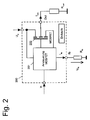
- a protected output stage often referred to as a smart-power high-side switch, as they are commercially available from International Rectifier, is in Fig. 2 shown.
- the internal structure of such an output stage 200 consists of two semiconductor chips: the actual semiconductor switch (MOSFET) 202 and a drive and Monitoring circuit 201. The two chips are arranged side by side or one above the other. Monolithic solutions (all functions on a semiconductor chip) are not widely used at high switching currents (several 10 A).
- Electrical booster heaters are used in motor vehicles, for example, for heating the indoor air, for preheating of cooling water in water-cooled engines or for heating fuel.
- Such additional heaters usually consist of numerous, combined into several heating stages heating elements and a control device.
- the heating elements are usually designed as an electrical heating resistor, in particular as a PTC element.
- a particularly advantageous PWM control can be realized in that the individual part loads are controlled out of phase in order to minimize the load on the vehicle electrical system by periodic current fluctuations.
- the frequency of the flicker of the interior lighting can be shifted to an imperceptible frequency range.
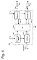
- FIG. 4 shows a conventional control device 400, in which a microcontroller ( ⁇ C) 403 is used to realize the phase-offset driving of several load circuits R Last_1 , ..., R Last_n .
- the microcontroller 403 generates the various PWM signals from any input information which is made available via an interface (eg CAN bus) 402 and controls the output stages 404-1,..., 404-n accordingly.
- the input information may include, for example, the target heat and the electrical power currently available in the electrical system.
- a disadvantage of the generation of signals for phase-offset control of several load circuits by means of a microcontroller is the comparatively large number of required components and the associated costs and space requirements.
- the development of a specific software is required for the already expensive microcontroller.
- phase-shifted driving can also be achieved for certain applications by the use of analog RC elements.
- a prerequisite here is that the input signal is a PWM signal in its temporal expression (PWM period T and duty cycle T A) can be used directly to drive the load circuits.
- FIG. 5 shows a circuit for generating the signals for phase-offset driving of several load circuits by RC elements.
- the control signal PWM is thereby delayed by (n-1) RC elements with different time constants ⁇ 2 to ⁇ n and fed to the individual output stages.
- the time constant is proportional to the product R * C.
- the respective delay time ⁇ 2 to ⁇ n is determined by the period T PWM and the number n of the load circuits.
- a disadvantage of the use of analog RC elements for generating the phase-shifted PWM signals is the high number of discrete components required and the requirements for their tolerances.
- the analogue solution with RC elements places very high demands on the accuracy of the components of the RC elements (common component tolerances are between 5% and 10%, for capacitors even higher) and the precision of the circuit in the final stage, the evaluates the analog input signal PWM in .
- a Schmitt trigger circuit is usually used, which must have extremely accurate and time-stable switching thresholds for the present application.
- a further disadvantage is that the delay times ⁇ 2 to ⁇ n must be tuned very precisely to the period duration T PWM of the PWM signal PWM in order to obtain a correct phase offset to reach the individual signals.
- the aim of the present invention is therefore to provide an improved circuit for generating the phase-shifted PWM signals.
- Another object of the present invention is to provide an integrated semiconductor switch, with which the circuit for generating the phase-shifted PWM signals can be realized inexpensively.
- an output stage for the pulse width modulated control of an electrical load.
- the output stage comprises a first input for inputting a first pulse width modulation signal, a power semiconductor switch for driving an electrical load according to the duty cycle of the first pulse width modulation signal, a delay circuit for generating a second pulse width modulation signal delayed from the first pulse width modulation signal, and a signal output for outputting the second pulse width modulation signal ,
- the delay circuit is set up such that the second pulse width modulation signal is delayed by a predetermined value from the first pulse width modulation signal, preferably by a fraction of the period duration of the first pulse width modulation signal.
- the fraction of the period is also represented by a stem break.
- the output stage according to claim 1 preferably has a second input for inputting a control signal, wherein the delay circuit is set up such that the second pulse width modulation signal is delayed from the first pulse width modulation signal by a value determined by the control signal.
- the time shift of the PWM signals can be matched to the number of stages and specified externally.
- the delay circuit comprises a first detector circuit, which determines the period duration of the first pulse width modulation signal, and generates the second pulse width modulation signal so that it is compared to the first Pulse width modulation signal is delayed by a determined by the control signal fraction of the determined period duration.
- the first detector circuit is also set up such that the period duration is determined during a period of the first pulse width modulation signal.
- the delay circuit preferably comprises a second detector circuit, which determines the duty cycle of the first pulse width modulation signal, and generates the second pulse width modulation signal such that it has the determined duty cycle.
- the second detector circuit is set up such that the switch-on duration is determined during a period of the first pulse width modulation signal.
- the phase offset can be specified directly instead of a shift time.
- the delayed PWM signal is then automatically generated with the correct timing parameters. Problems regarding the accuracy of the time base used and / or variations in the input frequency are also avoided.
- the power semiconductor switch is a MOSFET (Metal Oxide Semiconductor Field Effect Transistor).
- MOSFET Metal Oxide Semiconductor Field Effect Transistor
- the power semiconductor switch and the delay circuit is monolithically integrated on a semiconductor chip or realized on two separate semiconductor chips, which are integrated in a common housing.
- the output stage according to the invention is provided with an additional circuit for driving the power semiconductor switch.
- the drive circuit may comprise a charge pump to generate a gate voltage for driving the MOSFET, which is greater than the operating voltage.
- the additional circuit may also include a circuit for protecting the power semiconductor switch from overloading.
- the delay circuit and the additional circuit are also integrated on a common semiconductor chip. In this way, the power amplifier according to the invention can be easily manufactured and used flexibly.
- a control unit for the pulse width modulated control of an electrical load with a plurality of electrically independent load stages.
- the control unit comprises a first output stage according to the invention for driving a first load stage of the electrical load according to a predetermined first pulse width modulation signal and for outputting a second pulse width modulation signal delayed from the first pulse width modulation signal and a second output stage for driving a second load stage of the electrical load according to the second pulse width modulation signal.
- the first and the second output stage belong to a plurality of cascaded interconnected inventive output stages, which are each assigned to a load stage of the electrical load.
- each of the cascaded output stages outputs a pulse width modulation signal which is shifted from the inputted pulse width modulation signal by a fraction of the period corresponding to the number of load stages of the electrical load.
- a multi-stage load can be driven with phase-shifted PWM signals, so that the current load is evenly distributed over the PWM period. Load peaks are thus avoided as well as a simultaneous switching of several load stages.
- a method for pulse width modulated driving of an electrical load having a plurality of electrically independent stages comprises the steps of cascading a plurality of output stages according to the invention, each output stage driving one stage of the electrical load; Generating a pulse width modulation signal; and feeding the pulse width modulation signal to the first output stage of the cascaded plurality of output stages.
- FIG. 6A shows an output stage for PWM control of a load according to an embodiment of the present invention.
- the load R load Via a power semiconductor switch 602, preferably a MOSFET, the load R load is connected to the supply voltage U B.
- the load current I load is modulated by the driving circuit 601 as specified by the external PWM signal PWM in.
- the driving circuit 601 may perform additional monitoring functions and protect the power semiconductor switch 602 from being overloaded.
- the drive circuit 601 may monitor the temperature of the power semiconductor switch 602 and / or the switched current. If predetermined limit values are exceeded, the drive circuit can switch off the semiconductor switch.
- a feedback signal I lfb can be provided as a measure of the detected by a current sensor load current I load at a port Ifb for an extended external control.
- the power amplifier according to the invention is also provided with a PWM delay circuit 603, which generates a relative to the PWM input signal PWM in delayed PWM signal PWM out.
- control signal n is preferably externally specified in digital form, wherein different configurations of the control signal terminal are possible.
- the control signal connection consists of one or more digital signal line (s) to which the ratio n is applied via corresponding digital signal levels.
- any other parallel or serial interface can be used.
- control signal n can also be generated within the output stage, in particular if the output stage is implemented as an integrated component.
- the value of the control signal n may be predetermined by programming in the manufacture of the device (e.g., zener zapping) or by appropriate differential bonding between the external ports and the silicon chip.
- the output stage may also be provided with an enable input to which a digital enable signal is applied.
- the function of the block "PWM delay” 603 is activated or deactivated.
- the enable function can also be implemented as a connection or disconnection of the supply voltage U B for the circuit blocks "control MOSFET” 601 and "PWM delay” 603.
- FIG. 6B shows the structure of the PWM delay circuit 603 according to an embodiment of the present invention.
- the input signals PWM in , Enable and n are applied to a digital control unit 603b, which generates and outputs the output signal PWM out .
- the PWM delay circuit 603 further includes an internal oscillator 603a, which provides a clock signal to the digital controller 603b.
- the function of the control unit is related below Fig. 8 described in more detail.
- power amplifier 600 is preferably realized as an integrated circuit.
- the power stage according to the invention can be realized by the in the in Fig. 2 shown conventional power amplifier 200 included anyway drive and monitoring circuit 201 is extended by an additional circuit block "PWM delay".
- this circuit block will also be accommodated in the housing of the output stage and preferably also together with the block "driving MOSFET" 601 on a common semiconductor chip (see the dashed lines in FIG Fig. 6 ). In this way, the final stage of the invention can be manufactured in a particularly efficient manner.
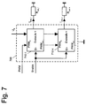
- FIG. 7 shows a control unit according to an embodiment of the present invention for driving a multi-stage load.
- the control unit 700 essentially consists of n output stages 710-1,..., 710-n according to the invention, as described above Fig. 6 have been described.
- the individual output stages 710-1,..., 710-n are connected sequentially (cascaded) so that the delayed PWM signal output by one output stage forms the input signal for the respectively next output stage.
- control unit can optionally be supplied with an enable signal which is applied equally to all output stages of the control unit.
- enable signal n which determines the amount of delay relative to the period of the PWM signal is also the same for all output stages and can be generated in the control unit itself, for example, by the associated digital inputs of the output stages are set to the corresponding logic levels.
- the PWM signal output of the last output stage 710-n is open since only (n-1) delay circuits are required to drive n load stages.
- the last output stage 710-n can therefore also be replaced by a conventional output stage without delay circuit, as shown in FIG Fig. 2 is replaced.
- FIG. 8 is a diagram based on which below the operation of the digital control unit 603b from Fig. 6B is explained.
- the digital control unit 603b can be realized by a suitable interconnection of conventional logic gates.
- the period T PWM and the duty cycle T Ein can be determined, for example, by means of a driven by the oscillator 603a binary counter and stored in a latch become.
- the control unit preferably has a further register in which the delay T v calculated on the basis of the determined period duration and the control signal n is stored.
- the output signal PWM out can also be generated by means of a binary counter driven by the oscillator and a comparator which compares the counter reading with the stored register values.
- the measurement of the input signal is repeated every PWM period. For this reason, no provision is made for stabilizing the oscillator frequency against (thermal) drift, since drift-induced changes in the oscillator frequency occur on a time scale which is significantly slower than the period duration of the pulse width modulation.
- the tuning of the delay time to the period of the pulse width modulation is unnecessary, since the output stage according to the invention requires as input information only the number of stages to be controlled in phase and from this the required delay time as a function of the measured Period duration calculated by yourself. In this way, the control unit according to the invention can even respond to variations in the frequency of the external PWM signal.
- a digital switching mechanism is used to generate the delayed PWM signal PWM out .
- the present invention is not limited to digital generation of the delayed PWM signal PWM out . Rather, an analog circuit, for example, with a PLL (phase locked loop: phase locked loop) can be used.
- PLL phase locked loop: phase locked loop
- FIG. 9 shows the construction of a final stage according to an alternative embodiment of the present invention.
- the power amp off Fig. 9 differs only so far from the power amplifier Fig. 6A when the drive circuit 601 is driven by the delayed PWM signal PWM out and not by the PWM input signal PWM in . Otherwise, those in the FIGS. 6A and 9 denoted by the same reference numerals elements the same function, the detailed description of which can be omitted here.
- the output stage according to the invention can be realized by the delay circuit together is integrated with the actual power semiconductor switch and an associated monitoring and control circuit in a single block.
- a control unit for phase-shifted PWM control can be realized in a simple manner, which is independent of an exact time base.
Abstract
Description
Die vorliegende Erfindung bezieht sich auf einen Halbleiterschalter mit integrierter Verzögerungsschaltung, eine Steuereinheit zur pulsweitenmodulierten Ansteuerung einer mehrstufigen elektrischen Last sowie ein entsprechendes Verfahren.The present invention relates to a semiconductor switch with integrated delay circuit, a control unit for the pulse width modulated control of a multi-stage electrical load and a corresponding method.
Die Steuerung der Strom- bzw. Leistungsaufnahme einer elektrischen Last, wie zum Beispiel elektrischer Heizungen, Glühlampen, Gleichstrommotoren, etc., kann herkömmlich über eine Pulsweitenmodulation (PWM) erfolgen. Die Versorgungsspannung wird dabei in periodischen Abständen ein- und ausgeschaltet. Über das Tastverhältnis, also das Verhältnis der Einschaltdauer TEin innerhalb einer Periode zur Dauer TPWM der Periode (vgl.
Als End- oder Schaltstufen einer PWM-Steuerung, d.h. als Halbleiterschalter für hohe Ströme, werden vorzugsweise MOSFETs eingesetzt, die entweder durch ihre äußere Zusatzbeschaltung angesteuert und gegen Überlastung (Überstrom, Überspannung und Übertemperatur) geschützt werden oder die diese erforderliche Zusatzbeschaltung bereits in ihrem Gehäuse beinhalten. Eine derartig geschützte Endstufe, oft auch als Smart-Power-Highside-Switch bezeichnet, wie sie beispielsweise von International Rectifier kommerziell erhältlich sind, ist in
Nachteilig an einer PWM-Ansteuerung von Hochstromverbrauchem, insbesondere von Hochstromverbrauchern in einem Kfz-Bordnetz, wie z.B. einer elektrischen Zusatzheizung oder den Glühkerzen eines Dieselmotors, sind die durch die Taktung auftretenden Belastungsspitzen, die sich beispielsweise durch ein störendes Flimmern der Innenraumbeleuchtung bemerkbar machen können, sowie die generell mit den Schaltvorgängen verbundene EMV-Problematik (EMV: elektromagnetische Verträglichkeit).A disadvantage of a PWM control of Hochstromverbrauchem, especially of high current loads in a vehicle electrical system, such. an electric auxiliary heater or the glow plugs of a diesel engine, the peak loads occurring due to the timing, which can be noticeable for example by a disturbing flicker of the interior lighting, and the generally associated with the switching operations EMC problems (EMC: electromagnetic compatibility).
Aus der europäischen Patentschrift
Elektrische Zusatzheizungen werden in Kraftfahrzeugen beispielsweise zur Erwärmung der Innenraumluft, zur Vorheizung von Kühlwasser bei wassergekühlten Motoren oder zur Erwärmung von Kraftstoff verwendet. Derartige Zusatzheizungen bestehen üblicherweise aus zahlreichen, zu mehreren Heizstufen zusammengefassten Heizelementen und einer Steuervorrichtung. Die Heizelemente sind in der Regel als elektrischer Heizwiderstand, insbesondere als PTC-Element ausgebildet.Electrical booster heaters are used in motor vehicles, for example, for heating the indoor air, for preheating of cooling water in water-cooled engines or for heating fuel. Such additional heaters usually consist of numerous, combined into several heating stages heating elements and a control device. The heating elements are usually designed as an electrical heating resistor, in particular as a PTC element.
Eine besonders vorteilhafte PWM-Ansteuerung kann dadurch realisiert werden, dass die einzelnen Teillasten phasenversetzt angesteuert werden, um die Belastung des Kfz-Bordnetz durch periodische Stromschwankungen minimal zu halten. Wie in
Nachteilig an der Erzeugung der Signale zur phasenversetzten Ansteuerung mehrerer Lastkreise mittels eines Mikrocontrollers ist die vergleichsweise große Zahl erforderlicher Bauteile sowie die damit einhergehenden Kosten und der Platzbedarf. Zudem ist für den an sich schon kostspieligen Mikrocontroller die Entwicklung einer spezifischen Software erforderlich.A disadvantage of the generation of signals for phase-offset control of several load circuits by means of a microcontroller is the comparatively large number of required components and the associated costs and space requirements. In addition, the development of a specific software is required for the already expensive microcontroller.
Eine besonders einfache Lösung zum phasenversetzten Ansteuern lässt sich für gewisse Anwendungen auch durch den Einsatz von analogen RC-Gliedern erreichen. Eine Voraussetzung hierbei ist, dass das Eingangssignal ein PWM-Signal ist, das in seiner zeitlichen Ausprägung (Periodendauer TPWM und Einschaltdauer TEin) direkt zur Ansteuerung der Lastkreise verwendet werden kann.A particularly simple solution for phase-shifted driving can also be achieved for certain applications by the use of analog RC elements. A prerequisite here is that the input signal is a PWM signal in its temporal expression (PWM period T and duty cycle T A) can be used directly to drive the load circuits.

Nachteilig an der Verwendung analoger RC-Glieder zur Erzeugung der phasenversetzten PWM-Signale ist die hohe Zahl der erforderlichen diskreten Bausteine sowie die Anforderungen an deren Toleranzen. Die analoge Lösung mit RC-Gliedern stellt sehr hohe Anforderungen an die Genauigkeit der Bauteile der RC-Glieder (übliche Bauteile-Toleranzen liegen zwischen 5% und 10%, bei Kondensatoren auch noch darüber) und an die Präzision der Schaltung in der Endstufe, die das analoge Eingangssignal PWMin auswertet. Für diese Schaltung wird üblicherweise eine Schmitt-Trigger-Schaltung eingesetzt, die für die vorliegende Anwendung äußerst genaue und zeitlich stabile Schaltschwellen aufweisen muss. Ein weiterer Nachteile ist, dass die Verzögerungszeiten τ2 bis τn sehr genau auf die Periodendauer TPWM des PWM-Signals PWM abgestimmt sein müssen, um einen korrekten Phasenversatz der einzelnen Signale zu erreichen. Umgekehrt ergeben sich aus der Verkoppelung von Periodendauer und Verzögerungszeit entsprechende Anforderungen an das Steuergerät, das das PWM-Signal erzeugt. Die Frequenz des PWM-Signals muss auch dort sehr genau und stabil (ohne Drift) eingehalten werden. Derartige Forderungen an PWM-Signale sind aber nur mit entsprechend hohem Schaltungsaufwand zu realisieren. In einer PWM-Regelung wird zudem nicht die Frequenz des PWM-Signals ausgewertet, sondern nur das Tastverhältnis. Frequenzabweichungen sollten daher zulässig sein.A disadvantage of the use of analog RC elements for generating the phase-shifted PWM signals is the high number of discrete components required and the requirements for their tolerances. The analogue solution with RC elements places very high demands on the accuracy of the components of the RC elements (common component tolerances are between 5% and 10%, for capacitors even higher) and the precision of the circuit in the final stage, the evaluates the analog input signal PWM in . For this circuit, a Schmitt trigger circuit is usually used, which must have extremely accurate and time-stable switching thresholds for the present application. A further disadvantage is that the delay times τ 2 to τ n must be tuned very precisely to the period duration T PWM of the PWM signal PWM in order to obtain a correct phase offset to reach the individual signals. Conversely, the coupling of period duration and delay time results in corresponding demands on the control unit which generates the PWM signal. The frequency of the PWM signal must be kept there very accurately and stable (without drift). Such demands on PWM signals can only be realized with correspondingly high circuit complexity. In addition, in a PWM control, the frequency of the PWM signal is not evaluated, but only the duty cycle. Frequency deviations should therefore be allowed.
Ziel der vorliegenden Erfindung ist es daher, eine verbesserte Schaltung zur Erzeugung der phasenversetzten PWM-Signale anzugeben. Ein weiteres Ziel der vorliegenden Erfindung ist es, einen integrierten Halbleiterschalter anzugeben, mit dem die Schaltung zur Erzeugung der phasenversetzten PWM-Signale kostengünstig realisiert werden kann. Außerdem ist es ein Ziel der vorliegende Erfindung, ein Steuergerät und ein entsprechendes Verfahren anzugeben, mit dem eine verbesserte PWM-Ansteuerung einer mehrstufigen elektrischen Last ermöglicht wird.The aim of the present invention is therefore to provide an improved circuit for generating the phase-shifted PWM signals. Another object of the present invention is to provide an integrated semiconductor switch, with which the circuit for generating the phase-shifted PWM signals can be realized inexpensively. In addition, it is an object of the present invention to provide a control device and a corresponding method, with which an improved PWM control of a multi-stage electrical load is made possible.
Dies wird durch die Merkmale der unabhängigen Ansprüche erreicht. Bevorzugte Ausführungsformen sind Gegenstand der abhängigen Ansprüche.This is achieved by the features of the independent claims. Preferred embodiments are subject of the dependent claims.
Es ist der besondere Ansatz der vorliegenden Erfindung, eine Endstufe zur PWM-Ansteuerung einer Laststufe mit einer Verzögerungsschaltung zu versehen, die zusätzlich zu dem durch ein PWM-Eingangssignal modulierten Laststrom ein PWM-Ausgangssignal liefert, das gegenüber dem PWM-Eingangssignal um einen vorgegebenen Bruchteil der Periodendauer verzögert ist.It is the particular approach of the present invention to provide an output stage for PWM driving a load stage with a delay circuit which, in addition to the load current modulated by a PWM input signal, provides a PWM output signal opposite the PWM input signal by a predetermined fraction the period is delayed.
Gemäß einem ersten Aspekt der vorliegenden Erfindung wird eine Endstufe zur pulsweitenmodulierten Ansteuerung einer elektrischen Last zur Verfügung gestellt. Die Endstufe umfasst einen ersten Eingang zur Eingabe eines ersten Pulsweitenmodulationssignals, einen Leistungshalbleiterschalter zur Ansteuerung einer elektrischen Last gemäß dem Tastverhältnis des ersten Pulsweitenmodulationssignals, eine Verzögerungsschaltung zur Erzeugung eines zweiten Pulsweitenmodulationssignals, das gegenüber dem ersten Pulsweitenmodulationssignal verzögert ist, und einen Signalausgang zur Ausgabe des zweiten Pulsweitenmodulationssignals.According to a first aspect of the present invention, an output stage is provided for the pulse width modulated control of an electrical load. The output stage comprises a first input for inputting a first pulse width modulation signal, a power semiconductor switch for driving an electrical load according to the duty cycle of the first pulse width modulation signal, a delay circuit for generating a second pulse width modulation signal delayed from the first pulse width modulation signal, and a signal output for outputting the second pulse width modulation signal ,
Vorteilhafterweise ist die Verzögerungsschaltung so eingerichtet, dass das zweite Pulsweitenmodulationssignal gegenüber dem ersten Pulsweitenmodulationssignal um einen vorbestimmten Wert verzögert ist, vorzugsweise um einem Bruchteil der Periodendauer des ersten Pulsweitenmodulationssignals. Auf diese Weise können mehrere Stufen einer elektrischen Last in einfacher Weise mit PWM-Signalen angesteuert werden, die einen festen Zeit- oder Phasenversatz aufweisen. Vorzugsweise ist der Bruchteil der Periodendauer außerdem durch einen Stammbruch darstellbar. Durch eine Kaskadierung der Verzögerungsschaltungen können dann alle erforderlichen Phasenverschiebungen zur Ansteuerung einer mehrstufigen Last erzeugt werden.Advantageously, the delay circuit is set up such that the second pulse width modulation signal is delayed by a predetermined value from the first pulse width modulation signal, preferably by a fraction of the period duration of the first pulse width modulation signal. In this way, multiple stages of an electrical load can be easily controlled with PWM signals having a fixed time or phase offset. Preferably, the fraction of the period is also represented by a stem break. By cascading the delay circuits, all required phase shifts can then be generated to drive a multi-stage load.
Vorzugsweise besitzt die Endstufe nach Anspruch 1 einen zweiten Eingang zur Eingabe eines Steuersignals, wobei die Verzögerungsschaltung so eingerichtet ist, dass das zweite Pulsweitenmodulationssignal gegenüber dem ersten Pulsweitenmodulationssignal um einen durch das Steuersignal bestimmten Wert verzögert ist. Damit kann der zeitliche Verschiebung der PWM-Signale auf die Anzahl der Stufen abgestimmt und extern vorgegeben werden.The output stage according to
Vorzugsweise umfasst die Verzögerungsschaltung eine erste Detektorschaltung, die die Periodendauer des ersten Pulsweitenmodulationssignals ermittelt, und das zweite Pulsweitenmodulationssignal so erzeugt, dass es gegenüber dem ersten Pulsweitenmodulationssignal um einen durch das Steuersignal bestimmten Bruchteil der ermittelten Periodendauer verzögert ist. Vorzugsweise ist die erste Detektorschaltung auch so eingerichtet, dass die Periodendauer während einer Periode des ersten Pulsweitenmodulationssignals ermittelt wird. Desweiteren umfasst die Verzögerungsschaltung vorzugsweise eine zweite Detektorschaltung, die die Einschaltdauer des ersten Pulsweitenmodulationssignals ermittelt, und das zweite Pulsweitenmodulationssignal so erzeugt, dass es die ermittelte Einschaltdauer aufweist. Vorteilhafterweise ist die zweite Detektorschaltung so eingerichtet, dass die Einschaltdauer während einer Periode des ersten Pulsweitenmodulationssignals ermittelt wird. Dadurch kann anstelle einer Verschiebungszeit direkt der Phasenversatz angegeben werden. Das verzögerte PWM-Signal wird dann automatisch mit den richtigen Timing-Parametem erzeugt. Probleme hinsichtlich der Genauigkeit der verwendeten Zeitbasis und/oder Schwankungen in der Eingangsfrequenz werden ebenfalls vermieden.Preferably, the delay circuit comprises a first detector circuit, which determines the period duration of the first pulse width modulation signal, and generates the second pulse width modulation signal so that it is compared to the first Pulse width modulation signal is delayed by a determined by the control signal fraction of the determined period duration. Preferably, the first detector circuit is also set up such that the period duration is determined during a period of the first pulse width modulation signal. Furthermore, the delay circuit preferably comprises a second detector circuit, which determines the duty cycle of the first pulse width modulation signal, and generates the second pulse width modulation signal such that it has the determined duty cycle. Advantageously, the second detector circuit is set up such that the switch-on duration is determined during a period of the first pulse width modulation signal. As a result, the phase offset can be specified directly instead of a shift time. The delayed PWM signal is then automatically generated with the correct timing parameters. Problems regarding the accuracy of the time base used and / or variations in the input frequency are also avoided.
Vorzugsweise ist der Leistungshalbleiterschalter ein MOSFET (Metal Oxide Semiconductor Field Effect Transistor). Derartige Leistungshalbleiterschalter zeichnen sich durch ihre hervorragenden Fertigungs- und Schalteigenschaften aus.Preferably, the power semiconductor switch is a MOSFET (Metal Oxide Semiconductor Field Effect Transistor). Such power semiconductor switches are characterized by their excellent manufacturing and switching properties.
Vorzugsweise ist der Leistungshalbleiterschalter und die Verzögerungsschaltung monolithisch auf einem Halbleiterchip integriert oder auf zwei getrennten Halbleiterchips realisiert, die in einem gemeinsamen Gehäuse integriert sind. Vorzugsweise ist die erfindungsgemäße Endstufe mit einer Zusatzschaltung zur Ansteuerung des Leistungshalbleiterschalters versehen. Die Ansteuerschaltung kann insbesondere eine Ladungspumpe umfassen, um eine Gate-Spannung zur Ansteuerung des MOSFETs zu erzeugen, die größer ist als die Betriebsspannung. Die Zusatzschaltung kann auch eine Schaltung zum Schutz des Leistungshalbleiterschalters vor Überlastung umfassen. Vorteilhafterweise sind die Verzögerungsschaltung und die Zusatzschaltung auch auf einem gemeinsamen Halbleiterchip integriert. Auf diese Weise lässt sich die erfindungsgemäße Endstufe leicht fertigen und flexibel einsetzen.Preferably, the power semiconductor switch and the delay circuit is monolithically integrated on a semiconductor chip or realized on two separate semiconductor chips, which are integrated in a common housing. Preferably, the output stage according to the invention is provided with an additional circuit for driving the power semiconductor switch. In particular, the drive circuit may comprise a charge pump to generate a gate voltage for driving the MOSFET, which is greater than the operating voltage. The additional circuit may also include a circuit for protecting the power semiconductor switch from overloading. Advantageously, the delay circuit and the additional circuit are also integrated on a common semiconductor chip. In this way, the power amplifier according to the invention can be easily manufactured and used flexibly.
Gemäß einem zweiten Aspekt der vorliegenden Erfindung wird eine Steuereinheit zur pulsweitenmodulierten Ansteuerung einer elektrischen Last mit einer Mehrzahl elektrisch unabhängiger Laststufen zur Verfügung gestellt. Die Steuereinheit umfasst eine erste erfindungsgemäße Endstufe zur Ansteuerung einer ersten Laststufe der elektrischen Last gemäß einem vorgegebenen ersten Pulsweitenmodulationssignal und zur Ausgabe eines gegenüber dem ersten Pulsweitenmodulationssignal verzögerten zweiten Pulsweitenmodulationssignals und eine zweite Endstufe zur Ansteuerung einer zweiten Laststufe der elektrischen Last gemäß dem zweiten Pulsweitenmodulationssignal.According to a second aspect of the present invention, a control unit is provided for the pulse width modulated control of an electrical load with a plurality of electrically independent load stages. The control unit comprises a first output stage according to the invention for driving a first load stage of the electrical load according to a predetermined first pulse width modulation signal and for outputting a second pulse width modulation signal delayed from the first pulse width modulation signal and a second output stage for driving a second load stage of the electrical load according to the second pulse width modulation signal.
Vorzugsweise gehört die erste und die zweite Endstufe zu einer Mehrzahl kaskadiert verschalteter erfindungsgemäßer Endstufen, die jeweils einer Laststufe der elektrischen Last zugeordnet sind. Vorteilhafterweise gibt jede der kaskadiert verschalteten Endstufen ein Pulsweitenmodulationssignal aus, das gegenüber dem eingegebenen Pulsweitenmodulationssignal um einen Bruchteil der Periodendauer verschoben ist, der der Anzahl der Laststufen der elektrischen Last entspricht. Auf diese Weise kann eine mehrstufige Last mit phasenversetzten PWM-Signalen angesteuert werden, so dass die Strombelastung gleichmäßig über die PWM-Periodendauer verteilt ist. Lastspitzen werden so ebenso vermieden, wie eine gleichzeitige Schaltung mehrerer Laststufen.Preferably, the first and the second output stage belong to a plurality of cascaded interconnected inventive output stages, which are each assigned to a load stage of the electrical load. Advantageously, each of the cascaded output stages outputs a pulse width modulation signal which is shifted from the inputted pulse width modulation signal by a fraction of the period corresponding to the number of load stages of the electrical load. In this way, a multi-stage load can be driven with phase-shifted PWM signals, so that the current load is evenly distributed over the PWM period. Load peaks are thus avoided as well as a simultaneous switching of several load stages.
Gemäß einem dritten Aspekt der vorliegenden Erfindung wird ein Verfahren zur pulsweitenmodulierten Ansteuerung einer elektrischen Last mit einer Mehrzahl elektrisch unabhängiger Stufen zur Verfügung gestellt. Das Verfahren umfasst die Schritte Kaskadieren einer Mehrzahl von erfindungsgemäßen Endstufen, wobei jede Endstufe eine Stufe der elektrischen Last ansteuert; Erzeugen eines Pulsweitenmodulationssignals; und Einspeisen des Pulsweitenmodulationssignals an der ersten Endstufe der kaskadierten Mehrzahl von Endstufen.According to a third aspect of the present invention, there is provided a method for pulse width modulated driving of an electrical load having a plurality of electrically independent stages. The method comprises the steps of cascading a plurality of output stages according to the invention, each output stage driving one stage of the electrical load; Generating a pulse width modulation signal; and feeding the pulse width modulation signal to the first output stage of the cascaded plurality of output stages.
Die Erfindung wird im folgenden unter Bezugnahme auf die beigefügten Abbildungen beschrieben, in denen:
- Fig. 1
- eine schematische Darstellung der Pulsweitenmodulation zeigt,
- Fig. 2
- eine schematische Darstellung einer herkömmlichen Endstufe zeigt,
- Fig. 3
- eine schematische Darstellung der Signale zur phasenversetzten PWM-Ansteuerung einer mehrstufigen Last zeigt,
- Fig. 4
- schematisch eine herkömmliche Schaltung zur Erzeugung der phasenversetzten Signale durch einen Mikrocontroller darstellt,
- Fig. 5
- schematisch eine herkömmliche Schaltung zur Erzeugung der phasenversetzten Signale durch RC-Glieder darstellt,
- Fig. 6A
- schematisch den Aufbau einer PWM-Endstufe gemäß einer Ausführungsform der vorliegenden Erfindung darstellt,
- Fig. 6B
- schematisch den Aufbau der PWM-Verzögerungsschaltung der PWM-Endstufe aus
Fig. 6A gemäß einer Ausführungsform der vorliegenden Erfindung darstellt, - Fig. 7
- schematisch den Aufbau einer Steuereinheit zur pulsweitenmodulierten Ansteuerung einer mehrstufigen elektrischen Last gemäß einer Ausführungsform der vorliegenden Erfindung darstellt,
- Fig. 8
- die Erzeugung des verzögerten PWM-Signals durch die erfindungsgemäße PWM-Verzögerungsschaltung erläutert, und
- Fig. 9
- schematisch den Aufbau eines integrierten Halbleiterschalters gemäß einer weiteren Ausführungsform der vorliegenden Erfindung darstellt.
- Fig. 1
- shows a schematic representation of the pulse width modulation,
- Fig. 2
- a schematic representation of a conventional power amplifier shows
- Fig. 3
- shows a schematic representation of the signals for phase-offset PWM control of a multi-stage load,
- Fig. 4
- schematically illustrates a conventional circuit for generating the phase-shifted signals by a microcontroller,
- Fig. 5
- schematically illustrates a conventional circuit for generating the phase-shifted signals by RC elements,
- Fig. 6A
- schematically illustrates the structure of a PWM output stage according to an embodiment of the present invention,
- Fig. 6B
- schematically shows the structure of the PWM delay circuit of the PWM output stage
Fig. 6A according to an embodiment of the present invention, - Fig. 7
- schematically illustrates the structure of a control unit for the pulse width modulated control of a multi-stage electrical load according to an embodiment of the present invention,
- Fig. 8
- explains the generation of the delayed PWM signal by the PWM delay circuit according to the invention, and
- Fig. 9
- schematically illustrates the structure of a semiconductor integrated switch according to another embodiment of the present invention.
Die erfindungsgemäße Endstufe ist außerdem mit einer PWM-Verzögerungsschaltung 603 versehen, die ein gegenüber dem PWM-Eingangssignal PWMin verzögertes PWM-Signal PWMout erzeugt. Die Verzögerungsdauer Tv bemisst sich dabei aus der Periodendauer TPWM des PWM-Eingangssignals PWMin und einem Steuersignal n: ![]()
wobei n vorzugsweise eine ganze Zahl größer 1, insbesondere n=2, 3, 4, 5, 6 oder 8, darstellt. Das Verhältnis der Verzögerungsdauer Tv zur Periodendauer TPWM ist somit durch einen Stammbruch (d. h. einen Bruch mit Zähler=1) darstellbar.The power amplifier according to the invention is also provided with a ![]()
where n is preferably an integer greater than 1, in particular n = 2, 3, 4, 5, 6 or 8. The ratio of the delay time T v to the period T PWM is thus represented by a parent break (ie a break with counter = 1).
Das Steuersignal n wird dabei bevorzugt in digitaler Form extern vorgegeben, wobei unterschiedliche Ausgestaltungen des Steuersignalanschlusses möglich sind. Im einfachsten Falle besteht der Steuersignalanschluss aus einer oder mehreren digitalen Signalleitung(en), an denen das Teilverhältnis n über entsprechende digitale Signalpegel angelegt wird. Alternativ kann aber auch jede andere parallele oder serielle Schnittstelle verwendet werden.The control signal n is preferably externally specified in digital form, wherein different configurations of the control signal terminal are possible. In the simplest case, the control signal connection consists of one or more digital signal line (s) to which the ratio n is applied via corresponding digital signal levels. Alternatively, however, any other parallel or serial interface can be used.
Das Steuersignal n kann aber auch innerhalb der Endstufe erzeugt werden, insbesondere wenn die Endstufe als integrierter Baustein realisiert wird. Der Wert des Steuersignals n kann dabei durch eine Programmierung bei der Herstellung des Bausteines (z.B. Zener-Zapping) oder durch geeignete unterschiedliche Bondverbindungen zwischen den externen Anschlüssen und dem Silizium-Chip vorgegeben werden.However, the control signal n can also be generated within the output stage, in particular if the output stage is implemented as an integrated component. The value of the control signal n may be predetermined by programming in the manufacture of the device (e.g., zener zapping) or by appropriate differential bonding between the external ports and the silicon chip.
Die Endstufe kann außerdem mit einem "Enable"-Eingang versehen sein, an den ein digitales Enable-Signal angelegt wird. Mit dem Eingangssignal Enable wird die Funktion des Blockes "PWM-Verzögerung" 603 aktiviert bzw. deaktiviert. Die Enable-Funktion kann auch als Zu- bzw. Wegschalten der Versorgungsspannung UB für die Schaltungsblöcke "Ansteuerung MOSFET" 601 und "PWM-Verzögerung" 603 realisiert werden.The output stage may also be provided with an enable input to which a digital enable signal is applied. With the input signal Enable, the function of the block "PWM delay" 603 is activated or deactivated. The enable function can also be implemented as a connection or disconnection of the supply voltage U B for the circuit blocks "control MOSFET" 601 and "PWM delay" 603.
Die in
Neben dem externen PWM-Signal kann die Steuereinheit optional mit einem Enable-Signal versorgt werden, das an alle Endstufen der Steuereinheit gleichermaßen angelegt wird. Das (in
In der Steuereinheit aus
Innerhalb jeder PWM-Periode TPWM wird einerseits das PWM-Eingangssignal PWMin vermessen und andererseits das PWM-Ausgangssignal gemäß der Ergebnisse der Vermessung aus der vorhergehenden Periode generiert. Im einzelnen werden die folgenden Schritte durch das Steuerwerk durchgeführt:
- (1) Vermessen des PWM-Eingangssignals PWMin (mit der Periodendauer TPWM und der Einschaltdauer TEin ) hinsichtlich TPWM und TEin und speichern der Werte,
- (2) Ermitteln der vom Steuersignal n, bzw. von der Anzahl n der Lastkreise abhängigen Verzögerungszeit Tv, mit der das PWM-Eingangssignal am Ausgang PWMout ausgegeben werden soll: Tv = TPWM / n,
- (3) nach Ablauf eines Taktzyklus TPWM des Signals PWMin Start der Verzögerungszeit Tv, und
- (4) nach Ablauf der Verzögerungszeit Tv Aktivierung des Ausgangssignals PWMout für die Zeit TEin.
- (1) measurement of the PWM input signal PWM in (with the period T and the PWM duty cycle T A) with respect to T and T PWM A and store the values,
- (2) determining the delay time T v , which is dependent on the control signal n, or on the number n of load circuits, with which the PWM input signal is to be output at the output PWM out : T v = T PWM / n,
- (3) after a clock cycle T PWM of the signal PWM in the start of the delay time T v , and
- (4) v after the delay time T activation of the output signal PWM out for the time T A.
Das digitale Steuerwerk 603b kann durch eine geeignete Verschaltung herkömmlicher Logikgatter realisiert werden. Die Periodendauer TPWM und die Einschaltdauer TEin können beispielsweise mit Hilfe von einem durch den Oszillator 603a getriebenen Binärzähler ermittelt werden und in einem Auffangregister gespeichert werden. Vorzugsweise besitzt das Steuerwerk ein weiteres Register, in dem die auf Basis der ermittelten Periodendauer und des Steuersignals n berechnete Verzögerung Tv gespeichert wird. Das Ausgangssignal PWMout kann ebenfalls mittels eines durch den Oszillator getriebenen Binärzählers und eines Komparators, der den Zählerstand mit den gespeicherten Registerwerten vergleicht, erzeugt werden.The
Sowohl die Vermessung des Eingangssignals PWMin, als auch die Erzeugung des Ausgangssignals PWMout erfolgt relativ zu dem von dem Oszillator 603a erzeugten Taktsignal. Auf diese Weise werden die Probleme hinsichtlich der Genauigkeit und der Stabilität der Zeitbasis in herkömmlichen Steuereinheiten zur phasenversetzten Ansteuerung mehrerer Lastkreise gelöst. Insbesondere ist keine Eichung der Zeitbasis (beispielsweise in Millisekunden oder dergleichen) erforderlich, da der genaue Wert der Taktfrequenz des Oszillators 603a keine Rolle für die Erzeugung des Ausgangssignals spielt. Allenfalls die Granularität in der Bestimmung der Verzögerungsdauer Tv und der Einschaltdauer TEin hängt von der Wahl der Taktfrequenz ab. In der Praxis werden PWM-Signale mit einer Frequenz von einigen 10Hz bis 1 kHz verwendet, so dass Taktfrequenzen von 10kHz-1 MHz für eine ausreichende zeitliche Auflösung hinreichend sind.Both the measurement of the input signal PWM in and the generation of the output signal PWM out occur relative to the clock signal generated by the
Zum anderen wird die Vermessung des Eingangssignals in jeder PWM-Periode wiederholt. Aus diesem Grund sind keine Vorkehrungen zur Stabilisierung der Oszillatorfrequenz gegen (thermische) Drift erforderlich, da driftbedingte Änderungen der Oszillatorfrequenz auf einer Zeitskala auftreten, die deutlich langsamer ist, als die Periodendauer der Pulsweitenmodulation.On the other hand, the measurement of the input signal is repeated every PWM period. For this reason, no provision is made for stabilizing the oscillator frequency against (thermal) drift, since drift-induced changes in the oscillator frequency occur on a time scale which is significantly slower than the period duration of the pulse width modulation.
Schließlich erübrigt sich auch die Abstimmung der Verzögerungszeit auf die Periodendauer der Pulsweitenmodulation, da die erfindungsgemäße Endstufe als Eingabeinformation lediglich die Anzahl der phasenversetzt anzusteuernden Stufen benötigt und daraus die erforderliche Verzögerungszeit in Abhängigkeit von der gemessenen Periodendauer selbst berechnet. Auf diese Weise kann die erfindungsgemäße Steuereinheit sogar auf Variationen in der Frequenz des externen PWM-Signals reagieren.Finally, the tuning of the delay time to the period of the pulse width modulation is unnecessary, since the output stage according to the invention requires as input information only the number of stages to be controlled in phase and from this the required delay time as a function of the measured Period duration calculated by yourself. In this way, the control unit according to the invention can even respond to variations in the frequency of the external PWM signal.
In den oben beschriebenen Ausführungsformen der erfindungsgemäßen PWM-Endstufe wird ein digitales Schaltwerk zur Erzeugung des verzögerten PWM-Signals PWMout verwendet. Die vorliegende Erfindung ist aber nicht auf eine digitale Erzeugung des verzögerten PWM-Signals PWMout beschränkt. Vielmehr kann auch eine analoge Schaltung, beispielsweise mit einem PLL (phase locked loop: Phasenregelkreis) verwendet werden.In the embodiments of the PWM output stage according to the invention described above, a digital switching mechanism is used to generate the delayed PWM signal PWM out . However, the present invention is not limited to digital generation of the delayed PWM signal PWM out . Rather, an analog circuit, for example, with a PLL (phase locked loop: phase locked loop) can be used.
Zusammenfassend kann festgestellt werden, dass zur Ansteuerung einer mehrstufigen Last mit Pulsweitenmodulation (PWM) üblicherweise die einzelnen Stufen getrennt mit jeweils phasenversetzt getakteten Lastströmen beaufschlagt werden, um Lastspitzen zu vermeiden. Herkömmliche Steuereinheiten zur phasenversetzten PWM-Ansteuerung zeichnen sich durch hohe Komplexität und/oder Probleme mit der zeitlichen Präzision der Taktung der einzelnen Lastströme aus. Es ist daher der besondere Ansatz der vorliegenden Erfindung, eine Endstufe zur PWM-Ansteuerung einer Laststufe mit einer Verzögerungsschaltung zu versehen, die zusätzlich zu dem durch ein PWM-Eingangssignal modulierten Laststrom ein PWM-Ausgangssignal liefert, das gegenüber dem PWM-Eingangssignal um einen vorgegebenen Bruchteil der Periodendauer verzögert ist. Insbesondere kann die erfindungsgemäße Endstufe realisiert werden, indem die Verzögerungsschaltung zusammen mit dem eigentlichen Leistungshalbleiterschalter und einer zugehörigen Überwachungs- und Ansteuerschaltung in einem einzigen Baustein integriert wird. Durch eine Kaskadierung derartiger Endstufen kann auf einfache Weise eine Steuereinheit zur phasenversetzten PWM-Ansteuerung realisiert werden, die unabhängig ist von einer genauen Zeitbasis.In summary, it can be stated that in order to control a multistage load with pulse width modulation (PWM), the individual stages are usually applied separately with phase-switched, clocked load currents in order to avoid load peaks. Conventional control units for phase-shifted PWM control are characterized by high complexity and / or problems with the temporal precision of the timing of the individual load currents. It is therefore the particular approach of the present invention to provide an output stage for PWM driving a load stage with a delay circuit which, in addition to the load current modulated by a PWM input signal, provides a PWM output signal which is one preset from the PWM input signal Fraction of the period is delayed. In particular, the output stage according to the invention can be realized by the delay circuit together is integrated with the actual power semiconductor switch and an associated monitoring and control circuit in a single block. By cascading such output stages, a control unit for phase-shifted PWM control can be realized in a simple manner, which is independent of an exact time base.
Claims (23)
eine Verzögerungsschaltung (603) zur Erzeugung eines zweiten Pulsweitenmodulationssignals, das gegenüber dem ersten Pulsweitenmodulationssignal verzögert ist, und
einen Signalausgang (613) zur Ausgabe des zweiten Pulsweitenmodulationssignals.Amplifier for the pulse width modulated control of an electrical load, wherein the output stage comprises:
a delay circuit (603) for generating a second pulse width modulation signal delayed from the first pulse width modulation signal, and
a signal output (613) for outputting the second pulse width modulation signal.
Kaskadieren einer Mehrzahl von Endstufen nach einem der Ansprüche 1 bis 16, wobei jede Endstufe eine Stufe der elektrischen Last ansteuert;
Erzeugen eines Pulsweitenmodulationssignals; und
Einspeisen des Pulsweitenmodulationssignals an der ersten Endstufe der kaskadierten Mehrzahl von Endstufen.Method for the pulse width modulated control of an electrical load with a plurality of electrically independent stages with the steps
Cascading a plurality of power amplifiers according to any one of claims 1 to 16, wherein each power stage drives one stage of the electrical load;
Generating a pulse width modulation signal; and
Feeding the pulse width modulation signal to the first output stage of the cascaded plurality of output stages.
Priority Applications (5)
| Application Number | Priority Date | Filing Date | Title |
|---|---|---|---|
| EP07008356A EP1986322B1 (en) | 2007-04-24 | 2007-04-24 | Semiconductor switch with integrated delay circuit |
| JP2008107867A JP2008271554A (en) | 2007-04-24 | 2008-04-17 | Semiconductor switch with integrated delay circuit |
| CNA2008100950013A CN101295929A (en) | 2007-04-24 | 2008-04-21 | Semiconductor switch with integrated delay circuit |
| US12/107,322 US20080266016A1 (en) | 2007-04-24 | 2008-04-22 | Semiconductor Switch with Integrated Delay Circuit |
| KR1020080038178A KR20080095804A (en) | 2007-04-24 | 2008-04-24 | Semiconductor switch with integrated delay circuit |
Applications Claiming Priority (1)
| Application Number | Priority Date | Filing Date | Title |
|---|---|---|---|
| EP07008356A EP1986322B1 (en) | 2007-04-24 | 2007-04-24 | Semiconductor switch with integrated delay circuit |
Publications (2)
| Publication Number | Publication Date |
|---|---|
| EP1986322A1 true EP1986322A1 (en) | 2008-10-29 |
| EP1986322B1 EP1986322B1 (en) | 2012-11-14 |
Family
ID=38137492
Family Applications (1)
| Application Number | Title | Priority Date | Filing Date |
|---|---|---|---|
| EP07008356A Expired - Fee Related EP1986322B1 (en) | 2007-04-24 | 2007-04-24 | Semiconductor switch with integrated delay circuit |
Country Status (5)
| Country | Link |
|---|---|
| US (1) | US20080266016A1 (en) |
| EP (1) | EP1986322B1 (en) |
| JP (1) | JP2008271554A (en) |
| KR (1) | KR20080095804A (en) |
| CN (1) | CN101295929A (en) |
Cited By (4)
| Publication number | Priority date | Publication date | Assignee | Title |
|---|---|---|---|---|
| EP2403094A2 (en) | 2010-07-01 | 2012-01-04 | DBK David + Baader GmbH | Electronic control system for controlling the power consumption of multiple consumers of electricity |
| EP2315493B1 (en) | 2009-10-21 | 2017-05-10 | Mahle Behr France Rouffach S.A.S | Heating device, in particular for a motor vehicle air conditioning device |
| ES2648862R1 (en) * | 2015-11-18 | 2018-01-15 | Robert Bosch Gmbh | PROCEDURE TO MAKE FUNCTION AND DEVICE TO MAKE A NUMBER OF INCANDESCENCE PLUGS OPERATE |
| DE102017218305A1 (en) | 2017-10-13 | 2019-04-18 | Conti Temic Microelectronic Gmbh | Method for controlling a semiconductor bridge of an electrically operable motor by means of a ramp signal, control device and arrangement |
Families Citing this family (10)
| Publication number | Priority date | Publication date | Assignee | Title |
|---|---|---|---|---|
| EP2449858B1 (en) * | 2009-07-03 | 2013-06-05 | Koninklijke Philips Electronics N.V. | Method and system for asynchronous lamp identification |
| DE102009045625A1 (en) * | 2009-10-13 | 2011-04-14 | Robert Bosch Gmbh | Device for controlling pulse width modulation, has multiple control channels for controlling power consumption of multiple electrical consumers, where control unit is provided for controlling pulse width modulation of control channels |
| CN102403769B (en) * | 2011-11-22 | 2014-04-02 | 华为技术有限公司 | Charging device |
| CN103078414A (en) * | 2012-12-30 | 2013-05-01 | 南京邮电大学 | Wireless electric energy transmission device with controllable transmission power and method |
| DE102013002356B4 (en) * | 2013-02-08 | 2016-07-21 | HKR Seuffer Automotive GmbH & Co. KG | Apparatus and method for pulsed control of load elements in motor vehicles |
| DE102013216496B4 (en) | 2013-08-20 | 2015-04-02 | Conti Temic Microelectronic Gmbh | Method for the pulse width modulated control of an electrical load by means of a controllable semiconductor switch |
| CN108832917B (en) * | 2018-05-25 | 2021-09-03 | 郑州轻工业学院 | Spread spectrum modulation method for filtering-free digital D-class audio power amplifier |
| CN111106817B (en) * | 2018-10-09 | 2023-04-25 | 中车株洲电力机车研究所有限公司 | Signal delay circuit |
| US20220190703A1 (en) * | 2019-05-24 | 2022-06-16 | Power Integrations, Inc. | Switching delay for communication |
| DE102021203342A1 (en) * | 2021-04-01 | 2022-10-06 | Robert Bosch Gesellschaft mit beschränkter Haftung | Optimization of a control to minimize measurement interference |
Citations (6)
| Publication number | Priority date | Publication date | Assignee | Title |
|---|---|---|---|---|
| EP0581016A1 (en) * | 1992-06-26 | 1994-02-02 | Kollmorgen Corporation | Apparatus and method for forced sharing of parallel MOSFET switching losses |
| JP2000050422A (en) | 1998-07-31 | 2000-02-18 | Honda Motor Co Ltd | Motor drive device of vehicle |
| EP1172923A1 (en) * | 2000-07-10 | 2002-01-16 | STMicroelectronics S.r.l. | Switching voltage regulator, having a driver circuit of a power MOS switch |
| US20050073288A1 (en) * | 2003-10-02 | 2005-04-07 | Intersil Americas Inc. | Cascadable current-mode regulator |
| US20050083024A1 (en) * | 2003-10-20 | 2005-04-21 | Intersil Americas Inc | Clocked cascading current-mode regulator with high noise immunity and arbitrary phase count |
| US20050237040A1 (en) * | 2004-04-23 | 2005-10-27 | Semiconductor Components Industries, Llc. | Switch controller for a power control system and method therefor |
Family Cites Families (1)
| Publication number | Priority date | Publication date | Assignee | Title |
|---|---|---|---|---|
| US6952356B2 (en) * | 2003-08-27 | 2005-10-04 | Texas Instruments Incorporated | Adaptive over-current detection |
-
2007
- 2007-04-24 EP EP07008356A patent/EP1986322B1/en not_active Expired - Fee Related
-
2008
- 2008-04-17 JP JP2008107867A patent/JP2008271554A/en not_active Withdrawn
- 2008-04-21 CN CNA2008100950013A patent/CN101295929A/en active Pending
- 2008-04-22 US US12/107,322 patent/US20080266016A1/en not_active Abandoned
- 2008-04-24 KR KR1020080038178A patent/KR20080095804A/en not_active Application Discontinuation
Patent Citations (6)
| Publication number | Priority date | Publication date | Assignee | Title |
|---|---|---|---|---|
| EP0581016A1 (en) * | 1992-06-26 | 1994-02-02 | Kollmorgen Corporation | Apparatus and method for forced sharing of parallel MOSFET switching losses |
| JP2000050422A (en) | 1998-07-31 | 2000-02-18 | Honda Motor Co Ltd | Motor drive device of vehicle |
| EP1172923A1 (en) * | 2000-07-10 | 2002-01-16 | STMicroelectronics S.r.l. | Switching voltage regulator, having a driver circuit of a power MOS switch |
| US20050073288A1 (en) * | 2003-10-02 | 2005-04-07 | Intersil Americas Inc. | Cascadable current-mode regulator |
| US20050083024A1 (en) * | 2003-10-20 | 2005-04-21 | Intersil Americas Inc | Clocked cascading current-mode regulator with high noise immunity and arbitrary phase count |
| US20050237040A1 (en) * | 2004-04-23 | 2005-10-27 | Semiconductor Components Industries, Llc. | Switch controller for a power control system and method therefor |
Cited By (6)
| Publication number | Priority date | Publication date | Assignee | Title |
|---|---|---|---|---|
| EP2315493B1 (en) | 2009-10-21 | 2017-05-10 | Mahle Behr France Rouffach S.A.S | Heating device, in particular for a motor vehicle air conditioning device |
| EP2403094A2 (en) | 2010-07-01 | 2012-01-04 | DBK David + Baader GmbH | Electronic control system for controlling the power consumption of multiple consumers of electricity |
| DE102010049800A1 (en) | 2010-07-01 | 2012-01-05 | Dbk David + Baader Gmbh | Electronic drive system for controlling the power consumption of several electrical consumers |
| ES2648862R1 (en) * | 2015-11-18 | 2018-01-15 | Robert Bosch Gmbh | PROCEDURE TO MAKE FUNCTION AND DEVICE TO MAKE A NUMBER OF INCANDESCENCE PLUGS OPERATE |
| DE102017218305A1 (en) | 2017-10-13 | 2019-04-18 | Conti Temic Microelectronic Gmbh | Method for controlling a semiconductor bridge of an electrically operable motor by means of a ramp signal, control device and arrangement |
| US11290041B2 (en) | 2017-10-13 | 2022-03-29 | Conti Temic Microelectronic Gmbh | Method for controlling a semiconductor bridge of an electrically operable motor by means of a ramp signal, control device and arrangement |
Also Published As
| Publication number | Publication date |
|---|---|
| JP2008271554A (en) | 2008-11-06 |
| US20080266016A1 (en) | 2008-10-30 |
| EP1986322B1 (en) | 2012-11-14 |
| CN101295929A (en) | 2008-10-29 |
| KR20080095804A (en) | 2008-10-29 |
Similar Documents
| Publication | Publication Date | Title |
|---|---|---|
| EP1986322B1 (en) | Semiconductor switch with integrated delay circuit | |
| DE102006013524B4 (en) | Switching converter with several converter stages | |
| DE10356468B4 (en) | Umrichtvorrichtung and Umrichtsystem having the Umrichtvorrichtung | |
| DE10005864A1 (en) | Power supply controller for motor vehicle, has drive circuit to perform ON/OFF control of power supply switching transistor based on voltage difference between power supply switching and reference transistors | |
| DE102012015787B3 (en) | Gate driver for driving gate of switch, has control input for receiving control signal, where amplified output signal is provided by output for controlling gate of switch, while control device is connected between control input and output | |
| DE102007035607A1 (en) | Systems and methods for driving a load | |
| EP1459434B1 (en) | Circuit arrangement for operating an electrical machine | |
| DE69627428T2 (en) | Pulse width modulator with protection circuit | |
| DE102022120065A1 (en) | METHOD OF REDUCING OSCILLATION DURING TURN-ON OF A POWER TRANSISTOR BY CONTROLLING THE GATE SWITCHING SPEED CONTROL OF ITS COMPLEMENTARY POWER TRANSISTOR | |
| EP3399632B1 (en) | Control of semiconductor power switches | |
| WO2006058808A1 (en) | Method for measuring current using a shunt and measuring current device | |
| WO2021009147A1 (en) | Apparatus and method for measuring a current flowing through a pwm-controlled inductive load | |
| DE10000020A1 (en) | Integrated gate driver circuit for energizing power semiconductor components with MOS gate control, has time delay circuit | |
| DE10354130B4 (en) | Inverters and series of converters | |
| DE19652622A1 (en) | Clocked power amplifier circuit for the control or regulation of inductive loads | |
| DE102017208187A1 (en) | An electronic module and motor vehicle and method for limiting an input current during a power-on of the module | |
| DE60013681T2 (en) | A DC-DC converter with multiple outputs, especially for operation in vehicles | |
| DE19701188A1 (en) | Soft start circuit for self-oscillating drivers | |
| EP1047286B1 (en) | Ballast for discharge lamp in automobile | |
| DE102018132410B4 (en) | Method for driving a series connection of two power semiconductor switches and driver circuit arrangement therefor | |
| DE19740697C1 (en) | Power output stage control method for vehicle fuel injection or ignition | |
| DE10301501B4 (en) | Circuit arrangement and method for generating a pulse width-modulated signal | |
| DE102011084230A1 (en) | Method for operating a converter for a starter motor | |
| DE10018590C1 (en) | Electrical heater for engine coolant has several parallel end stages, each with heating circuit with two power semiconducting elements in series as heating elements, control part driving end stages | |
| DE10252623A1 (en) | Incandescent lamp operating method for motor vehicle, involves generating voltage pulses from operating voltage by pulse width modulation and providing generated pulses to incandescent lamp for power supply |
Legal Events
| Date | Code | Title | Description |
|---|---|---|---|
| PUAI | Public reference made under article 153(3) epc to a published international application that has entered the european phase |
Free format text: ORIGINAL CODE: 0009012 |
|
| 17P | Request for examination filed |
Effective date: 20070905 |
|
| AK | Designated contracting states |
Kind code of ref document: A1 Designated state(s): AT BE BG CH CY CZ DE DK EE ES FI FR GB GR HU IE IS IT LI LT LU LV MC MT NL PL PT RO SE SI SK TR |
|
| AX | Request for extension of the european patent |
Extension state: AL BA HR MK RS |
|
| RAP1 | Party data changed (applicant data changed or rights of an application transferred) |
Owner name: EBERSPAECHER CONTROLS GMBH & CO. KG |
|
| AKX | Designation fees paid |
Designated state(s): DE ES FR GB IT |
|
| 17Q | First examination report despatched |
Effective date: 20100527 |
|
| GRAP | Despatch of communication of intention to grant a patent |
Free format text: ORIGINAL CODE: EPIDOSNIGR1 |
|
| GRAS | Grant fee paid |
Free format text: ORIGINAL CODE: EPIDOSNIGR3 |
|
| GRAA | (expected) grant |
Free format text: ORIGINAL CODE: 0009210 |
|
| AK | Designated contracting states |
Kind code of ref document: B1 Designated state(s): DE ES FR GB IT |
|
| REG | Reference to a national code |
Ref country code: GB Ref legal event code: FG4D Free format text: NOT ENGLISH |
|
| REG | Reference to a national code |
Ref country code: DE Ref legal event code: R096 Ref document number: 502007010845 Country of ref document: DE Effective date: 20130110 |
|
| PG25 | Lapsed in a contracting state [announced via postgrant information from national office to epo] |
Ref country code: ES Free format text: LAPSE BECAUSE OF FAILURE TO SUBMIT A TRANSLATION OF THE DESCRIPTION OR TO PAY THE FEE WITHIN THE PRESCRIBED TIME-LIMIT Effective date: 20130225 |
|
| PLBE | No opposition filed within time limit |
Free format text: ORIGINAL CODE: 0009261 |
|
| STAA | Information on the status of an ep patent application or granted ep patent |
Free format text: STATUS: NO OPPOSITION FILED WITHIN TIME LIMIT |
|
| 26N | No opposition filed |
Effective date: 20130815 |
|
| REG | Reference to a national code |
Ref country code: DE Ref legal event code: R097 Ref document number: 502007010845 Country of ref document: DE Effective date: 20130815 |
|
| GBPC | Gb: european patent ceased through non-payment of renewal fee |
Effective date: 20130424 |
|
| PG25 | Lapsed in a contracting state [announced via postgrant information from national office to epo] |
Ref country code: GB Free format text: LAPSE BECAUSE OF NON-PAYMENT OF DUE FEES Effective date: 20130424 |
|
| REG | Reference to a national code |
Ref country code: FR Ref legal event code: PLFP Year of fee payment: 10 |
|
| REG | Reference to a national code |
Ref country code: DE Ref legal event code: R082 Ref document number: 502007010845 Country of ref document: DE Representative=s name: GRUENECKER PATENT- UND RECHTSANWAELTE PARTG MB, DE Ref country code: DE Ref legal event code: R081 Ref document number: 502007010845 Country of ref document: DE Owner name: EBERSPAECHER CONTROLS LANDAU GMBH & CO. KG, DE Free format text: FORMER OWNER: EBERSPAECHER CONTROLS GMBH & CO. KG, 76863 HERXHEIM, DE |
|
| REG | Reference to a national code |
Ref country code: FR Ref legal event code: CA Effective date: 20161208 Ref country code: FR Ref legal event code: CD Owner name: EBERSPACHER CONTROLS LANDAU GMBH & CO. KG, DE Effective date: 20161208 |
|
| REG | Reference to a national code |
Ref country code: FR Ref legal event code: PLFP Year of fee payment: 11 |
|
| REG | Reference to a national code |
Ref country code: FR Ref legal event code: PLFP Year of fee payment: 12 |
|
| PGFP | Annual fee paid to national office [announced via postgrant information from national office to epo] |
Ref country code: DE Payment date: 20180423 Year of fee payment: 12 |
|
| PGFP | Annual fee paid to national office [announced via postgrant information from national office to epo] |
Ref country code: IT Payment date: 20180420 Year of fee payment: 12 Ref country code: FR Payment date: 20180424 Year of fee payment: 12 |
|
| REG | Reference to a national code |
Ref country code: DE Ref legal event code: R119 Ref document number: 502007010845 Country of ref document: DE |
|
| PG25 | Lapsed in a contracting state [announced via postgrant information from national office to epo] |
Ref country code: DE Free format text: LAPSE BECAUSE OF NON-PAYMENT OF DUE FEES Effective date: 20191101 |
|
| PG25 | Lapsed in a contracting state [announced via postgrant information from national office to epo] |
Ref country code: FR Free format text: LAPSE BECAUSE OF NON-PAYMENT OF DUE FEES Effective date: 20190430 |
|
| PG25 | Lapsed in a contracting state [announced via postgrant information from national office to epo] |
Ref country code: IT Free format text: LAPSE BECAUSE OF NON-PAYMENT OF DUE FEES Effective date: 20190424 |