EP1986138A2 - Verfahren zur Aufzeichnung maschinenlesbarer Informationen - Google Patents
Verfahren zur Aufzeichnung maschinenlesbarer Informationen Download PDFInfo
- Publication number
- EP1986138A2 EP1986138A2 EP08007872A EP08007872A EP1986138A2 EP 1986138 A2 EP1986138 A2 EP 1986138A2 EP 08007872 A EP08007872 A EP 08007872A EP 08007872 A EP08007872 A EP 08007872A EP 1986138 A2 EP1986138 A2 EP 1986138A2
- Authority
- EP
- European Patent Office
- Prior art keywords
- flakes
- article
- information
- grating pattern
- sub
- Prior art date
- Legal status (The legal status is an assumption and is not a legal conclusion. Google has not performed a legal analysis and makes no representation as to the accuracy of the status listed.)
- Withdrawn
Links
- 238000000034 method Methods 0.000 title claims abstract description 30
- 238000000926 separation method Methods 0.000 claims abstract description 9
- 230000005855 radiation Effects 0.000 claims description 23
- 239000000463 material Substances 0.000 claims description 14
- 239000000758 substrate Substances 0.000 claims description 9
- 239000005871 repellent Substances 0.000 claims description 5
- 230000001678 irradiating effect Effects 0.000 claims description 2
- 239000000976 ink Substances 0.000 description 15
- 238000000576 coating method Methods 0.000 description 8
- 239000011248 coating agent Substances 0.000 description 7
- 230000003287 optical effect Effects 0.000 description 6
- 150000002500 ions Chemical class 0.000 description 5
- 229920000728 polyester Polymers 0.000 description 5
- 238000010586 diagram Methods 0.000 description 4
- 230000002209 hydrophobic effect Effects 0.000 description 4
- 238000005286 illumination Methods 0.000 description 4
- 239000000956 alloy Substances 0.000 description 3
- 229910045601 alloy Inorganic materials 0.000 description 3
- AYTAKQFHWFYBMA-UHFFFAOYSA-N chromium(IV) oxide Inorganic materials O=[Cr]=O AYTAKQFHWFYBMA-UHFFFAOYSA-N 0.000 description 3
- 239000010409 thin film Substances 0.000 description 3
- -1 Fe2O3 Chemical class 0.000 description 2
- XEEYBQQBJWHFJM-UHFFFAOYSA-N Iron Chemical compound [Fe] XEEYBQQBJWHFJM-UHFFFAOYSA-N 0.000 description 2
- PXHVJJICTQNCMI-UHFFFAOYSA-N Nickel Chemical compound [Ni] PXHVJJICTQNCMI-UHFFFAOYSA-N 0.000 description 2
- 238000003491 array Methods 0.000 description 2
- SZVJSHCCFOBDDC-UHFFFAOYSA-N ferrosoferric oxide Chemical compound O=[Fe]O[Fe]O[Fe]=O SZVJSHCCFOBDDC-UHFFFAOYSA-N 0.000 description 2
- 239000000696 magnetic material Substances 0.000 description 2
- 238000004519 manufacturing process Methods 0.000 description 2
- 239000013598 vector Substances 0.000 description 2
- 229910000708 MFe2O4 Inorganic materials 0.000 description 1
- 229910017709 Ni Co Inorganic materials 0.000 description 1
- 229910003267 Ni-Co Inorganic materials 0.000 description 1
- 229910003262 Ni‐Co Inorganic materials 0.000 description 1
- 235000018936 Vitellaria paradoxa Nutrition 0.000 description 1
- 229910052782 aluminium Inorganic materials 0.000 description 1
- XAGFODPZIPBFFR-UHFFFAOYSA-N aluminium Chemical compound [Al] XAGFODPZIPBFFR-UHFFFAOYSA-N 0.000 description 1
- 230000009286 beneficial effect Effects 0.000 description 1
- 229940090961 chromium dioxide Drugs 0.000 description 1
- IAQWMWUKBQPOIY-UHFFFAOYSA-N chromium(4+);oxygen(2-) Chemical compound [O-2].[O-2].[Cr+4] IAQWMWUKBQPOIY-UHFFFAOYSA-N 0.000 description 1
- 229910017052 cobalt Inorganic materials 0.000 description 1
- 239000010941 cobalt Substances 0.000 description 1
- GUTLYIVDDKVIGB-UHFFFAOYSA-N cobalt atom Chemical compound [Co] GUTLYIVDDKVIGB-UHFFFAOYSA-N 0.000 description 1
- 230000001427 coherent effect Effects 0.000 description 1
- 150000001875 compounds Chemical class 0.000 description 1
- 238000007796 conventional method Methods 0.000 description 1
- 230000001186 cumulative effect Effects 0.000 description 1
- 230000007547 defect Effects 0.000 description 1
- 238000000151 deposition Methods 0.000 description 1
- 230000000694 effects Effects 0.000 description 1
- 230000005686 electrostatic field Effects 0.000 description 1
- 238000004049 embossing Methods 0.000 description 1
- 229910052809 inorganic oxide Inorganic materials 0.000 description 1
- 229910052742 iron Inorganic materials 0.000 description 1
- JEIPFZHSYJVQDO-UHFFFAOYSA-N iron(III) oxide Inorganic materials O=[Fe]O[Fe]=O JEIPFZHSYJVQDO-UHFFFAOYSA-N 0.000 description 1
- 230000001788 irregular Effects 0.000 description 1
- 239000007788 liquid Substances 0.000 description 1
- 229910052751 metal Inorganic materials 0.000 description 1
- 239000002184 metal Substances 0.000 description 1
- 239000000203 mixture Substances 0.000 description 1
- 229910001172 neodymium magnet Inorganic materials 0.000 description 1
- 229910052759 nickel Inorganic materials 0.000 description 1
- 230000000737 periodic effect Effects 0.000 description 1
- 230000001681 protective effect Effects 0.000 description 1
- 229910052761 rare earth metal Inorganic materials 0.000 description 1
- 230000002940 repellent Effects 0.000 description 1
- 229910000938 samarium–cobalt magnet Inorganic materials 0.000 description 1
- OEKDNFRQVZLFBZ-UHFFFAOYSA-K scandium fluoride Chemical compound F[Sc](F)F OEKDNFRQVZLFBZ-UHFFFAOYSA-K 0.000 description 1
- 238000000935 solvent evaporation Methods 0.000 description 1
- 238000001228 spectrum Methods 0.000 description 1
- XLYOFNOQVPJJNP-UHFFFAOYSA-N water Substances O XLYOFNOQVPJJNP-UHFFFAOYSA-N 0.000 description 1
- 229910000859 α-Fe Inorganic materials 0.000 description 1
Images



Classifications
-
- G—PHYSICS
- G01—MEASURING; TESTING
- G01J—MEASUREMENT OF INTENSITY, VELOCITY, SPECTRAL CONTENT, POLARISATION, PHASE OR PULSE CHARACTERISTICS OF INFRARED, VISIBLE OR ULTRAVIOLET LIGHT; COLORIMETRY; RADIATION PYROMETRY
- G01J4/00—Measuring polarisation of light
-
- B—PERFORMING OPERATIONS; TRANSPORTING
- B41—PRINTING; LINING MACHINES; TYPEWRITERS; STAMPS
- B41M—PRINTING, DUPLICATING, MARKING, OR COPYING PROCESSES; COLOUR PRINTING
- B41M3/00—Printing processes to produce particular kinds of printed work, e.g. patterns
- B41M3/14—Security printing
- B41M3/148—Transitory images, i.e. images only visible from certain viewing angles
-
- B—PERFORMING OPERATIONS; TRANSPORTING
- B82—NANOTECHNOLOGY
- B82Y—SPECIFIC USES OR APPLICATIONS OF NANOSTRUCTURES; MEASUREMENT OR ANALYSIS OF NANOSTRUCTURES; MANUFACTURE OR TREATMENT OF NANOSTRUCTURES
- B82Y30/00—Nanotechnology for materials or surface science, e.g. nanocomposites
-
- C—CHEMISTRY; METALLURGY
- C09—DYES; PAINTS; POLISHES; NATURAL RESINS; ADHESIVES; COMPOSITIONS NOT OTHERWISE PROVIDED FOR; APPLICATIONS OF MATERIALS NOT OTHERWISE PROVIDED FOR
- C09C—TREATMENT OF INORGANIC MATERIALS, OTHER THAN FIBROUS FILLERS, TO ENHANCE THEIR PIGMENTING OR FILLING PROPERTIES ; PREPARATION OF CARBON BLACK ; PREPARATION OF INORGANIC MATERIALS WHICH ARE NO SINGLE CHEMICAL COMPOUNDS AND WHICH ARE MAINLY USED AS PIGMENTS OR FILLERS
- C09C1/00—Treatment of specific inorganic materials other than fibrous fillers; Preparation of carbon black
- C09C1/0015—Pigments exhibiting interference colours, e.g. transparent platelets of appropriate thinness or flaky substrates, e.g. mica, bearing appropriate thin transparent coatings
-
- C—CHEMISTRY; METALLURGY
- C09—DYES; PAINTS; POLISHES; NATURAL RESINS; ADHESIVES; COMPOSITIONS NOT OTHERWISE PROVIDED FOR; APPLICATIONS OF MATERIALS NOT OTHERWISE PROVIDED FOR
- C09C—TREATMENT OF INORGANIC MATERIALS, OTHER THAN FIBROUS FILLERS, TO ENHANCE THEIR PIGMENTING OR FILLING PROPERTIES ; PREPARATION OF CARBON BLACK ; PREPARATION OF INORGANIC MATERIALS WHICH ARE NO SINGLE CHEMICAL COMPOUNDS AND WHICH ARE MAINLY USED AS PIGMENTS OR FILLERS
- C09C1/00—Treatment of specific inorganic materials other than fibrous fillers; Preparation of carbon black
- C09C1/0015—Pigments exhibiting interference colours, e.g. transparent platelets of appropriate thinness or flaky substrates, e.g. mica, bearing appropriate thin transparent coatings
- C09C1/0018—Pigments exhibiting interference colours, e.g. transparent platelets of appropriate thinness or flaky substrates, e.g. mica, bearing appropriate thin transparent coatings uncoated and unlayered plate-like particles
-
- G—PHYSICS
- G07—CHECKING-DEVICES
- G07D—HANDLING OF COINS OR VALUABLE PAPERS, e.g. TESTING, SORTING BY DENOMINATIONS, COUNTING, DISPENSING, CHANGING OR DEPOSITING
- G07D7/00—Testing specially adapted to determine the identity or genuineness of valuable papers or for segregating those which are unacceptable, e.g. banknotes that are alien to a currency
- G07D7/003—Testing specially adapted to determine the identity or genuineness of valuable papers or for segregating those which are unacceptable, e.g. banknotes that are alien to a currency using security elements
- G07D7/0032—Testing specially adapted to determine the identity or genuineness of valuable papers or for segregating those which are unacceptable, e.g. banknotes that are alien to a currency using security elements using holograms
-
- G—PHYSICS
- G07—CHECKING-DEVICES
- G07D—HANDLING OF COINS OR VALUABLE PAPERS, e.g. TESTING, SORTING BY DENOMINATIONS, COUNTING, DISPENSING, CHANGING OR DEPOSITING
- G07D7/00—Testing specially adapted to determine the identity or genuineness of valuable papers or for segregating those which are unacceptable, e.g. banknotes that are alien to a currency
- G07D7/06—Testing specially adapted to determine the identity or genuineness of valuable papers or for segregating those which are unacceptable, e.g. banknotes that are alien to a currency using wave or particle radiation
-
- C—CHEMISTRY; METALLURGY
- C01—INORGANIC CHEMISTRY
- C01P—INDEXING SCHEME RELATING TO STRUCTURAL AND PHYSICAL ASPECTS OF SOLID INORGANIC COMPOUNDS
- C01P2006/00—Physical properties of inorganic compounds
- C01P2006/42—Magnetic properties
-
- C—CHEMISTRY; METALLURGY
- C09—DYES; PAINTS; POLISHES; NATURAL RESINS; ADHESIVES; COMPOSITIONS NOT OTHERWISE PROVIDED FOR; APPLICATIONS OF MATERIALS NOT OTHERWISE PROVIDED FOR
- C09C—TREATMENT OF INORGANIC MATERIALS, OTHER THAN FIBROUS FILLERS, TO ENHANCE THEIR PIGMENTING OR FILLING PROPERTIES ; PREPARATION OF CARBON BLACK ; PREPARATION OF INORGANIC MATERIALS WHICH ARE NO SINGLE CHEMICAL COMPOUNDS AND WHICH ARE MAINLY USED AS PIGMENTS OR FILLERS
- C09C2200/00—Compositional and structural details of pigments exhibiting interference colours
- C09C2200/30—Interference pigments characterised by the thickness of the core or layers thereon or by the total thickness of the final pigment particle
- C09C2200/301—Thickness of the core
-
- C—CHEMISTRY; METALLURGY
- C09—DYES; PAINTS; POLISHES; NATURAL RESINS; ADHESIVES; COMPOSITIONS NOT OTHERWISE PROVIDED FOR; APPLICATIONS OF MATERIALS NOT OTHERWISE PROVIDED FOR
- C09C—TREATMENT OF INORGANIC MATERIALS, OTHER THAN FIBROUS FILLERS, TO ENHANCE THEIR PIGMENTING OR FILLING PROPERTIES ; PREPARATION OF CARBON BLACK ; PREPARATION OF INORGANIC MATERIALS WHICH ARE NO SINGLE CHEMICAL COMPOUNDS AND WHICH ARE MAINLY USED AS PIGMENTS OR FILLERS
- C09C2210/00—Special effects or uses of interference pigments
- C09C2210/30—A layer or the substrate forming a grating
Definitions
- the present invention relates to optical flakes having a grated pattern thereon. More particularly, the invention relates to methods of recording machine-readable information using the optical flakes.
- U.S. Patent No. 6975765 issued December 13, 2005, to McGrew et al . discloses a security device having different grating characteristics in different surface regions.
- a graphical composition can be detected by a reader having an illumination subsystem and an image detecting subsystem.
- U.S. Patent No. 5101184 issued March 31, 1992 discloses a diffraction element having pairs of surface portions mirror-symmetric with respect to the orientation of the corresponding relief structures.
- a readout device generates an incident light beam and contains photosensors to output the intensity difference between pairs of diffracted light beams.
- a document containing a single, macro-size, diffractive surface requires proper positioning, so that a laser beam does not miss the diffractive surface.
- a single, macro-size, diffractive element is easily noticeable and therefore is a target for counterfeiters for transferring from a valid document to a counterfeit one.
- An object of the present invention is to overcome disadvantages of the prior art and provide a cost-effective method for recording machine-readable information using an ink coating containing grated flakes dispersed therein.
- the present invention relates to a method of recording machine-readable information on an article, including the steps of: providing a carrier having flakes dispersed therein coated onto the surface of the article, wherein the flakes have a same beam-splitting diffractive grating pattern encoding the information thereon; aligning the flakes parallel to a sloped plane forming a slope angle with the surface of the article; and, solidifying the carrier.
- EM radiation in the form of an EM beam
- a first portion of the EM beam is reflected from the surface of the article, forming a surface reflection
- a second portion of the beam is reflected from the beam-splitting grating pattern, forming an arrangement of sub-beams
- the slope angle provides a spatial separation between the arrangement of sub-beams and the surface reflection, enabling machine-reading.
- Another aspect of the present invention relates to a method of obtaining information from an article, including the steps of: providing the article having the information recorded using a beam-splitting grating pattern as defined above, wherein the article includes flakes having the beam-splitting grating pattern thereon, and wherein the flakes are aligned parallel to a sloped plane forming a same slope angle with the surface of the article; irradiating the article with a beam of EM radiation, whereby a first portion of the beam is reflected from the surface of the article, forming a surface reflection, a second portion of the beam is reflected from the beam-splitting grating pattern, forming an arrangement of sub-beams, wherein the slope angle provides a spatial separation between the arrangement of sub-beams and the surface reflection; and, obtaining the information from the arrangement of sub-beams.
- Another feature of the present invention provides a printed article with a covert feature.
- the article has magnetic flakes with a microstructure of a beam-splitting grating dispersed in the layer of an ink vehicle, or carrier, and aligned using a magnetic field to form an array of structured flakes for the purpose of a splitting an incident beam of coherent light into a pattern defined by the beam-splitting structure.
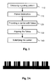
- method steps of recording machine-readable information on an article include a grating pattern step 110 of selecting a wavelength or wavelength range for reading the information, and selecting or designing a beam-splitting grating diffractive pattern, also referred to as a diffractive pattern generator, for diffracting, or splitting, a beam of electro-magnetic (EM) radiation into a plurality of sub-beams, thus encoding the information readable from an image produced by the sub-beams on a screen or in a reading/decoding device.
- the grating pattern is designed for a predefined wavelength or wavelength range.
- beam-splitting gratings also referred to as supergratings or Dammann gratings, produce sub-beams of equal or close energy values, which is beneficial for machine-reading applications.
- the beam-splitting grating pattern on a flake provides at least 3 or more sub-beams differing in energy no more that 5 times when illuminated with a monochrome EM beam having a predetermined wavelength, which for visible light means providing at least 3 spots with brightness (luminance) values differing no more than 5 times.
- Methods of designing supergratings are disclosed, for example, in Diffractive Optics, O'Shea et all., SPIE Press, 2004, pp. 84-92 and 122-124 , and U.S.
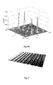
- Fig. 2A shows a grating profile of a first-order beam-splitting Dammann grating made by superposition of two regular gratings having different grating frequencies, designed for splitting an incident light beam into five sub-beams of equal intensity and several other sub-beams of lesser intensity.
- the supergratings are capable of generating a variety of patterns suitable for recognition and decoding, such as an array of spots, a grid, etc.
- the beam-splitting grating pattern is a cross-grating diffractive pattern providing a two-dimensional pattern of light spots.
- a cross-grating diffractive pattern is made of two regular, sinusoidal, mutually-orthogonal gratings having equal periods.
- the two gratings can be irregular and non-sinusoidal, such as rectangular, triangle, etc. or have different periods.
- An optional flake fabrication step 115 includes manufacturing of flakes having the predetermined beam splitting grating thereon.
- the flakes may be chosen from a pre-existing stock.
- the flakes include several thin film layers deposited in vacuum onto a polyester substrate and defoliated from the substrate and ground to desirable size, such as discloses in U.S. Patents Nos. 6,838,166 issued January 4, 2005, in the name of Phillips et al. , 6,818,299 issued November 16, 2004, in the name of Phillips et al. , 6,808,806 issued October 26, 2004, in the name of Phillips et al.
- the flakes are manufactured as taught in U.S. Application No. 20060228553 published October 12, 2006 by Argoitia et al ., incorporated herein by reference, that is one or more thin film layers are deposited onto a substrate embossed with the beam-splitting diffractive grating, and the coated substrate is cut to a predetermined size and shape.
- such flakes are fabricated by depositing a magnetic material 410 onto a thin polyester substrate 400 embossed with the beam-splitting diffractive grating, and then either a metallic reflector or a color-shifting optical stack 420.
- a layer of a hydrophobic or oleophobic material 430 is deposited as the last layer.
- the polyester substrate 400 with vacuum deposited layers 410 - 430 is cut into flakes having a size of 50 microns to 750 microns.
- a carrier 3 having flakes 2 dispersed therein is provided onto the surface of the article 1.
- the carrier 3 and the flakes 2 form an ink, which is printed onto the article 1.
- the flakes 2 have the beam-splitting grating pattern thereon.
- the flakes 2 are aligned parallel to each other and to an imaginable sloped plane forming a slope angle 16 with the surface of the article 1.
- the flakes include a magnetically responsive material and are aligned using a magnetic field having magnetic field lines oriented at the slope angle 16 to the surface of the article 1.
- the flakes are oriented using an electrostatic field. The alignment of the flakes will be discussed in more detail further with reference to an irradiation step 160 shown in Fig. 4 .
- the carrier 3 with the flakes 2 is solidified, for example by curing using any known conventional method, for example, UV or e-beam irradiation, solvent evaporation, etc.
- the steps 110 - 140 provide the article 1 with the information encoded on the flakes in the beam-splitting grating pattern.
- a method of obtaining the information from the article 1 shown in Fig. 3 includes the following steps: an article step 150, the irradiation step 160, and an information step 170.
- the article 1 having the information recorded using a beam-splitting grating pattern as described above is provided. It includes the flakes 2 having the beam-splitting grating pattern thereon; all of the flakes 2 are aligned parallel to the sloped plane forming the slope angle 16 with the surface of the article 1.
- the article 1 is irradiated with a beam of electro-magnetic (EM) radiation from a radiation source 5 shown in Fig. 3 .
- the radiation provided by the radiation source 5 is within the range of electromagnetic spectrum detectable by an optical decoding device.
- the radiation source 5 can be a monochromatic source or a polychromatic source, it can provide visible light or invisible radiation.
- the radiation source 5 is a 650-nm laser.
- the wavelength or wavelength range of the beam provided by the radiation source 5 is the same as one chosen in the grating pattern step 110 shown in Fig. 1 .
- the beam 4 from the radiation source 5 impinges on the printed article 1 and is reflected to a screen 6.
- the screen 6 can replaced with a detector of a reading/decoding device.
- the process of "reflection” is understood here as including both specular reflection and diffraction.
- a portion of the beam is reflected from the beam-splitting grating pattern on the flakes 2, forming an arrangement of sub-beams and an array of spots 8-12 on the screen 6.
- Another portion of the beam is reflected from the surface of the article 1; either by the surface of the carrier 3, or by a protective or other optional layer coated on top of the carrier 3.
- the surface reflection may present the problem illustrated by Fig. 5 , wherein the flakes 92 having the same grating pattern as flakes 2 shown in Fig. 3 , are aligned parallel to the surface of the article 91. A portion of the beam 4 is reflected from the surface of the article 91 forming a surface reflection sub-beam 13 and a surface reflection spot 14 on the screen 6.
- the surface reflection spot 14 distorts the image formed by the arrangement of sub-beams and may cause errors in reading the information.
- the flakes 2 are aligned parallel to the sloped plane forming the slope angle 16 with the surface of the article 1, as shown in Fig. 3 .
- the aligning step is such, that when_the article 1 is irradiated with the EM beam 4, the slope angle 16 provides a spatial separation between the arrangement of sub-beams and the surface reflection sub-beam 13, which appears on the screen 6 as a separation 15 between the surface reflection spot 14 and the array of spots 8-12 provided by the arrangement of sub-beams, thus enabling machine-reading of the reflected image.
- the slope angle 16 is greater than 5 degrees and less than 45 degrees to provide enough separation from the surface reflected spot 14 to the array of spots 8 - 12 in order to avoid superposition of images.
- the flakes are aligned so that grating vectors of all the flakes, that is vectors lying in the plane of the flakes and orthogonal to the grating grooves, are parallel to each other and form the slope angle with the surface of the article.
- the grating grooves of all the flakes are aligned at the slope angle to the surface of the article, and grooves of one flake are parallel to grooves of another flake.
- Such alignment of the grooves provides that the same position of the article 1 in respect to the radiation source 5 and the screen 6 is the best both for maximizing the separation 15 between the surface reflection spot 14 and the array of spots 8 - 12, and for maximizing the power of diffracted sub-beams.
- the direction of the grooves is not the same as the direction of the flakes slope in respect to the surface.
- such coating can be made using a magnetic field to align the flakes horizontally with all the grooves in the same direction, solidifying the coating, and then adding another uneven coating having a wedge profile.
- the information is obtained from the arrangement of sub-beams.
- the pattern of the sub-beams and light spots on the screen is predetermined by the beam-splitting grating design.
- the spots 8-12 produced on the screen 6 by the arrangement of sub-beams relate the information by the presence or absence of the array of the spots 8 - 12, the mutual layout and brightness of the spots, etc.
- more complicated images formed as discussed below contain more information than an array of light spots.
- the information may be obtained by a human observer, or by optical sensors thus enabling machine reading of the information.
- the obtained information is compared with information stored in the reader to verify the authenticity of the obtained information and the article.
- Figs. 6A and 6B two beam-splitting grating patterns are shown in Figs. 6A and 6B , where white regions correspond to debossed areas of the grating, and black regions - to embossed areas, also referred to as grooves.
- the grating of Fig. 6A has a one-dimensional Dammann grating pattern, and the grating shown in Fig. 6B - a two dimensional Dammann grating pattern.
- 4 pixels In X-direction, 4 pixels have a state 0, or "debossed", followed by four pixels having a state 1, or "embossed”. This pattern repeats in X direction, that is row wise in respect to Fig.
- the gratings shown in Figs. 6A and 6B are designed for splitting a laser beam into an arrangement of sub-beams of approximately equal intensity, providing a pattern of bright spots on a screen.
- the grating shown in Fig. 6B provides a square pattern of spots.
- the depth of embossing is chosen of about 325nm to provide the maximum efficiency for the predefined wavelength of the laser beam having a wavelength of 633 - 650nm.
- the Damman grating pattern has black and white pixels providing 0 and ⁇ relative phase values. This phase profile is embossed in aluminum coated polyester in a manner that the round trip optical path length difference between the black and white pixels is ⁇ at the required angle of incidence and center wavelength of illumination.
- both ⁇ 1 diffraction orders appear symmetrically deviated from the specular reflection direction in two orthogonal axes.
- the Y-direction spatial frequency encoding is three times that of the X-direction spatial frequency encoding. Consequently, the ⁇ 1 orders diffracted along the Y-direction appears three times as dispersed as the X-direction diffracted spots.
- the X- and Y-direction first order steering angle is approximately 1/8 and 3/8 of ratio of wavelength and encoding pixel size.
- the diffraction efficiency for each of the four first order spots is approximately 20% as illustrated by Fig. 6C , if there are no other undesirable defects such as non ⁇ phase step and non equal width of black and white pixels.
- a single flake having a beam-splitting grating pattern is shown in Fig. 7 .
- the flake is made of at least one layer of a magnetic material about 100nm thick.
- the flake has a multi-layered structure such as disclosed in the aforementioned U.S. Patents Nos. 6,838,166 , 6,818,299 , 6,808,806 , 7,241,489 and the U.S. Patent Application No. 20060228553 .
- one side of the flake shown in Fig. 7 is coated with a hydrophobic or oleophobic material, or another carrier- repellent material depending on the material of the ink carrier, for facilitating alignment of the flakes this side up, as disclosed in a co-pending U.S. Patent Application Ser. No. 12/051,164 filed March 19, 2008 and co-authored by a co-inventor of the instant invention.
- the carrier-repellent material is a hydrophobic material for flakes used in a water-based carrier, or an oleophobic material for flakes in an oil-based carrier or in another organic carrier.
- the choice of the carrier-repellent material depends on the type of the carrier, so that a carrier-repellent surface is not-wettable by the carrier, that is a contact angle between the surface and the liquid carrier is greater than 90°.
- the hydrophobic material is scandium fluoride or WR1 Patinal® manufactured by Merck.
- the grated diffractive flakes such as one shown in Fig. 7 , have an average size in the range of 5x5microns to 500x500microns, and an average thickness is in the range of 0.05 to 10 microns.
- a diameter of a laser beam is about 2 mm, therefore multiple flakes are irradiated simultaneously by the same laser beam.
- Each grated flake having a beam-splitting grating thereon provides a beam-splitting effect for a portion of the beam impinging on the surface of this flake.
- the reflected light spots on a screen or detector, such as shown in Fig. 3 is a cumulative result of reflecting different portions of the beam from different flakes.
- all grated flakes within a beam-spot-size region on an article have the same grating pattern, for example such as one shown in Fig. 7 , for providing a strong, well-readable image, visible or invisible, on a detector.
- a grating pattern for example such as one shown in Fig. 7
- other types of flakes can be present in the carrier, for example thin-film color-shifting flakes.
- Fig. 1 An alternative embodiment of the instant invention will be described now with reference to Fig. 1 .
- Two or more different beam-splitting patterns are chosen in the grating pattern step 110, and two or more types of grated flakes, having the chosen beam-splitting patterns thereon, are provided to the surface of an article within a carrier in the coating step 120.
- the flake alignment step 130 all the flakes aligned at the same slope angle. Accordingly, when the article is irradiated with a beam of light, or invisible EM radiation, the beam is split into an arrangement of sub-beams which is combination of sub-beam arrangements provided by each of the chosen grating patterns.
- the laser beam impinging on the article in a region 300 is reflected by first flakes 310 and second flakes 320 having different beam-splitting grating patterns thereon.
- the first flakes 310 provide a first array of light spots 340 on a screen 330
- the second flakes 320 provide a second array of light spots 350.
- FIG. 9 displaying a cross-section of an article.
- a substrate 500 is coated with a first ink layer 510 containing first flakes 515 having a beam-splitting grating pattern thereon.
- the carrier of the first ink layer 510 is solidified.
- a second ink layer 520 contains second flakes 525 is printed on the first ink layer 510.
- the second flakes 525 have a beam-splitting grating pattern thereon, the same or different from the beam-splitting grating pattern of the first flakes 515.
- the second flakes 515 are aligned in a second direction 526, forming a second slope angle with the surface of the article, different from the first slope angle of the first direction 516. After that, the carrier of the second ink layer is also solidified. If a two-layered structure made as described above is irradiated with a beam of light, a screen 530 has two arrays of light spots 540 and 550. The two arrays are spatially separated from each other due to the difference between the first and second slope angles, and each of them is spatially separated from the surface reflection spot 14.
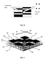
- a beam-splitting grating pattern forming a rectangular pattern of four light spots is shown schematically in Fig 10 . It has the same parameters of the grating as the pattern shown in Fig. 6 .
- elaborated images can be produced by light reflected from printed articles formed using diluted inks in the two-step printing method.
- flakes are aligned in one direction for forming a first line of dots on a screen.
- a second layer, printed over the first layer contains flakes aligned normally to the flakes within the first layer to form a second line of dots perpendicular to the first line.
- the two-layered structure is shown schematically in Fig. 11 .
- a substrate 201 is coated with a first ink layer 202 of a carrier containing first magnetic flakes 203 having a beam-splitting grating pattern, magnetically oriented in a first direction 204.
- a second ink layer 205 of the same ink is printed over the first ink layer 202, it contains second flakes 206, similar to the first flakes 203, but magnetically oriented in a second direction 207, normal to the first direction 204.
- the article When irradiated with a laser beam, the article provides an arrangement of dots in the pattern of a grid.
- the beam-splitting grating pattern of the first flakes 203 is different from the beam-splitting grating pattern of the second flakes 206.
- the aforedescribed article can be used for forming an image on a screen by reflecting a beam of EM radiation towards the screen.
- the information on the article can be detected by a reader having an illumination subsystem to direct a beam of EM radiation on the article, and an image detecting subsystem receiving and processing the radiation reflected from the article.
- the illumination subsystem includes a commercially available laser
- the image detecting subsystem includes an array of charge-coupled devices (CCD array).
Landscapes
- Chemical & Material Sciences (AREA)
- Engineering & Computer Science (AREA)
- Physics & Mathematics (AREA)
- General Physics & Mathematics (AREA)
- Organic Chemistry (AREA)
- Nanotechnology (AREA)
- Condensed Matter Physics & Semiconductors (AREA)
- Composite Materials (AREA)
- Health & Medical Sciences (AREA)
- Materials Engineering (AREA)
- Crystallography & Structural Chemistry (AREA)
- Toxicology (AREA)
- Computer Security & Cryptography (AREA)
- General Health & Medical Sciences (AREA)
- Spectroscopy & Molecular Physics (AREA)
- Credit Cards Or The Like (AREA)
- Diffracting Gratings Or Hologram Optical Elements (AREA)
- Optical Recording Or Reproduction (AREA)
- Photometry And Measurement Of Optical Pulse Characteristics (AREA)
Applications Claiming Priority (1)
| Application Number | Priority Date | Filing Date | Title |
|---|---|---|---|
| US91342307P | 2007-04-23 | 2007-04-23 |
Publications (2)
| Publication Number | Publication Date |
|---|---|
| EP1986138A2 true EP1986138A2 (de) | 2008-10-29 |
| EP1986138A3 EP1986138A3 (de) | 2009-08-12 |
Family
ID=39493913
Family Applications (1)
| Application Number | Title | Priority Date | Filing Date |
|---|---|---|---|
| EP08007872A Withdrawn EP1986138A3 (de) | 2007-04-23 | 2008-04-23 | Verfahren zur Aufzeichnung maschinenlesbarer Informationen |
Country Status (8)
| Country | Link |
|---|---|
| US (1) | US20080290179A1 (de) |
| EP (1) | EP1986138A3 (de) |
| JP (1) | JP2008287712A (de) |
| KR (1) | KR20080095203A (de) |
| CN (1) | CN101293443A (de) |
| AU (1) | AU2008201769A1 (de) |
| CA (1) | CA2629159A1 (de) |
| TW (1) | TW200912765A (de) |
Families Citing this family (3)
| Publication number | Priority date | Publication date | Assignee | Title |
|---|---|---|---|---|
| AU2008219354B2 (en) | 2007-09-19 | 2014-02-13 | Viavi Solutions Inc. | Anisotropic magnetic flakes |
| CN110751255B (zh) * | 2019-09-18 | 2023-09-19 | 上海鹄恩信息科技有限公司 | 光栅存储结构、基于光栅存储结构的信息解码方法及装置 |
| CN113031141A (zh) * | 2021-04-02 | 2021-06-25 | 中国科学院光电技术研究所 | 一种基于重力场加工闪耀光栅的方法 |
Citations (10)
| Publication number | Priority date | Publication date | Assignee | Title |
|---|---|---|---|---|
| US5101184A (en) | 1988-09-30 | 1992-03-31 | Lgz Landis & Gyr Zug Ag | Diffraction element and optical machine-reading device |
| US5116408A (en) | 1989-03-27 | 1992-05-26 | Crozer Veva W | Water-based wood stain |
| US6415081B1 (en) | 1999-08-05 | 2002-07-02 | Daniel Levner | Synthesis of supergratings by fourier methods |
| US6808806B2 (en) | 2001-05-07 | 2004-10-26 | Flex Products, Inc. | Methods for producing imaged coated articles by using magnetic pigments |
| US6818299B2 (en) | 2001-04-27 | 2004-11-16 | Flex Products, Inc. | Multi-layered magnetic pigments and foils |
| US6841238B2 (en) | 2002-04-05 | 2005-01-11 | Flex Products, Inc. | Chromatic diffractive pigments and foils |
| US6902807B1 (en) | 2002-09-13 | 2005-06-07 | Flex Products, Inc. | Alignable diffractive pigment flakes |
| US6975765B2 (en) | 2003-05-06 | 2005-12-13 | New Light Industries, Ltd. | Optically variable form birefringent structure and method and system and method for reading same |
| US20060228553A1 (en) | 2002-09-13 | 2006-10-12 | Jds Uniphase Corporation | High chroma optically variable color-shifting glitter |
| US7241489B2 (en) | 2002-09-13 | 2007-07-10 | Jds Uniphase Corporation | Opaque flake for covert security applications |
Family Cites Families (10)
| Publication number | Priority date | Publication date | Assignee | Title |
|---|---|---|---|---|
| GB9019784D0 (en) * | 1990-09-10 | 1990-10-24 | Amblehurst Ltd | Security device |
| CA2110681A1 (en) * | 1991-06-05 | 1992-12-10 | Peter Samuel Atherton | Optical memories incorporating diffraction gratings |
| EP0556449B1 (de) * | 1992-02-21 | 1997-03-26 | Hashimoto Forming Industry Co., Ltd. | Lackierung mit magnetisch hergestelltem Muster und lackiertes Produkt mit magnetisch hergestelltem Muster |
| US6088161A (en) * | 1993-08-06 | 2000-07-11 | The Commonwealth Of Australia Commonwealth Scientific And Industrial Research Organization | Diffractive device having a surface relief structure which generates two or more diffraction images and includes a series of tracks |
| US6476943B1 (en) * | 1999-02-23 | 2002-11-05 | Virtual Pro, Inc. | Distance measurement apparatus |
| DE19907697A1 (de) * | 1999-02-23 | 2000-08-24 | Giesecke & Devrient Gmbh | Wertdokument |
| TW452740B (en) * | 1999-08-09 | 2001-09-01 | Ind Tech Res Inst | Diffraction type anti-counterfeiting tag for both of bare eye reading and machine reading |
| GB0016359D0 (en) * | 2000-07-03 | 2000-08-23 | Optaglio Ltd | Optical apparatus |
| WO2002069307A2 (en) * | 2001-02-23 | 2002-09-06 | Technical Graphics Security Products, Llc | Security label having security element and method of making same |
| AU2008201211B2 (en) * | 2007-03-21 | 2013-09-26 | Viavi Solutions Inc. | A surface treated flake |
-
2008
- 2008-04-17 CA CA002629159A patent/CA2629159A1/en not_active Abandoned
- 2008-04-22 AU AU2008201769A patent/AU2008201769A1/en not_active Abandoned
- 2008-04-22 US US12/107,152 patent/US20080290179A1/en not_active Abandoned
- 2008-04-22 JP JP2008111712A patent/JP2008287712A/ja not_active Withdrawn
- 2008-04-22 KR KR1020080037302A patent/KR20080095203A/ko not_active Withdrawn
- 2008-04-22 TW TW097114668A patent/TW200912765A/zh unknown
- 2008-04-23 CN CNA2008100939438A patent/CN101293443A/zh active Pending
- 2008-04-23 EP EP08007872A patent/EP1986138A3/de not_active Withdrawn
Patent Citations (11)
| Publication number | Priority date | Publication date | Assignee | Title |
|---|---|---|---|---|
| US5101184A (en) | 1988-09-30 | 1992-03-31 | Lgz Landis & Gyr Zug Ag | Diffraction element and optical machine-reading device |
| US5116408A (en) | 1989-03-27 | 1992-05-26 | Crozer Veva W | Water-based wood stain |
| US6415081B1 (en) | 1999-08-05 | 2002-07-02 | Daniel Levner | Synthesis of supergratings by fourier methods |
| US6818299B2 (en) | 2001-04-27 | 2004-11-16 | Flex Products, Inc. | Multi-layered magnetic pigments and foils |
| US6838166B2 (en) | 2001-04-27 | 2005-01-04 | Flex Products, Inc. | Multi-layered magnetic pigments and foils |
| US6808806B2 (en) | 2001-05-07 | 2004-10-26 | Flex Products, Inc. | Methods for producing imaged coated articles by using magnetic pigments |
| US6841238B2 (en) | 2002-04-05 | 2005-01-11 | Flex Products, Inc. | Chromatic diffractive pigments and foils |
| US6902807B1 (en) | 2002-09-13 | 2005-06-07 | Flex Products, Inc. | Alignable diffractive pigment flakes |
| US20060228553A1 (en) | 2002-09-13 | 2006-10-12 | Jds Uniphase Corporation | High chroma optically variable color-shifting glitter |
| US7241489B2 (en) | 2002-09-13 | 2007-07-10 | Jds Uniphase Corporation | Opaque flake for covert security applications |
| US6975765B2 (en) | 2003-05-06 | 2005-12-13 | New Light Industries, Ltd. | Optically variable form birefringent structure and method and system and method for reading same |
Non-Patent Citations (1)
| Title |
|---|
| O'SHEA: "Diffractive Optics", 2004, SPIE PRESS, pages: 84 - 92 |
Also Published As
| Publication number | Publication date |
|---|---|
| CN101293443A (zh) | 2008-10-29 |
| EP1986138A3 (de) | 2009-08-12 |
| US20080290179A1 (en) | 2008-11-27 |
| CA2629159A1 (en) | 2008-10-23 |
| JP2008287712A (ja) | 2008-11-27 |
| KR20080095203A (ko) | 2008-10-28 |
| AU2008201769A1 (en) | 2008-11-06 |
| TW200912765A (en) | 2009-03-16 |
Similar Documents
| Publication | Publication Date | Title |
|---|---|---|
| KR102670356B1 (ko) | 배향된 비-구형 편원 자성 또는 자화성 안료 입자를 포함하는 광학 효과층을 생성하기 위한 어셈블리 및 공정 | |
| KR102670760B1 (ko) | 배향된 비-구형 편원 자성 또는 자화성 안료 입자를 포함하는 광학 효과층을 생성하기 위한 어셈블리 및 공정 | |
| CN101011916B (zh) | 具有增强防伪特性的图案光学结构 | |
| JP4961944B2 (ja) | 表示体及び印刷物 | |
| KR102670810B1 (ko) | 배향된 비-구형 편원 자성 또는 자화성 안료 입자를 포함하는 광학 효과층을 생성하기 위한 어셈블리 및 공정 | |
| US20210268825A1 (en) | Optically variable security element having reflective surface region | |
| CN101666886B (zh) | 显示旋转色移的光学装置 | |
| EP2056238B1 (de) | Informationsaufzeichnungsmedium sowie verfahren zur ablesung von informationen aus dem informationsaufzeichnungsmedium | |
| RU2370376C2 (ru) | Решетчатое изображение с одним или несколькими решетчатыми полями | |
| JP6707926B2 (ja) | 識別システム、識別方法及びプログラム | |
| US20160339733A1 (en) | Security elements and methods of their manufacture | |
| CN1265214A (zh) | 衍射表面图形 | |
| WO2017137720A1 (en) | Improvements in security devices | |
| WO2012015330A1 (ru) | Многослойный защитный элемент с переменным оптическим эффектом и защищенный от подделки документ | |
| EP3648982A1 (de) | Optische vorrichtungen und verfahren zu ihrer herstellung | |
| EP3114279B1 (de) | Verfahren zur herstellung eines sicherheitsdokuments | |
| EP1986138A2 (de) | Verfahren zur Aufzeichnung maschinenlesbarer Informationen | |
| RU2386544C1 (ru) | Защитный элемент на основе прозрачной полимерной пленки, способ его изготовления и полиграфическая продукция с такими элементами | |
| EP3210794B1 (de) | Mehrschichtiger polymerartikel, wie etwa ein identifikationsdokument | |
| EP4067105A1 (de) | Fälschungssicheres optisches element und fälschungssicheres optisches produkt | |
| US12293252B2 (en) | Encoding element and anti-counterfeiting product | |
| CN112823315B (zh) | 一体化3维显示体以及识别信息记录方法 |
Legal Events
| Date | Code | Title | Description |
|---|---|---|---|
| PUAI | Public reference made under article 153(3) epc to a published international application that has entered the european phase |
Free format text: ORIGINAL CODE: 0009012 |
|
| AK | Designated contracting states |
Kind code of ref document: A2 Designated state(s): AT BE BG CH CY CZ DE DK EE ES FI FR GB GR HR HU IE IS IT LI LT LU LV MC MT NL NO PL PT RO SE SI SK TR |
|
| AX | Request for extension of the european patent |
Extension state: AL BA MK RS |
|
| PUAL | Search report despatched |
Free format text: ORIGINAL CODE: 0009013 |
|
| AK | Designated contracting states |
Kind code of ref document: A3 Designated state(s): AT BE BG CH CY CZ DE DK EE ES FI FR GB GR HR HU IE IS IT LI LT LU LV MC MT NL NO PL PT RO SE SI SK TR |
|
| AX | Request for extension of the european patent |
Extension state: AL BA MK RS |
|
| RIC1 | Information provided on ipc code assigned before grant |
Ipc: G03H 1/00 20060101ALI20090703BHEP Ipc: B29C 59/00 20060101ALI20090703BHEP Ipc: G07D 7/12 20060101ALI20090703BHEP Ipc: G02B 6/34 20060101ALI20090703BHEP Ipc: C09C 1/00 20060101ALI20090703BHEP Ipc: B42D 15/00 20060101ALI20090703BHEP Ipc: B41M 3/14 20060101ALI20090703BHEP Ipc: G06K 19/00 20060101ALI20090703BHEP Ipc: G06K 19/16 20060101AFI20080617BHEP |
|
| AKX | Designation fees paid | ||
| STAA | Information on the status of an ep patent application or granted ep patent |
Free format text: STATUS: THE APPLICATION IS DEEMED TO BE WITHDRAWN |
|
| 18D | Application deemed to be withdrawn |
Effective date: 20100413 |
|
| REG | Reference to a national code |
Ref country code: DE Ref legal event code: 8566 |