EP1986137A2 - Method and device for checking the integrity of a logical signal, in particular a clock signal - Google Patents
Method and device for checking the integrity of a logical signal, in particular a clock signal Download PDFInfo
- Publication number
- EP1986137A2 EP1986137A2 EP08000427A EP08000427A EP1986137A2 EP 1986137 A2 EP1986137 A2 EP 1986137A2 EP 08000427 A EP08000427 A EP 08000427A EP 08000427 A EP08000427 A EP 08000427A EP 1986137 A2 EP1986137 A2 EP 1986137A2
- Authority
- EP
- European Patent Office
- Prior art keywords
- flip
- flop
- signal
- delay
- synchronous
- Prior art date
- Legal status (The legal status is an assumption and is not a legal conclusion. Google has not performed a legal analysis and makes no representation as to the accuracy of the status listed.)
- Withdrawn
Links
- 238000000034 method Methods 0.000 title claims abstract description 22
- 230000001133 acceleration Effects 0.000 claims abstract description 27
- 230000001360 synchronised effect Effects 0.000 claims description 73
- 238000001514 detection method Methods 0.000 claims description 23
- 102100021867 Natural resistance-associated macrophage protein 2 Human genes 0.000 claims description 12
- 108091006618 SLC11A2 Proteins 0.000 claims description 12
- 238000005070 sampling Methods 0.000 claims description 11
- 102100024099 Disks large homolog 1 Human genes 0.000 claims description 7
- 101001053984 Homo sapiens Disks large homolog 1 Proteins 0.000 claims description 7
- 101000951365 Homo sapiens Disks large-associated protein 5 Proteins 0.000 claims description 7
- 101001122448 Rattus norvegicus Nociceptin receptor Proteins 0.000 claims description 5
- 238000013479 data entry Methods 0.000 claims description 2
- 230000000630 rising effect Effects 0.000 description 22
- 238000004416 surface enhanced Raman spectroscopy Methods 0.000 description 17
- 238000002347 injection Methods 0.000 description 13
- 239000007924 injection Substances 0.000 description 13
- 230000003071 parasitic effect Effects 0.000 description 12
- 238000010586 diagram Methods 0.000 description 8
- 238000012544 monitoring process Methods 0.000 description 7
- 230000000694 effects Effects 0.000 description 4
- 244000045947 parasite Species 0.000 description 4
- 102100024117 Disks large homolog 2 Human genes 0.000 description 3
- 101001053980 Homo sapiens Disks large homolog 2 Proteins 0.000 description 3
- 101000590691 Homo sapiens MAGUK p55 subfamily member 2 Proteins 0.000 description 3
- 238000004364 calculation method Methods 0.000 description 3
- 230000004044 response Effects 0.000 description 3
- 230000007704 transition Effects 0.000 description 3
- 239000000872 buffer Substances 0.000 description 2
- 230000000717 retained effect Effects 0.000 description 2
- 238000013459 approach Methods 0.000 description 1
- 230000005540 biological transmission Effects 0.000 description 1
- 230000006378 damage Effects 0.000 description 1
- 230000003111 delayed effect Effects 0.000 description 1
- 238000013461 design Methods 0.000 description 1
- 235000021183 entrée Nutrition 0.000 description 1
- 210000001061 forehead Anatomy 0.000 description 1
- 238000013178 mathematical model Methods 0.000 description 1
- 210000000056 organ Anatomy 0.000 description 1
- 230000000737 periodic effect Effects 0.000 description 1
- 230000002085 persistent effect Effects 0.000 description 1
- 239000004065 semiconductor Substances 0.000 description 1
- 230000035945 sensitivity Effects 0.000 description 1
- 239000000243 solution Substances 0.000 description 1
- 238000012546 transfer Methods 0.000 description 1
- 230000001052 transient effect Effects 0.000 description 1
- 230000001960 triggered effect Effects 0.000 description 1
Images


Classifications
-
- G—PHYSICS
- G06—COMPUTING; CALCULATING OR COUNTING
- G06K—GRAPHICAL DATA READING; PRESENTATION OF DATA; RECORD CARRIERS; HANDLING RECORD CARRIERS
- G06K19/00—Record carriers for use with machines and with at least a part designed to carry digital markings
- G06K19/06—Record carriers for use with machines and with at least a part designed to carry digital markings characterised by the kind of the digital marking, e.g. shape, nature, code
- G06K19/067—Record carriers with conductive marks, printed circuits or semiconductor circuit elements, e.g. credit or identity cards also with resonating or responding marks without active components
- G06K19/07—Record carriers with conductive marks, printed circuits or semiconductor circuit elements, e.g. credit or identity cards also with resonating or responding marks without active components with integrated circuit chips
- G06K19/073—Special arrangements for circuits, e.g. for protecting identification code in memory
- G06K19/07309—Means for preventing undesired reading or writing from or onto record carriers
- G06K19/07363—Means for preventing undesired reading or writing from or onto record carriers by preventing analysis of the circuit, e.g. dynamic or static power analysis or current analysis
Landscapes
- Engineering & Computer Science (AREA)
- Computer Hardware Design (AREA)
- Computer Security & Cryptography (AREA)
- General Engineering & Computer Science (AREA)
- Microelectronics & Electronic Packaging (AREA)
- Physics & Mathematics (AREA)
- General Physics & Mathematics (AREA)
- Theoretical Computer Science (AREA)
- Manipulation Of Pulses (AREA)
- Synchronisation In Digital Transmission Systems (AREA)
- Tests Of Electronic Circuits (AREA)
Abstract
Description
La présente invention concerne un procédé et un dispositif de vérification de l'intégrité d'un signal logique, notamment un signal d'horloge.The present invention relates to a method and a device for verifying the integrity of a logic signal, in particular a clock signal.
La présente invention concerne plus particulièrement un procédé et un dispositif de détection d'une accélération parasite d'un signal logique se traduisant par un rapprochement au-delà d'un seuil de rapprochement d'au moins deux fronts de variation d'un type déterminé du signal logique.The present invention more particularly relates to a method and a device for detecting a parasitic acceleration of a logic signal resulting in a reconciliation beyond a threshold of approximation of at least two variation fronts of a given type. of the logic signal.
Les circuits logiques présents dans les circuits intégrés sécurisés, comme les circuits intégrés pour cartes à puce, font l'objet de diverses attaques de la part de fraudeurs qui cherchent à découvrir leur structure et/ou les secrets qu'ils comprennent. Il s'agit par exemple de circuits de cryptographie de type DES, AES, RSA..., de microprocesseurs programmés pour exécuter des algorithmes de cryptographie, de banques de registres contenant des clefs secrètes, etc.The logic circuits present in secure integrated circuits, such as integrated circuits for smart cards, are the subject of various attacks by fraudsters who seek to discover their structure and / or secrets they understand. They are, for example, type DES, AES, RSA cryptography circuits, microprocessors programmed to execute cryptography algorithms, register banks containing secret keys, etc.
A l'heure actuelle, les méthodes de piratage les plus avancées consistent à injecter des erreurs dans un circuit intégré lors de l'exécution d'opérations dites sensibles, par exemple des opérations d'authentification ou des opérations d'exécution d'un algorithme de cryptographie.At the present time, the most advanced hacking methods consist in injecting errors into an integrated circuit during the execution of so-called sensitive operations, for example authentication operations or operations for executing an algorithm. cryptography.
De telles attaques, appelées attaques par injection d'erreur ou injection de faute, peuvent intervenir pendant des phases de calculs dits sensibles, par exemple pendant des phases de calcul d'un code d'identification ou pendant la lecture d'une clef de cryptographie dans une mémoire. Elles permettent, en combinaison avec des modèles mathématiques et à partir de résultats faux obtenus intentionnellement grâce à des perturbations, de définir un élément secret comme une clef de cryptage ou un mot de passe, de déduire la structure d'un algorithme de cryptographie et/ou les clefs secrètes que l'algorithme utilise, etc.Such attacks, called error injection or fault injection attacks, may occur during so-called sensitive calculation phases, for example during phases of calculating an identification code or during the reading of a cryptography key. in a memory. They allow, in combination with mathematical models and from false results obtained intentionally through disruption, to define a secret element as an encryption key or password, to derive the structure of a cryptographic algorithm and / or the secret keys that the algorithm uses, etc.
En particulier, les attaques localisées consistent à introduire des perturbations en un point déterminé du circuit, par exemple au moyen d'un faisceau laser ou un faisceau de rayon X. Une attaque localisée peut concerner la tension d'alimentation, un chemin de données, ou le signal d'horloge du circuit intégré.In particular, the localized attacks consist in introducing disturbances at a given point of the circuit, for example by means of a laser beam or an X-ray beam. A localized attack may concern the supply voltage, a data path, or the clock signal of the integrated circuit.
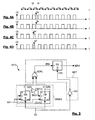
La présente invention concerne notamment la protection des circuits synchrones contre des attaques par injection d'erreur localisée dans le signal d'horloge. La
En raison de son effet sur les transitions de données dans les divers modules synchrones, le signal d'horloge CK est particulièrement vulnérable aux injections d'erreur. Cette vulnérabilité réside dans le fait qu'une attaque peut permettre de transférer une donnée dans des bascules dont l'entrée est connectée à un chemin de données à faible temps de propagation alors que des bascules dont l'entrée est connectée à un chemin de données ayant un temps de propagation plus long n'ont pas encore reçu la donnée.Because of its effect on data transitions in the various synchronous modules, the clock signal CK is particularly vulnerable to error injections. This vulnerability lies in the that an attack can transfer data into flip-flops whose input is connected to a low-delay data path while flip-flops whose input is connected to a data path with a delay longer have not received the data yet.
Ce problème est illustré sur la
Lorsqu'une donnée DT est appliquée à l'entrée de la bascule FF1, par exemple au cours d'un cycle T1 du signal d'horloge CK, la donnée est recopiée par la sortie de la bascule au cours d'un cycle T2 puis se propage jusqu'aux entrées des bascules FF2, FF3 pour être recopiée par les sorties des bascules FF2, FF3 au cours d'un cycle T3. La propagation de la donnée est illustrée par les
La donnée DT est fournie au point B par la bascule FF1 à un instant t2 correspondant au commencement du cycle T2. Elle se retrouve ainsi au point C à un instant t2'=t2+DLYa et au point D à un instant t2"=t2+DLYb. Les instants t2' et t2" doivent impérativement se trouver dans le cycle T2 à défaut de quoi la donnée ne serait pas recopiée par les bascules FF2 et FF3 au commencement du cycle T3.The data DT is supplied to the point B by the flip-flop FF1 at a time t2 corresponding to the beginning of the cycle T2. It is thus found at point C at a time t2 '= t2 + DLYa and at point D at a time t2 "= t2 + DLYb The instants t2' and t2" must imperatively be in the cycle T2, failing which the This data would not be copied by flip-flops FF2 and FF3 at the beginning of cycle T3.
A la lumière de cet exemple, il apparaît que le temps de propagation le plus long d'une donnée, à travers un chemin asynchrone reliant deux éléments synchrones, détermine la fréquence maximale du signal d'horloge, soit sa période T minimale, cette règle étant bien connue des concepteurs de circuits intégrés. Il apparaît également que si un fraudeur injecte un front d'horloge parasite dans le signal d'horloge à un instant situé entre l'instant t2' et t2", une erreur sur la donnée DT se produit dans le circuit synchrone car la bascule FF2 recopie la donnée tandis que la bascule FF3 ne la recopie pas, puisque la donnée n'est pas encore parvenue jusqu'à son entrée.In the light of this example, it appears that the longest propagation time of a data, through an asynchronous path connecting two synchronous elements, determines the maximum frequency of the clock signal, ie its minimum period T, this rule being well known to the designers of integrated circuits. It also appears that if a fraudster injects a parasitic clock edge into the clock signal at a time between time t2 'and t2 ", an error on data DT occurs in the synchronous circuit because the flip-flop FF2 copy the data while the flip flop FF3 does not copy it, since the data has not yet arrived until its entry.
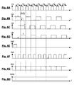
Les chronogrammes des
- injecter un créneau positif : sur la
figure 4A , un créneau parasite positif est injecté dans le signal d'horloge à l'instant te, - avancer un front : sur la
figure 4B , le front montant du créneau d'horloge du cycle T4 apparaît de façon anticipée à l'instant te au cours d'un cycle T3, - retarder un front : sur la
figure 4C , le front montant du créneau d'horloge CK du cycle T3 apparaît tardivement à un instant te' au cours du cycle T3, au lieu d'apparaître à un instant t3 situé au commencement de ce cycle, et - injecter un créneau négatif : sur la
figure 4A , un créneau parasite négatif est injecté dans un créneau d'horloge, ce qui provoque la division du créneau d'horloge en deux créneaux positifs distincts, le second apparaissant à un instant te" du cycle T3 et pouvant être considéré comme un créneau positif parasite.
- inject a positive niche: on the
Figure 4A a positive parasitic slot is injected into the clock signal at the instant te, - advance a front: on the
Figure 4B the rising edge of the clock pulse of cycle T4 appears early at time te during a cycle T3, - to delay a front: on the
figure 4C , the rising edge of the clock pulse CK of the cycle T3 appears late at a time te 'during the cycle T3, instead of appearing at a time t3 situated at the beginning of this cycle, and - inject a negative niche: on the
Figure 4A , a negative parasitic slot is injected into a clock slot, which causes the division of the clock slot into two distinct positive slots, the second appearing at a time t "of the T3 cycle and can be considered as a parasitic positive slot. .
De façon générale, ces diverses attaques visent à rapprocher deux fronts actifs du signal d'horloge afin de provoquer le déclenchement successif du circuit synchrone avec un intervalle de temps qui est inférieur au temps de propagation le plus long d'une donnée au sein du circuit. Chacun des cas représenté correspond ainsi à une accélération du signal d'horloge au delà d'un seuil de rapprochement des créneaux pouvant être toléré, et à une fréquence de fonctionnement supérieure à la fréquence de fonctionnement maximale du circuit synchrone.In general, these various attacks aim to bring two active edges closer to the clock signal in order to cause the synchronous circuit to be triggered successively with a time interval that is shorter than the longest propagation time of a datum within the circuit. . Each of the cases represented thus corresponds to an acceleration of the clock signal beyond a threshold of proximity of the slots that can be tolerated, and to an operating frequency higher than the maximum operating frequency of the synchronous circuit.
Pour contrer de telles attaques, les procédés habituellement mis en oeuvre consistent à détecter une anomalie dans les données fournies par les circuits synchrones concernés. Ces procédés reposent par exemple sur une redondance logicielle ou matérielle des circuits susceptibles d'attaque. La redondance logicielle consiste dans le fait de recalculer au moyen d'un programme le résultat fournit par un circuit synchrone, le calcul redondant étant effectué par un microprocesseur. Par ailleurs, la redondance matérielle consiste à reproduire en plusieurs exemplaires les parties "sensibles" d'un circuit synchrone, et de comparer les résultats fournis par les circuits redondants, le résultat majoritaire pouvant être retenu comme résultat fiable en cas de divergence de résultats. De façon générale, ces procédés entrainent une occupation importante de la surface de semi-conducteur disponible (redondance matérielle) ou un ralentissement notable du fonctionnement des circuits synchrones (redondance logicielle).To counter such attacks, the methods usually employed consist in detecting an anomaly in the data provided by the synchronous circuits concerned. These methods are based for example on a software or hardware redundancy circuits likely to attack. Software redundancy consists in the recalculating by means of a program the result provided by a synchronous circuit, the redundant calculation being carried out by a microprocessor. In addition, the hardware redundancy consists in reproducing in several copies the "sensitive" parts of a synchronous circuit, and comparing the results provided by the redundant circuits, the majority result being able to be retained as a reliable result in case of divergence of results. In general, these methods cause a significant occupation of the available semiconductor surface (hardware redundancy) or a significant slowdown in the operation of the synchronous circuits (software redundancy).
La présente invention propose une solution tout à fait différente. Au lieu de détecter une erreur de donnée consécutive à une injection d'erreur, qui constitue l'effet second de l'injection d'erreur, l'invention propose de détecter l'effet premier de l'injection d'erreur, c'est-à-dire l'apparition d'une anomalie dans le signal d'horloge, soit la détection d'une accélération de celui-ci.The present invention provides a completely different solution. Instead of detecting a data error following an error injection, which constitutes the second effect of the error injection, the invention proposes to detect the first effect of the error injection, that is, the occurrence of an anomaly in the clock signal, ie the detection of an acceleration thereof.
Ainsi, l'invention prévoit un procédé de détection d'une accélération d'un signal logique se traduisant par un rapprochement, au-delà d'un seuil de rapprochement, d'au moins deux fronts de variation d'un type déterminé du signal logique, comprenant les étapes consistant à prévoir au moins un premier bit de contrôle et un second bit de contrôle et conférer une valeur initiale au premier bit de contrôle et une valeur initiale au second bit de contrôle, à chaque front du type déterminé du signal logique, inverser la valeur du premier bit de contrôle après un premier délai et inverser la valeur du second bit de contrôle après un second délai inférieur au premier, et détecter une accélération quand les bits de contrôle ne présentent pas en même temps leurs valeurs initiales respectives ou leurs valeurs initiales respectives inversées.Thus, the invention provides a method of detecting an acceleration of a logic signal resulting in a reconciliation, beyond a threshold of approximation, of at least two variation fronts of a given type of the signal. logic, comprising the steps of providing at least a first control bit and a second control bit and providing an initial value to the first control bit and an initial value to the second control bit, each edge of the determined type of the logic signal. inverting the value of the first control bit after a first delay and inverting the value of the second control bit after a second delay less than the first, and detecting an acceleration when the control bits do not present their respective initial values at the same time or their respective initial values reversed.
Selon un mode de réalisation, le procédé comprend les étapes consistant à produire un signal d'erreur asynchrone ayant une valeur inactive et une valeur active, et porter le signal d'erreur asynchrone à la valeur active quand les deux bits de contrôle ne présentent pas en même temps leurs valeurs initiales respectives ou leurs valeurs initiales respectives inversées, et échantillonner le signal d'erreur asynchrone après chaque front de variation du type déterminé du signal logique, afin de filtrer des erreurs de synchronisation tolérées des deux bits de contrôle et de produire un signal d'erreur synchrone.According to one embodiment, the method comprises the steps of producing an asynchronous error signal having an inactive value and an active value, and bringing the asynchronous error signal to the active value when the two control bits do not present. at the same time their respective initial values or respective initial values inverted, and to sample the error signal asynchronously after each variation edge of the determined type of the logic signal, in order to filter tolerated synchronization errors of the two control bits and to produce a synchronous error signal.
Selon un mode de réalisation, le procédé comprend une étape consistant à rafraîchir cycliquement le signal d'erreur synchrone en synchronisation avec des fronts de variation du signal logique d'un type inverse au type déterminé, descendants ou montants.According to one embodiment, the method comprises a step of cyclically refreshing the synchronous error signal in synchronization with edges of variation of the logical signal of a type inverse to the determined type, descendants or amounts.
Selon un mode de réalisation, le procédé comprend les étapes consistant à prévoir au moins une première bascule synchrone cadencée par le signal logique et une seconde bascule synchrone cadencée par le signal logique, charger la valeur initiale du premier bit de contrôle dans la première bascule et la valeur initiale du second bit de contrôle dans la seconde bascule, et configurer les bascules pour qu'à chaque front du type déterminé du signal logique, la valeur du premier bit de contrôle s'inverse après le premier délai et la valeur du second bit de contrôle s'inverse après le second délai.According to one embodiment, the method comprises the steps of providing at least a first synchronous flip-flop clocked by the logic signal and a second synchronous flip-flop clocked by the logic signal, loading the initial value of the first control bit in the first flip-flop and the initial value of the second control bit in the second flip-flop, and configuring the flip-flops so that at each edge of the determined type of the logic signal, the value of the first control bit is reversed after the first delay and the value of the second bit control is reversed after the second delay.
Selon un mode de réalisation, l'étape de configuration des bascules comprend les étapes consistant à relier une sortie de données de la première bascule à une entrée de données de la seconde bascule par l'intermédiaire d'un circuit à retard introduisant le premier délai, et relier ou connecter une sortie de données de la seconde bascule à une entrée de données de la première bascule.According to one embodiment, the step of configuring the flip-flops comprises the steps of connecting a data output of the first flip-flop to a data input of the second flip-flop via a delay circuit introducing the first delay. , and connect or connect a data output of the second flip-flop to a data input of the first flip-flop.
Selon un mode de réalisation, l'étape de configuration des bascules comprend les étapes consistant à relier une sortie de données de la première bascule à une entrée de données de la première bascule par l'intermédiaire d'un circuit à retard introduisant le premier délai, et relier ou connecter une sortie de données de la seconde bascule à une entrée de données de la seconde bascule.According to one embodiment, the step of configuring the flip-flops comprises the steps of connecting a data output of the first flip-flop to a data input of the first flip-flop via a delay circuit introducing the first delay. , and connect or connect an output of data from the second flip-flop to a data input of the second flip-flop.
Selon un mode de réalisation, l'étape de chargement des bits de contrôle comprend une étape consistant à initialiser chaque bascule avec un signal de mise à 0 ou de mise à 1 de la bascule.According to one embodiment, the step of loading the control bits comprises a step of initializing each flip-flop with a setting signal of 0 or setting of the flip-flop.
Selon un mode de réalisation, le signal logique est un signal d'horloge.According to one embodiment, the logic signal is a clock signal.
Selon un mode de réalisation, le premier délai est au moins égal à un retard maximal de propagation asynchrone d'une donnée entre deux éléments synchrones cadencés par le signal d'horloge.According to one embodiment, the first delay is at least equal to a maximum delay of asynchronous propagation of data between two synchronous elements clocked by the clock signal.
Selon un mode de réalisation, le second délai est nul.According to one embodiment, the second delay is zero.
L'invention concerne également un dispositif de détection d'une accélération d'un signal logique, comprenant au moins une première bascule synchrone cadencée par le signal logique, recevant un premier bit de contrôle, et une seconde bascule synchrone cadencée par le signal logique, recevant un second bit de contrôle, les bascules étant agencées de manière qu'à chaque front du type déterminé du signal logique, la valeur du premier bit de contrôle s'inverse après un premier délai et la valeur du second bit de contrôle s'inverse après un second délai, des moyens pour charger une valeur initiale du premier bit de contrôle dans la première bascule et une valeur initiale du second bit de contrôle dans la seconde bascule, et des moyens pour fournir un signal d'erreur représentatif d'une accélération quand les deux bits ne présentent pas en même temps leurs valeurs initiales respectives ou leurs valeurs initiales respectives inversées.The invention also relates to a device for detecting an acceleration of a logic signal, comprising at least a first synchronous flip-flop clocked by the logic signal, receiving a first control bit, and a second synchronous flip-flop clocked by the logic signal, receiving a second control bit, the flip-flops being arranged so that at each edge of the determined type of the logic signal, the value of the first control bit is reversed after a first delay and the value of the second control bit is reversed after a second delay, means for loading an initial value of the first control bit in the first flip-flop and an initial value of the second control bit in the second flip-flop, and means for providing an error signal representative of an acceleration when the two bits do not present at the same time their respective initial values or their respective initial inverted values.
Selon un mode de réalisation, les moyens pour détecter une accélération comprennent des moyens pour produire un signal d'erreur asynchrone ayant une valeur inactive et une valeur active, et porter le signal d'erreur asynchrone à la valeur active quand les deux bits de contrôle ne présentent pas en même temps leurs valeurs initiales respectives ou leurs valeurs initiales respectives inversées, et des moyens pour échantillonner le signal d'erreur asynchrone après chaque front de variation du type déterminé du signal logique, afin de filtrer des erreurs de synchronisation tolérées des deux bits de contrôle et de produire un signal d'erreur synchrone.According to one embodiment, the means for detecting an acceleration comprise means for producing an asynchronous error signal having an inactive value and an active value, and carrying the signal of asynchronous error to the active value when the two control bits do not present at the same time their respective initial values or their respective initial inverted values, and means for sampling the asynchronous error signal after each variation front of the determined type of the logic signal, in order to filter tolerated synchronization errors of the two control bits and to produce a synchronous error signal.
Selon un mode de réalisation, les moyens pour échantillonner le signal d'erreur asynchrone sont agencés pour rafraîchir cycliquement le signal d'erreur synchrone en synchronisation avec des fronts de variation du signal logique d'un type inverse au type déterminé, descendants ou montants.According to one embodiment, the means for sampling the asynchronous error signal are arranged to cyclically refresh the synchronous error signal in synchronization with edges of variation of the logical signal of a type inverse to the determined type, descendants or amounts.
Selon un mode de réalisation, une sortie de données de la première bascule est reliée à une entrée de données de la seconde bascule par l'intermédiaire d'un circuit à retard introduisant le premier délai, et une sortie de données de la seconde bascule est reliée à une entrée de données de la première bascule.According to one embodiment, a data output of the first flip-flop is connected to a data input of the second flip-flop via a delay circuit introducing the first delay, and a data output of the second flip-flop is connected to a data entry of the first flip-flop.
Selon un mode de réalisation, une sortie de données de la première bascule est reliée à une entrée de données de la première bascule par l'intermédiaire d'un circuit à retard introduisant le premier délai, et une sortie de données de la seconde bascule est reliée à une entrée de données de la seconde bascule.According to one embodiment, a data output of the first flip-flop is connected to a data input of the first flip-flop via a delay circuit introducing the first delay, and a data output of the second flip-flop is connected to a data input of the second flip-flop.
Selon un mode de réalisation, chaque bascule comprend une entrée de mise à 0 ou de mise à 1 recevant un signal de contrôle pour charger dans la bascule la valeur initiale du bit de contrôle.According to one embodiment, each flip-flop includes a setting
Selon un mode de réalisation, le dispositif comprend une entrée fournissant le signal logique à surveiller et connectée à un fil d'horloge d'un circuit synchrone.According to one embodiment, the device comprises an input supplying the logic signal to be monitored and connected to a clock wire of a synchronous circuit.
Selon un mode de réalisation, premier délai est au moins égal à un retard maximal de propagation asynchrone d'une donnée entre deux éléments synchrones du circuit synchrone.According to one embodiment, the first delay is at least equal to a maximum delay of asynchronous propagation of data between two synchronous elements of the synchronous circuit.
Selon un mode de réalisation, le second délai est nul.According to one embodiment, the second delay is zero.
L'invention concerne également un circuit synchrone comprenant des modules synchrones cadencés par un signal logique véhiculé par un arbre d'horloge, comprenant un dispositif de détection selon l'invention, pour détecter des accélérations dans le signal logique.The invention also relates to a synchronous circuit comprising synchronous modules clocked by a logic signal carried by a clock tree, comprising a detection device according to the invention for detecting accelerations in the logic signal.
L'invention concerne également un circuit intégré comprenant des organes synchrones cadencés par un signal logique véhiculé par un bus d'horloge, et un dispositif de détection selon l'invention, pour détecter des accélérations dans le signal logique.The invention also relates to an integrated circuit comprising synchronous members clocked by a logic signal carried by a clock bus, and a detection device according to the invention for detecting accelerations in the logic signal.
Ces objets, caractéristiques et avantages ainsi que d'autres de la présente invention seront exposés plus en détail dans la description suivante de divers modes de réalisation d'un dispositif de détection selon l'invention, faite à titre non limitatif en relation avec les figures jointes parmi lesquelles :
- la
figure 1 précédemment décrite représente schématiquement un circuit synchrone comprenant un arbre d'horloge, - la
figure 2 précédemment décrite représente un circuit synchrone comprenant des chemins de données asynchrones, - la
figure 3A précédemment décrite représente un signal d'horloge appliqué au circuit synchrone et lesfigures 3B à 3E sont des chronogrammes représentant la propagation d'une donnée dans le circuit synchrone, - les
figures 4A à 4D précédemment décrites sont des chronogrammes représentant quatre types d'injection d'erreur conduisant à une accélération du signal d'horloge, - la
figure 5 représente un premier mode de réalisation d'un dispositif de détection selon l'invention, recevant un signal logique à surveiller, - les
figures 6A à 6H sont des chronogrammes illustrant le fonctionnement normal du dispositif de détection en l'absence d'erreur dans le signal surveillé, - les
figures 7A à 7H ,8A à 8H ,9A à 9H ,10A à 10H sont des chronogrammes illustrant le fonctionnement du dispositif de détection en réponse à une injection d'une erreur d'un premier type, d'un second type, d'un troisième type et d'un quatrième type, respectivement, dans le signal surveillé, - la
figure 11 représente une variante du dispositif de détection de lafigure 5 , - la
figure 12 représente un second mode de réalisation du dispositif de détection selon l'invention, et - la
figure 13 représente l'architecture d'un circuit intégré comprenant un dispositif de détection selon l'invention.
- the
figure 1 previously described schematically represents a synchronous circuit comprising a clock tree, - the
figure 2 previously described represents a synchronous circuit comprising asynchronous data paths, - the
figure 3A previously described represents a clock signal applied to the synchronous circuit and theFigures 3B to 3E are timing diagrams representing the propagation of data in the synchronous circuit, - the
Figures 4A to 4D previously described are timing diagrams representing four types of error injection leading to an acceleration of the clock signal, - the
figure 5 represents a first embodiment of a detection device according to the invention, receiving a logic signal to monitor, - the
Figures 6A to 6H are timing diagrams illustrating the normal operation of the detection device in the absence of an error in the monitored signal, - the
Figures 7A to 7H ,8A to 8H ,9A to 9H ,10A to 10H are timing diagrams illustrating the operation of the detection device in response to an injection of an error of a first type, a second type, a third type and a fourth type, respectively, into the monitored signal, - the
figure 11 represents a variant of the detection device of thefigure 5 , - the
figure 12 represents a second embodiment of the detection device according to the invention, and - the
figure 13 represents the architecture of an integrated circuit comprising a detection device according to the invention.
Dans les exemples qui viennent d'être décrits et dans l'ensemble de la présente demande, il est considéré que les fronts de variation du signal d'horloge provoquant le déclenchement des éléments synchrones d'un circuit synchrone, ou front actifs, sont des fronts montants. Toutefois, une convention inverse peut être retenue. Dans ce cas, ce qui est indiqué dans la présente demande au sujet des fronts montants concerne les fronts descendants.In the examples which have just been described and throughout the present application, it is considered that the edges of variation of the clock signal causing the triggering of the synchronous elements of a synchronous circuit, or active edge, are rising fronts. However, an inverse convention can be retained. In this case, what is stated in this application for rising fronts is for falling fronts.
La
Le registre SREG1 comprend deux bascules FFA, FFB comprenant chacune une entrée de donnée D, une sortie de données Q, une sortie de données inverseuse /Q, une entrée d'horloge CK, une entrée SET de mise à 1 et une entrée RST de mise à 0. Les bascules FFA, FFB reçoivent le signal d'horloge CK sur leur entrée d'horloge. La sortie Q de la bascule FFA fournit un bit de contrôle QA et est reliée à l'entrée D de la bascule FFB par l'intermédiaire d'un circuit DLG1 introduisant entre la sortie Q et l'entrée D un retard DLY1 qui est de durée inférieure à la période T du signal d'horloge CK. La sortie Q de la bascule FFB fournit un bit de contrôle QB et est connectée à l'entrée D de la bascule FFA. Un signal INIT est appliqué à l'entrée SET de la bascule FFA et à l'entrée RST de la bascule FFB.The register SREG1 comprises two flip-flops FFA, FFB each comprising a data input D, a data output Q, an inverting data output / Q, a clock input CK, a set input SET and an input RST of The FFA, FFB flip-flops receive the clock signal CK on their clock input. The Q output of the flip-flop FFA provides a control bit QA and is connected to the input D of the flip-flop FFB via a circuit DLG1 introducing between the output Q and the input D a delay DLY1 which is duration less than the period T of the clock signal CK. The Q output of the flip-flop FFB provides a control bit QB and is connected to the input D of the FFA flip-flop. An INIT signal is applied to the SET input of the FFA flip-flop and to the RST input of the FFB flip-flop.
Le circuit de surveillance WCT comprend une porte XOR1 de type OU EXCLUSIF, une porte inverseuse IV1 et une bascule FFC. La porte XOR1 reçoit les bits de contrôle QA, QB et fournit un signal d'erreur asynchrone ERS dont la valeur active est ici 0. La porte inverseuse IV1 reçoit le signal d'horloge CK et fournit un signal d'échantillonnage CKS. Le signal CKS est appliqué à l'entrée d'horloge de la bascule FFC. Celle-ci reçoit le signal ERS sur son entrée D et le recopie sur la sortie à chaque front montant du signal CKS, pour fournir un signal d'erreur synchrone SERS dont la valeur active est également 0.The monitoring circuit WCT comprises an XOR1 gate of EXCLUSIVE OR type, an inverting gate IV1 and an FFC flip-flop. The gate XOR1 receives the control bits QA, QB and supplies an asynchronous error signal ERS whose active value is here 0. The inverting gate IV1 receives the clock signal CK and supplies a sampling signal CKS. The signal CKS is applied to the clock input of the FFC flip-flop. This receives the signal ERS on its input D and copies it on the output at each rising edge of the signal CKS, to provide a synchronous error signal SERS whose active value is also 0.
Le registre à décalage SREG1 présente des cycles de décalage T1, T2, T3, T4, T5,... de période égale à la période T du signal d'horloge CK. Lorsque le signal INIT est appliqué aux bascules, par exemple un front montant du signal INIT, un mot de contrôle comprenant des bits de contrôle QA, QB respectivement égaux à 1 et 0 est chargé dans le registre à décalage. Les bits QA, QB du mot de contrôle se propagent ensuite en boucle fermée dans le registre, de sorte que la valeur fournie par le registre est égale à 10, puis 01, puis de nouveau 10, etc. comme illustré par le tableau ci-après.
Lorsque le registre contient l'une des valeurs 10 ou 01, le signal d'erreur ERS à la sortie de la porte XOR1 est égal à 1. Si l'une des combinaisons des bits de contrôle devient égale à "00" ou "11", le signal ERS passe à 0. Si l'erreur est persistante et existe encore lorsque le signal CKS présente un front montant, le signal SERS passe également à 0 indiquant ainsi qu'une accélération est intervenue dans le signal d'horloge CK. Une telle erreur est représentative d'une injection d'erreur dans signal d'horloge.When the register contains one of the values 10 or 01, the error signal ERS at the output of the gate XOR1 is equal to 1. If one of the combinations of the control bits becomes equal to "00" or "11" the signal ERS goes to 0. If the error is persistent and still exists when the signal CKS has a rising edge, the signal SERS also goes to 0 indicating that an acceleration has occurred in the clock signal CK. Such an error is representative of an error injection in a clock signal.
Le fonctionnement du dispositif DCT1 pendant des cycles T1, T2, T3, T4... du signal d'horloge est illustré par des chronogrammes sur les
- les
figures 6A à 10A représentent le signal d'horloge CK, - les
figures 6B à 10B représentent le bit de contrôle QA, - les
figures 6C à 10C représentent un bit DB présent à l'entrée D de la bascule FFA, - les
figures 6D à 10D représentent le bit de contrôle QB, - les
figures 6E à 10E représentent le signal INIT, - les
figures 6F à 10F représentent le signal d'échantillonnage CKS, - les
figures 6G à 10G représentent le signal d'erreur asynchrone ERS, et - les
figures 6H à 10H représentent le signal d'erreur synchrone SERS.
- the
Figures 6A to 10A represent the clock signal CK, - the
Figures 6B to 10B represent the control bit QA, - the
FIGS. 6C to 10C represent a bit DB present at the input D of the FFA flip-flop, - the
Figures 6D to 10D represent the control bit QB, - the
Figures 6E to 10E represent the INIT signal, - the
Figures 6F to 10F represent the sampling signal CKS, - the
Figures 6G to 10G represent the ERS asynchronous error signal, and - the
Figures 6H to 10H represent the synchronous error signal SERS.
Les
Le signal d'erreur asynchrone ERS peut passer transitoirement à 0 (ou tendre vers 0) à chaque front montant du signal CK en raison des temps de commutation respectifs des bascules, qui peuvent être légèrement différents. Cette fluctuation de courte durée n'est pas reproduite par le signal SERS et est ainsi filtrée. En effet le signal d'erreur synchrone SERS est rafraichi à chaque front montant du signal CKS, qui correspond ici à un front descendant du signal CK (porte inverseuse IV1), soit 1/2 cycle d'horloge après le commencement de chaque cycle d'horloge si le signal CK présente un rapport cyclique égal à 0,5.The asynchronous error signal ERS can transiently pass to 0 (or tend to 0) at each rising edge of the signal CK due to the respective switching times of the flip-flops, which may be slightly different. This short-term fluctuation is not reproduced by the SERS signal and is thus filtered. In fact, the synchronous error signal SERS is refreshed at each rising edge of the signal CKS, which corresponds here to a falling edge of the signal CK (inverting gate IV1),
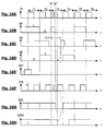
La réponse du circuit DCT1 aux quatre types d'injection d'erreur mentionnés plus haut est illustrée par les
Dans l'exemple illustré par les
Le passage à 0 du signal d'erreur synchrone SERS étant transitoire, il doit être détecté et exploité en temps réel par un circuit de protection associé, ou par un sous-programme d'interruption, comme décrit plus loin, afin de provoquer une réaction immédiate visant la protection du circuit synchrone sous surveillance ou des organes qu'il contrôle.The transition to 0 of the synchronous error signal SERS being transient, it must be detected and exploited in real time by an associated protection circuit, or by an interrupt routine, as described below, in order to provoke a reaction. immediately to protect the synchronous circuit under surveillance or the organs it controls.
Dans l'exemple illustré par les
Dans l'exemple illustré par les
Dans l'exemple illustré par les
Il ressort de ces chronogrammes que le retard DLY1 détermine un seuil de détection d'un rapprochement des fronts d'horloge et détermine ainsi la sensibilité du dispositif de détection aux accélérations du signal d'horloge CK. Si le délai DLY1 est petit devant la période T du signal d'horloge, certaines accélérations ne seront pas détectées. En pratique, et dans le cadre de l'application de l'invention à la surveillance du signal d'horloge d'un circuit synchrone, le retard DLY1 est de préférence égal au temps de propagation le plus long d'une donnée dans le circuit synchrone. Comme indiqué plus haut, ce temps de propagation le plus long est le temps de propagation le plus long d'une donnée à travers un chemin asynchrone reliant deux éléments synchrones.It emerges from these timing diagrams that the delay DLY1 determines a detection threshold of a convergence of the clock fronts and thus determines the sensitivity of the detection device to the accelerations of the clock signal CK. If the delay DLY1 is small in front of the period T of the clock signal, certain accelerations will not be detected. In practice, and in the context of the application of the invention to the monitoring of the clock signal of a synchronous circuit, the delay DLY1 is preferably equal to the longest propagation time of a datum in the circuit synchronous. As indicated above, this longest propagation time is the longest propagation time of a data through an asynchronous path connecting two synchronous elements.
Le dispositif de détection selon l'invention est susceptible de diverses variantes et modes de réalisation.The detection device according to the invention is capable of various variants and embodiments.
La
D'autres variantes de ce type peuvent être prévues par l'homme de l'art, par exemple en appliquant le signal INIT à l'entrée RST de chaque bascule.Other variants of this type may be provided by those skilled in the art, for example by applying the INIT signal to the RST input of each flip-flop.
La
Le circuit DLG2 est prévu pour éviter une auto-oscillation de la bascule FFB pendant les périodes de commutation, en raison du rebouclage de la sortie /Q sur l'entrée D. Selon la structure de la bascule FFB et son temps de commutation, le circuit DLG2 peut n'être pas nécessaire. Dans ce cas le délai DLY2 est nul.The circuit DLG2 is provided to prevent self-oscillation of the FFB during switching periods, due to the loopback of the output / Q on the input D. According to the structure of the flip-flop FFB and its switching time, the DLG2 circuit may not be necessary. In this case the delay DLY2 is zero.
Bien que découplées, les bascules FFA, FFB fonctionnent de façon sensiblement similaire à ce qui a été décrit plus haut, le couple de bits de contrôle QA et QB passant alternativement de la valeur 01 à la valeur 10 et de la valeur 10 à la valeur 01 et présentant une valeur erronée 00 ou 11 en cas d'accélération du signal d'horloge.Although decoupled, the FFA, FFB flip-flops operate in a manner substantially similar to that described above, the pair of control bits QA and QB alternately passing from the value 01 to the value 10 and from the value 10 to the value 01 and presenting a erroneous value 00 or 11 in the case of acceleration of the clock signal.
Par ailleurs, en raison du découplage des bits de contrôle QA, QB, la valeur initiale du mot de contrôle n'est pas nécessairement 01 ou 10. La valeur initiale peut être 11 ou 00. Dans ce cas la porte XOR1 dans le circuit de surveillance WCT est remplacée par une porte NON OU EXCLUSIF afin de détecter les couples de valeur 01 et 10 comme représentatifs d'une accélération interdite du signal d'horloge. Il apparaît toutefois, après étude préliminaire, que la configuration "00" ou "11" du mot de contrôle pourrait ne pas permettre de détecter certaines attaques. Le meilleur mode de réalisation de l'invention semble donc celui qui utilise des valeurs inversées "01" ou "10" du mot de contrôle.Moreover, because of the decoupling of the control bits QA, QB, the initial value of the control word is not necessarily 01 or 10. The initial value can be 11 or 00. In this case the gate XOR1 in the circuit of WCT monitoring is replaced by a NON OR EXCLUSIVE gate to detect the pairs of values 01 and 10 as representative of a prohibited acceleration of the clock signal. It appears however, after preliminary study, that the configuration "00" or "11" of the control word could not allow to detect certain attacks. The best embodiment of the invention thus seems to be one that uses inverted values "01" or "10" of the control word.
Il apparaîtra clairement à l'homme de l'art que le dispositif de détection selon l'invention est susceptible de diverses autres variantes et modes de réalisation. Ainsi, bien que l'on ait décrit dans ce qui précède des modes de réalisation dans lesquels le nombre de bascules du registre à décalage est réduit au minimum, le nombre de bascules peut au contraire être maximal si aucune contrainte d'encombrement n'est imposée au concepteur. Le registre à décalage selon l'invention peut comprendre des bascules redondantes, par exemple quatre bascules en cascade recevant à l'initialisation des bits de contrôle égaux à 0101 et formant un mot de contrôle dont les valeurs successives sont 0101 et 1010.It will be clear to one skilled in the art that the detection device according to the invention is susceptible of various other variants and embodiments. Thus, although in the foregoing embodiments have been described in which the number of latches of the shift register is reduced to a minimum, the number of flip-flops can on the contrary be maximum if no congestion constraint is required. imposed on the designer. The shift register according to the invention may comprise redundant flip-flops, for example four cascaded flip-flops receiving on initialization control bits equal to 0101 and forming a control word whose successive values are 0101 and 1010.
Par ailleurs, l'utilisation de bascules synchrones du type décrit plus haut n'est pas indispensable pour la mise en oeuvre de l'invention. Le registre à décalage pourrait être réalisé par exemple à partir d'une mémoire volatile (mémoire RAM) contrôlée par un circuit logique cadencé par le signal d'horloge à surveiller qui fait transiter les bits du mot de contrôle d'une cellule mémoire à l'autre à chaque cycle d'horloge (avec application du retard DLY1 à la transition d'un bit de contrôle sur deux), ou qui inverse la valeur de chaque bit de contrôle à chaque cycle d'horloge (en appliquant le retard DLY1 à l'inversion d'un bit de contrôle sur deux).Moreover, the use of synchronous flip-flops of the type described above is not essential for the implementation of the invention. The shift register could be made for example from a volatile memory (RAM memory) controlled by a logic circuit clocked by the clock signal to be monitored which passes the bits of the control word of a memory cell to the every other clock cycle (with application of the delay DLY1 to the transition of one control bit in two), or which inverts the value of each control bit at each clock cycle (by applying the delay DLY1 to the inversion of a control bit on two).
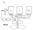
La présente invention est également susceptible de diverses applications. Sur la
La
Le circuit intégré est équipé d'un circuit DCT selon l'invention, assurant la détection des accélérations du signal d'horloge CK. Le circuit DCT reçoit par exemple le signal CK prélevé à la sortie du circuit INTCT. Le circuit DCT fournit le signal d'erreur synchrone SERS qui est envoyé à l'unité centrale pour prendre des mesures d'urgence en réponse au passage du signal SERS à la valeur active. Ces mesures d'urgence peuvent être exécutées par un circuit de protection à logique câblée spécifiquement prévu à cet effet, qui peut par exemple provoquer une remise à zéro hardware de l'unité centrale, un effacement, une destruction ou un verrouillage de certaines parties du plan mémoire, etc. Les mesures d'urgence peuvent également être traitées par l'unité centrale en faisant basculer celle-ci dans un sous-programme dédié. Dans ce cas, et comme représenté, le signal d'erreur SERS est appliqué à un décodeur d'interruption ITDEC qui fournit à l'unité centrale UC un vecteur d'interruption ITV lorsque le signal d'erreur SERS présente la valeur active.The integrated circuit is equipped with a DCT circuit according to the invention, ensuring the detection of accelerations of the clock signal CK. The DCT circuit receives, for example, the signal CK taken at the output of the circuit INTCT. The DCT circuit provides the SERS synchronous error signal which is sent to the central unit to take emergency measures in response to the passage of the SERS signal to the active value. These emergency measures can be carried out by a specially designed hard-wired logic protection circuit, which can for example cause a hardware reset of the central unit, an erasure, destruction or locking of certain parts of the system. memory map, etc. The emergency measures can also be processed by the central unit by switching it in a dedicated routine. In this case, and as shown, the SERS error signal is applied to an ITDEC interrupt decoder which provides the CPU with an ITV interrupt vector when the SERS error signal has the active value.
La présente invention est également susceptible de diverses applications autres que la surveillance d'un signal d'horloge et est applicable de façon générale à la surveillance de l'intégrité de tout type de signal logique, périodique ou non. Par exemple, lorsque des données sont envoyées à plusieurs éléments à travers un arbre de données, un dispositif de détection selon l'invention peut être utilisé pour détecter une corruption de données dans l'arbre de données par injection d'un créneau positif ou négatif, retard ou avance d'un front.The present invention is also capable of various applications other than the monitoring of a clock signal and is generally applicable to monitoring the integrity of any type of logic signal, periodic or otherwise. For example, when data are sent to several elements through a data tree, a detection device according to the invention can be used to detect a data corruption in the data tree by injecting a positive or negative slot, delay or advance 'a forehead.
Claims (21)
Applications Claiming Priority (1)
| Application Number | Priority Date | Filing Date | Title |
|---|---|---|---|
| FR0700594A FR2911979A1 (en) | 2007-01-29 | 2007-01-29 | Logic signal's i.e. clock signal, parasite acceleration detecting method for integrated circuit of e.g. chip card, involves determining acceleration when check bits do not have their respective initial or inversed values, simultaneously |
Publications (2)
| Publication Number | Publication Date |
|---|---|
| EP1986137A2 true EP1986137A2 (en) | 2008-10-29 |
| EP1986137A3 EP1986137A3 (en) | 2009-11-18 |
Family
ID=38657335
Family Applications (1)
| Application Number | Title | Priority Date | Filing Date |
|---|---|---|---|
| EP08000427A Withdrawn EP1986137A3 (en) | 2007-01-29 | 2008-01-11 | Method and device for checking the integrity of a logical signal, in particular a clock signal |
Country Status (3)
| Country | Link |
|---|---|
| US (1) | US8412996B2 (en) |
| EP (1) | EP1986137A3 (en) |
| FR (1) | FR2911979A1 (en) |
Families Citing this family (5)
| Publication number | Priority date | Publication date | Assignee | Title |
|---|---|---|---|---|
| US8255702B1 (en) * | 2009-12-03 | 2012-08-28 | Altera Corporation | Programmable logic device with improved security |
| US8378710B1 (en) | 2011-09-20 | 2013-02-19 | Nxp B.V. | Secure device anti-tampering circuit |
| EP2854292B1 (en) * | 2013-09-30 | 2016-04-20 | Nxp B.V. | Variability resistant circuit element and signal processing method |
| US9647653B2 (en) | 2015-06-04 | 2017-05-09 | Apple Inc. | Method for reduced power clock frequency monitoring |
| DE102016118534A1 (en) * | 2016-09-29 | 2018-03-29 | Infineon Technologies Ag | Circuit and method for checking the integrity of a control signal |
Citations (3)
| Publication number | Priority date | Publication date | Assignee | Title |
|---|---|---|---|---|
| US5619155A (en) * | 1995-06-02 | 1997-04-08 | United Microelectronics Corporation | IC-chip operation inhibitor |
| GB2347566A (en) * | 1999-03-01 | 2000-09-06 | Motorola Ltd | Detection of excessive clock frequency |
| EP1054345A2 (en) * | 1999-05-20 | 2000-11-22 | Beta Research GmbH | Digital analysis of the external clock frequency of chipcards |
-
2007
- 2007-01-29 FR FR0700594A patent/FR2911979A1/en not_active Withdrawn
-
2008
- 2008-01-11 EP EP08000427A patent/EP1986137A3/en not_active Withdrawn
- 2008-01-28 US US12/020,812 patent/US8412996B2/en active Active
Patent Citations (3)
| Publication number | Priority date | Publication date | Assignee | Title |
|---|---|---|---|---|
| US5619155A (en) * | 1995-06-02 | 1997-04-08 | United Microelectronics Corporation | IC-chip operation inhibitor |
| GB2347566A (en) * | 1999-03-01 | 2000-09-06 | Motorola Ltd | Detection of excessive clock frequency |
| EP1054345A2 (en) * | 1999-05-20 | 2000-11-22 | Beta Research GmbH | Digital analysis of the external clock frequency of chipcards |
Also Published As
| Publication number | Publication date |
|---|---|
| US8412996B2 (en) | 2013-04-02 |
| EP1986137A3 (en) | 2009-11-18 |
| FR2911979A1 (en) | 2008-08-01 |
| US20080208497A1 (en) | 2008-08-28 |
Similar Documents
| Publication | Publication Date | Title |
|---|---|---|
| EP2280364B1 (en) | Faults injection detector in an integrated circuit | |
| EP1993057B1 (en) | Detection of a status disruption of a flip-flop of an electronic circuit | |
| US7525836B2 (en) | Non-imprinting memory with high speed erase | |
| EP1986137A2 (en) | Method and device for checking the integrity of a logical signal, in particular a clock signal | |
| EP3033831B1 (en) | Functional timing sensors | |
| FR2929470A1 (en) | METHOD FOR PROTECTING PROGRAMMABLE CRYPTOGRAPHIC CIRCUIT, AND CIRCUIT PROTECTED BY SUCH A METHOD | |
| EP0875830A1 (en) | Testable circuit with reduced pin count | |
| EP3712794A1 (en) | Method for executing a binary code of a function secured by a microprocessor | |
| EP1950577A2 (en) | Method for verifying the integrity of a clock tree | |
| EP0884704B1 (en) | Integrated circuit authentication method | |
| EP1417582B1 (en) | Electronic circuit assembly comprising means for decontaminating error-contaminated parts | |
| EP1939745B1 (en) | Method and device for securing the reading of a memory | |
| EP1880387B1 (en) | Device for protecting a memory against fault-injection attacks | |
| FR2889005A1 (en) | PERMANENT MATERIAL INTEGRITY OF DATA | |
| FR2884000A1 (en) | Cryptographic coprocessor control execution monitoring method for integrated circuit, involves carrying error signal if abnormal flow of execution is detected and preventing access to register as long as signal is given with active value | |
| EP1571522A1 (en) | Device for protecting against error injection in an asynchronous logical block from an elementary logical module | |
| EP1571754B1 (en) | Device for protecting a synchronous flip-flop of an elementary logic module against intrusion of errors | |
| EP2424110B1 (en) | Securisation of an element for storing binary data, check register and a smart card | |
| EP1818677B1 (en) | Electronic circuit comprising a test mode secured by breaking a scan chain | |
| WO2003032160A2 (en) | Circuit architecture protected against perturbations | |
| EP1742075A1 (en) | Test method for an electronic circuit comprising a signature-based secure test mode and associated electronic circuit. | |
| EP1589395A1 (en) | Microprocessor comprising signing means for detecting an error injection attack |
Legal Events
| Date | Code | Title | Description |
|---|---|---|---|
| PUAI | Public reference made under article 153(3) epc to a published international application that has entered the european phase |
Free format text: ORIGINAL CODE: 0009012 |
|
| AK | Designated contracting states |
Kind code of ref document: A2 Designated state(s): AT BE BG CH CY CZ DE DK EE ES FI FR GB GR HR HU IE IS IT LI LT LU LV MC MT NL NO PL PT RO SE SI SK TR |
|
| AX | Request for extension of the european patent |
Extension state: AL BA MK RS |
|
| PUAL | Search report despatched |
Free format text: ORIGINAL CODE: 0009013 |
|
| AK | Designated contracting states |
Kind code of ref document: A3 Designated state(s): AT BE BG CH CY CZ DE DK EE ES FI FR GB GR HR HU IE IS IT LI LT LU LV MC MT NL NO PL PT RO SE SI SK TR |
|
| AX | Request for extension of the european patent |
Extension state: AL BA MK RS |
|
| 17P | Request for examination filed |
Effective date: 20100409 |
|
| 17Q | First examination report despatched |
Effective date: 20100527 |
|
| AKX | Designation fees paid |
Designated state(s): DE FR GB IT |
|
| STAA | Information on the status of an ep patent application or granted ep patent |
Free format text: STATUS: THE APPLICATION IS DEEMED TO BE WITHDRAWN |
|
| 18D | Application deemed to be withdrawn |
Effective date: 20120801 |