EP1986039A2 - Liquid crystal display device and driving method thereof - Google Patents
Liquid crystal display device and driving method thereof Download PDFInfo
- Publication number
- EP1986039A2 EP1986039A2 EP07150401A EP07150401A EP1986039A2 EP 1986039 A2 EP1986039 A2 EP 1986039A2 EP 07150401 A EP07150401 A EP 07150401A EP 07150401 A EP07150401 A EP 07150401A EP 1986039 A2 EP1986039 A2 EP 1986039A2
- Authority
- EP
- European Patent Office
- Prior art keywords
- viewing angle
- subpixels
- liquid crystal
- electrode
- voltage
- Prior art date
- Legal status (The legal status is an assumption and is not a legal conclusion. Google has not performed a legal analysis and makes no representation as to the accuracy of the status listed.)
- Granted
Links
Images






Classifications
-
- G—PHYSICS
- G02—OPTICS
- G02F—OPTICAL DEVICES OR ARRANGEMENTS FOR THE CONTROL OF LIGHT BY MODIFICATION OF THE OPTICAL PROPERTIES OF THE MEDIA OF THE ELEMENTS INVOLVED THEREIN; NON-LINEAR OPTICS; FREQUENCY-CHANGING OF LIGHT; OPTICAL LOGIC ELEMENTS; OPTICAL ANALOGUE/DIGITAL CONVERTERS
- G02F1/00—Devices or arrangements for the control of the intensity, colour, phase, polarisation or direction of light arriving from an independent light source, e.g. switching, gating or modulating; Non-linear optics
- G02F1/01—Devices or arrangements for the control of the intensity, colour, phase, polarisation or direction of light arriving from an independent light source, e.g. switching, gating or modulating; Non-linear optics for the control of the intensity, phase, polarisation or colour
- G02F1/13—Devices or arrangements for the control of the intensity, colour, phase, polarisation or direction of light arriving from an independent light source, e.g. switching, gating or modulating; Non-linear optics for the control of the intensity, phase, polarisation or colour based on liquid crystals, e.g. single liquid crystal display cells
- G02F1/133—Constructional arrangements; Operation of liquid crystal cells; Circuit arrangements
- G02F1/1333—Constructional arrangements; Manufacturing methods
- G02F1/1343—Electrodes
- G02F1/134309—Electrodes characterised by their geometrical arrangement
-
- G—PHYSICS
- G02—OPTICS
- G02F—OPTICAL DEVICES OR ARRANGEMENTS FOR THE CONTROL OF LIGHT BY MODIFICATION OF THE OPTICAL PROPERTIES OF THE MEDIA OF THE ELEMENTS INVOLVED THEREIN; NON-LINEAR OPTICS; FREQUENCY-CHANGING OF LIGHT; OPTICAL LOGIC ELEMENTS; OPTICAL ANALOGUE/DIGITAL CONVERTERS
- G02F1/00—Devices or arrangements for the control of the intensity, colour, phase, polarisation or direction of light arriving from an independent light source, e.g. switching, gating or modulating; Non-linear optics
- G02F1/01—Devices or arrangements for the control of the intensity, colour, phase, polarisation or direction of light arriving from an independent light source, e.g. switching, gating or modulating; Non-linear optics for the control of the intensity, phase, polarisation or colour
- G02F1/13—Devices or arrangements for the control of the intensity, colour, phase, polarisation or direction of light arriving from an independent light source, e.g. switching, gating or modulating; Non-linear optics for the control of the intensity, phase, polarisation or colour based on liquid crystals, e.g. single liquid crystal display cells
- G02F1/133—Constructional arrangements; Operation of liquid crystal cells; Circuit arrangements
- G02F1/1333—Constructional arrangements; Manufacturing methods
- G02F1/1343—Electrodes
-
- G—PHYSICS
- G02—OPTICS
- G02F—OPTICAL DEVICES OR ARRANGEMENTS FOR THE CONTROL OF LIGHT BY MODIFICATION OF THE OPTICAL PROPERTIES OF THE MEDIA OF THE ELEMENTS INVOLVED THEREIN; NON-LINEAR OPTICS; FREQUENCY-CHANGING OF LIGHT; OPTICAL LOGIC ELEMENTS; OPTICAL ANALOGUE/DIGITAL CONVERTERS
- G02F1/00—Devices or arrangements for the control of the intensity, colour, phase, polarisation or direction of light arriving from an independent light source, e.g. switching, gating or modulating; Non-linear optics
- G02F1/01—Devices or arrangements for the control of the intensity, colour, phase, polarisation or direction of light arriving from an independent light source, e.g. switching, gating or modulating; Non-linear optics for the control of the intensity, phase, polarisation or colour
- G02F1/13—Devices or arrangements for the control of the intensity, colour, phase, polarisation or direction of light arriving from an independent light source, e.g. switching, gating or modulating; Non-linear optics for the control of the intensity, phase, polarisation or colour based on liquid crystals, e.g. single liquid crystal display cells
- G02F1/1323—Arrangements for providing a switchable viewing angle
-
- G—PHYSICS
- G02—OPTICS
- G02F—OPTICAL DEVICES OR ARRANGEMENTS FOR THE CONTROL OF LIGHT BY MODIFICATION OF THE OPTICAL PROPERTIES OF THE MEDIA OF THE ELEMENTS INVOLVED THEREIN; NON-LINEAR OPTICS; FREQUENCY-CHANGING OF LIGHT; OPTICAL LOGIC ELEMENTS; OPTICAL ANALOGUE/DIGITAL CONVERTERS
- G02F1/00—Devices or arrangements for the control of the intensity, colour, phase, polarisation or direction of light arriving from an independent light source, e.g. switching, gating or modulating; Non-linear optics
- G02F1/01—Devices or arrangements for the control of the intensity, colour, phase, polarisation or direction of light arriving from an independent light source, e.g. switching, gating or modulating; Non-linear optics for the control of the intensity, phase, polarisation or colour
- G02F1/13—Devices or arrangements for the control of the intensity, colour, phase, polarisation or direction of light arriving from an independent light source, e.g. switching, gating or modulating; Non-linear optics for the control of the intensity, phase, polarisation or colour based on liquid crystals, e.g. single liquid crystal display cells
- G02F1/133—Constructional arrangements; Operation of liquid crystal cells; Circuit arrangements
- G02F1/1333—Constructional arrangements; Manufacturing methods
- G02F1/1337—Surface-induced orientation of the liquid crystal molecules, e.g. by alignment layers
-
- G—PHYSICS
- G02—OPTICS
- G02F—OPTICAL DEVICES OR ARRANGEMENTS FOR THE CONTROL OF LIGHT BY MODIFICATION OF THE OPTICAL PROPERTIES OF THE MEDIA OF THE ELEMENTS INVOLVED THEREIN; NON-LINEAR OPTICS; FREQUENCY-CHANGING OF LIGHT; OPTICAL LOGIC ELEMENTS; OPTICAL ANALOGUE/DIGITAL CONVERTERS
- G02F1/00—Devices or arrangements for the control of the intensity, colour, phase, polarisation or direction of light arriving from an independent light source, e.g. switching, gating or modulating; Non-linear optics
- G02F1/01—Devices or arrangements for the control of the intensity, colour, phase, polarisation or direction of light arriving from an independent light source, e.g. switching, gating or modulating; Non-linear optics for the control of the intensity, phase, polarisation or colour
- G02F1/13—Devices or arrangements for the control of the intensity, colour, phase, polarisation or direction of light arriving from an independent light source, e.g. switching, gating or modulating; Non-linear optics for the control of the intensity, phase, polarisation or colour based on liquid crystals, e.g. single liquid crystal display cells
- G02F1/133—Constructional arrangements; Operation of liquid crystal cells; Circuit arrangements
- G02F1/1333—Constructional arrangements; Manufacturing methods
- G02F1/1337—Surface-induced orientation of the liquid crystal molecules, e.g. by alignment layers
- G02F1/133707—Structures for producing distorted electric fields, e.g. bumps, protrusions, recesses, slits in pixel electrodes
-
- G—PHYSICS
- G02—OPTICS
- G02F—OPTICAL DEVICES OR ARRANGEMENTS FOR THE CONTROL OF LIGHT BY MODIFICATION OF THE OPTICAL PROPERTIES OF THE MEDIA OF THE ELEMENTS INVOLVED THEREIN; NON-LINEAR OPTICS; FREQUENCY-CHANGING OF LIGHT; OPTICAL LOGIC ELEMENTS; OPTICAL ANALOGUE/DIGITAL CONVERTERS
- G02F1/00—Devices or arrangements for the control of the intensity, colour, phase, polarisation or direction of light arriving from an independent light source, e.g. switching, gating or modulating; Non-linear optics
- G02F1/01—Devices or arrangements for the control of the intensity, colour, phase, polarisation or direction of light arriving from an independent light source, e.g. switching, gating or modulating; Non-linear optics for the control of the intensity, phase, polarisation or colour
- G02F1/13—Devices or arrangements for the control of the intensity, colour, phase, polarisation or direction of light arriving from an independent light source, e.g. switching, gating or modulating; Non-linear optics for the control of the intensity, phase, polarisation or colour based on liquid crystals, e.g. single liquid crystal display cells
- G02F1/137—Devices or arrangements for the control of the intensity, colour, phase, polarisation or direction of light arriving from an independent light source, e.g. switching, gating or modulating; Non-linear optics for the control of the intensity, phase, polarisation or colour based on liquid crystals, e.g. single liquid crystal display cells characterised by the electro-optical or magneto-optical effect, e.g. field-induced phase transition, orientation effect, guest-host interaction or dynamic scattering
- G02F1/139—Devices or arrangements for the control of the intensity, colour, phase, polarisation or direction of light arriving from an independent light source, e.g. switching, gating or modulating; Non-linear optics for the control of the intensity, phase, polarisation or colour based on liquid crystals, e.g. single liquid crystal display cells characterised by the electro-optical or magneto-optical effect, e.g. field-induced phase transition, orientation effect, guest-host interaction or dynamic scattering based on orientation effects in which the liquid crystal remains transparent
- G02F1/1393—Devices or arrangements for the control of the intensity, colour, phase, polarisation or direction of light arriving from an independent light source, e.g. switching, gating or modulating; Non-linear optics for the control of the intensity, phase, polarisation or colour based on liquid crystals, e.g. single liquid crystal display cells characterised by the electro-optical or magneto-optical effect, e.g. field-induced phase transition, orientation effect, guest-host interaction or dynamic scattering based on orientation effects in which the liquid crystal remains transparent the birefringence of the liquid crystal being electrically controlled, e.g. ECB-, DAP-, HAN-, PI-LC cells
-
- G—PHYSICS
- G02—OPTICS
- G02F—OPTICAL DEVICES OR ARRANGEMENTS FOR THE CONTROL OF LIGHT BY MODIFICATION OF THE OPTICAL PROPERTIES OF THE MEDIA OF THE ELEMENTS INVOLVED THEREIN; NON-LINEAR OPTICS; FREQUENCY-CHANGING OF LIGHT; OPTICAL LOGIC ELEMENTS; OPTICAL ANALOGUE/DIGITAL CONVERTERS
- G02F1/00—Devices or arrangements for the control of the intensity, colour, phase, polarisation or direction of light arriving from an independent light source, e.g. switching, gating or modulating; Non-linear optics
- G02F1/01—Devices or arrangements for the control of the intensity, colour, phase, polarisation or direction of light arriving from an independent light source, e.g. switching, gating or modulating; Non-linear optics for the control of the intensity, phase, polarisation or colour
- G02F1/13—Devices or arrangements for the control of the intensity, colour, phase, polarisation or direction of light arriving from an independent light source, e.g. switching, gating or modulating; Non-linear optics for the control of the intensity, phase, polarisation or colour based on liquid crystals, e.g. single liquid crystal display cells
- G02F1/133—Constructional arrangements; Operation of liquid crystal cells; Circuit arrangements
- G02F1/1333—Constructional arrangements; Manufacturing methods
- G02F1/1343—Electrodes
- G02F1/134309—Electrodes characterised by their geometrical arrangement
- G02F1/134345—Subdivided pixels, e.g. for grey scale or redundancy
-
- G—PHYSICS
- G02—OPTICS
- G02F—OPTICAL DEVICES OR ARRANGEMENTS FOR THE CONTROL OF LIGHT BY MODIFICATION OF THE OPTICAL PROPERTIES OF THE MEDIA OF THE ELEMENTS INVOLVED THEREIN; NON-LINEAR OPTICS; FREQUENCY-CHANGING OF LIGHT; OPTICAL LOGIC ELEMENTS; OPTICAL ANALOGUE/DIGITAL CONVERTERS
- G02F1/00—Devices or arrangements for the control of the intensity, colour, phase, polarisation or direction of light arriving from an independent light source, e.g. switching, gating or modulating; Non-linear optics
- G02F1/01—Devices or arrangements for the control of the intensity, colour, phase, polarisation or direction of light arriving from an independent light source, e.g. switching, gating or modulating; Non-linear optics for the control of the intensity, phase, polarisation or colour
- G02F1/13—Devices or arrangements for the control of the intensity, colour, phase, polarisation or direction of light arriving from an independent light source, e.g. switching, gating or modulating; Non-linear optics for the control of the intensity, phase, polarisation or colour based on liquid crystals, e.g. single liquid crystal display cells
- G02F1/133—Constructional arrangements; Operation of liquid crystal cells; Circuit arrangements
- G02F1/1333—Constructional arrangements; Manufacturing methods
- G02F1/1343—Electrodes
- G02F1/134309—Electrodes characterised by their geometrical arrangement
- G02F1/134381—Hybrid switching mode, i.e. for applying an electric field with components parallel and orthogonal to the substrates
Definitions
- the present disclosure relates to a liquid crystal display (LCD) device and a driving method thereof, and more particularly, to an LCD device that can control a viewing angle and improve brightness of an image, and a driving method thereof.
- LCD liquid crystal display
- liquid crystals have dielectric anisotropy and refractive index anisotropy
- the arrangement of the LCs is controlled according to an electric field applied thereto, and the polarization of light changes according to the arrangement.
- the LCD device applies an electric field to LCs having dielectric anisotropy and refractive index anisotropy to control light transmittance, thereby displaying an image.
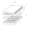
- Fig. 1 is a view of a related art LCD device.
- the LCD device includes an upper substrate 11 including a color filter array 19, and a lower substrate 1 including a thin film transistor (TFT) array 9, the upper substrate 11 and the lower substrate 1 being attached to face each other, and LCs 16 filling cell gaps disposed between the two substrates 11 and 1.
- TFT thin film transistor
- the color filter array 19 includes a black matrix 12, a color filter layer 13, an overcoat layer 14 for planarizing the upper substrate 11, and a common electrode 15 for forming an electric field in cooperation with a pixel electrode 7.
- the color filter array 19 further includes an upper alignment layer for uniformly aligning the LCs 16.
- the TFT array 9 includes gate lines 2 and data lines 3 crossing each other to define pixels on the lower substrate 1, a TFT 6 connected to the gate line 2 and the data line 3, and the pixel electrode 7 connected to the TFT 6.
- the TFT array 9 further includes a lower alignment layer for uniformly aligning the LCs 16.
- the TFT 6 supplies a data signal from the data line 3 to the pixel electrode 7 in response to a gate signal from the gate line 2.
- An electric field is generated between the pixel electrode 3 to which the data signal has been supplied through the TFT 6, and the common electrode 15 to which a reference voltage has been supplied.
- the light transmittance of the LCs 16 arranged between the lower substrate 1 and the upper substrate 11 is controlled by this electric field, so that an image is displayed.
- the LCD device has been developed in an aspect of improving a viewing angle characteristic so that an image can be viewed in any direction.
- an excellent viewing angle characteristic causes a side effect such as private information leakage in the case where a computer system is used for a private purpose or security-oriented businesses such as tasks at a bank are performed.
- an LCD device that can selectively control a viewing angle is required. That is, development of the LCD providing a wide viewing angle mode allowing an image to be viewed to a user at various viewing angles, and providing a narrow viewing angle mode limiting displaying of an image to a user at a specific viewing angle, is required.
- Embodiments provide an LCD device that can control a viewing angle and a driving method thereof.
- Embodiments also provide an LCD device that improves brightness of an image and a driving method thereof.
- a liquid crystal display device includes: data displaying subpixels where a liquid crystal layer of a vertical alignment mode using negative liquid crystals is interposed between a first pixel electrode to which red, green, and blue data voltages are applied, and a common electrode to which a common voltage is applied; and a viewing angle controlling subpixel including the liquid crystal layer of the vertical alignment mode driven in response to a voltage applied to the common electrode, a side electrode separated from the common electrode, and a second pixel electrode, each of the subpixels including a rib distorting an electric field applied to the liquid crystal layer, and the viewing angle controlling subpixel substantially directly passing light from the data displaying subpixels when an equivalent voltage to the common voltage is applied to the side electrode during a wide viewing angle mode, and delaying phase of the light from the data displaying subpixels when a voltage having a voltage difference from the common voltage is applied to the side electrode during a narrow viewing angle mode.
- a method for driving a liquid crystal display device includes: applying a common voltage to data displaying subpixels and applying a voltage having substantially the same potential as that of the common voltage to a side electrode of a viewing angle controlling subpixel to substantially directly pass light from the data displaying subpixels through the viewing angle controlling subpixel during a wide viewing angle mode; and applying the common voltage to the data displaying subpixels and applying a voltage having a voltage difference from the common voltage to the side electrode of the viewing angle controlling subpixel to delaying, at the viewing angle controlling subpixel, phase of light from the data displaying subpixels during a narrow viewing angle mode, the data displaying subpixels including a liquid crystal layer of a vertical alignment mode using negative liquid crystals between a first electrode to which red, green, and blue data voltages are applied, and a common electrode to which the common voltage is applied, and the viewing angle controlling subpixel including the liquid crystal layer of the vertical alignment mode driven in response to a voltage applied to the common electrode, a side electrode separated from the common electrode, and a second
- Fig. 1 is a view of a related art LCD device.
- Fig. 2 is a plan view illustrating a TFT array of an LCD device according to an embodiment.
- Fig. 3 is a cross-sectional view of a TFT taken along the line I-I' of Fig. 2 .
- Fig. 4 is a plan view illustrating a color filter array of an LCD device according to an embodiment.
- Fig. 5 is a cross-sectional view of a color filter array taken along the lines I-I' and II-II' of Fig. 4 .
- Fig. 6 is a view explaining an LCD device in a no voltage application state.
- Figs. 7A and 7B are views explaining a wide viewing angle mode of an LCD device according to an embodiment.
- Figs. 8A and 8B are views explaining a narrow viewing angle mode of an LCD device according to an embodiment.
- any reference in this specification to "one embodiment,” “an embodiment,” “example embodiment,” etc. means that a particular feature, structure, or characteristic described in connection with the embodiment is included in at least one embodiment of the invention.
- the appearances of such phrases in various places in the specification are not necessarily all referring to the same embodiment.
- An LCD device is formed by attaching a first substrate including a TFT array, and a second substrate including a color filter array such that those arrays face each other.
- An LC layer is interposed between the first and second substrates.
- Fig. 2 is a plan view illustrating a TFT array according to an embodiment
- Fig. 3 is a cross-sectional view taken along the line I-I' of Fig. 2
- the line I-I' is a line representing a horizontal direction of a display surface.
- the TFT array includes a plurality of pixels formed on the first substrate.
- the pixels include subpixels Pr, Pg, Pb, and Pv defined by crossing of a plurality of gate lines 112 and a plurality of data lines 115.
- One pixel includes data displaying subpixels Pr, Pg, and Pb for realizing red (R), green (G), and blue (B) pixels, respectively, and a viewing angle controlling subpixel Pv for controlling a viewing angle.
- the data displaying subpixels Pr, Pg, and Pb include a TFT connected to a crossing of the gate line 112 and the data line 115, and a first pixel electrode 117 connected to the TFT.
- the viewing angle controlling subpixel Pv includes a TFT connected to a crossing of the gate line 112 and the data line 115, and a second pixel electrode 517 connected to the TFT.
- the gate line 112 and the data line 115 cross each other such that they are insulated from each other with a gate insulating layer 113 interposed.
- the gate line 112 supplies a scan voltage to the TFT
- the data line 115 supplies a data voltage to the TFT.
- the TFTs of the data displaying subpixels Pr, Pg, and Pb allow R, G, and B data voltages of the data line 115 to charge the first pixel electrode 117 in response to a scan voltage of the gate line 112.
- the TFTs of the data displaying subpixels Pr, Pg, and Pb include a gate electrode 112a branching from the gate line 112, a source electrode 115a branching from the data line 115, and a drain electrode 115b connected to the first pixel electrode 117.
- a semiconductor pattern 114 ohmic-contacts the source electrode 115a and the drain electrode 115b.
- the data line 115 and the semiconductor pattern 114 are protected by a passivation layer 116 covering them.
- the first electrode 117 is connected to the drain electrode 115b through a first contact hole 119 passing through the gate insulating layer 113 and exposing the drain electrode 115b.
- R, G, and B data voltages passing through the TFTs of the data displaying subpixels Pr, Pg, and Pb are supplied to the first pixel electrode 117. Accordingly, a potential difference is generated between the first pixel electrode 117 and a common electrode of the color filter array. This potential difference drives LCs contained in the data displaying subpixels Pr, Pg, and Pb to realize the pixel.
- the TFT of the viewing angle controlling subpixel Pv allows a viewing angle controlling data voltage of the data line 115 to charge the second pixel electrode 517 in response to a scan voltage of the gate line 112.
- the TFT of the viewing angle controlling subpixel Pv includes a gate electrode 512a branching from the gate line 112, a source electrode 515a branching from the data line 115, and a drain electrode 515b connected to the second pixel electrode 517.
- a semiconductor pattern 514 ohmic-contacts the source electrode 515a and the drain electrode 515b.
- the data line 115 and the semiconductor pattern 514 are protected by a passivation layer 116 covering them.
- the second electrode 517 is connected to the drain electrode 515b through a second contact hole 519 passing through the gate insulating layer 113 and exposing the drain electrode 515b.
- a viewing angle controlling data voltage passing through the TFT of the viewing angle controlling subpixel Pv is supplied to the second pixel electrode 517. Accordingly, a potential difference is generated between the second pixel electrode 517 and the common electrode of the color filter array. This potential difference drives the LCs contained in the viewing angle controlling subpixel Pv to control the viewing angle and the brightness of the pixel.
- the TFT array 111 according to the embodiment can be manufactured through a plurality of mask processes including a photolithography process and an etching process.
- An example of a TFT array manufacturing method is schematically described.
- a gate conductive pattern including the gate line 112 and the gate electrodes 112a and 512a is formed on the first substrate 110.
- the gate conductive pattern can be a single layer or a multiple layer formed by stacking one or more metal such as Mo, Ti, Cu, AlNd, Al, Cr, an Mo alloy, a Cu alloy, and an Al alloy.
- the gate insulating layer 113 covering the gate conductive pattern is formed on the first substrate 110 including the gate insulating layer 113. After that, during a second mask process, a source/drain conductive pattern including the semiconductor patterns 114 and 514, the data line 115, the source electrodes 115a and 515a, and the drain electrodes 115b and 515b.
- the gate insulating layer 113 can be generally formed of an inorganic insulating material such as SiO x and SiN x .
- the semiconductor pattern can be formed in a structure where amorphous silicon and amorphous silicon doped with impurities (n+ or p+) are stacked. An amorphous silicon layer is exposed between the source electrode 115a/515a and the drain electrode 115b/515b.
- the source/drain conductive pattern can be a single layer or a multiple layer formed by stacking one or more metal such as Mo, Ti, Cu, AlNd, Al, Cr, an Mo alloy, a Cu alloy, and an Al alloy.
- the semiconductor patterns 114 and 514, and the source/drain conductive pattern can be formed through one mask process using a half tone mask or a diffraction exposure mask. Accordingly, the semiconductor patterns 114 and 514 overlap each other under the source/drain conductive pattern.
- the passivation layer 116 covering the semiconductor patterns 114 and 514 and the source/drain conductive pattern is formed on the gate insulating layer 113. Subsequently, contact holes 119 and 519 are formed during a third mask process.
- the passivation layer 116 can be formed of an inorganic insulating material such as SiO x and SiN x , or an organic insulating material such as benzo cyclobutene (BCB), perfluorocyclobutane (PFBC), Teflon, and cytop.
- an inorganic insulating material such as SiO x and SiN x
- an organic insulating material such as benzo cyclobutene (BCB), perfluorocyclobutane (PFBC), Teflon, and cytop.
- a transparent conductive pattern including the second pixel electrode 517 and the first pixel electrode 117 is formed on the passivation layer 116 through a fourth mask process.
- the transparent conductive pattern can be formed of indium-tin-oxide (ITO), tin-oxide (TO), indium-zinc-oxide (IZO), or indium-tin-zinc-oxide (ITZO).
- ITO indium-tin-oxide
- TO tin-oxide
- IZO indium-zinc-oxide
- ITZO indium-tin-zinc-oxide
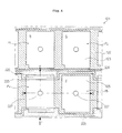
- Fig. 4 is a view illustrating a color filter array of an LCD device according to an embodiment
- Fig. 5 is a cross-sectional view taken along the lines I-I' and II-II' of Fig. 4
- the line I-I' is a line representing the horizontal direction of a display surface
- the line II-II' is a line representing a vertical direction of the display surface.
- a color filter array 121 includes a plurality of pixels formed on a second substrate 120.
- the pixel includes subpixels Pr, Pg, Pb, and Pv divided by a black matrix (BM) 122.
- One pixel includes data displaying subpixels Pr, Pg, and Pb for realizing red (R), green (G), and blue (B) pixels, respectively, and a viewing angle controlling subpixel Pv for controlling a viewing angle.
- the BM 122 divides the subpixels Pr, Pg, Pb, and Pv, and prevents generation of light leakage at regions where gate lines, data lines, and TFTs are formed, and the adjacent regions thereof of a TFT array.
- Common electrodes 225 are formed in the subpixels Pr, Pg, Pb, and Pv.
- the common electrodes 225 according to an embodiment are independently formed in pixel rows in the form of a row arrangement of the subpixels Pr, Pg, Pb, and Pv, respectively, or independently formed in pixel columns in the form of a column arrangement of the subpixels Pr, Pg, Pb, and Pv, respectively.
- the drawing for explaining the embodiment illustrates that the common electrodes 225 are independently formed in pixel rows, respectively.
- Ribs 227 and 527 formed of an organic insulating material having a low dielectric constant are formed at the centers of the subpixels Pr, Pg, Pb, and Pv.
- the ribs 227 and 527 distort an electric field formed in the subpixels Pr, Pg, Pb, and Pv to allow LCs to be symmetrically arranged with respect to the ribs 227 and 527.
- Color filter patterns 123 are formed in data displaying subpixels Pr, Pg, and Pb of the subpixels Pr, Pg, Pb, and Pv.
- the color filter patterns 123 include a red layer formed on the R subpixel Pr, a green layer formed on the G subpixel Pg, and a blue layer formed on the B subpixel Pb, and transmit R, G, and B light, respectively.
- a side electrode 520 separated from the common electrode 225 is formed in a viewing angle controlling subpixel Pv of the subpixels Pr, Pg, Pb, and Pv.
- the side electrode 520 distorts an electric field formed in the viewing angle controlling subpixel Pv to contribute to brightness improvement of the pixel during a narrow viewing angle mode.
- the side electrode 520 includes a pair of side electrodes facing each other with the common electrode 225 interposed.
- the side electrode 520 overlaps the BM 122 and connects to a control line 524 avoiding (that is, not overlapping) the data displaying subpixels Pr, Pg, and Pb to receive a control signal.
- the color filter patterns 123 and the BM 122 are covered with an overcoat layer 129.
- the overcoat layer 129 planarizes height differences generated by the forming of the BM 122 and the color filter patterns 123.
- the color filter array 121 according to the embodiment can be manufactured through a plurality of mask processes including a photolithography process and an etching process.
- An example of a color filter array manufacturing method is schematically described.
- the BM 122 is formed on the second substrate 120.
- the BM 122 can be formed of an opaque metal including Cr, or a black resin.
- the color filter patterns 123 are formed through a second mask process.
- the color filter patterns 123 can be red, green, and blue color resists.
- a second mask process includes a process of shifting a second mask to sequentially pattern the R, G, and B color resists.
- the BM 122 and the color filter pattern 123 are covered with the overcoat layer 129.
- the overcoat layer 129 can be a transparent resin.
- a transparent conductive pattern including the common electrode 225, the control line 524, and the side electrode 520 is formed on the overcoat layer 129 through a third mask process.
- the transparent conductive pattern can be formed of indium-tin-oxide (ITO), tin-oxide (TO), indium-zinc-oxide (IZO), or indium-tin-zinc-oxide (ITZO).
- ITO indium-tin-oxide
- TO tin-oxide
- IZO indium-zinc-oxide
- ITZO indium-tin-zinc-oxide
- Ribs 227 and 527 are formed on portions of the common electrode 225 corresponding to the centers of the subpixels Pr, Pg, Pb, and Pv.
- the ribs 227 and 527 are formed of an acryl-based organic compound having a low dielectric constant.
- a method for manufacturing an LCD device includes forming the TFT array 111 and the color filter array 121 described in Figs. 2 to 5 .
- the method further includes a process of attaching the first substrate 110 and the second substrate 120 to each other such that the TFT array 111 and the color filter array 121 face each other, an LC forming process, and a polarizer attaching process.
- LCs can be dropped on the TFT array 111 or the color filter array 121 before the first and second substrates 110 and 120 are attached to each other. Also, after the first and second substrates 110 and 120 are attached to each other, the LCs can be dropped in a space between the TFT array 111 and the color filter array 121.
- the LCs can be formed in various ways.
- the subpixels Pr, Pg, Pb, and Pv contained in the arrays 111 and 121 face each other, and the BM 122 of the color filter array 121 overlaps the TFT of the TFT array 111, the gate lines 112, and the data lines 115.
- the polarizer includes a first polarizer and a second polarizer attached on the outer surfaces of the two substrates, respectively.
- the transmission axes of the first polarizer and the second polarizer are perpendicular to each other.
- the LCD device includes a vertical alignment (VA) mode LC layer. That is, the LC layer according to the embodiment is a negative type LC layer having negative dielectric anisotropy, and includes LC molecules vertically aligned at an initial alignment.
- VA vertical alignment
- the LCD device display black on a screen when a signal is not applied. That is, the LCD device is in a normally black mode.
- Figs. 6 , 7A , and 8A are views explaining a viewing angle mode according to an embodiment, taken along the line I-I' representing the horizontal direction of a display surface, after a process of attaching the first and second substrates 110 and 120 to each other, an LC forming process, and a process of attaching the first and second polarizers 161 and 162.
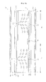
- Fig. 6 is a view illustrating an LCD device during an off-state when a voltage is not applied to the subpixels Pr, Pg, Pb, and Pv.
- the LCs 132 formed in the subpixels Pr, Pg, Pb, and Pv maintain an initial alignment state. Accordingly, the subpixels Pr, Pg, Pb, and Pv display block.
- the LCD device controls a viewing angle using the viewing angle controlling subpixel Pv when realizing an image through the data displaying subpixels Pr, Pg, and Pb. Also, the LCD device according to an embodiment improves the brightness of a unit pixel using the viewing angle controlling subpixel Pv.
- Figs. 7A and 7B are views explaining a wide viewing angle mode of an LCD device according to an embodiment.
- an image realized through the data displaying subpixels Pr, Pg, and Pb during the wide viewing angle mode is viewed not only at a front viewing angle direction but also at left and right viewing angle directions.
- the image viewed at the left and right viewing angle directions is realized by transmitting the image through the viewing angle controlling subpixel Pv in the left and right viewing angle directions.
- a common voltage is supplied to the common electrodes 225 of the subpixel Pr, Pg, and Pb.
- R, G, and B data voltages are applied to the first pixel electrodes 117 of the data displaying subpixels Pr, Pg, and Pb.
- a vertical electric field is formed between the common electrode 225 to which the common voltage has been applied, and the first pixel electrodes 117 to which the R, G, and B data voltages have been applied.
- the LCs 132 of the data displaying subpixels Pr, Pg, and Pb are driven to an alignment surface to form a right angle to the electric field, and light transmittance is controlled according to a driving state of the LCs, so that an image is displayed.
- the LCs 132 are radially distributed to be symmetrical in the vertical and horizontal directions of a display surface around the ribs 227.
- the viewing angle controlling subpixel Pv substantially directly transmits light from the data displaying subpixels Pr, Pg, and Pb in the left and right viewing angle directions, and improves the brightness of an image displayed in the front direction.
- a wide viewing angle data voltage is applied to the second electrode 517 of the viewing angle controlling subpixel Pv, and a voltage having the same potential as that of the common voltage is applied to the side electrode 520. Accordingly, a vertical electric field is generated between the second pixel electrode 517 and the common electrode 225.
- the LCs 132 contained in the viewing angle controlling subpixel Pv is driven to an alignment layer to form a right angle with the electric field. At this point, since the vertical electric field is distorted by the rib 527, the LCs 132 are radially distributed to be symmetrical in the vertical and horizontal directions of a display surface around the rib 527.
- the viewing angle controlling subpixel Pv contributes to improving the brightness of an image during the wide viewing angle mode.
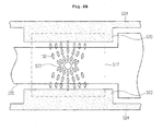
- Figs. 8A and 8B are views explaining a narrow viewing angle mode of an LCD device according to an embodiment.
- an image realized through the data displaying subpixels Pr, Pg, and Pb is displayed in the front viewing angle direction, and distorted in the left and right viewing angle directions and displayed as different information during the narrow viewing angle mode according to the embodiment.
- the image displayed in the left and right viewing angle direction is realized by transmitting light through the viewing angle controlling subpixel Pv in the left and right viewing angle direction.
- a common voltage is supplied to the common electrodes 225 of the subpixel Pr, Pg, and Pb.
- R, G, and B data voltages are applied to the first pixel electrodes 117 of the data displaying subpixels Pr, Pg, and Pb.
- a vertical electric field is formed between the common electrode 225 to which the common voltage has been applied, and the first pixel electrodes 117 to which the R, G, and B data voltages have been applied.
- the LCs 132 of the data displaying subpixels Pr, Pg, and Pb are driven to an alignment surface to form a right angle to the electric field, and light transmittance is controlled according to a driving state of the LCs, so that an image is displayed.
- the LCs 132 are radially distributed to be symmetrical in the vertical and horizontal directions of a display surface around the ribs 227.
- the viewing angle controlling subpixel Pv delays the phase of light from the data displaying subpixels Pr, Pg, and Pb in the left and right viewing angle directions, and improves the brightness of an image displayed in the front direction.
- a narrow viewing angle data voltage is applied to the second electrode 517 of the viewing angle controlling subpixel Pv, and a voltage having a potential difference with respect to the common voltage is applied to the side electrode 520. Accordingly, a vertical electric field formed between the second pixel electrode 517 and the common electrode 225 is distorted by a voltage supplied to the side electrode 520, so that the long axes of the LCs 132 are arranged such that the display surface faces the vertical direction. Simultaneously, since the electric field formed in the viewing angle controlling subpixel Pv is distorted by the rib 527, the LCs 132 are arranged to be symmetric around the rib 527.
- the viewing angle controlling subpixel Pv contributes to improving the brightness of an image during the narrow viewing angle mode.
- the degree by which the long axes of the LCs 132 are driven in the left and right viewing angle directions is controlled by a viewing angle control data voltage applied to the second pixel electrode 517, so that the wide viewing angle mode and the narrow viewing angle mode can be selectively realized.
- a light transmittance amount through the viewing angle controlling subpixel Pv in the front direction is also controlled by a voltage applied to the second pixel electrode 517.
- the LCD device controls the arrangement of the LCs using the viewing angle controlling subpixel to selectively realize the wide viewing angle mode and the narrow viewing angle mode.
- the viewing angle controlling subpixel controls the arrangement of the LCs using the ribs and the side electrode to improve brightness reduction of the pixels.
- the LCD device according to the embodiment does not require a separate viewing angle controlling panel, manufacturing costs reduce. Also, since misalignment in attaching of the viewing angle controlling panel is not generated, so that manufacturing yield can increase, and the LCD device can he manufactured in a lightweight and slim profile.
Landscapes
- Physics & Mathematics (AREA)
- Nonlinear Science (AREA)
- Chemical & Material Sciences (AREA)
- Crystallography & Structural Chemistry (AREA)
- General Physics & Mathematics (AREA)
- Optics & Photonics (AREA)
- Mathematical Physics (AREA)
- Spectroscopy & Molecular Physics (AREA)
- Geometry (AREA)
- Liquid Crystal (AREA)
- Liquid Crystal Display Device Control (AREA)
- Control Of Indicators Other Than Cathode Ray Tubes (AREA)
Abstract
Description
- The present application claims priority under 35 U.S.C. 119 and 35 U.S.C. 365 to Korean Patent Application No.
10-2007-0037940 (filed on April 18, 2007 - The present disclosure relates to a liquid crystal display (LCD) device and a driving method thereof, and more particularly, to an LCD device that can control a viewing angle and improve brightness of an image, and a driving method thereof.
- Since liquid crystals (LCs) have dielectric anisotropy and refractive index anisotropy, the arrangement of the LCs is controlled according to an electric field applied thereto, and the polarization of light changes according to the arrangement. The LCD device applies an electric field to LCs having dielectric anisotropy and refractive index anisotropy to control light transmittance, thereby displaying an image.
-
Fig. 1 is a view of a related art LCD device. - Referring to
Fig. 1 , the LCD device includes anupper substrate 11 including acolor filter array 19, and alower substrate 1 including a thin film transistor (TFT) array 9, theupper substrate 11 and thelower substrate 1 being attached to face each other, andLCs 16 filling cell gaps disposed between the twosubstrates - The
color filter array 19 includes a black matrix 12, acolor filter layer 13, anovercoat layer 14 for planarizing theupper substrate 11, and acommon electrode 15 for forming an electric field in cooperation with apixel electrode 7. Thecolor filter array 19 further includes an upper alignment layer for uniformly aligning theLCs 16. - The TFT array 9 includes gate lines 2 and
data lines 3 crossing each other to define pixels on thelower substrate 1, aTFT 6 connected to the gate line 2 and thedata line 3, and thepixel electrode 7 connected to theTFT 6. The TFT array 9 further includes a lower alignment layer for uniformly aligning theLCs 16. - The TFT 6 supplies a data signal from the
data line 3 to thepixel electrode 7 in response to a gate signal from the gate line 2. An electric field is generated between thepixel electrode 3 to which the data signal has been supplied through theTFT 6, and thecommon electrode 15 to which a reference voltage has been supplied. The light transmittance of theLCs 16 arranged between thelower substrate 1 and theupper substrate 11 is controlled by this electric field, so that an image is displayed. - The LCD device has been developed in an aspect of improving a viewing angle characteristic so that an image can be viewed in any direction. However, an excellent viewing angle characteristic causes a side effect such as private information leakage in the case where a computer system is used for a private purpose or security-oriented businesses such as tasks at a bank are performed.
- Accordingly, development of an LCD device that can selectively control a viewing angle is required. That is, development of the LCD providing a wide viewing angle mode allowing an image to be viewed to a user at various viewing angles, and providing a narrow viewing angle mode limiting displaying of an image to a user at a specific viewing angle, is required.
- Embodiments provide an LCD device that can control a viewing angle and a driving method thereof.
- Embodiments also provide an LCD device that improves brightness of an image and a driving method thereof.
- In one embodiment, a liquid crystal display device includes: data displaying subpixels where a liquid crystal layer of a vertical alignment mode using negative liquid crystals is interposed between a first pixel electrode to which red, green, and blue data voltages are applied, and a common electrode to which a common voltage is applied; and a viewing angle controlling subpixel including the liquid crystal layer of the vertical alignment mode driven in response to a voltage applied to the common electrode, a side electrode separated from the common electrode, and a second pixel electrode, each of the subpixels including a rib distorting an electric field applied to the liquid crystal layer, and the viewing angle controlling subpixel substantially directly passing light from the data displaying subpixels when an equivalent voltage to the common voltage is applied to the side electrode during a wide viewing angle mode, and delaying phase of the light from the data displaying subpixels when a voltage having a voltage difference from the common voltage is applied to the side electrode during a narrow viewing angle mode.
- In another embodiment, a method for driving a liquid crystal display device includes: applying a common voltage to data displaying subpixels and applying a voltage having substantially the same potential as that of the common voltage to a side electrode of a viewing angle controlling subpixel to substantially directly pass light from the data displaying subpixels through the viewing angle controlling subpixel during a wide viewing angle mode; and applying the common voltage to the data displaying subpixels and applying a voltage having a voltage difference from the common voltage to the side electrode of the viewing angle controlling subpixel to delaying, at the viewing angle controlling subpixel, phase of light from the data displaying subpixels during a narrow viewing angle mode, the data displaying subpixels including a liquid crystal layer of a vertical alignment mode using negative liquid crystals between a first electrode to which red, green, and blue data voltages are applied, and a common electrode to which the common voltage is applied, and the viewing angle controlling subpixel including the liquid crystal layer of the vertical alignment mode driven in response to a voltage applied to the common electrode, a side electrode separated from the common electrode, and a second pixel electrode.
- The details of one or more embodiments are set forth in the accompanying drawings and the description below. Other features will be apparent from the description and drawings, and from the claims.
-
Fig. 1 is a view of a related art LCD device. -
Fig. 2 is a plan view illustrating a TFT array of an LCD device according to an embodiment. -
Fig. 3 is a cross-sectional view of a TFT taken along the line I-I' ofFig. 2 . -
Fig. 4 is a plan view illustrating a color filter array of an LCD device according to an embodiment. -
Fig. 5 is a cross-sectional view of a color filter array taken along the lines I-I' and II-II' ofFig. 4 . -
Fig. 6 is a view explaining an LCD device in a no voltage application state. -
Figs. 7A and7B are views explaining a wide viewing angle mode of an LCD device according to an embodiment. -
Figs. 8A and8B are views explaining a narrow viewing angle mode of an LCD device according to an embodiment. - Any reference in this specification to "one embodiment," "an embodiment," "example embodiment," etc., means that a particular feature, structure, or characteristic described in connection with the embodiment is included in at least one embodiment of the invention. The appearances of such phrases in various places in the specification are not necessarily all referring to the same embodiment. Further, when a particular feature, structure, or characteristic is described in connection with any embodiment, it is submitted that it is within the purview of one skilled in the art to effect such feature, structure, or characteristic in connection with other ones of the embodiments.
- Although embodiments have been described with reference to a number of illustrative embodiments thereof, it should be understood that numerous other modifications and embodiments can be devised by those skilled in the art that will fall within the spirit and scope of the principles of this disclosure. More particularly, various variations and modifications are possible in the component parts and/or arrangements of the subject combination arrangement within the scope of the disclosure, the drawings and the appended claims.
In addition to variations and modifications in the component parts and/or arrangements, alternative uses will also be apparent to those skilled in the art. - Hereinafter, preferred embodiments are described with reference to
Figs. 2 to 8B . - An LCD device according to an embodiment is formed by attaching a first substrate including a TFT array, and a second substrate including a color filter array such that those arrays face each other. An LC layer is interposed between the first and second substrates.
-
Fig. 2 is a plan view illustrating a TFT array according to an embodiment, andFig. 3 is a cross-sectional view taken along the line I-I' ofFig. 2 . The line I-I' is a line representing a horizontal direction of a display surface. - Referring to
Figs. 2 and3 , the TFT array according to an embodiment includes a plurality of pixels formed on the first substrate. The pixels include subpixels Pr, Pg, Pb, and Pv defined by crossing of a plurality of gate lines 112 and a plurality ofdata lines 115. One pixel includes data displaying subpixels Pr, Pg, and Pb for realizing red (R), green (G), and blue (B) pixels, respectively, and a viewing angle controlling subpixel Pv for controlling a viewing angle. - The data displaying subpixels Pr, Pg, and Pb include a TFT connected to a crossing of the gate line 112 and the
data line 115, and afirst pixel electrode 117 connected to the TFT. - The viewing angle controlling subpixel Pv includes a TFT connected to a crossing of the gate line 112 and the
data line 115, and asecond pixel electrode 517 connected to the TFT. - The gate line 112 and the
data line 115 cross each other such that they are insulated from each other with agate insulating layer 113 interposed. The gate line 112 supplies a scan voltage to the TFT, and thedata line 115 supplies a data voltage to the TFT. - The TFTs of the data displaying subpixels Pr, Pg, and Pb allow R, G, and B data voltages of the
data line 115 to charge thefirst pixel electrode 117 in response to a scan voltage of the gate line 112. For this purpose, the TFTs of the data displaying subpixels Pr, Pg, and Pb include agate electrode 112a branching from the gate line 112, asource electrode 115a branching from thedata line 115, and adrain electrode 115b connected to thefirst pixel electrode 117. Asemiconductor pattern 114 ohmic-contacts thesource electrode 115a and thedrain electrode 115b. Thedata line 115 and thesemiconductor pattern 114 are protected by apassivation layer 116 covering them. - The
first electrode 117 is connected to thedrain electrode 115b through afirst contact hole 119 passing through thegate insulating layer 113 and exposing thedrain electrode 115b. - R, G, and B data voltages passing through the TFTs of the data displaying subpixels Pr, Pg, and Pb are supplied to the
first pixel electrode 117. Accordingly, a potential difference is generated between thefirst pixel electrode 117 and a common electrode of the color filter array. This potential difference drives LCs contained in the data displaying subpixels Pr, Pg, and Pb to realize the pixel. - The TFT of the viewing angle controlling subpixel Pv allows a viewing angle controlling data voltage of the
data line 115 to charge thesecond pixel electrode 517 in response to a scan voltage of the gate line 112. For this purpose, the TFT of the viewing angle controlling subpixel Pv includes agate electrode 512a branching from the gate line 112, asource electrode 515a branching from thedata line 115, and adrain electrode 515b connected to thesecond pixel electrode 517. Asemiconductor pattern 514 ohmic-contacts thesource electrode 515a and thedrain electrode 515b. Thedata line 115 and thesemiconductor pattern 514 are protected by apassivation layer 116 covering them. - The
second electrode 517 is connected to thedrain electrode 515b through asecond contact hole 519 passing through thegate insulating layer 113 and exposing thedrain electrode 515b. - A viewing angle controlling data voltage passing through the TFT of the viewing angle controlling subpixel Pv is supplied to the
second pixel electrode 517. Accordingly, a potential difference is generated between thesecond pixel electrode 517 and the common electrode of the color filter array. This potential difference drives the LCs contained in the viewing angle controlling subpixel Pv to control the viewing angle and the brightness of the pixel. - The
TFT array 111 according to the embodiment can be manufactured through a plurality of mask processes including a photolithography process and an etching process. An example of a TFT array manufacturing method is schematically described. - During a first mask process, a gate conductive pattern including the gate line 112 and the
gate electrodes first substrate 110. - The gate conductive pattern can be a single layer or a multiple layer formed by stacking one or more metal such as Mo, Ti, Cu, AlNd, Al, Cr, an Mo alloy, a Cu alloy, and an Al alloy.
- The
gate insulating layer 113 covering the gate conductive pattern is formed on thefirst substrate 110 including thegate insulating layer 113. After that, during a second mask process, a source/drain conductive pattern including thesemiconductor patterns data line 115, thesource electrodes drain electrodes - The
gate insulating layer 113 can be generally formed of an inorganic insulating material such as SiOx and SiNx. The semiconductor pattern can be formed in a structure where amorphous silicon and amorphous silicon doped with impurities (n+ or p+) are stacked. An amorphous silicon layer is exposed between thesource electrode 115a/515a and thedrain electrode 115b/515b. - The source/drain conductive pattern can be a single layer or a multiple layer formed by stacking one or more metal such as Mo, Ti, Cu, AlNd, Al, Cr, an Mo alloy, a Cu alloy, and an Al alloy.
- During the second mask process, the
semiconductor patterns semiconductor patterns - The
passivation layer 116 covering thesemiconductor patterns gate insulating layer 113. Subsequently, contact holes 119 and 519 are formed during a third mask process. - The
passivation layer 116 can be formed of an inorganic insulating material such as SiOx and SiNx, or an organic insulating material such as benzo cyclobutene (BCB), perfluorocyclobutane (PFBC), Teflon, and cytop. - A transparent conductive pattern including the
second pixel electrode 517 and thefirst pixel electrode 117 is formed on thepassivation layer 116 through a fourth mask process. - The transparent conductive pattern can be formed of indium-tin-oxide (ITO), tin-oxide (TO), indium-zinc-oxide (IZO), or indium-tin-zinc-oxide (ITZO).
-
Fig. 4 is a view illustrating a color filter array of an LCD device according to an embodiment, andFig. 5 is a cross-sectional view taken along the lines I-I' and II-II' ofFig. 4 . The line I-I' is a line representing the horizontal direction of a display surface, and the line II-II' is a line representing a vertical direction of the display surface. - Referring to
Figs. 4 and5 , acolor filter array 121 according to an embodiment includes a plurality of pixels formed on asecond substrate 120. The pixel includes subpixels Pr, Pg, Pb, and Pv divided by a black matrix (BM) 122. One pixel includes data displaying subpixels Pr, Pg, and Pb for realizing red (R), green (G), and blue (B) pixels, respectively, and a viewing angle controlling subpixel Pv for controlling a viewing angle. - The
BM 122 divides the subpixels Pr, Pg, Pb, and Pv, and prevents generation of light leakage at regions where gate lines, data lines, and TFTs are formed, and the adjacent regions thereof of a TFT array. -
Common electrodes 225 are formed in the subpixels Pr, Pg, Pb, and Pv. Thecommon electrodes 225 according to an embodiment are independently formed in pixel rows in the form of a row arrangement of the subpixels Pr, Pg, Pb, and Pv, respectively, or independently formed in pixel columns in the form of a column arrangement of the subpixels Pr, Pg, Pb, and Pv, respectively. The drawing for explaining the embodiment illustrates that thecommon electrodes 225 are independently formed in pixel rows, respectively. -
Ribs ribs ribs -
Color filter patterns 123 are formed in data displaying subpixels Pr, Pg, and Pb of the subpixels Pr, Pg, Pb, and Pv. Thecolor filter patterns 123 include a red layer formed on the R subpixel Pr, a green layer formed on the G subpixel Pg, and a blue layer formed on the B subpixel Pb, and transmit R, G, and B light, respectively. - A
side electrode 520 separated from thecommon electrode 225 is formed in a viewing angle controlling subpixel Pv of the subpixels Pr, Pg, Pb, and Pv. Theside electrode 520 distorts an electric field formed in the viewing angle controlling subpixel Pv to contribute to brightness improvement of the pixel during a narrow viewing angle mode. For this purpose, theside electrode 520 includes a pair of side electrodes facing each other with thecommon electrode 225 interposed. Theside electrode 520 overlaps theBM 122 and connects to acontrol line 524 avoiding (that is, not overlapping) the data displaying subpixels Pr, Pg, and Pb to receive a control signal. - The
color filter patterns 123 and theBM 122 are covered with anovercoat layer 129. Theovercoat layer 129 planarizes height differences generated by the forming of theBM 122 and thecolor filter patterns 123. - The
color filter array 121 according to the embodiment can be manufactured through a plurality of mask processes including a photolithography process and an etching process. An example of a color filter array manufacturing method is schematically described. - During a first mask process, the
BM 122 is formed on thesecond substrate 120. TheBM 122 can be formed of an opaque metal including Cr, or a black resin. - After that, the
color filter patterns 123 are formed through a second mask process. Thecolor filter patterns 123 can be red, green, and blue color resists. A second mask process includes a process of shifting a second mask to sequentially pattern the R, G, and B color resists. - The
BM 122 and thecolor filter pattern 123 are covered with theovercoat layer 129. - The
overcoat layer 129 can be a transparent resin. - A transparent conductive pattern including the
common electrode 225, thecontrol line 524, and theside electrode 520 is formed on theovercoat layer 129 through a third mask process. - The transparent conductive pattern can be formed of indium-tin-oxide (ITO), tin-oxide (TO), indium-zinc-oxide (IZO), or indium-tin-zinc-oxide (ITZO).
-
Ribs common electrode 225 corresponding to the centers of the subpixels Pr, Pg, Pb, and Pv. Theribs - A method for manufacturing an LCD device according to an embodiment includes forming the
TFT array 111 and thecolor filter array 121 described inFigs. 2 to 5 . The method further includes a process of attaching thefirst substrate 110 and thesecond substrate 120 to each other such that theTFT array 111 and thecolor filter array 121 face each other, an LC forming process, and a polarizer attaching process. - For reference, LCs can be dropped on the
TFT array 111 or thecolor filter array 121 before the first andsecond substrates second substrates TFT array 111 and thecolor filter array 121. The LCs can be formed in various ways. - During a process of attaching the first and
second substrates TFT array 111 and thecolor filter array 121 face each other, the subpixels Pr, Pg, Pb, and Pv contained in thearrays BM 122 of thecolor filter array 121 overlaps the TFT of theTFT array 111, the gate lines 112, and the data lines 115. - The polarizer includes a first polarizer and a second polarizer attached on the outer surfaces of the two substrates, respectively. The transmission axes of the first polarizer and the second polarizer are perpendicular to each other.
- The LCD device according to an embodiment includes a vertical alignment (VA) mode LC layer. That is, the LC layer according to the embodiment is a negative type LC layer having negative dielectric anisotropy, and includes LC molecules vertically aligned at an initial alignment.
- The LCD device according to the embodiment display black on a screen when a signal is not applied. That is, the LCD device is in a normally black mode.
-
Figs. 6 ,7A , and8A are views explaining a viewing angle mode according to an embodiment, taken along the line I-I' representing the horizontal direction of a display surface, after a process of attaching the first andsecond substrates second polarizers -
Fig. 6 is a view illustrating an LCD device during an off-state when a voltage is not applied to the subpixels Pr, Pg, Pb, and Pv. - Referring to
Fig. 6 , when a voltage is not applied to the subpixels Pr, Pg, Pb, and Pv, theLCs 132 formed in the subpixels Pr, Pg, Pb, and Pv maintain an initial alignment state. Accordingly, the subpixels Pr, Pg, Pb, and Pv display block. - The LCD device according to the embodiment controls a viewing angle using the viewing angle controlling subpixel Pv when realizing an image through the data displaying subpixels Pr, Pg, and Pb. Also, the LCD device according to an embodiment improves the brightness of a unit pixel using the viewing angle controlling subpixel Pv.
-
Figs. 7A and7B are views explaining a wide viewing angle mode of an LCD device according to an embodiment. - Referring to
Figs. 7A and7B , an image realized through the data displaying subpixels Pr, Pg, and Pb during the wide viewing angle mode is viewed not only at a front viewing angle direction but also at left and right viewing angle directions. The image viewed at the left and right viewing angle directions is realized by transmitting the image through the viewing angle controlling subpixel Pv in the left and right viewing angle directions. - To realize the image, a common voltage is supplied to the
common electrodes 225 of the subpixel Pr, Pg, and Pb. R, G, and B data voltages are applied to thefirst pixel electrodes 117 of the data displaying subpixels Pr, Pg, and Pb. A vertical electric field is formed between thecommon electrode 225 to which the common voltage has been applied, and thefirst pixel electrodes 117 to which the R, G, and B data voltages have been applied. TheLCs 132 of the data displaying subpixels Pr, Pg, and Pb are driven to an alignment surface to form a right angle to the electric field, and light transmittance is controlled according to a driving state of the LCs, so that an image is displayed. At this point, since the vertical electric field is distorted by theribs 227, theLCs 132 are radially distributed to be symmetrical in the vertical and horizontal directions of a display surface around theribs 227. - During the wide viewing angle mode according to the embodiment, the viewing angle controlling subpixel Pv substantially directly transmits light from the data displaying subpixels Pr, Pg, and Pb in the left and right viewing angle directions, and improves the brightness of an image displayed in the front direction.
- To realize the wide viewing angle mode and improve the brightness of an image, a wide viewing angle data voltage is applied to the
second electrode 517 of the viewing angle controlling subpixel Pv, and a voltage having the same potential as that of the common voltage is applied to theside electrode 520. Accordingly, a vertical electric field is generated between thesecond pixel electrode 517 and thecommon electrode 225. TheLCs 132 contained in the viewing angle controlling subpixel Pv is driven to an alignment layer to form a right angle with the electric field. At this point, since the vertical electric field is distorted by therib 527, theLCs 132 are radially distributed to be symmetrical in the vertical and horizontal directions of a display surface around therib 527. For reference, when the long axis of theLC 132 is in parallel to the transmission axes x and y of the first andsecond polarizers LCs 132 whose long axes are arranged in a radial direction, the light passes through thesecond polarizer 162 and is displayed on the display surface. Accordingly, the viewing angle controlling subpixel Pv contributes to improving the brightness of an image during the wide viewing angle mode. Also, since an image incident from the left and right viewing angle directions of the viewing angle controlling subpixel Pv passes through theLCs 132 arranged nearly horizontal on the display surface without phase delay in response to a wide viewing angle data voltage applied to thesecond pixel electrode 517, substantially the same image is displayed in the left and right viewing angle direction. -
Figs. 8A and8B are views explaining a narrow viewing angle mode of an LCD device according to an embodiment. - Referring to
Figs. 8A and8B , an image realized through the data displaying subpixels Pr, Pg, and Pb is displayed in the front viewing angle direction, and distorted in the left and right viewing angle directions and displayed as different information during the narrow viewing angle mode according to the embodiment. The image displayed in the left and right viewing angle direction is realized by transmitting light through the viewing angle controlling subpixel Pv in the left and right viewing angle direction. - To realize the image, a common voltage is supplied to the
common electrodes 225 of the subpixel Pr, Pg, and Pb. R, G, and B data voltages are applied to thefirst pixel electrodes 117 of the data displaying subpixels Pr, Pg, and Pb. A vertical electric field is formed between thecommon electrode 225 to which the common voltage has been applied, and thefirst pixel electrodes 117 to which the R, G, and B data voltages have been applied. TheLCs 132 of the data displaying subpixels Pr, Pg, and Pb are driven to an alignment surface to form a right angle to the electric field, and light transmittance is controlled according to a driving state of the LCs, so that an image is displayed. At this point, since the vertical electric field is distorted by theribs 227, theLCs 132 are radially distributed to be symmetrical in the vertical and horizontal directions of a display surface around theribs 227. - During the narrow viewing angle mode according to the embodiment, the viewing angle controlling subpixel Pv delays the phase of light from the data displaying subpixels Pr, Pg, and Pb in the left and right viewing angle directions, and improves the brightness of an image displayed in the front direction.
- To realize the narrow viewing angle mode and improve the brightness of an image, a narrow viewing angle data voltage is applied to the
second electrode 517 of the viewing angle controlling subpixel Pv, and a voltage having a potential difference with respect to the common voltage is applied to theside electrode 520. Accordingly, a vertical electric field formed between thesecond pixel electrode 517 and thecommon electrode 225 is distorted by a voltage supplied to theside electrode 520, so that the long axes of theLCs 132 are arranged such that the display surface faces the vertical direction. Simultaneously, since the electric field formed in the viewing angle controlling subpixel Pv is distorted by therib 527, theLCs 132 are arranged to be symmetric around therib 527. Light incident in the front viewing angle direction of the viewing angle controlling subpixel Pv passes through thesecond polarizer 162 through portions where the long axes of theLCs 132 are not parallel to the transmission axes x and y of the first andsecond polarizers 161 and 162 (that is, the left and right portions of the viewing angle controlling subpixel Pv) and is displayed on the display surface. Accordingly, the viewing angle controlling subpixel Pv contributes to improving the brightness of an image during the narrow viewing angle mode. Also, since an image incident from the left and right viewing angle directions of the viewing angle controlling subpixel Pv passes through theLCs 132 arranged nearly vertical on the display surface in response to a narrow viewing angle data voltage applied to thesecond pixel electrode 517, the phase of the image is considerably delayed and distorted information is displayed in the left and right viewing angle directions. - The degree by which the long axes of the
LCs 132 are driven in the left and right viewing angle directions is controlled by a viewing angle control data voltage applied to thesecond pixel electrode 517, so that the wide viewing angle mode and the narrow viewing angle mode can be selectively realized. A light transmittance amount through the viewing angle controlling subpixel Pv in the front direction is also controlled by a voltage applied to thesecond pixel electrode 517. - As described above, the LCD device according to the embodiment controls the arrangement of the LCs using the viewing angle controlling subpixel to selectively realize the wide viewing angle mode and the narrow viewing angle mode.
- Also, in the LCD device according to the embodiment, the viewing angle controlling subpixel controls the arrangement of the LCs using the ribs and the side electrode to improve brightness reduction of the pixels.
- Also, since the LCD device according to the embodiment does not require a separate viewing angle controlling panel, manufacturing costs reduce. Also, since misalignment in attaching of the viewing angle controlling panel is not generated, so that manufacturing yield can increase, and the LCD device can he manufactured in a lightweight and slim profile.
- While this invention has been particularly shown and described with reference to preferred embodiments thereof, it will be understood by those skilled in the art that various changes in form and details may be made therein without departing from the spirit and scope of the invention as defined by the appended claims. The preferred embodiments should be considered in descriptive sense only and not for purposes of limitation. Therefore, the scope of the invention is defined not by the detailed description of the invention but by the appended claims, and all differences within the scope will be construed as being included in the present invention.
Claims (12)
- A liquid crystal display device comprising:data displaying subpixels where a liquid crystal layer of a vertical alignment mode using negative liquid crystals is interposed between a first pixel electrode to which red, green, and blue data voltages are applied, and a common electrode to which a common voltage is applied; anda viewing angle controlling subpixel comprising the liquid crystal layer of the vertical alignment mode driven in response to a voltage applied to the common electrode, a side electrode separated from the common electrode, and a second pixel electrode,each of the subpixels comprising a rib distorting an electric field applied to the liquid crystal layer, and the viewing angle controlling subpixel substantially directly passing light from the data displaying subpixels when an equivalent voltage to the common voltage is applied to the side electrode during a wide viewing angle mode, and delaying phase of the light from the data displaying subpixels when a voltage having a voltage difference from the common voltage is applied to the side electrode during a narrow viewing angle mode.
- The liquid crystal display device according to claim 1, wherein the common electrode is independently formed on a pixel row comprising a row arrangement of the subpixels.
- The liquid crystal display device according to claim 1, wherein the common electrode is independently formed on a pixel column comprising a column arrangement of the subpixels.
- The liquid crystal display device according to claim 1, wherein the subpixels comprise a thin film transistor array and a color filter array facing each other with the liquid crystal layer interposed therebetween.
- The liquid crystal display device according to claim 4, wherein the thin film transistor array comprises:gate lines and data lines defining the subpixels; andthin film transistors connected to the gate lines and the data lines, and the first pixel electrode is connected to the thin film transistor in the data displaying subpixel, and the second pixel electrode is connected to the thin film transistor in the viewing angle controlling subpixel.
- The liquid crystal display device according to claim 4, wherein the color filter array comprises:a black matrix dividing the subpixels;red, green, and blue color filter patterns on the data displaying subpixels; andan overcoat layer covering the color filter patterns and the black matrix.
- The liquid crystal display device according to claim 6, wherein the common electrode and the side electrode are on the overcoat layer.
- The liquid crystal display device according to claim 1, wherein the rib is formed in a center of each subpixel.
- The liquid crystal display device according to claim 1, further comprising: a control line electrically connecting to side electrodes of adjacent viewing angle controlling subpixels and avoiding the data displaying subpixels, the side electrode comprising a pair of side electrodes facing each other in each viewing angle controlling subpixel with the common electrode interposed, and the control line comprising a pair of control lines on one side and the other side of a pixel row comprising a row arrangement of the subpixels.
- The liquid crystal display device according to claim 1, further comprising a control line electrically connecting sides electrodes of adjacent viewing angle controlling subpixels, and avoiding the data displaying subpixels,
the side electrode comprising a pair of side electrodes facing each other with the common electrode interposed in each of the viewing angle controlling subpixel,
the control line comprising a pair of control lines on one side and the other side of a pixel column including a column arrangement of the subpixels. - The liquid crystal display device according to claim 9, wherein the side electrode overlaps the second pixel electrode.
- A method for driving a liquid crystal display device, the method comprising:applying a common voltage to data displaying subpixels and applying a voltage having substantially the same potential as that of the common voltage to a side electrode of a viewing angle controlling subpixel to substantially directly pass light from the data displaying subpixels through the viewing angle controlling subpixel during a wide viewing angle mode; andapplying the common voltage to the data displaying subpixels and applying a voltage having a voltage difference from the common voltage to the side electrode of the viewing angle controlling subpixel to delay, at the viewing angle controlling subpixel, phase of light from the data displaying subpixels during a narrow viewing angle mode,the data displaying subpixels comprising a liquid crystal layer of a vertical alignment mode using negative liquid crystals between a first electrode to which red, green, and blue data voltages are applied, and a common electrode to which the common voltage is applied, and the viewing angle controlling subpixel comprising the liquid crystal layer of the vertical alignment mode driven in response to a voltage applied to the common electrode, a side electrode separated from the common electrode, and a second pixel electrode.
Applications Claiming Priority (1)
| Application Number | Priority Date | Filing Date | Title |
|---|---|---|---|
| KR1020070037940A KR100836495B1 (en) | 2007-04-18 | 2007-04-18 | LCD and its driving method |
Publications (3)
| Publication Number | Publication Date |
|---|---|
| EP1986039A2 true EP1986039A2 (en) | 2008-10-29 |
| EP1986039A3 EP1986039A3 (en) | 2010-06-02 |
| EP1986039B1 EP1986039B1 (en) | 2011-11-30 |
Family
ID=39735524
Family Applications (1)
| Application Number | Title | Priority Date | Filing Date |
|---|---|---|---|
| EP07150401A Active EP1986039B1 (en) | 2007-04-18 | 2007-12-21 | Liquid crystal display device and driving method thereof |
Country Status (6)
| Country | Link |
|---|---|
| US (1) | US8264435B2 (en) |
| EP (1) | EP1986039B1 (en) |
| JP (1) | JP2008268870A (en) |
| KR (1) | KR100836495B1 (en) |
| CN (1) | CN101290443B (en) |
| TW (1) | TWI373657B (en) |
Families Citing this family (15)
| Publication number | Priority date | Publication date | Assignee | Title |
|---|---|---|---|---|
| GB2457692A (en) * | 2008-02-21 | 2009-08-26 | Sharp Kk | A display device with a plurality of viewing modes |
| KR101461035B1 (en) * | 2008-07-11 | 2014-11-13 | 엘지디스플레이 주식회사 | Driving device of liquid crystal display device and driving method thereof |
| KR101493098B1 (en) * | 2008-11-19 | 2015-02-13 | 엘지디스플레이 주식회사 | Liquid crystal display |
| US9880126B2 (en) * | 2010-09-24 | 2018-01-30 | Ajou University Industry-Academic Cooperation Foundation | Biosensor based on carbon nanotube-electric field effect transistor and method for producing the same |
| JP5793958B2 (en) * | 2011-05-23 | 2015-10-14 | セイコーエプソン株式会社 | Display device with input function |
| CN102253556B (en) * | 2011-08-16 | 2012-12-19 | 华映视讯(吴江)有限公司 | Display panel |
| TWI452559B (en) * | 2011-11-14 | 2014-09-11 | Au Optronics Corp | Display panel and driving method thereof |
| CN102944956B (en) * | 2012-11-15 | 2015-02-11 | 京东方科技集团股份有限公司 | Semitransparent and semi-reflective liquid crystal display device |
| KR20150113388A (en) * | 2014-03-28 | 2015-10-08 | 삼성디스플레이 주식회사 | Display device |
| CN105093766B (en) * | 2015-09-15 | 2018-11-23 | 深圳市华星光电技术有限公司 | A kind of blue-phase liquid crystal display panel |
| TWI553625B (en) * | 2015-11-30 | 2016-10-11 | 友達光電股份有限公司 | Display device with switchable viewing angle and operation method thereof |
| CN106228943B (en) * | 2016-10-11 | 2018-11-09 | 深圳市华星光电技术有限公司 | Image gray-scale level method of adjustment and adjusting apparatus |
| TWI643179B (en) * | 2017-12-29 | 2018-12-01 | 友達光電股份有限公司 | Display apparatus and driving method of display panel thereof |
| CN112162422B (en) * | 2020-09-29 | 2022-09-23 | 海信视像科技股份有限公司 | Display panel and display device |
| CN114360465B (en) * | 2021-12-27 | 2023-05-26 | 厦门天马微电子有限公司 | Liquid crystal display device and driving method thereof |
Family Cites Families (23)
| Publication number | Priority date | Publication date | Assignee | Title |
|---|---|---|---|---|
| JP3115509B2 (en) * | 1995-06-22 | 2000-12-11 | シャープ株式会社 | Liquid crystal display |
| KR100350639B1 (en) * | 1999-03-17 | 2002-08-28 | 삼성전자 주식회사 | Liquid crystal displays and viewing-angle control methods in the same |
| US6515725B1 (en) * | 1999-07-29 | 2003-02-04 | Matsushita Electric Industrial Co., Ltd. | Liquid crystal display device and method for manufacturing the same |
| US7683875B2 (en) * | 2003-03-31 | 2010-03-23 | Sharp Kabushiki Kaisha | Liquid crystal display device and electronic device |
| KR101068019B1 (en) * | 2003-10-29 | 2011-09-26 | 엘지디스플레이 주식회사 | Transverse electric field liquid crystal display device and manufacturing method thereof |
| KR101172664B1 (en) * | 2004-10-11 | 2012-08-08 | 엘지디스플레이 주식회사 | Display device with filter pannel for regulation of viewing angle |
| TWI297482B (en) | 2004-11-22 | 2008-06-01 | Au Optronics Corp | Viewing-angle adjustable liquid crystal display and displaying method thereof |
| TWI325982B (en) * | 2005-06-08 | 2010-06-11 | Au Optronics Corp | Method for fabricating liquid crystal display |
| KR100877504B1 (en) * | 2005-07-07 | 2009-01-07 | 삼성전자주식회사 | Apparatus and Method for Reducing Drain Modulation of High Power Transistors |
| US7965268B2 (en) * | 2005-07-08 | 2011-06-21 | Sharp Kabushiki Kaisha | Display device and liquid crystal display panel |
| CN100416358C (en) * | 2005-08-19 | 2008-09-03 | 乐金显示有限公司 | Liquid crystal display device and viewing angle control method thereof |
| KR101244547B1 (en) * | 2005-09-16 | 2013-03-18 | 엘지디스플레이 주식회사 | In-Plane-Switching mode Liquid Crystal Display device, fabrication method thereof and driving method of a Liquid Crystal Display panel |
| KR101169056B1 (en) * | 2005-12-22 | 2012-07-26 | 엘지디스플레이 주식회사 | Liquid crystal display controllable viewing angle and method for driving the same |
| JP4945128B2 (en) * | 2005-12-28 | 2012-06-06 | エルジー ディスプレイ カンパニー リミテッド | Liquid crystal display device and method of manufacturing liquid crystal display device |
| JP5113333B2 (en) * | 2005-12-28 | 2013-01-09 | エルジー ディスプレイ カンパニー リミテッド | Liquid crystal display |
| JP4976691B2 (en) * | 2005-12-28 | 2012-07-18 | エルジー ディスプレイ カンパニー リミテッド | Liquid crystal display |
| JP5242011B2 (en) * | 2005-12-28 | 2013-07-24 | エルジー ディスプレイ カンパニー リミテッド | Liquid crystal display device and method of manufacturing liquid crystal display device |
| KR101202037B1 (en) * | 2005-12-28 | 2012-11-16 | 엘지디스플레이 주식회사 | Liquid crystal display controllable viewing angle and method for driving the same |
| JP2007178868A (en) * | 2005-12-28 | 2007-07-12 | Lg Philips Lcd Co Ltd | Liquid crystal display device and method of manufacturing liquid crystal display device |
| JP4944443B2 (en) * | 2005-12-28 | 2012-05-30 | エルジー ディスプレイ カンパニー リミテッド | Liquid crystal display element capable of controlling viewing angle and viewing angle control method |
| JP5518278B2 (en) * | 2005-12-28 | 2014-06-11 | エルジー ディスプレイ カンパニー リミテッド | Liquid crystal display device and method of manufacturing liquid crystal display device |
| KR101109517B1 (en) * | 2005-12-29 | 2012-01-31 | 엘지디스플레이 주식회사 | Viewing angle control system |
| KR101220205B1 (en) * | 2005-12-29 | 2013-01-09 | 엘지디스플레이 주식회사 | Liquid crystal display device |
-
2007
- 2007-04-18 KR KR1020070037940A patent/KR100836495B1/en active Active
- 2007-12-12 TW TW096147514A patent/TWI373657B/en active
- 2007-12-18 US US12/000,918 patent/US8264435B2/en active Active
- 2007-12-21 EP EP07150401A patent/EP1986039B1/en active Active
- 2007-12-28 JP JP2007341167A patent/JP2008268870A/en active Pending
- 2007-12-28 CN CN2007103059007A patent/CN101290443B/en active Active
Non-Patent Citations (1)
| Title |
|---|
| None |
Also Published As
| Publication number | Publication date |
|---|---|
| US8264435B2 (en) | 2012-09-11 |
| KR100836495B1 (en) | 2008-06-09 |
| EP1986039B1 (en) | 2011-11-30 |
| EP1986039A3 (en) | 2010-06-02 |
| US20080259264A1 (en) | 2008-10-23 |
| CN101290443A (en) | 2008-10-22 |
| JP2008268870A (en) | 2008-11-06 |
| TWI373657B (en) | 2012-10-01 |
| CN101290443B (en) | 2010-09-15 |
| TW200842441A (en) | 2008-11-01 |
Similar Documents
| Publication | Publication Date | Title |
|---|---|---|
| EP1986039B1 (en) | Liquid crystal display device and driving method thereof | |
| JP4543006B2 (en) | Liquid crystal display element and manufacturing method thereof | |
| US7940359B2 (en) | Liquid crystal display comprising a dielectric layer having a first opening surrounding a patterned structure and exposing a portion of a first pixel electrode and a second pixel electrode formed on the dielectric layer | |
| US8704986B2 (en) | Method of manufacturing a liquid crystal display device with first to third subpixels driven in a TN mode and a fourth subpixel driven in ECB mode | |
| CN100510860C (en) | In-plane switching mode liquid crystal display device with adjustable viewing angle and method for fabricating the same | |
| US8339557B2 (en) | Liquid crystal display panel | |
| KR101980773B1 (en) | Thin film transistor substrate having color filter and method of fabricating the same | |
| KR101074395B1 (en) | In-Plane Switching mode Liquid Crystal Display Device | |
| KR20100130607A (en) | Liquid crystal display | |
| KR101980774B1 (en) | Thin film transistor substrate having color filter and method of fabricating the same | |
| US20130143463A1 (en) | Manufacturing method of display panel | |
| JP2012163948A (en) | Liquid crystal display device | |
| JP2011158690A (en) | Liquid crystal display panel and electronic apparatus | |
| KR20080100692A (en) | LCD and its manufacturing method | |
| US10067393B2 (en) | Thin film display panel and liquid crystal display device including the same | |
| KR100669377B1 (en) | Liquid Crystal Display and Manufacturing Method Thereof | |
| US7863613B2 (en) | Thin film transistor array of horizontal electronic field applying type and method for fabricating the same | |
| US10649251B2 (en) | Curved liquid crystal display device and method of manufacturing the same | |
| CN113707668B (en) | Array substrate, preparation method thereof, liquid crystal panel and display device | |
| KR20080056813A (en) | Display substrate and liquid crystal display having same | |
| WO2013122184A1 (en) | Liquid crystal display manufacturing method | |
| KR20070070905A (en) | LCD and its manufacturing method | |
| KR101396662B1 (en) | Thin Film Transistor array of Horizontal electornic field applying type | |
| JP5175043B2 (en) | Liquid crystal device, manufacturing method thereof, and electronic apparatus | |
| KR101887563B1 (en) | Array substrate and liquid crystal display device including thereof |
Legal Events
| Date | Code | Title | Description |
|---|---|---|---|
| PUAI | Public reference made under article 153(3) epc to a published international application that has entered the european phase |
Free format text: ORIGINAL CODE: 0009012 |
|
| 17P | Request for examination filed |
Effective date: 20080102 |
|
| AK | Designated contracting states |
Kind code of ref document: A2 Designated state(s): AT BE BG CH CY CZ DE DK EE ES FI FR GB GR HU IE IS IT LI LT LU LV MC MT NL PL PT RO SE SI SK TR |
|
| AX | Request for extension of the european patent |
Extension state: AL BA HR MK RS |
|
| PUAL | Search report despatched |
Free format text: ORIGINAL CODE: 0009013 |
|
| AK | Designated contracting states |
Kind code of ref document: A3 Designated state(s): AT BE BG CH CY CZ DE DK EE ES FI FR GB GR HU IE IS IT LI LT LU LV MC MT NL PL PT RO SE SI SK TR |
|
| AX | Request for extension of the european patent |
Extension state: AL BA HR MK RS |
|
| AKX | Designation fees paid |
Designated state(s): DE FR GB NL |
|
| RIC1 | Information provided on ipc code assigned before grant |
Ipc: G02F 1/1343 20060101ALI20110325BHEP Ipc: G02F 1/139 20060101ALI20110325BHEP Ipc: G02F 1/1333 20060101AFI20110325BHEP |
|
| GRAP | Despatch of communication of intention to grant a patent |
Free format text: ORIGINAL CODE: EPIDOSNIGR1 |
|
| GRAS | Grant fee paid |
Free format text: ORIGINAL CODE: EPIDOSNIGR3 |
|
| GRAA | (expected) grant |
Free format text: ORIGINAL CODE: 0009210 |
|
| AK | Designated contracting states |
Kind code of ref document: B1 Designated state(s): DE FR GB NL |
|
| REG | Reference to a national code |
Ref country code: GB Ref legal event code: FG4D |
|
| REG | Reference to a national code |
Ref country code: DE Ref legal event code: R096 Ref document number: 602007019039 Country of ref document: DE Effective date: 20120126 |
|
| REG | Reference to a national code |
Ref country code: NL Ref legal event code: T3 |
|
| REG | Reference to a national code |
Ref country code: NL Ref legal event code: T3 |
|
| PLBE | No opposition filed within time limit |
Free format text: ORIGINAL CODE: 0009261 |
|
| STAA | Information on the status of an ep patent application or granted ep patent |
Free format text: STATUS: NO OPPOSITION FILED WITHIN TIME LIMIT |
|
| 26N | No opposition filed |
Effective date: 20120831 |
|
| REG | Reference to a national code |
Ref country code: DE Ref legal event code: R097 Ref document number: 602007019039 Country of ref document: DE Effective date: 20120831 |
|
| PGFP | Annual fee paid to national office [announced via postgrant information from national office to epo] |
Ref country code: GB Payment date: 20121227 Year of fee payment: 6 |
|
| GBPC | Gb: european patent ceased through non-payment of renewal fee |
Effective date: 20131221 |
|
| PG25 | Lapsed in a contracting state [announced via postgrant information from national office to epo] |
Ref country code: GB Free format text: LAPSE BECAUSE OF NON-PAYMENT OF DUE FEES Effective date: 20131221 |
|
| REG | Reference to a national code |
Ref country code: FR Ref legal event code: PLFP Year of fee payment: 9 |
|
| REG | Reference to a national code |
Ref country code: FR Ref legal event code: PLFP Year of fee payment: 10 |
|
| REG | Reference to a national code |
Ref country code: FR Ref legal event code: PLFP Year of fee payment: 11 |
|
| REG | Reference to a national code |
Ref country code: FR Ref legal event code: PLFP Year of fee payment: 12 |
|
| PGFP | Annual fee paid to national office [announced via postgrant information from national office to epo] |
Ref country code: NL Payment date: 20251020 Year of fee payment: 19 |
|
| PGFP | Annual fee paid to national office [announced via postgrant information from national office to epo] |
Ref country code: DE Payment date: 20251020 Year of fee payment: 19 |
|
| PGFP | Annual fee paid to national office [announced via postgrant information from national office to epo] |
Ref country code: FR Payment date: 20251021 Year of fee payment: 19 |