EP1986027A1 - Optical cable module and apparatus employing it - Google Patents

Optical cable module and apparatus employing it Download PDF

Info

Publication number
EP1986027A1
EP1986027A1 EP07706615A EP07706615A EP1986027A1 EP 1986027 A1 EP1986027 A1 EP 1986027A1 EP 07706615 A EP07706615 A EP 07706615A EP 07706615 A EP07706615 A EP 07706615A EP 1986027 A1 EP1986027 A1 EP 1986027A1
Authority
EP
European Patent Office
Prior art keywords
light
optical waveguide
optical
path conversion
optical path
Prior art date
Legal status (The legal status is an assumption and is not a legal conclusion. Google has not performed a legal analysis and makes no representation as to the accuracy of the status listed.)
Withdrawn
Application number
EP07706615A
Other languages
German (de)
French (fr)
Other versions
EP1986027A4 (en
Inventor
Kentaro c/o Omron Corp. 801 Minamifudodo-cho HAMANA
Akira c/o Omron Corp. 801 Minamifudodo-cho ENAMI
Naru c/o Omron Corp. 801 Minamifudodo-cho YASUDA
Hayami c/o Omron Corp. 801 Minamifudodo-cho HOSOKAWA
Current Assignee (The listed assignees may be inaccurate. Google has not performed a legal analysis and makes no representation or warranty as to the accuracy of the list.)
Omron Corp
Original Assignee
Omron Corp
Omron Tateisi Electronics Co
Priority date (The priority date is an assumption and is not a legal conclusion. Google has not performed a legal analysis and makes no representation as to the accuracy of the date listed.)
Filing date
Publication date
Application filed by Omron Corp, Omron Tateisi Electronics Co filed Critical Omron Corp
Publication of EP1986027A1 publication Critical patent/EP1986027A1/en
Publication of EP1986027A4 publication Critical patent/EP1986027A4/en
Withdrawn legal-status Critical Current

Links

Images

Classifications

    • GPHYSICS
    • G02OPTICS
    • G02BOPTICAL ELEMENTS, SYSTEMS OR APPARATUS
    • G02B6/00Light guides; Structural details of arrangements comprising light guides and other optical elements, e.g. couplings
    • G02B6/10Light guides; Structural details of arrangements comprising light guides and other optical elements, e.g. couplings of the optical waveguide type
    • G02B6/12Light guides; Structural details of arrangements comprising light guides and other optical elements, e.g. couplings of the optical waveguide type of the integrated circuit kind
    • G02B6/122Basic optical elements, e.g. light-guiding paths
    • GPHYSICS
    • G02OPTICS
    • G02BOPTICAL ELEMENTS, SYSTEMS OR APPARATUS
    • G02B6/00Light guides; Structural details of arrangements comprising light guides and other optical elements, e.g. couplings
    • G02B6/24Coupling light guides
    • G02B6/26Optical coupling means
    • G02B6/262Optical details of coupling light into, or out of, or between fibre ends, e.g. special fibre end shapes or associated optical elements
    • GPHYSICS
    • G02OPTICS
    • G02BOPTICAL ELEMENTS, SYSTEMS OR APPARATUS
    • G02B6/00Light guides; Structural details of arrangements comprising light guides and other optical elements, e.g. couplings
    • G02B6/24Coupling light guides
    • G02B6/42Coupling light guides with opto-electronic elements
    • GPHYSICS
    • G02OPTICS
    • G02BOPTICAL ELEMENTS, SYSTEMS OR APPARATUS
    • G02B6/00Light guides; Structural details of arrangements comprising light guides and other optical elements, e.g. couplings
    • G02B6/24Coupling light guides
    • G02B6/42Coupling light guides with opto-electronic elements
    • G02B6/4201Packages, e.g. shape, construction, internal or external details
    • G02B6/4202Packages, e.g. shape, construction, internal or external details for coupling an active element with fibres without intermediate optical elements, e.g. fibres with plane ends, fibres with shaped ends, bundles
    • GPHYSICS
    • G02OPTICS
    • G02BOPTICAL ELEMENTS, SYSTEMS OR APPARATUS
    • G02B6/00Light guides; Structural details of arrangements comprising light guides and other optical elements, e.g. couplings
    • G02B6/10Light guides; Structural details of arrangements comprising light guides and other optical elements, e.g. couplings of the optical waveguide type
    • GPHYSICS
    • G02OPTICS
    • G02BOPTICAL ELEMENTS, SYSTEMS OR APPARATUS
    • G02B6/00Light guides; Structural details of arrangements comprising light guides and other optical elements, e.g. couplings
    • G02B6/10Light guides; Structural details of arrangements comprising light guides and other optical elements, e.g. couplings of the optical waveguide type
    • G02B6/14Mode converters
    • GPHYSICS
    • G02OPTICS
    • G02BOPTICAL ELEMENTS, SYSTEMS OR APPARATUS
    • G02B6/00Light guides; Structural details of arrangements comprising light guides and other optical elements, e.g. couplings
    • G02B6/24Coupling light guides
    • G02B6/42Coupling light guides with opto-electronic elements
    • G02B6/4201Packages, e.g. shape, construction, internal or external details
    • G02B6/4204Packages, e.g. shape, construction, internal or external details the coupling comprising intermediate optical elements, e.g. lenses, holograms
    • G02B6/4214Packages, e.g. shape, construction, internal or external details the coupling comprising intermediate optical elements, e.g. lenses, holograms the intermediate optical element having redirecting reflective means, e.g. mirrors, prisms for deflecting the radiation from horizontal to down- or upward direction toward a device
    • GPHYSICS
    • G02OPTICS
    • G02BOPTICAL ELEMENTS, SYSTEMS OR APPARATUS
    • G02B6/00Light guides; Structural details of arrangements comprising light guides and other optical elements, e.g. couplings
    • G02B6/24Coupling light guides
    • G02B6/42Coupling light guides with opto-electronic elements
    • G02B6/43Arrangements comprising a plurality of opto-electronic elements and associated optical interconnections

Definitions

  • the present invention relates to an optical cable module using an optical waveguide, and more particularly to an optical cable module using an optical waveguide having high flexibility.
  • the optical waveguide is formed by a core having a high refractive index and a clad having a low refractive index, which is formed in contact with the periphery of the core so that a light signal that is made incident on the core is transmitted, while being repeatedly total-reflected by the border between the core and the clad.
  • the inventors, etc. of the present application have developed an optical waveguide having high flexibility, as shown in Fig. 12 , by using a further flexible material when compared with the conventional material, as the material for a core and a clad for the optical waveguide.
  • this optically guided optical waveguide having high flexibility even data transfer among substrates in an apparatus can be carried out by using optical waveguides.
  • this film optical waveguide having flexibility In the case when this film optical waveguide having flexibility is used as an optical cable, it needs to be properly positioned, and photo-coupled with a photoelectric conversion element (light-receiving/ emitting element).
  • the light-receiving/emitting element is a device that converts an electric signal to a light signal and releases the resulting signal, and also receives a light signal and converts it to an electric signal.
  • a structure in which the end portion of the optical waveguide is diagonally cut off to form an optical path conversion mirror on the end face of the optical waveguide has often been used normally.
  • a signal light ray transmitted through the core is converted by the optical path conversion mirror in its proceeding direction, and made incident on a light-receiving element.
  • signal light rays to be made incident on the core of an optical waveguide are directed as light rays that are virtually in parallel with the light axis of the core; however, actually, all signal light rays that are in parallel with the light axis of the core are not necessarily made incident thereon. That is, as shown in Fig. 13 , signal light rays, transmitted through the optical waveguide, have an angle distribution to a certain degree relative to the light axis of the core. Here, those light rays that are not in parallel with the light axis of the core are transferred inside the core while being reflected by the border face between the core and the clad layer. At this time, if there is no bending in the optical path in the optical waveguide, with a linear optical path being maintained, the angle distribution of the signal light on the light-releasing side is made virtually the same as that on the light-incident side.
  • represents an angle made by the signal light and the light axis
  • ⁇ c represents a waveguide critical angle (critical angle on the interface between the core and the clad layer)
  • ⁇ c represents a mirror critical angle (critical angle in the optical path conversion mirror).
  • the signal light in the case when there is a bending in the optical path in the optical waveguide, the signal light has a change in its angle relative to the light axis due to reflection at this bent portion. This causes a change in the angle distribution of the signal light on the light-releasing side. More specifically, in the case when there is a bending in the optical waveguide, a signal transmitted through the optical waveguide is expanded in its angle distribution in its bending direction, while being transmitted through this bent portion.
  • the bending direction refers to a direction in parallel with the face including the bent light axis on the cross section perpendicular to the light axis of the optical waveguide.
  • the rate of the signal light to be taken out by the optical path conversion mirror is changed. That is, in the case of the optical path conversion mirror formed by diagonally cutting off the end portion of the optical waveguide, with respect to light rays that are made incident on the cut-off end face with an angle smaller than the critical angle, those light rays that are allowed to transmit the optical path conversion mirror are generated.
  • the distribution of incident angle of light onto the optical path conversion mirror is of course changed, resulting in a change in the rate of the signal light to be transmitted through the optical path conversion mirror. More specifically, as the angle distribution of the signal light expands, the rate of the signal light to be transmitted through the optical path conversion mirror increases. That is, the optical path conversion loss in the optical path conversion mirror increases.
  • the optical path conversion loss and the spot-size mismatching loss of the signal light due to a shape change of the optical waveguide causes a variation in quantity of signal light to be detected by the light-receiving element.
  • the variation in quantity of signal light to be detected is large, it is necessary to provide a function for adjusting a gain or the like, so as to expand a dynamic range in the light-receiving unit.
  • the apparatuses using the above-mentioned optical waveguide tend to have increases in the size, costs and power consumption. This causes great difficulties in utilizing an optical waveguide for data transfer among substrates, in household apparatuses including, for example, portable telephones.
  • the present invention has been devised in view of the above-mentioned problems, and its objective is to achieve an optical cable module that can suppress variations in light quantity of signal light caused by a shape change in an optical waveguide.
  • an optical cable module is provided with: a core; a clad layer that surrounds the core around the light axis of the core; an optical waveguide in which an optical path conversion mirror that converts the optical path of signal light by light reflection on the end face thereof is formed on at least one end portion thereof; and a light-receiving element that has a fixed positional relationship relative to the end portion of the optical waveguide, and this structure is characterized in that the center of the light-receiving element is placed with a gap from a first position at which light transmitted through the center of the cross section of the light axis of the core is reflected by the optical path conversion mirror to reach the light-receiving face.
  • the light-receiving face of the light-receiving element is expanded so as to include the light-receiving profile with a bending in the optical waveguide, with the center of the light-receiving element being made coincident with the center of the light axis reflection as in the case of conventional devices, the light-receiving element is expanded to the area where signal light is cut off by the optical path conversion mirror. This causes difficulties in miniaturizing the optical cable module, and also causes a reduction in the response speed of the light-receiving element.
  • the center of the light-receiving element is placed with a gap from a first position (light axis reflection position) at which light transmitted through the center of the cross section of the light axis of the core is reflected by the optical path conversion mirror to reach the light-receiving face.
  • another optical cable module is provided with: a core; a clad layer that surrounds the core around the light axis of the core; an optical waveguide in which an optical path conversion mirror that converts the optical path of signal light by light reflection on the end face thereof is formed on at least one end portion thereof; and a light-receiving element that has a fixed positional relationship relative to the end portion of the optical waveguide, and this structure is characterized in that the optical path conversion mirror is formed in such a manner that the output light of the optical waveguide is made virtually uniform regardless of the presence or absence of a bending in the optical waveguide.
  • the quantity of received light in the light-receiving element can be made uniform.
  • An optical cable module 1 shown in Fig. 1(a) is mainly configured by an optical waveguide 10, a light-receiving element 11 and a supporting substrate 14 on its end portion on the light-releasing side.
  • the end portion of the optical waveguide 10 is secured onto the supporting substrate 14 by a bonding process or the like, and the end portion of the optical waveguide 10 and the light-receiving element 11 are secured in the relative positional relationship thereof.
  • the optical cable module 1 may be provided with an electric wire 12 and an electrical connection unit 13 so as to easily take out an electric signal outputted by the light-receiving element 11.
  • the end portion of the optical cable module 1 on the reversed side is provided with a light-emitting element in place of the light-receiving element 11 so that a signal incident side end portion is formed.
  • the same structure as that of a conventional optical cable module may be used as the signal incident end portion.
  • the optical waveguide 10 is configured by a core 10A, an upper clad layer 10B and a lower clad layer 10C. That is, the optical waveguide 10 has a laminated structure in which the core 10A is sandwiched by the upper clad layer 10B and the lower clad layer 10C. A light signal to be transmitted by the optical waveguide 10 is allowed to proceed the inside of the core 10A, while being reflected by the interface between the core 10A and the upper clad layer 10B or by the interface between the core 10A and the lower clad layer 10C.
  • the longitudinal direction (light axis direction) of the optical waveguide 10 is defined as an X-axis direction
  • the lamination direction of the core 10A, the upper clad layer 10B and the lower clad layer 10C is defined as a Y-axis direction.
  • the end face of the optical waveguide 10 is not perpendicular to the optical axis (X-axis), and is diagonally cut off to form an optical path conversion mirror 10D. More specifically, the end face of the optical waveguide 10 is made perpendicular to the XY plane, and inclined so as to make an angle ⁇ ( ⁇ ⁇ 90°) relative to the X-axis.
  • a signal light ray, transmitted through the core 10 is reflected by the optical path conversion mirror 10D, and changed in its proceeding direction to be released toward the light-receiving element 11.
  • the inclination angle ⁇ of the optical path conversion mirror 10D is normally set to 45° so that the positioning process between the optical path conversion mirror 10D and the light-receiving element 11 is easily carried out.
  • the optical path conversion mirror may be designed so that a mirror unit is externally attached to the end portion of the optical waveguide 10.
  • the point to which attention should be drawn in the optical cable module 1 is the positional relationship between the optical waveguide 10 and the light-receiving element 11. That is, with respect to the positional relationship between the optical waveguide having an optical path conversion mirror and the light-receiving element, conventionally, assuming that there is light (indicated by a solid line in the Figure) that passes through the center of the cross section of the light axis of the core 10A, a position (hereinafter, referred to as a light axis reflection position) at which, after having been reflected by the optical path conversion mirror, this light reaches the light-receiving face is defined as the center position of the light-receiving element.
  • the optical cable module 1 according to the present embodiment is characterized in that the center of the light-receiving element 11 is placed so as to deviate from the light axis reflection position.
  • the center of the light-receiving element 11 is allowed to deviate from the light axis reflection position toward the end portion side of the optical waveguide 10.
  • the following description will discuss reasons why the center of the light-receiving element 11 is placed so as to deviate from the light axis reflection position, in detail.
  • Fig. 2(a) shows a reflection state by the optical path conversion mirror in a state where there is no bending in the optical waveguide 10, that is, in a state where an angle distribution of a signal light ray transmitted through the optical waveguide 10 is small.
  • Fig. 2(b) shows a reflection state by the optical path conversion mirror in a state where there is a bending in the optical waveguide 10, that is, in a state where an angle distribution of a signal light ray transmitted through the optical waveguide 10 is large.
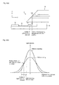
  • the light intensity distribution of signal light rays on the light-receiving face of the optical cable module 1 is formed into one as shown in Fig. 1(b) .
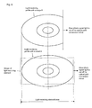
  • the profile (hereinafter, referred to as light-receiving profile) of signal light rays on the light-receiving face of the optical cable module 1 is schematically represented as one shown in Fig. 3 .
  • the light-receiving face in the light-receiving element 11 is formed so as to cover an area that includes this light-receiving profile, the light-receiving face fails to deal with the expanded light-receiving profile in the case when there is a bending in the optical waveguide 10, resulting in a spot-size mismatching loss.
  • the light-receiving profile is subjected to a generation of a comparatively large area to be cut off by the optical path conversion mirror.
  • the light-receiving profile without a bending and the light-receiving profile with a bending are compared with each other, the light-receiving profile with a bending becomes wider; however, even the light-receiving profile with a bending is not expanded toward the side on which the area is cut off by the optical path conversion mirror.
  • the light-receiving face of the light-receiving element is expanded so as to include the light-receiving profile with a bending in the optical waveguide, with the center of the light-receiving element being made coincident with the reflection center of the light axis as in the case of the prior art, the light-receiving element is expanded to the area in which the signal light rays are cut off by the optical path conversion mirror. This causes difficulties in miniaturizing the optical cable module, and also causes a reduction in the response speed of the light-receiving element.
  • the center of the light-receiving element 11 is placed to deviate from the light-axis reflection position toward the end portion side of the optical waveguide 10, that is, toward the side opposite to the side on which the cutting off of the signal light rays is caused by the optical path conversion mirror.
  • the profile of the light-receiving element 11 is reduced so as not to contain the area in which signal light rays are cut off by the optical path conversion mirror, and the light-receiving element 11 is consequently allowed to receive both of the light-receiving profile without a bending in the optical waveguide and the light-receiving profile with a bending in the optical waveguide, without causing any spot-size mismatching loss.
  • the center of the light-receiving element 11 coincident with the center of the light-receiving profile (bending output spot) with a bending, it is possible to obtain the above-mentioned effect by using the minimum light-receiving area.
  • the center of the light-receiving element 11 is not necessarily required to be made completely coincident with the center of the light-receiving profile with a bending.
  • the light-receiving area of the light-receiving element 11 can be set in accordance with the case having the widest light-receiving profile.
  • a shape in which the longitudinal axis is set in the expanding direction of output light rays upon having a bending in the optical waveguide is preferably used, and although not particularly limited, various shapes, such as a rectangular shape, an elliptical shape and a diamond shape, may be used (for example, a light-receiving element having a rectangular shape is shown in Fig. 3 ).
  • FIGs. 4(a) and 4(b) show a modified example of the optical cable module according to the present embodiment 1. Since an optical cable module 2 shown in Fig. 4(a) has a structure similar to that of the optical cable module 1 shown in Fig. 1(a) , those members that are the same as those of the optical cable module 1 are indicated by common reference numbers, and the detailed descriptions thereof will be omitted.
  • the optical cable module 2 shown in Fig. 4(a) differs from the optical cable module 1 shown in Fig. 1(a) in that a light-receiving element 21 is installed therein in place of the light-receiving element 11.
  • the light-receiving element 21 is placed with its center gap from the light-axis reflection position.
  • the following description will discuss the layout of the light-receiving element 21 in detail.
  • Fig. 4(b) shows light intensity distributions of signal light rays on the light-receiving face in both of the states where there is a bending in the optical waveguide 10 and where there is no bending in the optical waveguide 10.
  • the axis of abscissa indicates the distance from the light-axis reflection position and the axis of ordinate indicates the light intensity.
  • the light-receiving element 21 is disposed so that the center of the light-receiving element 21 is virtually made coincident with the position at which the light intensities are made coincident with each other.
  • the quantity of received light by the light-receiving element 21 is made virtually uniform regardless of the presence or absence of a bending in the optical waveguide so that the light-receiving element 21 makes it possible to prevent generation of a spot-size mismatching loss.
  • the quantity of received light can be obtained more uniformly regardless of the presence or absence of a bending.
  • the light-receiving area of the light-receiving element 21 is made too small, the quantity of received signal light is lowered; therefore, the light-receiving area of the light-receiving element 21 is preferably determined by also taking into consideration the quantity of received light to be required.
  • the position at which the light intensities are made coincident and the center of the light-receiving element 21 are not necessarily required to be made completely coincident with each other, and by allowing these to slightly deviate from each other, it sometimes becomes possible to obtain the quantity of received light more uniformly in both of the cases where there is a bending and where there is no bending.
  • An optical cable module 3 shown in Fig. 5(a) is mainly configured by an optical waveguide 30, a light-receiving element 31 and a supporting substrate 34 on its end portion on the light-releasing side.
  • the end portion of the optical waveguide 30 is secured onto the supporting substrate 34 by a bonding process or the like, and the end portion of the optical waveguide 30 and the light-receiving element 31 are secured in their relative positional relationship.
  • the optical cable module 3 may be provided with an electric wire 32 and an electrical connection unit 33 so as to easily take out an electric signal outputted by the light-receiving element 31.
  • the optical waveguide 30 of the optical cable module 3 is configured by a core 30A, an upper clad layer 30B and a lower clad layer 30C.
  • the end face of the optical waveguide 30 is not made perpendicular to the light axis (X-axis), and is diagonally cut off so as to form an optical path conversion mirror 30D.
  • the end face of the optical waveguide 10 is made perpendicular to the XY plane, and inclined so as to make an angle ⁇ ( ⁇ ⁇ 90°) relative to the X-axis.
  • a signal light ray, transmitted through the core 30, is reflected by the optical path conversion mirror 30D, and changed in its proceeding direction to be released toward the light-receiving element 31.
  • the optical waveguide 30 differs from the optical waveguide 10 in that the inclination angle ⁇ of the optical path conversion mirror 30D is set by taking into consideration the quantity of cut-off signal light in the optical path conversion mirror 30D.
  • the optical cable module 3 according to embodiment 2 is characterized in that the inclination angle ⁇ of the optical path conversion mirror 30D is made smaller so that the quantity of signal light to be cut off by the optical path conversion mirror 30D is reduced.
  • the relationship between a light intensity distribution of a signal light ray on a light-receiving face of the light-receiving element 31 and a guided light distribution area taken out by the optical path conversion mirror 30D is given by one shown in Fig. 5(b) . That is, as clearly seen from Fig. 5(b) , in the optical cable module 3, in both of the cases where there is a bending in the optical waveguide 30 and where there is no bending therein, the angle made by the optical path conversion mirror 30D and the light axis of the core 30A can be set so as to allow the light-receiving element 31 to receive almost all the signal light rays transmitted through the optical waveguide 30.
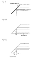
  • Fig. 6 schematically shows a difference in light-receiving profiles due to different inclination angles ⁇ of the optical path conversion mirror.
  • the quantity of signal light to be cut off by the optical path conversion mirror becomes smaller if the inclination angle ⁇ of the optical path conversion mirror is set to a small value. That is, by making the inclination angle ⁇ of the optical path conversion mirror smaller, the optical path conversion loss can be reduced, and consequently, the quantity of received light can be uniformed regardless of the presence or absence of a bending in the optical waveguide.
  • the inclination angle ⁇ of the optical path conversion mirror 30D is preferably set in a range from 37 to 43°.
  • the inclination angle ⁇ of the optical path conversion mirror becomes smaller, the spot size of output light becomes larger, and in an attempt to receive the resulting light, a large light-receiving element is required. As a result, a problem arises in which the communication speed becomes slower. In contrast, as the inclination angle ⁇ of the optical path conversion mirror becomes larger, the area where signal light is cut off by the optical path conversion mirror becomes larger, resulting in a problem of an increase in the optical path conversion loss.
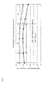
  • Fig. 7 shows the relationship between fluctuations in light-receiving efficiency and a inclination angle ⁇ (mirror angle) of an optical path conversion mirror in both of the states where there is no bending (with a straight line) and where there is a bending (with a bent line) in the optical waveguide.
  • the inclination angle ⁇ of the optical path conversion mirror is preferably set in a range from 37 to 43° from a viewpoint of a permissible range in such a level as not to give adverse effects to a receiving circuit.
  • the light-receiving element 31 may be arranged so that its center is made coincident with the light axis reflection position (assuming that there is light that passes through the center of the cross section of the light axis of the core, a position at which, after having been reflected by the optical path conversion mirror, this light reaches the light-receiving face).
  • the center of the light-receiving element 31 may be placed with a gap from the light axis reflection position, as shown in embodiment 1.
  • Figs. 8(a) and 8(b) show modified example of the optical cable module according to the present embodiment 2. Since the optical cable module 4 shown in Fig. 8(a) has a structure similar to that of the optical cable module 3 shown in Fig. 5(a) , those members that are the same as those of the optical cable module 3 are indicated by common reference numbers, and the detailed descriptions thereof will be omitted.
  • the optical cable module 4 shown in Fig. 8(a) differs from the optical cable module 3 shown in Fig. 5(a) in that an optical waveguide 40 is installed in place of the optical waveguide 30.
  • the optical waveguide 40 is characterized in that, by making the inclination angle ⁇ of the optical path conversion mirror 40D larger, the quantity of signal light to be cut off by the optical path conversion mirror 40D is increased.
  • a relationship between a light intensity distribution of signal light on the light-receiving face of the light-receiving element 31 and a guided light distribution area taken out by the optical path conversion mirror 40D is given by one shown in Fig. 8(b) . That is, as clearly seen from Fig. 8(b) , in the optical cable module 3, in both of cases where there is a bending in the optical waveguide 30 and where there is no bending therein, the angle made by the optical path conversion mirror 40D and the light axis of the core 40A can be set so as to allow the light-receiving element 31 to receive about half the signal light rays transmitted through the optical waveguide 30. This arrangement makes it possible to further miniaturize the light-receiving element, and consequently to make the communication speed faster.
  • Fig. 9 schematically shows light-receiving profiles in both of the states where there is no bending in the optical waveguide 40 and where there is a bending in the optical waveguide 40.
  • the point to which attention should be drawn is that the area where signal light is cut off by the optical path conversion mirror 40D has the light axis reflection position as its border. In this case, regardless of the presence or absence of a bending in the optical waveguide 40, about 1/2 of signal light that has been transmitted through the optical waveguide 40 is cut off by the optical path conversion mirror 40D.
  • the inclination angle ⁇ of the optical path conversion mirror 40D is set so that the border of an area where signal light is cut off by the optical path conversion mirror 40D is made virtually coincident with the light axis reflection position.
  • the inclination angle ⁇ of the optical path conversion mirror 40D is preferably made equal to the critical angle of the optical path conversion mirror 40D.
  • the inclination angle ⁇ of the optical path conversion mirror 40D is desirably set in a range from 50 to 60°.
  • the light-receiving element 31 in the optical cable module 4 is designed so that the center of a light-receiving profile with a bending in the optical waveguide 40 and the center of the light-receiving element 31 are made coincident with each other; thus, it becomes possible to receive signal light rays by using a minimum light-receiving area, without causing any spot-size mismatching loss.
  • the amount of loss of signal light rays in the optical path conversion mirror is controlled.
  • the multilayer reflection film is a film in which two or more kinds of thin films having different refractive indexes are laminated into a multilayer, and by adjusting the thin films to be combined, high-order-mode components can be lost by appropriate amounts so that the light-receiving profiles as shown in Fig. 6 and Fig. 9 can be obtained on demand.
  • a shielding layer reflection layer, absorbing layer or diffusion layer
  • a shielding groove on the bottom portion (on the light-releasing side of the optical path conversion mirror) of the lower clad layer of the optical waveguide, it is possible to desirably control the loss of signal light, and consequently to obtain light-receiving profiles as shown in Figs. 6 and 9 on demand.
  • the optical cable module according to the present embodiments 1 and 2 makes it possible to suppress fluctuations in quantity of signal light due to a shape change of the optical waveguide of the optical cable module. Therefore, the optical cable module can be desirably applied as a flexible wire used for transmitting data through substrates in an apparatus.
  • the optical cable module may be used as a flexible wire in a hinge portion of a portable telephone.
  • the optical cable module of the present invention is of course applicable to many fields, such as notebook personal computers, PDAs, liquid crystal TVs, desktop monitors, printers, electric appliances for automobiles, servers, rooters, testers, and other household apparatuses and general-use apparatuses.
  • the optical cable module of the present invention is provided with a core, a clad layer that surrounds the core around the light axis of the core, an optical waveguide in which an optical path conversion mirror that converts the optical path of signal light by light reflection on its end face is formed on at least one end portion thereof, and a light-receiving element that has a fixed positional relationship relative to the end portion of the optical waveguide, and the center of the light-receiving element is placed with a gap from a first position at which light transmitted through the center of the cross section of the light axis of the core is reflected by the optical path conversion mirror to reach the light-receiving face.
  • the light-receiving face of the light-receiving element is expanded so as to include the light-receiving profile with a bending in the optical waveguide, with the center of the light-receiving element being made coincident with the light-axis reflection center as in the case of conventional devices, the light-receiving element expands up to the area where the signal light is cut off by the optical path conversion mirror. This causes difficulties in miniaturizing the optical cable module, and also causes a reduction in the response speed of the light-receiving element.
  • the center of the light-receiving element is placed with a gap from the first position (light axis reflection position) at which light transmitted through the center of the cross section of the light axis of the core is reflected by the optical path conversion mirror to reach the light-receiving face.
  • the profile of the light-receiving element is reduced as much as possible so as not to contain the area in which signal light is cut off by the optical path conversion mirror, and the light-receiving element is consequently allowed to receive both of the light-receiving profile without bending in the optical waveguide and the light-receiving profile with a bending in the optical waveguide, without causing any spot-size mismatching loss.
  • the light-receiving element is preferably allowed to deviate from the first position in the expanding direction of output light in the case when there is a bending in the optical waveguide.
  • the center of the light-receiving element is preferably arranged so as to be made coincident with the center of a spot of the output light in the case when there is a bending in the optical waveguide.
  • the center of the light-receiving element is preferably placed at a position where the light intensities of the output light with no bending in the optical waveguide and the output light with a bending in the optical waveguide are made virtually equal to each other.
  • the expansion of the signal light is small, with the light intensity in the center being higher.
  • the expansion of the signal light is large, with the light intensity in the center being lower.
  • the light-receiving element is placed so that the center of the light-receiving element is made virtually coincident with the portion where the light intensities are made coincident with each other.
  • another optical cable module is provided with a core, a clad layer that surrounds the core around the light axis of the core, an optical waveguide in which an optical path conversion mirror that converts the optical path of signal light by light reflection on its end face is formed on at least one end portion thereof, and a light-receiving element that has a fixed positional relationship relative to the end portion of the optical waveguide, and the optical path conversion mirror is designed so that the output light from the optical waveguide is made virtually uniform regardless of the presence or absence of a bending in the optical waveguide.
  • the quantity of received light in the light-receiving element can be made uniform.
  • the optical path conversion mirror may be designed so that almost all the signal light transmitted through the optical waveguide can be outputted toward the light-receiving element.
  • the optical path conversion mirror is formed by an end face produced by diagonally cutting off the end portion of the optical waveguide, and the angle made by the optical path conversion mirror and the light axis of the core is preferably set in a range from 37 to 43°.
  • the quantity of received light in the light-receiving element can be uniformed by reducing the optical path conversion loss, as well as by outputting almost all the signal light transmitted through the optical waveguide toward the light-receiving element.
  • the inclination angle of the optical path conversion mirror In order to output almost all the signal light transmitted through the optical waveguide toward the light-receiving element, by setting the inclination angle of the optical path conversion mirror to a small angle, for example, in a range from 37 to 43°, the quantity of signal light to be cut off by the optical path conversion mirror is made smaller so that the optical path conversion loss is reduced.
  • the optical path conversion mirror may be designed so that virtually half of the signal light transmitted through the optical waveguide is outputted toward the light-receiving element.
  • the optical path conversion mirror is formed by an end face produced by diagonally cutting off the end portion of the optical waveguide, and the angle made by the optical path conversion mirror and the light axis of the core is preferably set in a range from 50 to 60°.
  • the quantity of received light in the light-receiving element can be uniformed by outputting virtually half of the signal light transmitted through the optical waveguide toward the light-receiving element.
  • the inclination angle of the optical path conversion mirror In order to output virtually half of the signal light transmitted through the optical waveguide toward the light-receiving element, by setting the inclination angle of the optical path conversion mirror to a large angle, for example, in a range from 50 to 60°, the quantity of signal light to be cut off by the optical path conversion mirror is made larger so that the optical path conversion loss is increased.

Landscapes

  • Physics & Mathematics (AREA)
  • General Physics & Mathematics (AREA)
  • Optics & Photonics (AREA)
  • Engineering & Computer Science (AREA)
  • Microelectronics & Electronic Packaging (AREA)
  • Optical Couplings Of Light Guides (AREA)
  • Optical Integrated Circuits (AREA)

Abstract

An optical cable module is mainly provided with: an optical waveguide (10), a light-receiving element (11) and a supporting substrate (14) at its end portion of the light releasing side. The end portion of the optical waveguide (10) is fixed in its relative positional relationship with the light-receiving element (11). The end face of the optical waveguide (10) is not made perpendicular to the light axis (X-axis), and is diagonally cut so as to form an optical path conversion mirror (10D). Assuming that a light ray (indicated by a solid line in the Figure) that passes through the center of the light-axis cross section of a core (10A), and is reflected by the optical path conversion mirror (10D), and then reaches a light-receiving face at a light axis reflection position, the center of the light-receiving element (11) is placed with a gap from the light axis reflection position, in the optical cable module (1).
Figure imgaf001

Description

    TECHNICAL FIELD
  • The present invention relates to an optical cable module using an optical waveguide, and more particularly to an optical cable module using an optical waveguide having high flexibility.
  • BACKGROUND ART
  • In recent years, an optical communication network capable of executing data communication with a large capacity at high speeds has been expanded. It is expected that, from now on, this optical communication network will be installed not only among apparatuses, but also in apparatuses. Here, in order to achieve a printed circuit board by using optical wiring, an optical waveguide that can be formed into an array has been highly expected.
  • The optical waveguide is formed by a core having a high refractive index and a clad having a low refractive index, which is formed in contact with the periphery of the core so that a light signal that is made incident on the core is transmitted, while being repeatedly total-reflected by the border between the core and the clad.
  • Under these circumstances, recently, there have been strong demands for achieving a flexible optical wiring (in the same manner as in the electric wiring) to be installed in a bendable display and a smaller and thinner household apparatus, by using an optical waveguide. However, since the conventional optical waveguide, which is made from glass or a semiconductor, for example, like an optical coupler to be used for FTTHs, is poor in flexibility, and is not suitable for such applications. That is, film-shaped optical waveguides are demanded.
  • In particular, the inventors, etc. of the present application have developed an optical waveguide having high flexibility, as shown in Fig. 12, by using a further flexible material when compared with the conventional material, as the material for a core and a clad for the optical waveguide. By using this optically guided optical waveguide having high flexibility, even data transfer among substrates in an apparatus can be carried out by using optical waveguides.
  • In the case when this film optical waveguide having flexibility is used as an optical cable, it needs to be properly positioned, and photo-coupled with a photoelectric conversion element (light-receiving/ emitting element). The light-receiving/emitting element is a device that converts an electric signal to a light signal and releases the resulting signal, and also receives a light signal and converts it to an electric signal. Moreover, upon coupling the optical waveguide to the photoelectric conversion element, a structure in which the end portion of the optical waveguide is diagonally cut off to form an optical path conversion mirror on the end face of the optical waveguide has often been used normally. In this optical waveguide having such an optical path conversion mirror, a signal light ray transmitted through the core is converted by the optical path conversion mirror in its proceeding direction, and made incident on a light-receiving element.
    • Patent Document 1: Japanese Patent Application Laid-Open " JP-A No. 2005-78027 (published on March 24, 2005 )"
    • Patent Document 2: Japanese Patent Application Laid-Open " JP-A No. 11-153719 (published on June 8, 1999 )"
    DISCLOSURE OF THE INVENTION
  • In the case when an optical waveguide having high flexibility, as shown in Fig. 12, is used for data transfer among substrates in an apparatus, by making use of its high flexibility, an application for a flexible wiring to be used as portions that are frequently subjected to extending and bending operations (shape changes of the optical waveguide frequently occur), for example, a hinge portion or the like of a portable telephone, has been expected.
  • However, in the optical waveguide, changes in the light wave conditions tend to occur in the optical transfer medium (that is, the core) depending on the bent state of the optical waveguide. Moreover, these changes in the light wave conditions cause a change in the optical path conversion loss and a change in the spot-size mismatching loss. That is, in the conventional optical waveguide, a problem arises in which a large loss difference occurs due to the change in the optical waveguide. The following description will discuss this problem in detail.
  • First, signal light rays to be made incident on the core of an optical waveguide are directed as light rays that are virtually in parallel with the light axis of the core; however, actually, all signal light rays that are in parallel with the light axis of the core are not necessarily made incident thereon. That is, as shown in Fig. 13, signal light rays, transmitted through the optical waveguide, have an angle distribution to a certain degree relative to the light axis of the core. Here, those light rays that are not in parallel with the light axis of the core are transferred inside the core while being reflected by the border face between the core and the clad layer. At this time, if there is no bending in the optical path in the optical waveguide, with a linear optical path being maintained, the angle distribution of the signal light on the light-releasing side is made virtually the same as that on the light-incident side.
  • That is, in the case when there is no bending in the optical waveguide (see Fig. 14(a)), the light intensity distribution of the signal light on the light-receiving face forms one as shown in Fig. 14(b). In the light intensity distribution in this case, the angle distribution of the signal light is small, with the value of the peak quantity of light being large. Here, in Fig. 14, θ represents an angle made by the signal light and the light axis, θc represents a waveguide critical angle (critical angle on the interface between the core and the clad layer), and θc represents a mirror critical angle (critical angle in the optical path conversion mirror).
  • In contrast, as shown in Fig. 15, in the case when there is a bending in the optical path in the optical waveguide, the signal light has a change in its angle relative to the light axis due to reflection at this bent portion. This causes a change in the angle distribution of the signal light on the light-releasing side. More specifically, in the case when there is a bending in the optical waveguide, a signal transmitted through the optical waveguide is expanded in its angle distribution in its bending direction, while being transmitted through this bent portion. Here, the bending direction refers to a direction in parallel with the face including the bent light axis on the cross section perpendicular to the light axis of the optical waveguide.
  • In this manner, while the angle distribution of signal light is changed on the light-releasing side of the optical waveguide, the rate of the signal light to be taken out by the optical path conversion mirror is changed. That is, in the case of the optical path conversion mirror formed by diagonally cutting off the end portion of the optical waveguide, with respect to light rays that are made incident on the cut-off end face with an angle smaller than the critical angle, those light rays that are allowed to transmit the optical path conversion mirror are generated. Here, upon having a change in the angle distribution of the signal light on the light-releasing side, the distribution of incident angle of light onto the optical path conversion mirror is of course changed, resulting in a change in the rate of the signal light to be transmitted through the optical path conversion mirror. More specifically, as the angle distribution of the signal light expands, the rate of the signal light to be transmitted through the optical path conversion mirror increases. That is, the optical path conversion loss in the optical path conversion mirror increases.
  • That is, in the case when the optical waveguide is bent (see Figs. 14(c) and 14(e)), the light intensity distribution of the signal light on the light-receiving face forms one as shown in each of Figs. 14(d) and 14(f). In the light intensity distribution of each of these cases, the angle distribution of the signal light becomes larger, with the value of the peak quantity of light being made smaller. Moreover, since the angle distribution of the signal light becomes larger, the optical path conversion loss of the optical path conversion mirror increases (in Figs. 14(b), 14(d) and 14(f), a hatched portion with slanting lines indicates an optical path conversion loss area in the optical path conversion mirror). Moreover, in the case when the bent portion of the optical waveguide is located close to the output end (see Figs. 14(c) and 14(d)), in addition to the expansion of the angle distribution of the signal light, a gap in the peak position also occurs; however, in the case when the bent portion of the optical waveguide is separated from the output end to a certain degree (see Figs. 14(e) and 14(f)), only the expansion of the angle distribution of the signal light occurs.
  • Moreover, when the angle distribution of the signal light is expanded on the light-releasing side, a releasing-light profile of the released signal light from the optical waveguide to be projected onto the light-receiving face is changed. As a result, a spot-size mismatching loss occurs in the light-receiving element.
  • In this manner, the optical path conversion loss and the spot-size mismatching loss of the signal light due to a shape change of the optical waveguide causes a variation in quantity of signal light to be detected by the light-receiving element. In the case when the variation in quantity of signal light to be detected is large, it is necessary to provide a function for adjusting a gain or the like, so as to expand a dynamic range in the light-receiving unit. As a result, the apparatuses using the above-mentioned optical waveguide tend to have increases in the size, costs and power consumption. This causes great difficulties in utilizing an optical waveguide for data transfer among substrates, in household apparatuses including, for example, portable telephones.
  • The present invention has been devised in view of the above-mentioned problems, and its objective is to achieve an optical cable module that can suppress variations in light quantity of signal light caused by a shape change in an optical waveguide.
  • In order to achieve the above-mentioned objective, an optical cable module according to the present invention is provided with: a core; a clad layer that surrounds the core around the light axis of the core; an optical waveguide in which an optical path conversion mirror that converts the optical path of signal light by light reflection on the end face thereof is formed on at least one end portion thereof; and a light-receiving element that has a fixed positional relationship relative to the end portion of the optical waveguide, and this structure is characterized in that the center of the light-receiving element is placed with a gap from a first position at which light transmitted through the center of the cross section of the light axis of the core is reflected by the optical path conversion mirror to reach the light-receiving face.
  • When there is a bending in the optical waveguide, the angle distribution of signal light that proceeds through the optical waveguide is expanded, with the result that a comparatively large area is generated as an area where the signal light is cut off by the optical path conversion mirror. For this reason, when a light-receiving profile without a bending is compared with a light-receiving profile with a bending, the area becomes larger in the light-receiving profile with the bending; however, even the light-receiving profile with the bending is not expanded toward the side on which the area is cut off by the optical path conversion mirror.
  • For this reason, when the light-receiving face of the light-receiving element is expanded so as to include the light-receiving profile with a bending in the optical waveguide, with the center of the light-receiving element being made coincident with the center of the light axis reflection as in the case of conventional devices, the light-receiving element is expanded to the area where signal light is cut off by the optical path conversion mirror. This causes difficulties in miniaturizing the optical cable module, and also causes a reduction in the response speed of the light-receiving element.
  • In contrast, in accordance with the above-mentioned structure, the center of the light-receiving element is placed with a gap from a first position (light axis reflection position) at which light transmitted through the center of the cross section of the light axis of the core is reflected by the optical path conversion mirror to reach the light-receiving face. With this arrangement, in the light-receiving element, the area where signal light is cut off by the optical path conversion mirror is made as small as possible so as not to be included therein, and both of the light-receiving profile without a bending in the optical waveguide and the light-receiving profile with a bending in the optical waveguide can be received without causing a spot size mismatching loss.
  • Moreover, in order to achieve the above-mentioned objective, another optical cable module according to the present invention is provided with: a core; a clad layer that surrounds the core around the light axis of the core; an optical waveguide in which an optical path conversion mirror that converts the optical path of signal light by light reflection on the end face thereof is formed on at least one end portion thereof; and a light-receiving element that has a fixed positional relationship relative to the end portion of the optical waveguide, and this structure is characterized in that the optical path conversion mirror is formed in such a manner that the output light of the optical waveguide is made virtually uniform regardless of the presence or absence of a bending in the optical waveguide.
  • With this arrangement, since the output light of the optical waveguide is made virtually uniform regardless of the presence or absence of a bending in the optical waveguide, the quantity of received light in the light-receiving element can be made uniform.
  • BRIEF DESCRIPTION OF THE DRAWINGS
    • Figs. 1(a) and 1(b) show an embodiment of the present invention, and Fig. 1 (a) is a cross-sectional view that shows an essential structure of an optical cable module in accordance with embodiment 1. Fig. 1 (b) is a diagram that shows a positional relationship between a light intensity distribution of signal light and a light-receiving element light on a light-receiving face of the optical cable module.
    • Fig. 2(a) is a diagram that shows a reflection state by an optical path conversion mirror in a state where there is no bending in an optical waveguide. Fig. 2(b) is a diagram that shows reflection state by the optical path conversion mirror in a state where there is a bending in the optical waveguide.
    • Fig. 3 is a diagram that schematically shows profiles of signal light rays on the light-receiving face of the optical cable module in both of the states where there is a bending in the optical waveguide and where there is no bending in the optical waveguide.
    • Figs. 4(a) and 4(b) show another embodiment of the present invention, and Fig. 4(a) is a cross-sectional view that shows a modified example of the optical cable module in accordance with embodiment 1. Fig. 4(b) is a diagram that shows light intensity distributions of signal light rays on the light-receiving face in both of the states where there is a bending and where there is no bending in the optical waveguide of the optical cable module.
    • Figs. 5(a) and 5(b) show still another embodiment of the present invention, and Fig. 5(a) is a cross-sectional view that shows an essential structure of an optical cable module in accordance with embodiment 2. Fig. 5(b) is a diagram that shows a relationship between a light intensity distribution of a signal light ray in a waveguide and a guided light distribution area taken out by an optical path conversion mirror, in the optical cable module.
    • Fig. 6 is a diagram that schematically shows a difference between light-receiving profiles caused by different inclination angles of the optical path conversion mirror, in a state where there is a bending in the optical waveguide.
    • Fig. 7 is a graph that shows the relationship between fluctuations in light-receiving efficiency and a inclination angle θ of an optical path conversion mirror in both of the states where there is a bending and where there is no bending in the optical waveguide.
    • Figs. 8(a) and 8(b) show still another embodiment of the present invention, and Fig. 8(a) is a cross-sectional view that shows a modified example of an optical cable module in accordance with embodiment 2. Fig. 8(b) is a diagram that shows a relationship between a light intensity distribution of a signal light ray in a waveguide and a guided light distribution area taken out by an optical path conversion mirror, in the optical cable module.
    • Fig. 9 is a diagram that shows light-receiving profiles in both of the states where there is a bending in the optical waveguide and where there is no bending in the optical waveguide.
    • Fig. 10 is a cross-sectional view that shows a structural example of an optical waveguide in which an optical path conversion mirror is formed as a multilayer reflection film.
    • Fig. 11(a) is a cross-sectional view that shows a structural example of an optical waveguide in which a light-shielding layer is formed on the light-releasing side of the optical path conversion mirror. Fig. 11 (b) is a cross-sectional view that shows a structural example of an optical waveguide in which a light-shielding groove is formed on the light-releasing side of the optical path conversion mirror.
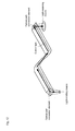
    • Fig. 12 is a perspective view that shows an optical waveguide module.
    • Fig. 13 is a diagram that shows an angle distribution in a signal light ray that is made incident on a core of the optical waveguide.
    • Fig. 14(a) is a side view that shows an optical waveguide in a state where there is no bending. Fig. 14(b) is a diagram that shows a light intensity distribution of a signal light ray on a light-receiving face in the optical waveguide shown in Fig. 14(a). Fig. 14(c) is a side view that shows an optical waveguide in a state where there is a bending close to an output end. Fig. 14(d) is a diagram that shows a light intensity distribution of a signal light ray on a light-receiving face in the optical waveguide shown in Fig. 14(c). Fig. 14(e) is a side view that shows an optical waveguide in a state where there is a bending that is apart from the output end to a certain degree. Fig. 14(f) is a diagram that shows a light intensity distribution of a signal light ray on a light-receiving face in the optical waveguide shown in Fig. 14(e).
    • Fig. 15 is a diagram that shows an angle change in a signal light ray in a state where there is a bending in the optical path of the optical waveguide.
    BEST MODE FOR CARRYING OUT THE INVENTION [Embodiment 1]
  • Referring to drawings, the following description will discuss one embodiment of the present invention. First, referring to Figs. 1(a) and 1(b), one structural example of an optical cable module according to embodiment 1 will be described.
  • An optical cable module 1 shown in Fig. 1(a) is mainly configured by an optical waveguide 10, a light-receiving element 11 and a supporting substrate 14 on its end portion on the light-releasing side. The end portion of the optical waveguide 10 is secured onto the supporting substrate 14 by a bonding process or the like, and the end portion of the optical waveguide 10 and the light-receiving element 11 are secured in the relative positional relationship thereof. Moreover, the optical cable module 1 may be provided with an electric wire 12 and an electrical connection unit 13 so as to easily take out an electric signal outputted by the light-receiving element 11.
  • Here, the end portion of the optical cable module 1 on the reversed side is provided with a light-emitting element in place of the light-receiving element 11 so that a signal incident side end portion is formed. The same structure as that of a conventional optical cable module may be used as the signal incident end portion.
  • First, the optical waveguide 10 is configured by a core 10A, an upper clad layer 10B and a lower clad layer 10C. That is, the optical waveguide 10 has a laminated structure in which the core 10A is sandwiched by the upper clad layer 10B and the lower clad layer 10C. A light signal to be transmitted by the optical waveguide 10 is allowed to proceed the inside of the core 10A, while being reflected by the interface between the core 10A and the upper clad layer 10B or by the interface between the core 10A and the lower clad layer 10C. Here, in Fig. 1(a), in the vicinity of the end portion of the optical waveguide 10, the longitudinal direction (light axis direction) of the optical waveguide 10 is defined as an X-axis direction, and the lamination direction of the core 10A, the upper clad layer 10B and the lower clad layer 10C is defined as a Y-axis direction.
  • The end face of the optical waveguide 10 is not perpendicular to the optical axis (X-axis), and is diagonally cut off to form an optical path conversion mirror 10D. More specifically, the end face of the optical waveguide 10 is made perpendicular to the XY plane, and inclined so as to make an angle θ(θ < 90°) relative to the X-axis. Thus, a signal light ray, transmitted through the core 10, is reflected by the optical path conversion mirror 10D, and changed in its proceeding direction to be released toward the light-receiving element 11. Here, the inclination angle θ of the optical path conversion mirror 10D is normally set to 45° so that the positioning process between the optical path conversion mirror 10D and the light-receiving element 11 is easily carried out. Here, the optical path conversion mirror may be designed so that a mirror unit is externally attached to the end portion of the optical waveguide 10.
  • The point to which attention should be drawn in the optical cable module 1 is the positional relationship between the optical waveguide 10 and the light-receiving element 11. That is, with respect to the positional relationship between the optical waveguide having an optical path conversion mirror and the light-receiving element, conventionally, assuming that there is light (indicated by a solid line in the Figure) that passes through the center of the cross section of the light axis of the core 10A, a position (hereinafter, referred to as a light axis reflection position) at which, after having been reflected by the optical path conversion mirror, this light reaches the light-receiving face is defined as the center position of the light-receiving element. In contrast, the optical cable module 1 according to the present embodiment is characterized in that the center of the light-receiving element 11 is placed so as to deviate from the light axis reflection position.
  • More specifically, in the optical cable module 1, the center of the light-receiving element 11 is allowed to deviate from the light axis reflection position toward the end portion side of the optical waveguide 10. Here, the following description will discuss reasons why the center of the light-receiving element 11 is placed so as to deviate from the light axis reflection position, in detail.
  • First, Fig. 2(a) shows a reflection state by the optical path conversion mirror in a state where there is no bending in the optical waveguide 10, that is, in a state where an angle distribution of a signal light ray transmitted through the optical waveguide 10 is small. Moreover, Fig. 2(b) shows a reflection state by the optical path conversion mirror in a state where there is a bending in the optical waveguide 10, that is, in a state where an angle distribution of a signal light ray transmitted through the optical waveguide 10 is large.
  • In the state where there is no bending in the optical waveguide 10, as shown in Fig. 2(a), almost all the signal light rays that are made incident on the optical path conversion mirror 10D satisfy total reflection conditions of the optical path conversion mirror 10D (that is, made incident on the end face forming the optical path conversion mirror with an angle lower than the critical angle), and converted in its optical path toward the light-receiving side. In contrast, in the state where there is a bending in the optical waveguide 10, as shown in Fig. 2(b), since the angle distribution of signal light rays to be made incident on the optical path conversion mirror 10D expands, with the result that light rays that fail to satisfy the total reflection conditions of the optical path conversion mirror 10D are generated. In other words, in the state where there is a bending in the optical waveguide 10, one portion of the signal light rays to be made incident on the optical path conversion mirror 10D is cut off without being reflected by the optical path conversion mirror.
  • As a result, the light intensity distribution of signal light rays on the light-receiving face of the optical cable module 1 is formed into one as shown in Fig. 1(b). Moreover, the profile (hereinafter, referred to as light-receiving profile) of signal light rays on the light-receiving face of the optical cable module 1 is schematically represented as one shown in Fig. 3. When the light-receiving profile in the case of no bending in the optical waveguide 10 is compared with the light-receiving profile with a bending in the optical waveguide 10, the light-receiving profile with a bending in the optical waveguide 10 becomes wider in a manner so as to correspond to a wider angle distribution of signal light. For this reason, in the case when, assuming that only the light-receiving profile in the case of no bending in the optical waveguide 10 exists, the light-receiving face in the light-receiving element 11 is formed so as to cover an area that includes this light-receiving profile, the light-receiving face fails to deal with the expanded light-receiving profile in the case when there is a bending in the optical waveguide 10, resulting in a spot-size mismatching loss.
  • In contrast, in the case when there is a bending in the optical waveguide 10, the light-receiving profile is subjected to a generation of a comparatively large area to be cut off by the optical path conversion mirror. When the light-receiving profile without a bending and the light-receiving profile with a bending are compared with each other, the light-receiving profile with a bending becomes wider; however, even the light-receiving profile with a bending is not expanded toward the side on which the area is cut off by the optical path conversion mirror.
  • For this reason, when the light-receiving face of the light-receiving element is expanded so as to include the light-receiving profile with a bending in the optical waveguide, with the center of the light-receiving element being made coincident with the reflection center of the light axis as in the case of the prior art, the light-receiving element is expanded to the area in which the signal light rays are cut off by the optical path conversion mirror. This causes difficulties in miniaturizing the optical cable module, and also causes a reduction in the response speed of the light-receiving element.
  • In contrast, in the optical cable module 1 according to the present embodiment 1, the center of the light-receiving element 11 is placed to deviate from the light-axis reflection position toward the end portion side of the optical waveguide 10, that is, toward the side opposite to the side on which the cutting off of the signal light rays is caused by the optical path conversion mirror. With this arrangement, the profile of the light-receiving element 11 is reduced so as not to contain the area in which signal light rays are cut off by the optical path conversion mirror, and the light-receiving element 11 is consequently allowed to receive both of the light-receiving profile without a bending in the optical waveguide and the light-receiving profile with a bending in the optical waveguide, without causing any spot-size mismatching loss.
  • Here, by making the center of the light-receiving element 11 coincident with the center of the light-receiving profile (bending output spot) with a bending, it is possible to obtain the above-mentioned effect by using the minimum light-receiving area. However, the center of the light-receiving element 11 is not necessarily required to be made completely coincident with the center of the light-receiving profile with a bending. Although the above description has simply described the light-receiving profile with a bending, the degree of expansion of the light-receiving profile differs depending on the degree of the bending. For this reason, among the application modes of the optical cable module 1, the light-receiving area of the light-receiving element 11 can be set in accordance with the case having the widest light-receiving profile. Moreover, with respect to the shape of the light-receiving element, a shape in which the longitudinal axis is set in the expanding direction of output light rays upon having a bending in the optical waveguide is preferably used, and although not particularly limited, various shapes, such as a rectangular shape, an elliptical shape and a diamond shape, may be used (for example, a light-receiving element having a rectangular shape is shown in Fig. 3).
  • Next, Figs. 4(a) and 4(b) show a modified example of the optical cable module according to the present embodiment 1. Since an optical cable module 2 shown in Fig. 4(a) has a structure similar to that of the optical cable module 1 shown in Fig. 1(a), those members that are the same as those of the optical cable module 1 are indicated by common reference numbers, and the detailed descriptions thereof will be omitted.
  • The optical cable module 2 shown in Fig. 4(a) differs from the optical cable module 1 shown in Fig. 1(a) in that a light-receiving element 21 is installed therein in place of the light-receiving element 11. The light-receiving element 21 is placed with its center gap from the light-axis reflection position. Here, the following description will discuss the layout of the light-receiving element 21 in detail.
  • First, Fig. 4(b) shows light intensity distributions of signal light rays on the light-receiving face in both of the states where there is a bending in the optical waveguide 10 and where there is no bending in the optical waveguide 10. In Fig. 4(b), the axis of abscissa indicates the distance from the light-axis reflection position and the axis of ordinate indicates the light intensity.
  • As clearly seen from Fig. 4(b), in the light intensity distribution (Gaussian distribution or Lambertian distribution) of signal light with no bending in the optical waveguide 10, the expansion of the signal light is small, with a light intensity in the center portion (peak value) being set to a high level. In contrast, in the light intensity distribution of signal light with a bending in the optical waveguide 10, the expansion of the signal light is large, with a light intensity in the center portion (peak value) being set to a low level.
  • In this case, between the light intensity distribution of signal light with no bending and the light intensity distribution of signal light with a bending, there is a position at which the light intensities are made coincident with each other. In the optical cable module 2, the light-receiving element 21 is disposed so that the center of the light-receiving element 21 is virtually made coincident with the position at which the light intensities are made coincident with each other. Thus, the quantity of received light by the light-receiving element 21 is made virtually uniform regardless of the presence or absence of a bending in the optical waveguide so that the light-receiving element 21 makes it possible to prevent generation of a spot-size mismatching loss.
  • In the light-receiving element 21, as the light-receiving area becomes smaller, the quantity of received light can be obtained more uniformly regardless of the presence or absence of a bending. Here, in the case when the light-receiving area of the light-receiving element 21 is made too small, the quantity of received signal light is lowered; therefore, the light-receiving area of the light-receiving element 21 is preferably determined by also taking into consideration the quantity of received light to be required. Moreover, the position at which the light intensities are made coincident and the center of the light-receiving element 21 are not necessarily required to be made completely coincident with each other, and by allowing these to slightly deviate from each other, it sometimes becomes possible to obtain the quantity of received light more uniformly in both of the cases where there is a bending and where there is no bending.
  • [Embodiment 2]
  • Referring to Drawings, the following description will discuss another embodiment of the present invention. First, referring to Figs. 5(a) and 5(b), one structural example of an optical cable module according to embodiment 2 will be described.
  • An optical cable module 3 shown in Fig. 5(a) is mainly configured by an optical waveguide 30, a light-receiving element 31 and a supporting substrate 34 on its end portion on the light-releasing side. The end portion of the optical waveguide 30 is secured onto the supporting substrate 34 by a bonding process or the like, and the end portion of the optical waveguide 30 and the light-receiving element 31 are secured in their relative positional relationship. Moreover, the optical cable module 3 may be provided with an electric wire 32 and an electrical connection unit 33 so as to easily take out an electric signal outputted by the light-receiving element 31.
  • Here, in the same manner as in the optical waveguide 10 of the optical cable module 1, the optical waveguide 30 of the optical cable module 3 is configured by a core 30A, an upper clad layer 30B and a lower clad layer 30C. Moreover, the end face of the optical waveguide 30 is not made perpendicular to the light axis (X-axis), and is diagonally cut off so as to form an optical path conversion mirror 30D. More specifically, the end face of the optical waveguide 10 is made perpendicular to the XY plane, and inclined so as to make an angle θ (θ < 90°) relative to the X-axis. Thus, a signal light ray, transmitted through the core 30, is reflected by the optical path conversion mirror 30D, and changed in its proceeding direction to be released toward the light-receiving element 31.
  • Here, the optical waveguide 30 differs from the optical waveguide 10 in that the inclination angle θ of the optical path conversion mirror 30D is set by taking into consideration the quantity of cut-off signal light in the optical path conversion mirror 30D.
  • That is, as also described in embodiment 1, when the optical waveguide 30 is bent with the result that the angle distribution of signal light to be made incident on the optical path conversion mirror 30D is expanded, light rays that are made incident on the optical path conversion mirror 30D with a deep angle increase in comparison with the state in which the optical waveguide 30 is not bent. For this reason, the optical cable module 3 according to embodiment 2 is characterized in that the inclination angle θ of the optical path conversion mirror 30D is made smaller so that the quantity of signal light to be cut off by the optical path conversion mirror 30D is reduced.
  • In the optical cable module 3 shown in Fig. 5(a), the relationship between a light intensity distribution of a signal light ray on a light-receiving face of the light-receiving element 31 and a guided light distribution area taken out by the optical path conversion mirror 30D is given by one shown in Fig. 5(b). That is, as clearly seen from Fig. 5(b), in the optical cable module 3, in both of the cases where there is a bending in the optical waveguide 30 and where there is no bending therein, the angle made by the optical path conversion mirror 30D and the light axis of the core 30A can be set so as to allow the light-receiving element 31 to receive almost all the signal light rays transmitted through the optical waveguide 30.
  • In the case when there is a bending in the optical waveguide, Fig. 6 schematically shows a difference in light-receiving profiles due to different inclination angles θ of the optical path conversion mirror.
  • In Fig. 6, in the case when the inclination angle θ of the optical path conversion mirror (for example, θ = 45°) is large, the light-receiving profile has a comparatively large area where the signal light is cut off by the optical path conversion mirror. In contrast, in the case when the inclination angle θ of the optical path conversion mirror (for example, θ = 35°) is small, the light-receiving profile has a smaller area where the signal light is cut off by the optical path conversion mirror.
  • In this manner, even when the angle distribution of signal light is expanded due to a bending occurring in the optical waveguide, the quantity of signal light to be cut off by the optical path conversion mirror becomes smaller if the inclination angle θ of the optical path conversion mirror is set to a small value. That is, by making the inclination angle θ of the optical path conversion mirror smaller, the optical path conversion loss can be reduced, and consequently, the quantity of received light can be uniformed regardless of the presence or absence of a bending in the optical waveguide. Here, in the optical cable module 3, the inclination angle θ of the optical path conversion mirror 30D is preferably set in a range from 37 to 43°.
  • As the inclination angle θ of the optical path conversion mirror becomes smaller, the spot size of output light becomes larger, and in an attempt to receive the resulting light, a large light-receiving element is required. As a result, a problem arises in which the communication speed becomes slower. In contrast, as the inclination angle θ of the optical path conversion mirror becomes larger, the area where signal light is cut off by the optical path conversion mirror becomes larger, resulting in a problem of an increase in the optical path conversion loss.
  • Fig. 7 shows the relationship between fluctuations in light-receiving efficiency and a inclination angle θ (mirror angle) of an optical path conversion mirror in both of the states where there is no bending (with a straight line) and where there is a bending (with a bent line) in the optical waveguide. In an attempt to suppress a difference in fluctuations of the light-receiving efficiency as small as possible between the states where there is no bending in the optical waveguide and where there is a bending therein, the inclination angle θ of the optical path conversion mirror is preferably set in a range from 37 to 43° from a viewpoint of a permissible range in such a level as not to give adverse effects to a receiving circuit.
  • Moreover, in the optical cable module 3, the area where signal light is cut off by the optical path conversion mirror is made smaller. For this reason, the light-receiving element 31 may be arranged so that its center is made coincident with the light axis reflection position (assuming that there is light that passes through the center of the cross section of the light axis of the core, a position at which, after having been reflected by the optical path conversion mirror, this light reaches the light-receiving face). However, even a slight area where signal light is cut off by the optical path conversion mirror is generated, the center of the light-receiving element 31 may be placed with a gap from the light axis reflection position, as shown in embodiment 1.
  • Figs. 8(a) and 8(b) show modified example of the optical cable module according to the present embodiment 2. Since the optical cable module 4 shown in Fig. 8(a) has a structure similar to that of the optical cable module 3 shown in Fig. 5(a), those members that are the same as those of the optical cable module 3 are indicated by common reference numbers, and the detailed descriptions thereof will be omitted.
  • The optical cable module 4 shown in Fig. 8(a) differs from the optical cable module 3 shown in Fig. 5(a) in that an optical waveguide 40 is installed in place of the optical waveguide 30. Here, the optical waveguide 40 is characterized in that, by making the inclination angle θ of the optical path conversion mirror 40D larger, the quantity of signal light to be cut off by the optical path conversion mirror 40D is increased.
  • In the optical cable module 4 shown in Fig. 8(a), a relationship between a light intensity distribution of signal light on the light-receiving face of the light-receiving element 31 and a guided light distribution area taken out by the optical path conversion mirror 40D is given by one shown in Fig. 8(b). That is, as clearly seen from Fig. 8(b), in the optical cable module 3, in both of cases where there is a bending in the optical waveguide 30 and where there is no bending therein, the angle made by the optical path conversion mirror 40D and the light axis of the core 40A can be set so as to allow the light-receiving element 31 to receive about half the signal light rays transmitted through the optical waveguide 30. This arrangement makes it possible to further miniaturize the light-receiving element, and consequently to make the communication speed faster.
  • Here, the following description will discuss in detail reasons why, in the optical waveguide 40, the quantity of signal light to be cut off by the optical path conversion mirror 40D is increased.
  • First, Fig. 9 schematically shows light-receiving profiles in both of the states where there is no bending in the optical waveguide 40 and where there is a bending in the optical waveguide 40. In Fig. 9, the point to which attention should be drawn is that the area where signal light is cut off by the optical path conversion mirror 40D has the light axis reflection position as its border. In this case, regardless of the presence or absence of a bending in the optical waveguide 40, about 1/2 of signal light that has been transmitted through the optical waveguide 40 is cut off by the optical path conversion mirror 40D.
  • That is, in the optical cable module 4, the inclination angle θ of the optical path conversion mirror 40D is set so that the border of an area where signal light is cut off by the optical path conversion mirror 40D is made virtually coincident with the light axis reflection position. With this arrangement, the fluctuations in the quantity of signal light to be cut off by the optical path conversion mirror 40D are eliminated (or reduced) so that the quantity of received light can be uniformed regardless of the presence or absence of a bending in the optical waveguide.
  • In an attempt to allow the border of an area where signal light is cut off by the optical path conversion mirror 40D to be made coincident with the light axis reflection position, the inclination angle θ of the optical path conversion mirror 40D is preferably made equal to the critical angle of the optical path conversion mirror 40D. When the refractive index of a material to be normally used as the optical waveguide is taken into consideration, the inclination angle θ of the optical path conversion mirror 40D is desirably set in a range from 50 to 60°.
  • Moreover, in the same manner as in embodiment 1, the light-receiving element 31 in the optical cable module 4 is designed so that the center of a light-receiving profile with a bending in the optical waveguide 40 and the center of the light-receiving element 31 are made coincident with each other; thus, it becomes possible to receive signal light rays by using a minimum light-receiving area, without causing any spot-size mismatching loss.
  • Moreover, in the optical cable modules 3 and 4 shown in Figs. 5(a) and 8(a), by properly setting the inclination angle θ of the optical path conversion mirror, the amount of loss of signal light rays in the optical path conversion mirror is controlled. However, in addition to this, as shown in Fig. 10, by preparing the optical path conversion mirror of the optical waveguide as a multilayer reflection film, it is possible to also control the amount of loss. The multilayer reflection film is a film in which two or more kinds of thin films having different refractive indexes are laminated into a multilayer, and by adjusting the thin films to be combined, high-order-mode components can be lost by appropriate amounts so that the light-receiving profiles as shown in Fig. 6 and Fig. 9 can be obtained on demand.
  • Moreover, as shown in Figs. 11 (a) and 11 (b), by installing a shielding layer (reflection layer, absorbing layer or diffusion layer) or a shielding groove on the bottom portion (on the light-releasing side of the optical path conversion mirror) of the lower clad layer of the optical waveguide, it is possible to desirably control the loss of signal light, and consequently to obtain light-receiving profiles as shown in Figs. 6 and 9 on demand.
  • As described above, the optical cable module according to the present embodiments 1 and 2 makes it possible to suppress fluctuations in quantity of signal light due to a shape change of the optical waveguide of the optical cable module. Therefore, the optical cable module can be desirably applied as a flexible wire used for transmitting data through substrates in an apparatus. For example, the optical cable module may be used as a flexible wire in a hinge portion of a portable telephone. Not limited to this, the optical cable module of the present invention is of course applicable to many fields, such as notebook personal computers, PDAs, liquid crystal TVs, desktop monitors, printers, electric appliances for automobiles, servers, rooters, testers, and other household apparatuses and general-use apparatuses.
  • As described above, the optical cable module of the present invention is provided with a core, a clad layer that surrounds the core around the light axis of the core, an optical waveguide in which an optical path conversion mirror that converts the optical path of signal light by light reflection on its end face is formed on at least one end portion thereof, and a light-receiving element that has a fixed positional relationship relative to the end portion of the optical waveguide, and the center of the light-receiving element is placed with a gap from a first position at which light transmitted through the center of the cross section of the light axis of the core is reflected by the optical path conversion mirror to reach the light-receiving face.
  • In the case when there is a bending in the optical waveguide, the angle distribution of signal light that proceeds through the optical waveguide is expanded, with the result that an area where the signal light is cut off by the optical path conversion mirror is generated as a comparatively large area. For this reason, when the light-receiving profile without a bending is compared with the light-receiving profile with a bending, the light-receiving profile with a bending becomes larger; however, even the light-receiving profile with a bending is prevented from expanding toward the side with an area having a cut-off portion by the optical path conversion mirror.
  • For this reason, in the case when the light-receiving face of the light-receiving element is expanded so as to include the light-receiving profile with a bending in the optical waveguide, with the center of the light-receiving element being made coincident with the light-axis reflection center as in the case of conventional devices, the light-receiving element expands up to the area where the signal light is cut off by the optical path conversion mirror. This causes difficulties in miniaturizing the optical cable module, and also causes a reduction in the response speed of the light-receiving element.
  • In contrast, in accordance with the above-mentioned arrangement, the center of the light-receiving element is placed with a gap from the first position (light axis reflection position) at which light transmitted through the center of the cross section of the light axis of the core is reflected by the optical path conversion mirror to reach the light-receiving face. With this arrangement, the profile of the light-receiving element is reduced as much as possible so as not to contain the area in which signal light is cut off by the optical path conversion mirror, and the light-receiving element is consequently allowed to receive both of the light-receiving profile without bending in the optical waveguide and the light-receiving profile with a bending in the optical waveguide, without causing any spot-size mismatching loss.
  • Moreover, in the optical cable module, the light-receiving element is preferably allowed to deviate from the first position in the expanding direction of output light in the case when there is a bending in the optical waveguide.
  • Moreover, in the optical cable module, the center of the light-receiving element is preferably arranged so as to be made coincident with the center of a spot of the output light in the case when there is a bending in the optical waveguide.
  • In accordance with the above-mentioned structure, by making the center of the light-receiving element coincident with the center of the receiving light profile in the case when there is a bending in the optical waveguide, it becomes possible to obtain the above-mentioned effects by utilizing the minimum light-receiving area.
  • Moreover, in the optical cable module, the center of the light-receiving element is preferably placed at a position where the light intensities of the output light with no bending in the optical waveguide and the output light with a bending in the optical waveguide are made virtually equal to each other.
  • In the light intensity distribution of signal light with no bending in the optical waveguide, the expansion of the signal light is small, with the light intensity in the center being higher. In contrast, in the light intensity distribution of signal light with a bending in the optical waveguide, the expansion of the signal light is large, with the light intensity in the center being lower.
  • In this case, between the light intensity distribution of signal light with no bending and the light intensity distribution of signal light with a bending, there is a portion where the light intensities are made coincident with each other. In accordance with the above-mentioned structure, the light-receiving element is placed so that the center of the light-receiving element is made virtually coincident with the portion where the light intensities are made coincident with each other. With this arrangement, the quantity of received light by the light-receiving element is made virtually uniform regardless of the presence or absence of a bending in the optical waveguide so that the light-receiving element is allowed to prevent generation of a spot-size mismatching loss.
  • Moreover, another optical cable module according to the present invention is provided with a core, a clad layer that surrounds the core around the light axis of the core, an optical waveguide in which an optical path conversion mirror that converts the optical path of signal light by light reflection on its end face is formed on at least one end portion thereof, and a light-receiving element that has a fixed positional relationship relative to the end portion of the optical waveguide, and the optical path conversion mirror is designed so that the output light from the optical waveguide is made virtually uniform regardless of the presence or absence of a bending in the optical waveguide.
  • In accordance with this structure, since the output light from the optical waveguide is made virtually uniform regardless of the presence or absence of a bending in the optical waveguide, the quantity of received light in the light-receiving element can be made uniform.
  • Moreover, in the optical cable module, the optical path conversion mirror may be designed so that almost all the signal light transmitted through the optical waveguide can be outputted toward the light-receiving element.
  • Furthermore, in the optical cable module, the optical path conversion mirror is formed by an end face produced by diagonally cutting off the end portion of the optical waveguide, and the angle made by the optical path conversion mirror and the light axis of the core is preferably set in a range from 37 to 43°.
  • In accordance with this structure, even when the angle distribution of signal light is expanded by a bending occurred in the optical waveguide, the quantity of received light in the light-receiving element can be uniformed by reducing the optical path conversion loss, as well as by outputting almost all the signal light transmitted through the optical waveguide toward the light-receiving element.
  • In order to output almost all the signal light transmitted through the optical waveguide toward the light-receiving element, by setting the inclination angle of the optical path conversion mirror to a small angle, for example, in a range from 37 to 43°, the quantity of signal light to be cut off by the optical path conversion mirror is made smaller so that the optical path conversion loss is reduced.
  • Moreover, in the optical cable module, the optical path conversion mirror may be designed so that virtually half of the signal light transmitted through the optical waveguide is outputted toward the light-receiving element.
  • Furthermore, in the above-mentioned optical cable module, the optical path conversion mirror is formed by an end face produced by diagonally cutting off the end portion of the optical waveguide, and the angle made by the optical path conversion mirror and the light axis of the core is preferably set in a range from 50 to 60°.
  • In accordance with this structure, even when the angle distribution of signal light is expanded by a bending occurred in the optical waveguide, the quantity of received light in the light-receiving element can be uniformed by outputting virtually half of the signal light transmitted through the optical waveguide toward the light-receiving element.
  • In order to output virtually half of the signal light transmitted through the optical waveguide toward the light-receiving element, by setting the inclination angle of the optical path conversion mirror to a large angle, for example, in a range from 50 to 60°, the quantity of signal light to be cut off by the optical path conversion mirror is made larger so that the optical path conversion loss is increased.
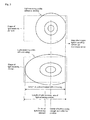
Claims (11)

  1. An optical cable module comprising:
    a core;
    a clad layer that surrounds the core around the light axis of the core;
    an optical waveguide in which an optical path conversion mirror that converts an optical path of signal light by light reflection on the end face thereof is formed on at least one end portion thereof; and
    a light-receiving element that has a fixed positional relationship relative to the end portion of the optical waveguide,
    wherein the center of the light-receiving element is placed with a gap from a first position at which light transmitted through the center of the cross section of the light axis of the core is reflected by the optical path conversion mirror to reach a light-receiving face.
  2. The optical cable module according to claim 1, wherein the light-receiving element is allowed to deviate relative to the first position in an expanding direction of output light when there is a bending in the optical waveguide.
  3. The optical cable module according to claim 1, wherein the center of the light-receiving element is placed so as to be made virtually coincident with a spot center of output light when there is a bending in the optical waveguide.
  4. The optical cable module according to claim 1, wherein the center of the light-receiving element is placed at a position where light intensities of output light when there is no bending in the optical waveguide and output light when there is a bending in the optical waveguide are made virtually equal to each other.
  5. An optical cable module comprising:
    a core;
    a clad layer that surrounds the core around the light axis of the core;
    an optical waveguide in which an optical path conversion mirror that converts an optical path of signal light by light reflection on the end face thereof is formed on at least one end portion thereof; and
    a light-receiving element that has a fixed positional relationship relative to the end portion of the optical waveguide,
    wherein the optical path conversion mirror is formed in such a manner that the optical waveguide has an intensity of output light that is made virtually uniform regardless of the presence or absence of a bending in the optical waveguide.
  6. The optical cable module according to claim 5, wherein an angle made by the optical path conversion mirror and the light axis of the core is set so that the light-receiving element is allowed to receive almost all signal light transmitted through the optical waveguide.
  7. The optical cable module according to claim 1 or 5, wherein the optical path conversion mirror is made of an end face formed by diagonally cutting the end portion of the optical waveguide, with an angle, made by the optical path conversion mirror and the light axis of the core, being set in a range from 37 to 43°.
  8. The optical cable module according to claim 5, wherein an angle made by the optical path conversion mirror and the light axis of the core is set so that the light-receiving element is allowed to receive virtually half of signal light transmitted through the optical waveguide.
  9. The optical cable module according to claim 8, wherein the optical path conversion mirror is made of an end face formed by diagonally cutting the end portion of the optical waveguide, with an angle, made by the optical path conversion mirror and the light axis of the core, being set in a range from 50 to 60°.
  10. The optical cable module according to claim 1 or 5, wherein the light-receiving element has a shape with a longitudinal axis in an expanding direction of output light when there is a bending in the optical waveguide.
  11. An apparatus comprising: the optical cable module according to any of claims 1 to 10.
EP07706615A 2006-01-11 2007-01-11 Optical cable module and apparatus employing it Withdrawn EP1986027A4 (en)

Applications Claiming Priority (2)

Application Number Priority Date Filing Date Title
JP2006004064 2006-01-11
PCT/JP2007/050268 WO2007080932A1 (en) 2006-01-11 2007-01-11 Optical cable module and apparatus employing it

Publications (2)

Publication Number Publication Date
EP1986027A1 true EP1986027A1 (en) 2008-10-29
EP1986027A4 EP1986027A4 (en) 2012-01-04

Family

ID=38256337

Family Applications (1)

Application Number Title Priority Date Filing Date
EP07706615A Withdrawn EP1986027A4 (en) 2006-01-11 2007-01-11 Optical cable module and apparatus employing it

Country Status (6)

Country Link
US (1) US8078022B2 (en)
EP (1) EP1986027A4 (en)
JP (1) JP4905359B2 (en)
KR (1) KR101023337B1 (en)
CN (1) CN101371178B (en)
WO (1) WO2007080932A1 (en)

Cited By (1)

* Cited by examiner, † Cited by third party
Publication number Priority date Publication date Assignee Title
WO2011041204A1 (en) * 2009-09-30 2011-04-07 Corning Incorporated Angle-cleaved optical fibers and methods of making and using same

Families Citing this family (8)

* Cited by examiner, † Cited by third party
Publication number Priority date Publication date Assignee Title
JP2011118306A (en) * 2009-12-07 2011-06-16 Omron Corp Optical transmission module, electronic equipment, method of assembling optical transmission module and optical transmission method
JP5390422B2 (en) * 2010-01-22 2014-01-15 アルプス電気株式会社 Optical element module
US8469610B2 (en) * 2011-01-18 2013-06-25 Avago Technologies General Ip (Singapore) Pte. Ltd. Optical connection system with plug having optical turn
JP2014199229A (en) * 2013-03-29 2014-10-23 住友ベークライト株式会社 Inclination angle measuring method and inclination angle measuring device
JP2016134535A (en) * 2015-01-20 2016-07-25 住友電気工業株式会社 Optical module and manufacturing method of the same
CN107039882B (en) 2014-10-28 2020-07-17 住友电气工业株式会社 Optical modules using light sources, light modulators and input units
JP7215161B2 (en) * 2018-12-27 2023-01-31 住友ベークライト株式会社 Optical waveguide evaluation method and optical module manufacturing method
WO2025204956A1 (en) * 2024-03-28 2025-10-02 日東電工株式会社 Photoelectric conversion module

Family Cites Families (34)

* Cited by examiner, † Cited by third party
Publication number Priority date Publication date Assignee Title
DE2938649A1 (en) * 1978-09-28 1980-04-10 Australian Telecomm DEVICE AND METHOD FOR TRANSMITTING SIGNALS IN LIGHT GUIDES
US4229067A (en) * 1978-11-17 1980-10-21 Corning Glass Works Optical waveguide mode scrambler
DE3563566D1 (en) * 1984-10-09 1988-08-04 Hewlett Packard Co Optical waveguide, particularly optical fiber
JPH02167508A (en) * 1988-09-02 1990-06-27 Fujitsu Ltd Structure of front end of optical fiber
JPH0430581A (en) 1990-05-28 1992-02-03 Fujitsu Ltd Semiconductor light receiving device
JP3100418B2 (en) 1991-05-16 2000-10-16 富士通株式会社 Light receiving device
JP2001507814A (en) * 1996-12-31 2001-06-12 ハネウエル・インコーポレーテッド Flexible optical connector assembly
JPH1123894A (en) * 1997-06-30 1999-01-29 Oki Electric Ind Co Ltd Optical device for optical communication terminal station
JP3064969B2 (en) * 1997-07-03 2000-07-12 日本電気株式会社 Light receiving module and manufacturing method thereof
US5966478A (en) 1997-09-17 1999-10-12 Lucent Technologies Inc. Integrated optical circuit having planar waveguide turning mirrors
JP2000009968A (en) * 1998-06-19 2000-01-14 Matsushita Electric Ind Co Ltd Light receiving module
US6081638A (en) * 1998-07-20 2000-06-27 Honeywell Inc. Fiber optic header with integrated power monitor
JP2000171671A (en) * 1998-12-09 2000-06-23 Matsushita Electric Ind Co Ltd Optical communication module and mounting method thereof
JP2001166186A (en) 1999-09-29 2001-06-22 Matsushita Electric Ind Co Ltd Optical axis adjustment method of optical module, optical module manufacturing method, optical module evaluation method, optical module adjustment / evaluation apparatus, and light receiving element
JP3568156B2 (en) 2000-03-01 2004-09-22 日本電信電話株式会社 Semiconductor device
US20030010904A1 (en) * 2001-07-12 2003-01-16 Luo Xin Simon High speed fiber to photodetector interface
JP2003207694A (en) * 2002-01-15 2003-07-25 Nec Corp Optical module
JP2003294992A (en) 2002-03-29 2003-10-15 Ngk Insulators Ltd Optical device
JP2003295000A (en) * 2002-03-29 2003-10-15 Ngk Insulators Ltd Optical device
US6801687B2 (en) * 2002-08-22 2004-10-05 Terabeam Corporation Apparatus and method for generating a mode-scrambled optical signal using a VCSEL array
DE10307763B4 (en) * 2003-02-14 2005-06-09 Infineon Technologies Ag Electro-optical module for transmitting and / or receiving optical signals of at least two optical data channels
JP2005008027A (en) 2003-06-18 2005-01-13 Kasai Kogyo Co Ltd Opening and closing structure of lid
JP2005078027A (en) 2003-09-03 2005-03-24 Matsushita Electric Ind Co Ltd Optical multiplex transmission system and manufacturing method thereof
JP4340509B2 (en) 2003-10-15 2009-10-07 光錫 徐 Transparent antistatic triacetyl cellulose film for liquid crystal display
JP2005164801A (en) * 2003-12-01 2005-06-23 Nippon Telegr & Teleph Corp <Ntt> Optical waveguide film and method for producing the same
US7184617B2 (en) * 2004-03-12 2007-02-27 Matsushita Electric Industrial Co., Ltd. Portable device
US7496266B2 (en) * 2004-06-25 2009-02-24 Omron Corporation Film waveguide, method of manufacturing film waveguide, and electronic device
EP1770418A4 (en) * 2004-06-28 2010-05-26 Omron Tateisi Electronics Co Optical waveguide, optical waveguide module, optical transmission apparatus, and method for fabricating optical waveguide
JP2006011210A (en) * 2004-06-29 2006-01-12 Fuji Xerox Co Ltd Polymer optical waveguide module with light emitting element and light receiving element for monitoring
JP2007033698A (en) * 2005-07-25 2007-02-08 Fuji Xerox Co Ltd Submount for mounting optical components, and optical transceiver module
US7872664B2 (en) * 2005-09-26 2011-01-18 Ricoh Company, Limited Optical scanning device including shutter member that closes or opens an emission window and image forming apparatus including the optical scanning device
CN101416088B (en) * 2006-04-07 2010-06-16 欧姆龙株式会社 Optical cable module
KR100996805B1 (en) * 2006-04-14 2010-11-25 오므론 가부시키가이샤 Electronic device having an optical transmission module, a connecting part, and an optical transmission module
JP4929821B2 (en) * 2006-04-27 2012-05-09 オムロン株式会社 Optical transmission module

Cited By (2)

* Cited by examiner, † Cited by third party
Publication number Priority date Publication date Assignee Title
WO2011041204A1 (en) * 2009-09-30 2011-04-07 Corning Incorporated Angle-cleaved optical fibers and methods of making and using same
US8477298B2 (en) 2009-09-30 2013-07-02 Corning Incorporated Angle-cleaved optical fibers and methods of making and using same

Also Published As

Publication number Publication date
JPWO2007080932A1 (en) 2009-06-11
EP1986027A4 (en) 2012-01-04
JP4905359B2 (en) 2012-03-28
US8078022B2 (en) 2011-12-13
WO2007080932A1 (en) 2007-07-19
CN101371178B (en) 2010-09-22
KR101023337B1 (en) 2011-03-18
US20100215315A1 (en) 2010-08-26
KR20080072071A (en) 2008-08-05
CN101371178A (en) 2009-02-18

Similar Documents

Publication Publication Date Title
US8078022B2 (en) Optical cable module and apparatus using the same
US7184617B2 (en) Portable device
US7108432B2 (en) Connection structure for optical device, optical device and electronic device
US8588559B2 (en) Optical coupler module having optical waveguide structure
US11822115B2 (en) Display apparatus
EP2733512A2 (en) Optical module and fabrication method
EP3588158B1 (en) Optical-electrical transmission connector and related optical-electrical transmission device
US8805131B2 (en) Optical module and fabrication method
JP2006042307A (en) Portable device
CN101206282B (en) Optical circuit board
US8696216B2 (en) Optical module, method of producing optical module, optical transmission module, and electronic apparatus
US12345932B2 (en) Die last and waveguide last architecture for silicon photonic packaging
CN211148984U (en) Optical transceiver module and optical fiber cable module
US8363988B2 (en) Opto-electronic connector module and opto-electronic communication module having the same
US20100303412A1 (en) Optical transmission module and electronic device
CN101636674B (en) Optical waveguide, optical waveguide module, and electronic apparatus
KR101113416B1 (en) Optical waveguide, optical transmission module, electronic device and method for manufacturing optical waveguide
US20060182442A1 (en) Optical module and electronic device
JP4645651B2 (en) Optical module
KR20080107870A (en) Photoelectric wiring module device and manufacturing method thereof
JP2010192883A (en) Optical and electric combined substrate and method of manufacturing optical and electric combined substrate
US7043107B2 (en) Flexible optical connecting part
CN217587688U (en) Optical device and system for optical module
TWI480608B (en) Optical printed circuit board and method of manufacturing the same
JP2013195444A (en) Image display device module, electronic apparatus, and manufacturing method of image display device module

Legal Events

Date Code Title Description
PUAI Public reference made under article 153(3) epc to a published international application that has entered the european phase

Free format text: ORIGINAL CODE: 0009012

17P Request for examination filed

Effective date: 20080807

AK Designated contracting states

Kind code of ref document: A1

Designated state(s): AT BE BG CH CY CZ DE DK EE ES FI FR GB GR HU IE IS IT LI LT LU LV MC NL PL PT RO SE SI SK TR

A4 Supplementary search report drawn up and despatched

Effective date: 20111205

RIC1 Information provided on ipc code assigned before grant

Ipc: G02B 6/42 20060101AFI20111129BHEP

Ipc: G02B 6/122 20060101ALI20111129BHEP

DAX Request for extension of the european patent (deleted)
STAA Information on the status of an ep patent application or granted ep patent

Free format text: STATUS: THE APPLICATION IS DEEMED TO BE WITHDRAWN

18D Application deemed to be withdrawn

Effective date: 20160802