EP1983811A2 - Electrical Contact - Google Patents
Electrical Contact Download PDFInfo
- Publication number
- EP1983811A2 EP1983811A2 EP08153659A EP08153659A EP1983811A2 EP 1983811 A2 EP1983811 A2 EP 1983811A2 EP 08153659 A EP08153659 A EP 08153659A EP 08153659 A EP08153659 A EP 08153659A EP 1983811 A2 EP1983811 A2 EP 1983811A2
- Authority
- EP
- European Patent Office
- Prior art keywords
- ring portion
- electrical contact
- spring arms
- solder pads
- lie
- Prior art date
- Legal status (The legal status is an assumption and is not a legal conclusion. Google has not performed a legal analysis and makes no representation as to the accuracy of the status listed.)
- Withdrawn
Links
Images



Classifications
-
- H—ELECTRICITY
- H05—ELECTRIC TECHNIQUES NOT OTHERWISE PROVIDED FOR
- H05K—PRINTED CIRCUITS; CASINGS OR CONSTRUCTIONAL DETAILS OF ELECTRIC APPARATUS; MANUFACTURE OF ASSEMBLAGES OF ELECTRICAL COMPONENTS
- H05K3/00—Apparatus or processes for manufacturing printed circuits
- H05K3/40—Forming printed elements for providing electric connections to or between printed circuits
- H05K3/4092—Integral conductive tabs, i.e. conductive parts partly detached from the substrate
-
- H—ELECTRICITY
- H01—ELECTRIC ELEMENTS
- H01R—ELECTRICALLY-CONDUCTIVE CONNECTIONS; STRUCTURAL ASSOCIATIONS OF A PLURALITY OF MUTUALLY-INSULATED ELECTRICAL CONNECTING ELEMENTS; COUPLING DEVICES; CURRENT COLLECTORS
- H01R12/00—Structural associations of a plurality of mutually-insulated electrical connecting elements, specially adapted for printed circuits, e.g. printed circuit boards [PCB], flat or ribbon cables, or like generally planar structures, e.g. terminal strips, terminal blocks; Coupling devices specially adapted for printed circuits, flat or ribbon cables, or like generally planar structures; Terminals specially adapted for contact with, or insertion into, printed circuits, flat or ribbon cables, or like generally planar structures
- H01R12/50—Fixed connections
- H01R12/51—Fixed connections for rigid printed circuits or like structures
- H01R12/55—Fixed connections for rigid printed circuits or like structures characterised by the terminals
- H01R12/57—Fixed connections for rigid printed circuits or like structures characterised by the terminals surface mounting terminals
-
- H—ELECTRICITY
- H01—ELECTRIC ELEMENTS
- H01R—ELECTRICALLY-CONDUCTIVE CONNECTIONS; STRUCTURAL ASSOCIATIONS OF A PLURALITY OF MUTUALLY-INSULATED ELECTRICAL CONNECTING ELEMENTS; COUPLING DEVICES; CURRENT COLLECTORS
- H01R12/00—Structural associations of a plurality of mutually-insulated electrical connecting elements, specially adapted for printed circuits, e.g. printed circuit boards [PCB], flat or ribbon cables, or like generally planar structures, e.g. terminal strips, terminal blocks; Coupling devices specially adapted for printed circuits, flat or ribbon cables, or like generally planar structures; Terminals specially adapted for contact with, or insertion into, printed circuits, flat or ribbon cables, or like generally planar structures
- H01R12/50—Fixed connections
- H01R12/51—Fixed connections for rigid printed circuits or like structures
- H01R12/55—Fixed connections for rigid printed circuits or like structures characterised by the terminals
- H01R12/58—Fixed connections for rigid printed circuits or like structures characterised by the terminals terminals for insertion into holes
-
- H—ELECTRICITY
- H05—ELECTRIC TECHNIQUES NOT OTHERWISE PROVIDED FOR
- H05K—PRINTED CIRCUITS; CASINGS OR CONSTRUCTIONAL DETAILS OF ELECTRIC APPARATUS; MANUFACTURE OF ASSEMBLAGES OF ELECTRICAL COMPONENTS
- H05K3/00—Apparatus or processes for manufacturing printed circuits
- H05K3/30—Assembling printed circuits with electric components, e.g. with resistors
- H05K3/32—Assembling printed circuits with electric components, e.g. with resistors electrically connecting electric components or wires to printed circuits
- H05K3/325—Assembling printed circuits with electric components, e.g. with resistors electrically connecting electric components or wires to printed circuits by abutting or pinching; Mechanical auxiliary parts therefor
- H05K3/326—Assembling printed circuits with electric components, e.g. with resistors electrically connecting electric components or wires to printed circuits by abutting or pinching; Mechanical auxiliary parts therefor the printed circuit having integral resilient or deformable parts, e.g. tabs or parts of flexible circuits
-
- H—ELECTRICITY
- H01—ELECTRIC ELEMENTS
- H01R—ELECTRICALLY-CONDUCTIVE CONNECTIONS; STRUCTURAL ASSOCIATIONS OF A PLURALITY OF MUTUALLY-INSULATED ELECTRICAL CONNECTING ELEMENTS; COUPLING DEVICES; CURRENT COLLECTORS
- H01R13/00—Details of coupling devices of the kinds covered by groups H01R12/70 or H01R24/00 - H01R33/00
- H01R13/02—Contact members
- H01R13/10—Sockets for co-operation with pins or blades
- H01R13/11—Resilient sockets
-
- H—ELECTRICITY
- H01—ELECTRIC ELEMENTS
- H01R—ELECTRICALLY-CONDUCTIVE CONNECTIONS; STRUCTURAL ASSOCIATIONS OF A PLURALITY OF MUTUALLY-INSULATED ELECTRICAL CONNECTING ELEMENTS; COUPLING DEVICES; CURRENT COLLECTORS
- H01R4/00—Electrically-conductive connections between two or more conductive members in direct contact, i.e. touching one another; Means for effecting or maintaining such contact; Electrically-conductive connections having two or more spaced connecting locations for conductors and using contact members penetrating insulation
- H01R4/28—Clamped connections, spring connections
- H01R4/48—Clamped connections, spring connections utilising a spring, clip, or other resilient member
- H01R4/4809—Clamped connections, spring connections utilising a spring, clip, or other resilient member using a leaf spring to bias the conductor toward the busbar
- H01R4/48185—Clamped connections, spring connections utilising a spring, clip, or other resilient member using a leaf spring to bias the conductor toward the busbar adapted for axial insertion of a wire end
- H01R4/4819—Clamped connections, spring connections utilising a spring, clip, or other resilient member using a leaf spring to bias the conductor toward the busbar adapted for axial insertion of a wire end the spring shape allowing insertion of the conductor end when the spring is unbiased
- H01R4/4823—Multiblade spring
-
- H—ELECTRICITY
- H05—ELECTRIC TECHNIQUES NOT OTHERWISE PROVIDED FOR
- H05K—PRINTED CIRCUITS; CASINGS OR CONSTRUCTIONAL DETAILS OF ELECTRIC APPARATUS; MANUFACTURE OF ASSEMBLAGES OF ELECTRICAL COMPONENTS
- H05K2201/00—Indexing scheme relating to printed circuits covered by H05K1/00
- H05K2201/10—Details of components or other objects attached to or integrated in a printed circuit board
- H05K2201/10227—Other objects, e.g. metallic pieces
- H05K2201/1031—Surface mounted metallic connector elements
-
- H—ELECTRICITY
- H05—ELECTRIC TECHNIQUES NOT OTHERWISE PROVIDED FOR
- H05K—PRINTED CIRCUITS; CASINGS OR CONSTRUCTIONAL DETAILS OF ELECTRIC APPARATUS; MANUFACTURE OF ASSEMBLAGES OF ELECTRICAL COMPONENTS
- H05K2201/00—Indexing scheme relating to printed circuits covered by H05K1/00
- H05K2201/10—Details of components or other objects attached to or integrated in a printed circuit board
- H05K2201/10431—Details of mounted components
- H05K2201/1059—Connections made by press-fit insertion
-
- H—ELECTRICITY
- H05—ELECTRIC TECHNIQUES NOT OTHERWISE PROVIDED FOR
- H05K—PRINTED CIRCUITS; CASINGS OR CONSTRUCTIONAL DETAILS OF ELECTRIC APPARATUS; MANUFACTURE OF ASSEMBLAGES OF ELECTRICAL COMPONENTS
- H05K2201/00—Indexing scheme relating to printed circuits covered by H05K1/00
- H05K2201/10—Details of components or other objects attached to or integrated in a printed circuit board
- H05K2201/10613—Details of electrical connections of non-printed components, e.g. special leads
- H05K2201/10954—Other details of electrical connections
- H05K2201/10962—Component not directly connected to the PCB
-
- H—ELECTRICITY
- H05—ELECTRIC TECHNIQUES NOT OTHERWISE PROVIDED FOR
- H05K—PRINTED CIRCUITS; CASINGS OR CONSTRUCTIONAL DETAILS OF ELECTRIC APPARATUS; MANUFACTURE OF ASSEMBLAGES OF ELECTRICAL COMPONENTS
- H05K3/00—Apparatus or processes for manufacturing printed circuits
- H05K3/30—Assembling printed circuits with electric components, e.g. with resistors
- H05K3/306—Assembling printed circuits with electric components, e.g. with resistors with lead-in-hole components
-
- Y—GENERAL TAGGING OF NEW TECHNOLOGICAL DEVELOPMENTS; GENERAL TAGGING OF CROSS-SECTIONAL TECHNOLOGIES SPANNING OVER SEVERAL SECTIONS OF THE IPC; TECHNICAL SUBJECTS COVERED BY FORMER USPC CROSS-REFERENCE ART COLLECTIONS [XRACs] AND DIGESTS
- Y02—TECHNOLOGIES OR APPLICATIONS FOR MITIGATION OR ADAPTATION AGAINST CLIMATE CHANGE
- Y02P—CLIMATE CHANGE MITIGATION TECHNOLOGIES IN THE PRODUCTION OR PROCESSING OF GOODS
- Y02P70/00—Climate change mitigation technologies in the production process for final industrial or consumer products
- Y02P70/50—Manufacturing or production processes characterised by the final manufactured product
Definitions
- the present invention relates to an electrical contact for a circuit board, and in particular to an electrical contact which can be soldered to electric conductors on the circuit board and which has a spring element for mechanical and electrical connection to a terminal pin.
- the aim of the present invention is to provide an improvement to the above-mentioned known arrangements.
- An electrical contact in accordance with the present invention comprises a ring portion defining an opening; a pair of spring arms integral with the ring portion on diametrically opposed sides thereof, and directed inwardly towards one another; and a pair of solder pads spaced from, and integral with, the ring portion on diametrically opposed sides thereof.
- the shape of the ring portion can be more readily adapted to provide improved resilience for the spring arms; improve stress distribution through the contact; and make the contact more susceptible for automated assembly of the contact to a printed circuit board.
- the spring arms lie on a first diametrical axis
- the solder pads lie on a second diametrical axis
- the first and second axes may be substantially perpendicular to one another.
- the first and second axes may be an angle other than ninety degrees. Further still, the first and second axes may be aligned.
- the spring arms are directed inwardly towards one another and at an angle to the plane of the ring portion.
- the spring arms may lie in substantially the same plane as the ring portion.
- the ring portion preferably has a shape which is substantially that of the figure eight.
- the spring arms are preferably formed as the central portion of the eight-shape.
- solder pads are preferably located inside the opening.
- the solder pads are preferably substantially C-shaped and attached to the ring portion by a bridge portion.
- the solder pads may be located outside the ring portion.
- the solder pads lie in a plane which is spaced from the plane of the ring portion.
- the solder pads preferably lie in a plane on the opposite side of the ring portion to the spring arms.
- an electrical contact 10 in accordance with a first embodiment of the present invention includes a ring portion 12 defining an opening 14; a pair of spring arms 16 integral with the ring portion on diametrically opposed sides thereof, and directed inwardly towards one another; and a pair of solder pads 18 spaced from, and integral with, the ring portion on diametrically opposed sides thereof, and positioned within the opening.
- the spring arms 16 lie on a first diametrical axis A 1
- the solder pads 18 lie on a second diametrical axis A 2 , with the first and second axes being substantially perpendicular to one another.
- the ring portion 12 is substantially rectangular with curved corners, and with inwardly curved portions adjacent each spring arm 16 and each solder pad 18.
- the spring arms 16 are directed inwardly towards one another and at an angle to the plane of the ring portion 12.
- the separation of the free ends 20 of the spring arms 12 is a predetermined gap in order to provide a mechanical and electrical connection, by a friction fit, with a corresponding terminal pin (not shown), which may have a circular or rectangular cross-section.
- an electrical contact 110 in accordance with a second embodiment of the present invention includes a ring portion 112 defining an opening 114; a pair of spring arms 116 integral with the ring portion on diametrically opposed sides thereof, and directed inwardly towards one another; and a pair of solder pads 118 integral with, and spaced from, the ring portion on diametrically opposed sides thereof, and positioned within the opening.
- the spring arms 116 lie on a first diametrical axis A 1
- the solder pads 118 lie on a second diametrical axis A 2 , with the first and second axes being substantially perpendicular to one another.
- the ring portion 112 has a shaped which is substantially a figure of eight, with the spring arms 116 being formed from the central part of the eight-shape.
- the spring arms 116 are directed inwardly towards one another and at an angle to the plane of the ring portion 112.
- the separation of the free ends 120 of the spring arms 112 is a predetermined gap in order to provide a mechanical and electrical connection, by a friction fit, with a corresponding terminal pin (referred to below with respect to Figures 3 to 7 ), which may have a circular or rectangular cross-section.
- the solder pads 118 are substantially C-shaped and connected to the ring portion 112 by a bridge portion 122.
- the solder pads 118 preferably lie in a plane which is spaced from the plane of the ring portion 112 on the opposite side to the spring arms 116.
- Figures 3A and B illustrates the use of the electrical contact 110 of Figure 2 .
- the solder pads 118 of the contact 110 are soldered to electrical conductors 124 on a printed circuit board 126.
- the spring arms 116 are located over an aperture 128 in the printed circuit board 126.
- a terminal pin 130 extends through the aperture 128 and makes a mechanical and electrical connection, by a friction grip, with the free ends 120 of the spring arms 116 of the contact.
- Figures 4 and 5 illustrate the use of the contact 110 of Figures 2 and 3 when the terminal pin 130 is integral with a grounding frame 132.
- the printed circuit board has been omitted to illustrate the arrangement.
- the terminal pins 130 have a circular cross-section and engage with a curved portion 134 at the free end 120 of each spring arm 116.
- the terminal pins 130 have a rectangular cross-section and engage with spaced linear portions 136 at the free end 120 of each spring arm 116.
- the connection between the terminal pins 130 and the contacts 110 is as illustrated in Figure 3 .
- the terminal pins 130 and the grounding frame 132 are preferably integrally die-cast.
- Figures 6 and 7 illustrate tolerance compensation which is possible using the contacts of the present invention both in terms of pin dimensions and relative pin position.
- the electrical contact 210 is substantially S-shaped with the ring portion 212 and spring arms 216 defining the central portion of the S-shape and the solder pads 218 defining the outer portions of the S-shape and being positioned outwardly of the ring portion.
- the electrical contact 310 is substantially elongated with the solder pads 318 being positioned outwardly of the ring portion 312 and axially aligned with the spring arms 316.
- the ring portion 212, 312 defines an opening 214, 314 respectively which is substantially rectangular.
- the ring portion 412 of the electrical contact 410 is substantially oval in shape and defines a substantially oval-shaped opening 414.
- the solder pads 418 are positioned outwardly of the ring portion 412 along the longer axis of the oval, and the spring arms 416 lie on an axis substantially perpendicular to the axis of the solder pads.
- Other features of the electrical contacts of Figure 8 to 10 may be as described above with respect to the embodiments shown in Figures 1 and 2 .
- the present invention provides an electrical contact which is readily usable for automated assembly on a printed circuit board along with other circuit board components, thereby avoiding additional selective soldering process at a later stage. Once the contact is soldered then a terminal pin can be pushed into position. At the same time mechanical and electrical connection is provided.
- the present invention has particular application with terminal pins which are die cast integrally with a grounding frame, in which case such terminal pins cannot be readily soldered to electrical contacts.
- the present invention can be applied to different types of printed circuit board and different shapes and types of terminal pin.
- the electrical contact of the present invention has a number of interrelated features.
- the option of positioning of the solder pads surfaces at lower level with the respect to the ring portion assists the automated assembly process. Further, in this respect, mechanical deformation of the contact is possible without interference which allows the ring portion to be spaced from the printed circuit board.
- the shape of the ring portion can provide substantially even distribution of stress and also allows operating in an elastic range once placed on a printed circuit board and mounted together with the terminal pins.
- the spring arms are pre-shaped prior to mounting of the contact on a printed circuit board and further assembly steps. During connection to a terminal pin, the spring arms resiliently deform and make contact with (friction grip) the terminal pin. The elasticity range and friction force can be determined to protect the printed circuit board against disconnection from the terminal pin during normal use. The shape of the free ends of the spring arms can be set to assure the required mechanical and electrical contact between printed circuit board and the terminal pin. The angle of pitch of the spring arms can be optimized to obtain a small assembly force and a high disassembly force.
Landscapes
- Engineering & Computer Science (AREA)
- Manufacturing & Machinery (AREA)
- Microelectronics & Electronic Packaging (AREA)
- Metallurgy (AREA)
- Multi-Conductor Connections (AREA)
- Coupling Device And Connection With Printed Circuit (AREA)
Abstract
Description
- The present invention relates to an electrical contact for a circuit board, and in particular to an electrical contact which can be soldered to electric conductors on the circuit board and which has a spring element for mechanical and electrical connection to a terminal pin.
- It is known to provide an electrical and mechanical connection between a terminal pin and an electrical conductor on a printed circuit board by passing the pin through an aperture in the board, and then soldering the pin to the conductor.
DE 19735409 discloses a known alternative arrangement using an electrical contact. The contact is substantially annular with one or more inwardly directed spring arms. The outer ring portion is soldered to electrical conductors on a printed circuit board. The spring arms overlie an aperture in the circuit board. A terminal pin extends through the aperture, and makes a mechanical and electrical connection with the spring arms by way of a friction grip. - The aim of the present invention is to provide an improvement to the above-mentioned known arrangements.
- An electrical contact in accordance with the present invention comprises a ring portion defining an opening; a pair of spring arms integral with the ring portion on diametrically opposed sides thereof, and directed inwardly towards one another; and a pair of solder pads spaced from, and integral with, the ring portion on diametrically opposed sides thereof.
- By separating the solder area from the ring portion, the shape of the ring portion can be more readily adapted to provide improved resilience for the spring arms; improve stress distribution through the contact; and make the contact more susceptible for automated assembly of the contact to a printed circuit board.
- In a preferred arrangement, the spring arms lie on a first diametrical axis, and the solder pads lie on a second diametrical axis, with the first and second axes being substantially perpendicular to one another. Alternatively, the first and second axes may be an angle other than ninety degrees. Further still, the first and second axes may be aligned.
- Preferably, the spring arms are directed inwardly towards one another and at an angle to the plane of the ring portion. Alternatively, the spring arms may lie in substantially the same plane as the ring portion.
- The ring portion preferably has a shape which is substantially that of the figure eight. In this case, the spring arms are preferably formed as the central portion of the eight-shape.
- The solder pads are preferably located inside the opening. In this case, the solder pads are preferably substantially C-shaped and attached to the ring portion by a bridge portion. Alternatively, the solder pads may be located outside the ring portion.
- Preferably, the solder pads lie in a plane which is spaced from the plane of the ring portion. Where the spring arms are directed away from the plane of the ring portion, the solder pads preferably lie in a plane on the opposite side of the ring portion to the spring arms.
- The present invention will now be described, by way of example, with reference to the accompanying drawings, in which:-
-
Figure 1 is a perspective view of a first embodiment of electrical contact in accordance with the present invention; -
Figure 2 is a perspective view of a second embodiment of electrical contact in accordance with the present invention; -
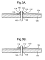
Figure 3A is a cross-sectional view, on axis A1, of the contact ofFigure 2 when soldered to a printed circuit board and attached to a terminal pin; -
Figure 3B is a cross-sectional view, on axis A2, of the contact ofFigure 2 when soldered to a printed circuit board and attached to a terminal pin; -
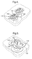
Figure 4 is a perspective view of the contact ofFigure 2 when connected with a round terminal pin; -
Figure 5 is a perspective view of the contact ofFigure 2 when connected with a rectangular terminal pin; -
Figures 6 and 7 illustrate the compensation tolerance of the arrangement shown inFigure 5 ; and -
Figure 8 to 10 are top views of further embodiments of electrical contact in accordance with the present invention. - Referring to
Figure 1 of the drawings, anelectrical contact 10 in accordance with a first embodiment of the present invention includes aring portion 12 defining anopening 14; a pair ofspring arms 16 integral with the ring portion on diametrically opposed sides thereof, and directed inwardly towards one another; and a pair ofsolder pads 18 spaced from, and integral with, the ring portion on diametrically opposed sides thereof, and positioned within the opening. Thespring arms 16 lie on a first diametrical axis A1, and thesolder pads 18 lie on a second diametrical axis A2, with the first and second axes being substantially perpendicular to one another. In this embodiment, thering portion 12 is substantially rectangular with curved corners, and with inwardly curved portions adjacent eachspring arm 16 and eachsolder pad 18. In a preferred arrangement, as shown, thespring arms 16 are directed inwardly towards one another and at an angle to the plane of thering portion 12. The separation of thefree ends 20 of thespring arms 12 is a predetermined gap in order to provide a mechanical and electrical connection, by a friction fit, with a corresponding terminal pin (not shown), which may have a circular or rectangular cross-section. - Referring to
Figure 2 of the drawings, anelectrical contact 110 in accordance with a second embodiment of the present invention includes aring portion 112 defining anopening 114; a pair ofspring arms 116 integral with the ring portion on diametrically opposed sides thereof, and directed inwardly towards one another; and a pair ofsolder pads 118 integral with, and spaced from, the ring portion on diametrically opposed sides thereof, and positioned within the opening. Thespring arms 116 lie on a first diametrical axis A1, and thesolder pads 118 lie on a second diametrical axis A2, with the first and second axes being substantially perpendicular to one another. In this embodiment, thering portion 112 has a shaped which is substantially a figure of eight, with thespring arms 116 being formed from the central part of the eight-shape. In a preferred arrangement, as shown, thespring arms 116 are directed inwardly towards one another and at an angle to the plane of thering portion 112. The separation of thefree ends 120 of thespring arms 112 is a predetermined gap in order to provide a mechanical and electrical connection, by a friction fit, with a corresponding terminal pin (referred to below with respect toFigures 3 to 7 ), which may have a circular or rectangular cross-section. Thesolder pads 118 are substantially C-shaped and connected to thering portion 112 by abridge portion 122. Thesolder pads 118 preferably lie in a plane which is spaced from the plane of thering portion 112 on the opposite side to thespring arms 116. -
Figures 3A and B illustrates the use of theelectrical contact 110 ofFigure 2 . InFigures 3A and B , thesolder pads 118 of thecontact 110 are soldered toelectrical conductors 124 on a printedcircuit board 126. Thespring arms 116 are located over anaperture 128 in the printedcircuit board 126. Aterminal pin 130 extends through theaperture 128 and makes a mechanical and electrical connection, by a friction grip, with thefree ends 120 of thespring arms 116 of the contact. -
Figures 4 and 5 illustrate the use of thecontact 110 ofFigures 2 and3 when theterminal pin 130 is integral with agrounding frame 132. The printed circuit board has been omitted to illustrate the arrangement. InFigure 4 , theterminal pins 130 have a circular cross-section and engage with acurved portion 134 at thefree end 120 of eachspring arm 116. InFigure 5 , theterminal pins 130 have a rectangular cross-section and engage with spacedlinear portions 136 at thefree end 120 of eachspring arm 116. The connection between theterminal pins 130 and thecontacts 110 is as illustrated inFigure 3 . Theterminal pins 130 and thegrounding frame 132 are preferably integrally die-cast.Figures 6 and 7 illustrate tolerance compensation which is possible using the contacts of the present invention both in terms of pin dimensions and relative pin position. - Referring to the further embodiments of electrical contact shown in
Figures 8 to 10 , inFigure 8 theelectrical contact 210 is substantially S-shaped with thering portion 212 andspring arms 216 defining the central portion of the S-shape and thesolder pads 218 defining the outer portions of the S-shape and being positioned outwardly of the ring portion. InFigure 9 , theelectrical contact 310 is substantially elongated with thesolder pads 318 being positioned outwardly of the ring portion 312 and axially aligned with thespring arms 316. InFigures 8 and 9 , thering portion 212, 312 defines anopening Figure 10 , thering portion 412 of theelectrical contact 410 is substantially oval in shape and defines a substantially oval-shaped opening 414. In this embodiment, thesolder pads 418 are positioned outwardly of thering portion 412 along the longer axis of the oval, and thespring arms 416 lie on an axis substantially perpendicular to the axis of the solder pads. Other features of the electrical contacts ofFigure 8 to 10 may be as described above with respect to the embodiments shown inFigures 1 and 2 . - The present invention provides an electrical contact which is readily usable for automated assembly on a printed circuit board along with other circuit board components, thereby avoiding additional selective soldering process at a later stage. Once the contact is soldered then a terminal pin can be pushed into position. At the same time mechanical and electrical connection is provided. The present invention has particular application with terminal pins which are die cast integrally with a grounding frame, in which case such terminal pins cannot be readily soldered to electrical contacts. The present invention can be applied to different types of printed circuit board and different shapes and types of terminal pin.
- The electrical contact of the present invention has a number of interrelated features. The option of positioning of the solder pads surfaces at lower level with the respect to the ring portion (illustrated in
Figure 2 ) assists the automated assembly process. Further, in this respect, mechanical deformation of the contact is possible without interference which allows the ring portion to be spaced from the printed circuit board. The shape of the ring portion can provide substantially even distribution of stress and also allows operating in an elastic range once placed on a printed circuit board and mounted together with the terminal pins. - The spring arms are pre-shaped prior to mounting of the contact on a printed circuit board and further assembly steps. During connection to a terminal pin, the spring arms resiliently deform and make contact with (friction grip) the terminal pin. The elasticity range and friction force can be determined to protect the printed circuit board against disconnection from the terminal pin during normal use. The shape of the free ends of the spring arms can be set to assure the required mechanical and electrical contact between printed circuit board and the terminal pin. The angle of pitch of the spring arms can be optimized to obtain a small assembly force and a high disassembly force.
Claims (14)
- An electrical contact comprising a ring portion defining an opening; and a pair of spring arms integral with the ring portion on diametrically opposed sides thereof, and directed inwardly towards one another; characterised by a pair of solder pads spaced from, and integral with, the ring portion on diametrically opposed sides thereof.
- An electrical contact as claimed in Claim 1, wherein the solder pads are located inside the opening.
- An electrical contact as claimed in Claim 2, wherein the solder pads are substantially C-shaped and attached to the ring portion by a bridge portion.
- An electrical contact as claimed in Claim 1, wherein the solder pads are located outside the ring portion.
- An electrical contact as claimed in any one of the preceding claims, wherein the spring arms lie on a first diametrical axis, and the solder pads lie on a second diametrical axis, with the first and second axes being substantially perpendicular to one another.
- An electrical contact as claimed in any one of Claims 1 to 4, wherein the spring arms lie on a first diametrical axis, and the solder pads lie on a second diametrical axis, with the first and second axes at an angle other than ninety degrees.
- An electrical contact as claimed in any one of Claims 1 to 4, wherein the spring arms lie on a first diametrical axis, and the solder pads lie on a second diametrical axis, with the first and second axes being aligned.
- An electrical contact as claimed in any one of the preceding claims, wherein the spring arms are directed inwardly towards one another and at an angle to the plane of the ring portion.
- An electrical contact as claimed in any one of Claims 1 to 7, wherein the spring arms lie in substantially the same plane as the ring portion.
- An electrical contact as claimed in any one of the preceding claims, wherein the ring portion has a shape which is substantially that of the figure eight.
- An electrical contact as claimed in Claim 10, wherein the spring arms are formed as the central portion of the eight-shape.
- An electrical contact as claimed in any one of the preceding claims, wherein the solder pads lie in a plane which is spaced from the plane of the ring portion.
- An electrical contact as claimed in Claim 12, in which the spring arms are directed away from the plane of the ring portion, wherein the solder pads lie in a plane on the opposite side of the ring portion to the spring arms.
- An electrical contact as claimed in any one of the preceding claims, wherein the contact is substantially S-shaped with the ring portion and spring arms defining the central portion of the S-shape and the solder pads defining the outer portions of the S-shape.
Applications Claiming Priority (2)
| Application Number | Priority Date | Filing Date | Title |
|---|---|---|---|
| DE102007018286A DE102007018286A1 (en) | 2006-05-24 | 2007-04-18 | Electric contact for a circuit board acting as an earth terminal and also to hold the circuit board in the housing |
| GB0719266A GB0719266D0 (en) | 2007-10-03 | 2007-10-03 | electrical contact |
Publications (2)
| Publication Number | Publication Date |
|---|---|
| EP1983811A2 true EP1983811A2 (en) | 2008-10-22 |
| EP1983811A3 EP1983811A3 (en) | 2013-12-11 |
Family
ID=39697227
Family Applications (1)
| Application Number | Title | Priority Date | Filing Date |
|---|---|---|---|
| EP08153659.1A Withdrawn EP1983811A3 (en) | 2007-04-18 | 2008-03-28 | Electrical Contact |
Country Status (1)
| Country | Link |
|---|---|
| EP (1) | EP1983811A3 (en) |
Cited By (7)
| Publication number | Priority date | Publication date | Assignee | Title |
|---|---|---|---|---|
| EP2897230A1 (en) * | 2014-01-21 | 2015-07-22 | Eberspächer catem GmbH & Co. KG | Electrical connection in particular for an electrical heating system of a vehicle |
| WO2018096416A1 (en) * | 2016-11-25 | 2018-05-31 | ローベルト ボッシュ ゲゼルシャフト ミット ベシュレンクテル ハフツング | Brake fluid pressure control device and motorcycle braking system |
| CN112490711A (en) * | 2019-09-12 | 2021-03-12 | 李尔公司 | Electrical connector and electrical connection system |
| JP2021182527A (en) * | 2020-05-20 | 2021-11-25 | 株式会社デンソー | Electronic device |
| US11374366B2 (en) | 2020-06-19 | 2022-06-28 | Lear Corporation | System and method for providing an electrical ground connection for a circuit assembly |
| US11646514B2 (en) | 2020-08-10 | 2023-05-09 | Lear Corporation | Surface mount technology terminal header and method for providing an electrical connection to a printed circuit board |
| US11706867B2 (en) | 2021-01-27 | 2023-07-18 | Lear Corporation | System and method for providing an electrical ground connection for a circuit assembly |
Citations (1)
| Publication number | Priority date | Publication date | Assignee | Title |
|---|---|---|---|---|
| DE19735409A1 (en) | 1997-08-14 | 1999-03-04 | Kathrein Werke Kg | Printed circuit board with contact element |
Family Cites Families (1)
| Publication number | Priority date | Publication date | Assignee | Title |
|---|---|---|---|---|
| DE8901434U1 (en) * | 1989-02-08 | 1990-06-21 | Grote & Hartmann Gmbh & Co Kg, 5600 Wuppertal | Contacting device for a light-emitting diode |
-
2008
- 2008-03-28 EP EP08153659.1A patent/EP1983811A3/en not_active Withdrawn
Patent Citations (1)
| Publication number | Priority date | Publication date | Assignee | Title |
|---|---|---|---|---|
| DE19735409A1 (en) | 1997-08-14 | 1999-03-04 | Kathrein Werke Kg | Printed circuit board with contact element |
Cited By (11)
| Publication number | Priority date | Publication date | Assignee | Title |
|---|---|---|---|---|
| EP2897230A1 (en) * | 2014-01-21 | 2015-07-22 | Eberspächer catem GmbH & Co. KG | Electrical connection in particular for an electrical heating system of a vehicle |
| WO2018096416A1 (en) * | 2016-11-25 | 2018-05-31 | ローベルト ボッシュ ゲゼルシャフト ミット ベシュレンクテル ハフツング | Brake fluid pressure control device and motorcycle braking system |
| JPWO2018096416A1 (en) * | 2016-11-25 | 2019-10-17 | ロベルト・ボッシュ・ゲゼルシャフト・ミト・ベシュレンクテル・ハフツングRobert Bosch Gmbh | Brake fluid pressure control device and motorcycle brake system |
| US20200070791A1 (en) * | 2016-11-25 | 2020-03-05 | Robert Bosch Gmbh | Brake hydraulic pressure controller and motorcycle brake system |
| US10967842B2 (en) | 2016-11-25 | 2021-04-06 | Robert Bosch Gmbh | Brake hydraulic pressure controller and motorcycle brake system |
| CN112490711A (en) * | 2019-09-12 | 2021-03-12 | 李尔公司 | Electrical connector and electrical connection system |
| US20210083413A1 (en) * | 2019-09-12 | 2021-03-18 | Lear Corporation | Electrical connector and electrical connection system |
| JP2021182527A (en) * | 2020-05-20 | 2021-11-25 | 株式会社デンソー | Electronic device |
| US11374366B2 (en) | 2020-06-19 | 2022-06-28 | Lear Corporation | System and method for providing an electrical ground connection for a circuit assembly |
| US11646514B2 (en) | 2020-08-10 | 2023-05-09 | Lear Corporation | Surface mount technology terminal header and method for providing an electrical connection to a printed circuit board |
| US11706867B2 (en) | 2021-01-27 | 2023-07-18 | Lear Corporation | System and method for providing an electrical ground connection for a circuit assembly |
Also Published As
| Publication number | Publication date |
|---|---|
| EP1983811A3 (en) | 2013-12-11 |
Similar Documents
| Publication | Publication Date | Title |
|---|---|---|
| US7249981B2 (en) | Press-fit pin | |
| EP2555334A2 (en) | Connection structure for connecting circuit board, terminal fitting and connection method therefor | |
| US11381012B2 (en) | Electrical connector and electrical connector assembly | |
| JP2016100320A (en) | Connection terminal | |
| CN106663886A (en) | Terminal-equipped printed circuit board | |
| JP6725744B2 (en) | Control unit with press-fit structure | |
| JP7229244B2 (en) | plug connector | |
| US8969734B2 (en) | Terminal assembly with regions of differing solderability | |
| JP2016100215A (en) | Terminal for substrate and substrate with terminal | |
| US4515422A (en) | Pin receptacle intended for mounting in a circuit board | |
| JPS5916398B2 (en) | etsugi card connector | |
| JP2006172986A (en) | Press fit pin | |
| JP2007095629A (en) | Terminal mounting structure and mounting method | |
| KR20010080773A (en) | Device for electrically and mechanically connecting two printed circuit boards | |
| JP2021093345A (en) | Press-fit terminal, substrate with press-fit terminal, and equipment | |
| KR101558743B1 (en) | Connecting pin for electronic circuit board | |
| US12095184B2 (en) | Connector and connector assembly | |
| JP7260314B6 (en) | Press-fit terminals and substrates with terminals | |
| WO2021106546A1 (en) | Press-fit terminal, substrate with press-fit terminal, and device | |
| EP3595416B1 (en) | Control unit having press-fit structure | |
| JP5681261B1 (en) | PCB mounting terminals | |
| JP2001160443A (en) | Terminal and connector equipped with the same | |
| GB2306805A (en) | Conductive rivet electrical termination | |
| JP4001215B2 (en) | Connecting terminal | |
| JP3268253B2 (en) | Socket for electrical components |
Legal Events
| Date | Code | Title | Description |
|---|---|---|---|
| PUAI | Public reference made under article 153(3) epc to a published international application that has entered the european phase |
Free format text: ORIGINAL CODE: 0009012 |
|
| AK | Designated contracting states |
Kind code of ref document: A2 Designated state(s): AT BE BG CH CY CZ DE DK EE ES FI FR GB GR HR HU IE IS IT LI LT LU LV MC MT NL NO PL PT RO SE SI SK TR |
|
| AX | Request for extension of the european patent |
Extension state: AL BA MK RS |
|
| PUAL | Search report despatched |
Free format text: ORIGINAL CODE: 0009013 |
|
| AK | Designated contracting states |
Kind code of ref document: A3 Designated state(s): AT BE BG CH CY CZ DE DK EE ES FI FR GB GR HR HU IE IS IT LI LT LU LV MC MT NL NO PL PT RO SE SI SK TR |
|
| AX | Request for extension of the european patent |
Extension state: AL BA MK RS |
|
| AKY | No designation fees paid | ||
| REG | Reference to a national code |
Ref country code: DE Ref legal event code: R108 |
|
| REG | Reference to a national code |
Ref country code: DE Ref legal event code: R108 Effective date: 20140820 |
|
| STAA | Information on the status of an ep patent application or granted ep patent |
Free format text: STATUS: THE APPLICATION IS DEEMED TO BE WITHDRAWN |
|
| 18D | Application deemed to be withdrawn |
Effective date: 20140612 |