EP1983381A2 - Image forming apparatus - Google Patents
Image forming apparatus Download PDFInfo
- Publication number
- EP1983381A2 EP1983381A2 EP08154795A EP08154795A EP1983381A2 EP 1983381 A2 EP1983381 A2 EP 1983381A2 EP 08154795 A EP08154795 A EP 08154795A EP 08154795 A EP08154795 A EP 08154795A EP 1983381 A2 EP1983381 A2 EP 1983381A2
- Authority
- EP
- European Patent Office
- Prior art keywords
- exposure
- photosensitive drum
- temperature
- potential
- image
- Prior art date
- Legal status (The legal status is an assumption and is not a legal conclusion. Google has not performed a legal analysis and makes no representation as to the accuracy of the status listed.)
- Granted
Links
- 230000008859 change Effects 0.000 claims abstract description 18
- 239000004020 conductor Substances 0.000 claims description 82
- 239000000463 material Substances 0.000 claims description 16
- 238000003860 storage Methods 0.000 claims description 16
- 238000005259 measurement Methods 0.000 claims description 10
- 239000011159 matrix material Substances 0.000 claims description 4
- 125000005843 halogen group Chemical group 0.000 claims description 3
- 125000004435 hydrogen atom Chemical group [H]* 0.000 claims description 3
- XUIMIQQOPSSXEZ-UHFFFAOYSA-N Silicon Chemical group [Si] XUIMIQQOPSSXEZ-UHFFFAOYSA-N 0.000 claims description 2
- 239000013078 crystal Substances 0.000 claims description 2
- 238000012545 processing Methods 0.000 abstract description 35
- 238000012546 transfer Methods 0.000 description 51
- 238000009826 distribution Methods 0.000 description 43
- 238000000034 method Methods 0.000 description 41
- 230000008569 process Effects 0.000 description 33
- 229910021417 amorphous silicon Inorganic materials 0.000 description 32
- 239000010410 layer Substances 0.000 description 26
- 238000012937 correction Methods 0.000 description 19
- 230000007423 decrease Effects 0.000 description 19
- 238000011161 development Methods 0.000 description 17
- 239000010408 film Substances 0.000 description 14
- 230000000875 corresponding effect Effects 0.000 description 12
- 230000003287 optical effect Effects 0.000 description 12
- 230000035945 sensitivity Effects 0.000 description 10
- 238000010586 diagram Methods 0.000 description 7
- 238000004140 cleaning Methods 0.000 description 6
- XAGFODPZIPBFFR-UHFFFAOYSA-N aluminium Chemical compound [Al] XAGFODPZIPBFFR-UHFFFAOYSA-N 0.000 description 5
- 229910052782 aluminium Inorganic materials 0.000 description 5
- 239000003086 colorant Substances 0.000 description 5
- 230000001276 controlling effect Effects 0.000 description 5
- 238000013507 mapping Methods 0.000 description 5
- 230000000873 masking effect Effects 0.000 description 4
- 239000000758 substrate Substances 0.000 description 4
- 238000011144 upstream manufacturing Methods 0.000 description 4
- 230000015572 biosynthetic process Effects 0.000 description 3
- 230000002596 correlated effect Effects 0.000 description 3
- 238000006073 displacement reaction Methods 0.000 description 3
- 230000006870 function Effects 0.000 description 3
- 238000011551 log transformation method Methods 0.000 description 3
- 238000005192 partition Methods 0.000 description 3
- 230000000903 blocking effect Effects 0.000 description 2
- 230000001419 dependent effect Effects 0.000 description 2
- 238000000151 deposition Methods 0.000 description 2
- 230000005684 electric field Effects 0.000 description 2
- 238000002347 injection Methods 0.000 description 2
- 239000007924 injection Substances 0.000 description 2
- 238000003825 pressing Methods 0.000 description 2
- 238000003672 processing method Methods 0.000 description 2
- 230000009467 reduction Effects 0.000 description 2
- 239000004065 semiconductor Substances 0.000 description 2
- 230000003595 spectral effect Effects 0.000 description 2
- 239000002344 surface layer Substances 0.000 description 2
- 230000009466 transformation Effects 0.000 description 2
- 238000004458 analytical method Methods 0.000 description 1
- 238000005513 bias potential Methods 0.000 description 1
- 238000009529 body temperature measurement Methods 0.000 description 1
- 238000004364 calculation method Methods 0.000 description 1
- 239000000969 carrier Substances 0.000 description 1
- 230000015556 catabolic process Effects 0.000 description 1
- 230000005591 charge neutralization Effects 0.000 description 1
- 238000006243 chemical reaction Methods 0.000 description 1
- 238000005229 chemical vapour deposition Methods 0.000 description 1
- 238000004891 communication Methods 0.000 description 1
- 238000004042 decolorization Methods 0.000 description 1
- 230000007547 defect Effects 0.000 description 1
- 238000006731 degradation reaction Methods 0.000 description 1
- 230000001934 delay Effects 0.000 description 1
- 238000001514 detection method Methods 0.000 description 1
- 230000000694 effects Effects 0.000 description 1
- 239000005357 flat glass Substances 0.000 description 1
- 239000007789 gas Substances 0.000 description 1
- 238000009499 grossing Methods 0.000 description 1
- 238000007733 ion plating Methods 0.000 description 1
- 238000004519 manufacturing process Methods 0.000 description 1
- 238000012986 modification Methods 0.000 description 1
- 230000004048 modification Effects 0.000 description 1
- 230000003472 neutralizing effect Effects 0.000 description 1
- 230000006798 recombination Effects 0.000 description 1
- 238000005215 recombination Methods 0.000 description 1
- 230000000284 resting effect Effects 0.000 description 1
- 238000004544 sputter deposition Methods 0.000 description 1
- 230000001629 suppression Effects 0.000 description 1
- 230000001360 synchronised effect Effects 0.000 description 1
- 238000002230 thermal chemical vapour deposition Methods 0.000 description 1
- 239000010409 thin film Substances 0.000 description 1
- 230000001131 transforming effect Effects 0.000 description 1
- 238000013519 translation Methods 0.000 description 1
- 238000001771 vacuum deposition Methods 0.000 description 1
Images







Classifications
-
- G—PHYSICS
- G03—PHOTOGRAPHY; CINEMATOGRAPHY; ANALOGOUS TECHNIQUES USING WAVES OTHER THAN OPTICAL WAVES; ELECTROGRAPHY; HOLOGRAPHY
- G03G—ELECTROGRAPHY; ELECTROPHOTOGRAPHY; MAGNETOGRAPHY
- G03G21/00—Arrangements not provided for by groups G03G13/00 - G03G19/00, e.g. cleaning, elimination of residual charge
- G03G21/20—Humidity or temperature control also ozone evacuation; Internal apparatus environment control
-
- G—PHYSICS
- G03—PHOTOGRAPHY; CINEMATOGRAPHY; ANALOGOUS TECHNIQUES USING WAVES OTHER THAN OPTICAL WAVES; ELECTROGRAPHY; HOLOGRAPHY
- G03G—ELECTROGRAPHY; ELECTROPHOTOGRAPHY; MAGNETOGRAPHY
- G03G15/00—Apparatus for electrographic processes using a charge pattern
- G03G15/50—Machine control of apparatus for electrographic processes using a charge pattern, e.g. regulating differents parts of the machine, multimode copiers, microprocessor control
- G03G15/5033—Machine control of apparatus for electrographic processes using a charge pattern, e.g. regulating differents parts of the machine, multimode copiers, microprocessor control by measuring the photoconductor characteristics, e.g. temperature, or the characteristics of an image on the photoconductor
- G03G15/5045—Detecting the temperature
-
- G—PHYSICS
- G03—PHOTOGRAPHY; CINEMATOGRAPHY; ANALOGOUS TECHNIQUES USING WAVES OTHER THAN OPTICAL WAVES; ELECTROGRAPHY; HOLOGRAPHY
- G03G—ELECTROGRAPHY; ELECTROPHOTOGRAPHY; MAGNETOGRAPHY
- G03G15/00—Apparatus for electrographic processes using a charge pattern
- G03G15/04—Apparatus for electrographic processes using a charge pattern for exposing, i.e. imagewise exposure by optically projecting the original image on a photoconductive recording material
- G03G15/043—Apparatus for electrographic processes using a charge pattern for exposing, i.e. imagewise exposure by optically projecting the original image on a photoconductive recording material with means for controlling illumination or exposure
Definitions
- the present invention relates to an image forming apparatus, such as an electrophotographic copier, laser beam printer, or facsimile machine.
- the transfer member is pressed into contact with or brought in the proximity of a photo conductor, thus forming a transfer portion between the photo conductor and the transfer member.
- a recording material is passed through the transfer portion and a transfer bias voltage that has an opposite polarity to that of a toner image formed on the photo conductor is applied to the transfer member, thereby transferring the toner image on the photo conductor to the surface of the photo conductor.
- Typical examples of the photo conductor for use in the image forming apparatus described above include an organic photo conductor (OPC) and an amorphous silicon photo conductor (hereinafter referred to as an "a-Si photo conductor").
- OPC organic photo conductor
- a-Si photo conductor amorphous silicon photo conductor
- the a-Si photo conductor is used as an electrophotographic photo conductor in, for example, a high-speed copier or laser beam printer because it has a high hardness, exhibits high sensitivity to a semiconductor laser, and also suffers very little degradation caused by repeated use.
- the potential decay (dark decay) occurring after the completion of charging when the a-Si photo conductor is used is larger than that occurring when the organic photo conductor is used. It is well known that the potential decay characteristics of the photo conductor have temperature dependence. Therefore, it is well known that an exposure dose varied in consideration of change in potential decay characteristics dependent on the overall temperature of the image forming apparatus can be employed.
- an image forming apparatus according to one of claims 1 to 7.
- An embodiment of the present invention is capable of forming an excellent image whose image-density irregularities are suppressed even when unevenness in temperature is present inside the image forming apparatus.
- Fig. 1 is a schematic sectional view that illustrates a structure of an image forming apparatus according to an embodiment of the present invention.
- Figs. 2A to 2F are schematic sectional views for describing a layered structure of a photo conductor.
- Fig. 3 is a schematic perspective view of an example of a photosensitive drum and its surroundings.
- Fig. 4A is a vertical sectional view that illustrates a state in which a contact of the resting photosensitive drum is connected to a pin of a main body of the image forming apparatus
- Fig. 4B is a vertical sectional view that illustrates a state in which the pin is detached from the contact and the photosensitive drum is rotatable.
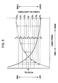
- Fig. 5 is a graph of a relation between an exposure condition of the photo conductor and a potential (EV curve).
- Fig. 6 is a flowchart of an image output process.
- Fig. 7 is a graph that shows an example of potential distribution in a surface of the photosensitive drum after the surface is exposed.
- Fig. 8 is a schematic diagram of potentials of a plurality of regions of the surface of the photosensitive drum after the surface is exposed.
- Fig. 9 is a block diagram for describing an example of image processing.
- Fig. 10 is a block diagram of a process for correcting an exposure condition.
- Fig. 11 is a flowchart of a process for correcting a potential decay characteristic table according to a second embodiment.
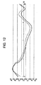
- Fig. 12 is a graph that shows an example of distribution of the surface potential of the photosensitive drum after the surface is exposed.
- Fig. 13 is a schematic diagram of potentials of a plurality of regions of the surface of the photosensitive drum after the surface is exposed.
- Fig. 14 is a schematic perspective view of the photosensitive drum and its surroundings according to a fourth embodiment.
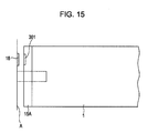
- Fig. 15 is a sectional view that illustrates the photosensitive drum including a tag memory and an antenna substrate of the main body of the image forming apparatus.
- Fig. 16 is a graph that shows an example of temperature distribution in the vicinity of the surface of the photosensitive drum.
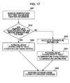
- Fig. 17 is a flowchart of a process for controlling an exposure condition according to the first embodiment.
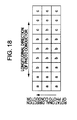
- Fig. 18 is a schematic diagram of temperature characteristics of a plurality of regions of the surface of the photosensitive drum according to a third embodiment.
- Fig. 1 is a schematic vertical sectional view that illustrates a structure of an image forming apparatus according to an embodiment of the present invention.
- An image forming apparatus 100 of the present embodiment is a laser beam printer that employs the tandem system and the intermediate transfer process and can form a full-color image.
- the image forming apparatus 100 includes first, second, third, and fourth image forming portions 10a, 10b, 10c, and 10d as a plurality of image forming units inside a main body A of the image forming apparatus (hereinafter, the main body of the image forming apparatus is referred to as a "main body of the apparatus").
- the first, second, third, and fourth image forming portions 10a, 10b, 10c, and 10d form yellow, magenta, cyan, and black images, respectively.
- structures and operations of the first to fourth image forming portions 10a to 10d are substantially the same, except that the image forming portions use different toner colors.
- the image forming portion 10 includes a drum-type electrophotographic photo conductor (hereinafter referred to as a "photosensitive drum") 1 as an image bearing member.
- the photosensitive drum 1 is rotated in the direction of the arrow R1 in the drawing.
- a charging device 2 as a charging unit and an exposure device 3 (laser scanner) 3 as an exposure unit (exposure system) are disposed around the photosensitive drum 1.
- a developing device 4 as a developing unit and a cleaning device (cleaner) 6 as a cleaning unit are disposed around the photosensitive drum 1.
- a transfer device 5 is disposed so as to face the photosensitive drums 1a to 1d of the image forming portions 10a to 10d.
- a potential sensor 11 as a detecting unit configured to detect the potential of the surface of the photosensitive drum 1 and a temperature sensor 12 as a temperature measuring device configured to measure temperature of adjacent areas of the surface of the photosensitive drum 1 are disposed around the photosensitive drum 1.
- a pre-exposure device (pre-exposure light source) 13 as a charge neutralizing unit configured to remove charges on the photosensitive drum 1 is disposed around the photosensitive drum 1.
- the transfer device 5 includes an endless intermediate transfer belt 51 as an intermediate transfer member.
- the intermediate transfer belt 51 is wound around rollers as a supporting member and is moved around them (rotated) in the direction of the arrow R2 in the drawing.
- Primary transfer rollers 52a to 52d as a primary transfer portion are disposed inside the intermediate transfer belt 51 so as to face the photosensitive drums 1a to 1d, respectively.
- the primary roller 52 presses the intermediate transfer belt 51 against the photosensitive drum 1 and forms a nip portion (primary transfer nip) at a primary transfer portion N1 where the photosensitive drum 1 and the intermediate transfer belt 51 are in contact with each other.
- a secondary transfer roller 53 constituting a secondary transfer portion and a conveying belt 54 are disposed outside the intermediate transfer belt 51 so as to face one roller (secondary transfer opposite roller) 55 of rollers around which the intermediate transfer belt 51 is wound.
- the secondary transfer roller 53 is disposed inside the conveying belt 54 and is in contact with the secondary transfer opposite roller 55 via the conveying belt 54 and the intermediate transfer belt 51 arranged therebetween. This forms a nip portion (secondary transfer nip) at a secondary transfer portion N2 being a contact portion between the intermediate transfer belt 51 and the conveying belt 54.
- a charge position charged by the charging device 2, an exposure position exposed by the exposure device 3, a development position developed by the developing device 4, a primary transfer position primarily transferred by the primary transfer roller 52, and a cleaning position cleaned by the cleaning device 6 on the photosensitive drum 1 are arranged in this order along the rotational direction of the photosensitive drum 1.
- a potential detection position detected by the potential sensor 11 on the photosensitive drum 1 is arranged downstream of the exposure position and upstream of the development position in the rotational direction of the photosensitive drum 1.
- a circumferential temperature measurement position measured by the temperature sensor 12 on the photosensitive drum 1 is arranged downstream of the development position and upstream of the primary transfer position in the rotational direction of the photosensitive drum 1.
- a charge neutralization position performed by the pre-exposure device 13 on the photosensitive drum 1 is arranged downstream of the cleaning position and upstream of the charge position in the rotational direction of the photosensitive drum 1.
- a conveying device 7 as a recording-material supplying unit, a fixing device 8 as a fixing unit, and a recording-material output tray T as a recording-material eject unit are arranged inside the main body A of the apparatus in this order from the upstream along the direction of conveyance of a recoding material (for example, paper) P.
- an image reading device (original plate scanner) 9 as an image reading unit is disposed above the main body A of the apparatus.
- the photosensitive drum 1 is one in which a-Si photo conductor layers are laminated on the periphery of an aluminum cylinder.
- the photosensitive drum 1 is rotated by a driving unit (not shown) in the direction of the arrow R1 in the drawing at a predetermined process speed.
- the photosensitive drum 1 will be described in greater detail below.
- the surface of the photosensitive drum 1 is uniformly charged by the charging device 2 to have a predetermined polarity and a predetermined potential.
- One example of the charging device 2 is a corona charger that is in non-contact with the photosensitive drum 1.
- the charged photosensitive drum 1 is scanned and exposed by the exposure device 3, and an electrostatic (latent) image is thereby formed on the surface of the photosensitive drum 1.
- the image reading device 9 includes a light source 92 movable in the direction of the arrow m and in a direction opposite thereto.
- the light source 92 irradiates an image surface of a document placed on an original plate glass 91, the image surface facing down.
- Light reflected from the image surface is read by a charge-coupled device (CCD) (full-color sensor) 94 being an image pickup element (photoelectric conversion element) via a reflector 95 and a lens 93.
- CCD charge-coupled device
- full-color sensor full-color sensor
- the exposure device 3 exposes the surface of the photosensitive drum 1 in accordance with the image information input from the image reading device 9 and forms an electrostatic latent image thereon.
- the exposure device 3 includes a laser oscillator 31, a polygonal mirror 32, a lens 33, and a reflector 34.
- Toner is attached to the electrostatic latent image formed on the surface of the photosensitive drum 1 by the developing device 4, and the electrostatic latent image is developed as a toner image.
- the toner image formed on the photosensitive drum 1 is transferred (primarily) to the intermediate transfer belt 51 by the primary transfer roller 52.
- a voltage (primary transfer bias) having a polarity opposite to a normal charge polarity of toner is applied to the primary transfer roller 52.
- full-color image forming for example, the charging, exposing, and primarily transferring processes described above are performed in the first to fourth image forming portions 10a to 10d.
- toner images of different colors are sequentially overlaid and are primarily transferred onto the intermediate transfer belt 51.
- superimposed images are formed on the intermediate transfer belt 51.
- the recording material P accommodated in a recording-material cassette 71 of the conveying device 7 is transported by a recording-material supply roller 72 and is supported on the surface of the conveying belt 54 wound around a plurality of rollers by a conveying roller and other elements.
- the toner images formed on the intermediate transfer belt 51 are collectively transferred (secondarily) to the surface of the recording material P supported on the conveying belt 54.
- a voltage (secondary transfer bias) having a polarity opposite to a normal charge polarity of toner is applied to the secondary transfer roller 53.
- the recording material P with the combined toner image transferred is conveyed to the fixing device 8 by the conveying belt 54.
- the toner image is heated and pressed by a fixing roller 81 and a pressing roller 82, and the toner image is fixed on the surface. Subsequently, the recording material P is ejected onto the recording-material output tray T.
- Toner remaining on the photosensitive drum 1 after the completion of a primary transfer process is removed and collected by the cleaning device 6.
- Toner remaining on the intermediate transfer belt 51 after the completion of a secondary transfer process is removed and collected by an intermediate transfer member cleaner (not shown).
- the image forming apparatus 100 can also form a monochrome image using only the fourth image forming portion 10d, for example.
- an image forming operation is the same as that described above, except that there are image forming portions that do not perform image formation.
- FIG. 2A to 2F is a schematic diagram that illustrates a part of portions located above an axis of the photosensitive drum 1 in a vertical sectional view that includes the axis.
- the photoconductive layer is formed from a non-single-crystal material that contains silicon atoms as a matrix and at least one of hydrogen atoms and halogen atoms (hereinafter, this material is referred to as an a-Si: H, X (H represents a hydrogen atom and X represents a halogen atom)).
- the photosensitive drum 1 shown in Fig. 2A includes a cylindrical conductive drum (support) 21 and a photosensitive layer 22 formed on the surface of the conductive drum 21.
- the conductive drum 21 is composed of, for example, aluminum as a photo conductor.
- the photosensitive layer 22 includes a photoconductive layer 23 composed of a-Si: H, X.
- the photosensitive drum 1 shown in Fig. 2B includes a conductive drum 21 and a photosensitive layer 22 formed on the surface of the conductive drum 21.
- the conductive drum 21 is composed of, for example, aluminum as a photo conductor.
- the photosensitive layer 22 includes a photoconductive layer 23 composed of a-Si: H, X and an amorphous silicon based surface layer 24.
- the photosensitive layer 22 may further include an amorphous silicon based charge injection blocking layer 25.
- the photoconductive layer 23 may include a charge generation layer 27 and a charge transport layer 28 that are composed of a-Si: H, X.
- the amorphous silicon based surface layer 24 may be included in the photoconductive layer 23.
- the charge injection blocking layer 25 is disposed as needed to block charges from being injected from the conductive drum 21 to the photoconductive layer 23.
- the conductive drum 21 may be conductive in itself, or alternatively, be electrically insulative one that is electrically conductive treated.
- the photoconductive layer 23 being a part of the photosensitive layer 22 overlies the conductive drum 21 or, as required, an underlayer (not shown).
- the photoconductive layer 23 can be formed by well-known techniques for depositing thin films, such as plasma (enhanced) chemical vapor deposition (p-CVD), sputtering, vacuum deposition, ion plating, photo CVD, and thermal CVD.
- p-CVD plasma chemical vapor deposition
- the p-CVD process can use frequency bands of an RF band, VHF band, and UHF band.
- Each of the layers described above can be made by well-known apparatuses and film formation techniques.
- the thickness of the photoconductive layer 23 is appropriately determined in consideration of that desired electrophotographic characteristics are obtainable, capacitance in use can be within a desired range, and economic effects are achievable.
- the thickness of the photoconductive layer 23 can be 20 ⁇ m to 50 ⁇ m.
- reference numeral 26 represents a free surface.
- uneven temperature distribution may occur inside a machine by unbalanced arrangement of heat sources, such as the fixing device 8 and motor, and airflow.
- the present embodiment can form an excellent image whose image-density irregularities are suppressed even when unevenness in temperature is present inside the image forming apparatus.
- the present embodiment can omit or simplify a temperature control device, such as a heater, to maintain the temperature of the photo conductor constant.
- the exposure conditions for exposure performed by the exposure device 3 are changed by an image processing circuit 200.
- the exposure conditions are changed by modulating the pulse width of a signal to be input to the exposure device.
- a great pulse width corresponds to a large amount of exposure dose per unit area
- a narrow pulse width corresponds to a small amount of exposure dose per unit area.
- Another way of changing the exposure conditions is to change the exposure dose per unit area by increasing laser power by modulating the intensity of the exposure.
- two or more temperature measuring devices are disposed inside the main body A of the apparatus, and the exposure conditions are corrected based on the temperature distribution inside the main body A of the apparatus.
- the image forming apparatus 100 includes the photosensitive drum 1, which is an image bearing member that has a movable surface having a photoconductive layer, and the charging device 2, which charges the surface of the photosensitive drum 1.
- a corona charger is used as the charging device 2.
- the image forming apparatus 100 includes the exposure device 3 as an exposure unit configured to expose the charged surface of the photosensitive drum 1 and to form an electrostatic latent image thereon and the image processing circuit 200 as a control unit configured to control the exposure performed by the exposure device 3 in accordance with image information.
- the image processing circuit 200 as the control device generates exposure data based on the image information.
- the image forming apparatus 100 includes the developing device 4 as a developing unit configured to attach toner to the electrostatic latent image and to develop it as a toner image and a transferring unit configured to transfer the toner image from the photosensitive drum 1 to another member.
- the image forming apparatus 100 includes a memory chip 300 ( Figs. 4A and 4B ) as a storage unit that stores a temperature characteristic of the surface potential of the photosensitive drum 1.
- the temperature characteristic of the surface potential is typically the amount of change in the surface potential per unit temperature.
- the longitudinal direction of the photosensitive drum 1 is typically a direction transverse to (substantially perpendicular to) the direction of movement of the surface of the photosensitive drum 1 (rotational direction thereof) and is typically a main scanning direction in optical scanning of the exposure device 3.
- the exposure conditions during exposure of the exposure device 3 can be changed in accordance with the temperature characteristic stored in the memory chip 300.
- the exposure potential potential of the photosensitive drum at the exposure position after exposure
- the memory chip 300 has a control table that controls the exposure conditions such that the exposure potential is increased by approximately 2-3 V for every 1°C rise in temperature of the photo conductor.
- the image forming apparatus 100 includes the temperature sensor 12 as a temperature measuring device capable of measuring temperatures in two different locations in the longitudinal direction of the photosensitive drum 1 to measure temperature inside the main body A of the apparatus correlated with the surface temperature of the photosensitive drum 1. In the present embodiment, two temperature sensors 12A and 12B are included as the temperature sensor 12.
- the image processing circuit 200 changes the exposure conditions for exposure performed by the exposure device 3 based on measured values measured by these two temperature sensors 12 and the potential decay characteristic table. The details will be described below.
- the exposure conditions are corrected based on temperature distribution inside (within the machine of) the main body A of the apparatus.
- the plurality of temperature sensors 12 as a temperature measuring device are arranged in different locations in the longitudinal direction of the photosensitive drum 1 to measure temperatures of adjacent areas of the surface of the photosensitive drum 1.
- the two temperature sensors are arranged such that the first temperature sensor 12A is disposed adjacent to an end of the photosensitive drum 1 corresponding to the rear side of the main body A (the end is the leading end when the photosensitive drum 1 is mounted in the main body A of the apparatus) and the second temperature sensor 12B is disposed adjacent to the other front-side end.
- thermocouple or, for example, thermistors capable of measuring the temperature of an atmosphere near the surface of the photosensitive drum 1 is used.
- the length of the photosensitive drum 1 in the longitudinal direction is approximately 380 mm, whereas the first temperature sensor 12A is located approximately 30 mm away from the rear end of the photosensitive drum 1 and the second temperature sensor 12B is located approximately 30 mm away from the front end of the photosensitive drum 1.
- the distance between the photosensitive drum 1 and each of the first and second temperature sensors 12A and 12B is approximately 5 mm.
- the arrangement of the temperature sensors 12 is not limited to the above.
- the temperature sensors 12 can have any structure and be placed in any location as long as they can measure temperature variations of the main body of the image forming apparatus, the temperature variations affecting the potential decay characteristics of the photosensitive drum 1, with a desired accuracy.
- the temperature sensors 12 can have a structure and be arranged so as to measure temperature of the inside of the main body A of the apparatus, the temperature being correlated with the surface temperature of the photosensitive drum 1 affecting the potential decay characteristics of the photosensitive drum 1.
- the temperature sensors 12 may be arranged in a location slightly displaced from the photosensitive drum 1, instead of being arranged immediately above the photosensitive drum 1.
- the temperature of adjacent area of the surface of the photosensitive drum 1 for example, the temperature of a region 5 mm to 20 mm away from the surface of the photosensitive drum 1 can be measured. Moreover, the temperature of a region 10 mm or less away from the surface of the photosensitive drum 1 can be measured.
- the temperature of the surface of the photosensitive drum 1 can also be measured in a non-contact manner using an infrared temperature measuring device or other devices. If the surface of the photosensitive drum 1 can be measured without damage to the photosensitive drum 1, directly measuring the surface temperature leads to more accurate control. In this case, a non-contact temperature measuring device, as described above, can be used.
- Fig. 16 shows one example of an arrangement of the first and second temperature sensors 12A and 12B and temperature distribution in adjacent areas of the surface of the photosensitive drum 1. The state in Fig. 16 is that the temperature adjacent to the first temperature sensor 12A is higher than the temperature adjacent to the second temperature sensor 12B.
- the potential of a region adjacent to the first temperature sensor 12A tends to decrease, whereas the potential of a region adjacent to the second temperature sensor 12B is less prone to decrease.
- the exposure dose is reduced to a value at which the exposure potential of the photosensitive drum 1 is increased by 3 V when exposure is performed at the reference temperature.
- FIG. 17 A flowchart of a process for controlling the exposure conditions in consideration of unevenness in temperature is shown in Fig. 17 .
- step S301 the image processing circuit 200 reads results of measurement performed by the first and second temperature sensors 12A and 12B. Then, in step S302, the image processing circuit 200 determines whether the temperatures measured by the first and second temperature sensors 12A and 12B are the same.
- step S303 temperature distribution inside the main body A of the apparatus, more specifically, temperature distribution in adjacent areas of the surface of the photosensitive drum 1 in the longitudinal direction of the photosensitive drum 1 is calculated.
- step S304 the image processing circuit 200 corrects the exposure conditions in the longitudinal direction of the photosensitive drum 1 based on temperature characteristics of the surface potential of the photosensitive drum 1 and the calculated temperature distribution inside the main body A of the apparatus.
- step S305 exposure is performed based on image information and the exposure conditions corrected using the temperature sensors.
- step S302 When the image processing circuit 200 determines that the temperatures measured by the first and second temperature sensors 12A and 12B are the same (YES in step S302), the following process is performed. That is, in this case, it is determined that temperature distribution inside the main body A of the apparatus, more specifically, temperature distribution in adjacent areas of the surface of the photosensitive drum 1 in the longitudinal direction of the photosensitive drum 1 is substantially uniform. Thus, in step S306, the exposure conditions in the longitudinal direction of the photosensitive drum 1 are corrected based on the temperature characteristic of the surface potential of the photosensitive drum 1. In step S305, exposure is performed based on image information and the exposure conditions corrected using the temperature sensors.
- the present embodiment is particularly useful for an image forming apparatus that does not include a heater for controlling temperature (temperature control device) disposed inside the photosensitive drum 1. That is, according to the present embodiment, a temperature control unit for maintaining the temperature of the photosensitive drum 1 constant, such as a heater, can be omitted or simplified, thus resulting in cost reduction. In addition, it is not necessary to supply power to a heater, so the image forming apparatus is energy-saving. However, even if the photosensitive drum 1 is controlled by a heater so as to be maintained at a constant temperature, when uneven temperature distribution arising from the location of a heat source or the like is present in the longitudinal direction of the photosensitive drum 1, advantages of the present embodiment are obtainable.
- the temperature control device is a sheet heater arranged within the photosensitive drum 1 and configured to radiate heat from the inside of the photosensitive drum 1 through the cylinder to control the temperature.
- the temperature of the photosensitive drum 1 can also be controlled by the application of heat from an external heat source to a shaft that fixes the photosensitive drum 1. According to the present embodiment, even if unevenness in temperature is present inside the image forming apparatus, an excellent image whose image-density irregularities are suppressed can be formed.
- the apparatus that employs the photosensitive drum 1 in which, when the temperatures are the same in the longitudinal direction thereof, the potential decay characteristics in the longitudinal direction are substantially the same is described.
- a second embodiment is suitably used in the photosensitive drum 1 in which, even when the temperatures are the same in the longitudinal direction thereof, the potential decay characteristics are different in the longitudinal direction.
- a characteristic of the second embodiment is that the apparatus includes the memory chip 300 ( Figs. 4A and 4B ) as a storage unit that stores a potential decay characteristic table that indicates the potential decay characteristic for each of regions in which the surface of the photosensitive drum 1 is divided at least in the longitudinal direction thereof. In the potential decay characteristic table, information regarding the decay characteristics of the surface potential of the photosensitive drum 1 is stored.
- the other configurations in the image forming apparatus are fundamentally the same as the image forming apparatus in the first embodiment.
- the a-Si photo conductor is produced by a process of making gas into a plasma with high-frequency waves or microwaves and solidifying it, and then depositing it on an aluminum cylinder to form a film. It is difficult to uniformize the plasma or place the aluminum cylinder in the center of the plasma, and it may be impossible to make the film forming conditions uniform with high precision over the entire area of the surface of the photo conductor. For this reason, a problem may occur in which unevenness in potential of the order of approximately 20 V in the entire area of the surface of the photo conductor is present in the development position, and this unevenness in potential may cause image-density irregularities.
- This unevenness in potential is typically caused by (1) a difference in the charging performance arising from a difference in capacitance resulting from unevenness in film thickness in film formation and (2) a difference in potential decay characteristic arising from a local difference in film quality resulting from uneven film states or the like.
- the potential decay after the completion of charging when the a-Si photo conductor is used is significantly larger than that occurring when the organic photo conductor is used.
- the potential decay is increased by an optical memory in image exposure. Therefore, to cancel an optical memory involved in the preceding image exposure, it may be necessary to perform a pre-exposure before charging.
- the optical memory will be described here.
- the a-Si photo conductor When the a-Si photo conductor is charged and image exposure is performed, photocarriers are produced and the potential is decayed. At this time, however, the a-Si photo conductor has many dangling bonds (unconnected bonds), and they become a localized level and trap a portion of the photocarriers, thereby reducing the running property or reducing the possibility of recombination of photogenerated carriers.
- a portion of photocarriers produced by exposure is liberated from the localized level simultaneously with the application of an electric field to the a-Si photo conductor in charging in the next charging step. A difference of the surface potential arises between an exposed region and an unexposed region, and it results in an optical memory.
- an optical memory can be erased more effectively by increasing the exposure dose for the pre-exposure emitted from the pre-exposure device or by using a wavelength in the pre-exposure near to the peak of the spectral sensitivity (approximately 680 nm to 700 nm) of the a-Si photo conductor.
- potential decay between charging and development is significantly large, and the potential decay may be the order of approximately 100 V to 200 V.
- the unevenness in film thickness and the difference in potential decay characteristic, as described above may cause unevenness in potential of the order of approximately 10 V to 20 V in the entire surface of the photo conductor.
- the a-Si photo conductor having large capacitance is more affected than the organic photo conductor, because development contrast (difference between the potential in the exposed region and the development bias potential) is smaller, and image-density irregularities may be noticeable.
- the applicant proposes an image forming apparatus that changes the exposure conditions in accordance with the potential decay characteristics of the surface of a photo conductor in Japanese Patent Laid-Open No. 2002-067387 , corresponding to U.S. Patent No. 6,466,244 .
- the second embodiment changes the exposure conditions in consideration of, additionally, influence of temperature distribution in the longitudinal direction of the photo conductor.
- the image forming apparatus 100 includes the memory chip 300 ( Figs. 4A and 4B ) as a storage unit that stores a potential decay characteristic table that indicates the potential decay characteristic for each of regions into which the surface of the photosensitive drum 1 is divided at least in the longitudinal direction thereof.
- the longitudinal direction of the photosensitive drum 1 is typically a direction transverse to (substantially perpendicular to) the direction of movement of the surface of the photosensitive drum 1 (rotational direction thereof) and is typically a main scanning direction in optical scanning of the exposure device 3.
- the memory chip 300 stores the potential decay characteristic table that indicates the potential decay characteristic for each of regions into which the surface of the photosensitive drum 1 is divided in the longitudinal direction thereof and in a direction transverse to (substantially perpendicular to) the longitudinal direction.
- the direction transverse to the longitudinal direction of the photosensitive drum 1 is typically the direction of movement of the surface of the photosensitive drum 1 (rotational direction thereof) and is typically a sub-scanning direction in optical scanning of the exposure device 3.
- the image forming apparatus 100 includes the storage unit that stores the potential decay characteristic table that two-dimensionally represents the potential decay characteristics of the entire surface of the photosensitive drum 1.
- the exposure conditions for exposure performed by the exposure device 3 can be changed in accordance with the potential decay characteristic table stored in the memory chip 300 and the temperature measured by the temperature sensor.
- the image forming apparatus 100 includes the temperature sensor 12 as temperature measuring devices configured to measure the temperature of the inside of the main body A of the apparatus correlated with the surface temperature of the photosensitive drum 1 and disposed in at least two different locations in the longitudinal direction of the photosensitive drum 1.
- two or more temperature sensors 12 as the temperature measuring devices configured to measure the temperature of adjacent areas of the surface of the photosensitive drum 1 are disposed in the longitudinal direction of the photosensitive drum 1.
- the image processing circuit 200 corrects the potential decay characteristic table based on measured values obtained by the at least two temperature sensors 12 and changes the exposure conditions for exposure performed by the exposure device 3 based on the corrected potential decay characteristic table. The details will described below in further detail.
- a potential decay characteristic is determined for each of the photosensitive drums 1, and the potential decay characteristic is held by the photosensitive drum 1 as a characteristic table, i.e., a potential decay characteristic table.
- the potential decay characteristic table can be obtained by measurement of a surface potential of each of the photosensitive drums 1 in the development position after the surface of the photosensitive drum 1 is charged and then exposed by the exposure device 3 in the exposure position with a predetermined amount of light.
- the entire surface of the photosensitive drum 1 is divided into appropriate regions according to a recording resolution in the main scanning direction (longitudinal direction of the photo conductor) and in the sub-scanning direction (rotational direction of the photo conductor) in optical scanning of the exposure device 3. Based on the potential decay for each of the regions, i.e., data of the surface potential measured in the development position after charging and then exposing with a predetermined amount of light, the overall potential decay characteristic map is created.
- One example of the above division of the appropriate regions is division of the entire surface of the photosensitive drum 1 into regions each having a maximum size of approximately 10 mm x 10 mm.
- the recording resolution of the image forming apparatus 100 is 600 dpi
- the surface of the photosensitive drum 1 is divided into 8,000 pixels in the main scanning direction. These pixels are divided into 32 regions, so one region has 250 pixels.
- Such a potential decay characteristic table constituting the potential decay characteristic map about the surface of the photosensitive drum 1 need not necessarily be performed in such a way that the photosensitive drum 1 is actually attached into the main body A of the apparatus.
- the potential decay characteristics of the photosensitive drum 1 measured using an appropriate jig that has a potential sensor may be stored in the memory chip 300 of the photosensitive drum 1.
- the data of the potential decay characteristic table stored in the memory chip 300 is read by the image processing circuit 200 as a control device (control unit) of the main body A of the apparatus when the photosensitive drum 1 is attached in the main body A of the apparatus.
- the image processing circuit 200 is a control device (control unit) that includes a central processing unit (CPU) that has an arithmetic portion, a control portion, and a storage portion.
- the image processing circuit 200 changes the exposure condition for exposure performed by the exposure device 3 for each of the regions stored in the potential decay characteristic table so as to have a uniform surface potential in the development position in accordance with the read data of each region in the potential decay characteristic table.
- the exposure device 3 uses a laser.
- the potential decay characteristic table about the surface of the photosensitive drum 1 is associated with the actual surface of the photosensitive drum 1 in a manner described below.
- a contact for transmitting data from the memory chip 300 storing the data to the main body A of the apparatus is used as the reference such that the contact lies in a predetermined location whenever the photosensitive drum 1 rests.
- the photosensitive drum 1 being the a-Si photo conductor is provided with first and second flanges 15A and 15B at the opposite ends in the longitudinal direction (the direction of an axis of rotation).
- the first flange 15A is disposed on the leading end of the photosensitive drum 1 being mounted in the main body A of the apparatus, and a contact 16 connected to the memory chip 300 inside the photosensitive drum 1 is disposed on this first flange 15A.
- the main body A of the apparatus more specifically, the image processing circuit 200 reads data about the charging characteristics (potential decay characteristics) of the photosensitive drum 1 mounted in the main body A of the apparatus, from the memory chip 300 through the contact 16.
- the contact 16 also serves as a unit configured to detect position information.
- FIG. 4A illustrates a state in which the photosensitive drum 1 rests. In this state, a memory-data reading pin 17 as a reading unit provided in the main body A of the apparatus is fixed while being pressed (urged) against the contact 16 by an urging unit (not shown).
- Fig. 4B illustrates a state in which the photosensitive drum 1 is driven. In this state, the pressing of the pin 17 against the contact 16 is released and the pin 17 is separated from the contact 16, so the photosensitive drum 1 is freely rotatable. To stop rotation of the photosensitive drum 1, the pin 17 is pressed and fixed to the contact 16 immediately before the photosensitive drum 1 is stopped, and then the photosensitive drum 1 is stopped.
- the contact 16 functions as a datum-point detecting unit configured to detect the datum point of the photosensitive drum 1.
- the position information about the rotational direction of the photosensitive drum 1 can be detected by the contact 16 serving as the datum-point detecting unit.
- the present embodiment uses a process for making the pin 17 be in contact with the contact 16 as the process for detecting the datum point of the photosensitive drum 1 and reading information from the memory chip 300.
- a control process through radio communication using an antenna substrate can also be employed (see a fourth embodiment).
- the horizontal axis represents the exposure dose (laser power), and the vertical axis represents the surface potential of the photosensitive drum 1.
- the solid-line curve in Fig. 5 indicates a graph that shows the relationship between the exposure dose and potential of exposure to the photosensitive drum 1 in use (EV curve).
- the potential is divided into ranges A to G based on the EV curve.
- the value of a desired exposure potential is Vl.
- the exposure condition being the reference is LP.
- an exposure potential is measured for each of the regions of the photosensitive drum 1 when exposure is performed under the exposure condition LP, and it is determined which of the ranges A to G the measured exposure potential corresponds to. For example, when the exposure potential of a certain region lies in the range D (Vl ⁇ 3 V), the exposure potential when exposure is performed under the exposure condition LP is approximately Vl.
- the exposure potential of a certain region lies in the range B (when the potential tends not to decrease through exposure)
- the exposure potential in the certain region does not decrease relative to the range D, which is described above. Therefore, there is a potential difference between the exposure potential of the region corresponding to the range D and that of the region corresponding to the range B, so the image density varies.
- the exposure conditions for regions that tend not to decrease through exposure like in ranges A, B, C, are set at exposure conditions larger than the exposure condition LP being the reference, whereas the exposure conditions for regions that tend to decrease through exposure, like in ranges E, F, G, are set at exposure conditions smaller than the exposure condition LP being the reference.
- the exposure conditions for the regions corresponding to the ranges A, B, and C are set at LP A , LP B , and LP C , respectively, whereas the exposure conditions for the regions corresponding to the ranges E, F, and G are set at LP E , LP F , and LP G , respectively.
- the exposure potentials of the regions of the photosensitive drum 1 are substantially the same even if the potential decay characteristics thereof are different.
- the potential decay characteristic in the exposure condition for each of the regions of the photosensitive drum 1 is stored in the memory chip 300 as the potential decay characteristic table.
- Fig. 6 shows a flow of outputting an image in the present embodiment.
- step S101 by referring to the potential decay characteristic table stored in the memory chip 300, it is determined which of the ranges A to G each of the regions of the surface of the photosensitive drum 1 corresponds to.
- a predetermined potential Vl is set at -80 V, and the regions are classified into the ranges A to G depending on the displacement of the potential of each of the regions of the photosensitive drum 1 from the potential Vl when exposure is performed under the exposure condition LP.
- values of the surface potential of the photosensitive drum 1 are classified into eight levels A to G at intervals of 6 V from the set potential Vl as the center.
- One example of the exposure potential occurring when exposure is performed under the exposure condition LP being the reference is shown in Fig.
- the curve in Fig. 7 represents distribution of the surface potential of the photosensitive drum 1 after the exposure in, for example, the main scanning direction of scanning performed by the exposure device 3. Distribution of the surface potential after the exposure in the sub-scanning direction can also be represented in a similar manner, and it can also be determined which of the ranges A to G each of the regions corresponds to.
- the ranges A to G are defined as follows:
- step S102 the image processing circuit 200 performs classification of the regions of the entire surface of the photosensitive drum 1 into the ranges A to G, as illustrated in Fig. 8 .
- step S103 the image processing circuit 200 sets the exposure conditions for exposure performed by the exposure device 3 at eight levels such that the exposure potential of each of the regions of the surface of the photosensitive drum 1 is present in the range D (Vl ⁇ 3 V). The exposure conditions are changed depending on the classification into the ranges A to G, as previously described.
- steps S104 and S105 an image is input, the input image is divided into regions corresponding to the regions into which the surface of the photosensitive drum 1 is divided, and the image is subjected to image processing.
- step S106 the regions of the surface of the photosensitive drum 1 are associated with the regions of the processed input image.
- step S107 the exposure condition for exposure of the image for each of the regions is determined (the exposure condition is applicable to both a pulse-width modulation and an intensity modulation).
- step S108 image exposure is performed based on the determined amount of laser light. In known techniques, exposure is performed based on the potential decay characteristic table of the photosensitive drum 1 in the above-described manner. In the present embodiment, in addition to this, as in "Correction of Potential Decay Characteristic Table" described below, the potential decay characteristic table is corrected based on temperature distribution.
- Fig. 9 is a block diagram for describing one example of image processing.
- An image signal output from the full-color sensor (CCD) 94 is input to an analog signal processor 201.
- the gain and/or offset of the image signal are adjusted by the analog signal processor 201.
- the image signal is converted into an eight-bit RGB digital signal (256 levels of 0 to 255) for each color component by an analog-to-digital (A/D) converter 202.
- the image signal is subjected to publicly known shading compensation by a shading compensation portion 203.
- the shading compensation is performed using a signal obtained from reading of a reference white plate for each color by optimizing the gain for each individual cell to reduce sensitivity variations among a group of sensor cells aligned in a line of the CCD.
- a line delay portion 204 corrects spatial displacement contained in the image signal output from the shading compensation portion 203.
- the spatial displacement is produced by arrangement in which line sensors of the full-color sensor 94 are spaced at intervals of a predetermined distance in the sub-scanning direction. More specifically, with reference to a color component B, a color component R signal and a color component G signal are line-delayed in the sub-scanning direction such that the phases of the three color component signals are synchronized to each other.
- An input masking portion 205 transforms a color space of the image signals output from the line delay portion 204 into an NTSC standard color space by a matrix operation of the following equation (1). That is, a color space of the color component signals output from the full-color sensor 94, the color space being specified by spectral characteristics of a filter corresponding to each color component, is transformed into an NTSC standard color space.
- Ro Go Bo a ⁇ 11 a ⁇ 12 a ⁇ 13 a ⁇ 21 a ⁇ 22 a ⁇ 23 a ⁇ 31 a ⁇ 32 a ⁇ 33 [ Ri Gi Bi ] (Ro, Go, Bo: Output Image Signal Ri, Gi, Bi: Input Image Signal)
- a LOG transformation portion 206 includes a look-up table (LUT) stored in, for example, a read-only memory (ROM) or a random-access memory (RAM) and transforms the RGB luminance signals output from the input masking portion 205 into CMY density signals.
- LUT look-up table
- a line delay memory 207 delays an image signal output from the LOG transformation portion 206 by a time period (line delay period) over which a black character discrimination portion (not shown) generates control signals, such as UCR, FILTER, and SEN, from the output of the input masking portion 205.
- a direct mapping portion 208 outputs an image signal output from the line delay memory 207 as, for example, an eight-bit color component signal directly to a printer portion after referring to a three-dimensional LUT.
- the direct mapping portion 208 can also receive an image signal output from an external input device 400.
- direct mapping for example, by supplying L*a*b* or RGB three input signals, signal values required for reproducing the colors in an output color space are output as signals of four colors of yellow, magenta, cyan, and black.
- a matrix operation is not necessary and non-linear transformation is possible. Therefore, the degree of flexibility in color transformation, such as in setting of under color removal (UCR), is increased, and a desired color can be reproduce while at the same time the amount of toner application is controlled.
- UCR under color removal
- a gamma correction portion 209 performs density correction on an image signal output from the direct mapping portion 208 to adjust the image signal to an ideal gradation characteristic of the printer portion.
- An output filter (spatial filter processor) 210 performs edge enhancement or smoothing processing on an image signal output from the gamma correction portion 209 in accordance with a control signal from the CPU (not shown).
- An LUT (LUT storage portion) 211 is configured to match the density of an output image with the density of an original image and is included in, for example, a RAM.
- the translation table is set by the CPU (not shown).
- a pulse-width modulator (PWM) 213 outputs a pulse signal that has a pulse width corresponding to the level of an input image signal.
- the pulse signal is input to a laser driver 35 configured to drive the semiconductor laser element (laser oscillator) 31.
- a great pulse width corresponds to a large amount of exposure dose
- a narrow pulse width corresponds to a small amount of exposure dose.
- the image processing circuit 200 includes the following components: the analog signal processor 201, the A/D converter 202, the shading compensation portion 203, the line delay portion 204, the input masking portion 205, the LOG transformation portion 206, the line delay memory 207, the direct mapping portion 208, the gamma correction portion 209, the output filter 210, the LUT (LUT storage portion) 211, and the pulse width modulator 213.
- the exposure conditions are corrected in accordance with the potential decay characteristics of each of the photosensitive drums 1 by correction of an output pulse width from the pulse width modulator (PWM) 213 using the potential decay characteristic table based on information stored in the memory chip 300.
- PWM pulse width modulator
- the exposure conditions based on the potential decay characteristics of the photo conductor are adjusted by the foregoing algorithm.
- a process for correcting the exposure conditions is not limited to the above.
- Other correction processes for example, correction of image data itself based on the potential decay characteristic table or correction of a laser look-up table, enable similar processing to be performed and similar advantages to be achieved.
- FIG. 11 A flowchart of a process for correcting the potential decay characteristic table is shown in Fig. 11 .
- step S201 the image processing circuit 200 reads results of measurement performed by the first and second temperature sensors 12A and 12B. Then, in step S202, the image processing circuit 200 determines whether the temperatures measured by the first and second temperature sensors 12A and 12B are the same.
- step S203 temperature distribution inside the main body A of the apparatus, more specifically, temperature distribution in adjacent areas of the surface of the photosensitive drum 1 in the longitudinal direction of the photosensitive drum 1 is calculated.
- the image processing circuit 200 compensates for influence of unevenness in temperature of the inside of the main body A of the apparatus on the surface potential of the photosensitive drum 1 in a manner described below.
- the image processing circuit 200 calculates a new temperature-compensated potential decay characteristic table based on the potential decay characteristic table stored in the memory chip 300, the temperature characteristics of the surface potential of the photosensitive drum 1, and the calculated temperature distribution inside the main body A of the apparatus (in step S204).
- the potential decay characteristics in the obtained new temperature-compensated potential decay characteristic table are set as the potential decay characteristics in step S101 ( Fig. 6 ), the exposure correction process is performed, and an exposure is performed under the corrected exposure conditions (S205).
- the solid-line curve represents one example of distribution of the surface potential of the photosensitive drum 1 in the longitudinal direction thereof after exposure in a state in which temperature distribution in the longitudinal direction of the photosensitive drum 1 is even.
- the broken-line curve in Fig. 12 represents one example of the exposure potential of the photosensitive drum 1 in a state in which uneven temperature distribution is present in the longitudinal direction of the photosensitive drum 1, and in this example, the surface potential of the photosensitive drum 1 is displaced from that indicated by the solid lines in some temperatures.
- the upper illustration in Fig. 13 shows a result of classification of the regions of the surface of the photosensitive drum 1 into A to G, described above, by referring to a previously set predetermined potential decay characteristic table at a reference temperature.
- FIG. 13 shows the potential decay characteristic table obtained after the classification of the regions into A to G shown in the upper illustration of Fig. 13 is corrected based on the temperature characteristics.
- the correction based on the temperature characteristics is described below. The description is provided below using one example in which a photo conductor whose exposure potential decreases by 3 V with an increase in the temperature of the photo conductor by 1°C is used.
- the temperature of the certain region becomes 46°C, because the difference from the reference temperature is 4°C, the exposure potential decreases by 12 V to -92 V. As a result, the certain region becomes F at 46°C.
- correction based on the temperature characteristic for each region is performed.
- the exposure conditions for exposure performed by the exposure device 3 are corrected such that all the surface potentials of the regions classified into A to G in the development position after exposure (exposure potential) lie in D (Vl ⁇ 3 V).
- exposure potential exposure potential
- the exposure conditions based on the potential decay characteristic table By control of the exposure conditions based on the potential decay characteristic table shown in the lower illustration of Fig. 13 , even when uneven temperature distribution is present in the longitudinal direction of the photosensitive drum 1, as indicated by the broken-line curve in Fig. 12 , the exposure potential can lie in the range D in the longitudinal direction.
- the temperature characteristic of the surface potential of the photosensitive drum 1 is typically the amount of change in the surface potential per unit temperature. For example, in the present embodiment, the exposure potential decreases by 3 V with an increase of 1°C in temperature of the photo conductor.
- This temperature characteristic can be stored in a storage portion incorporated in or connected to the image processing circuit 200, such as a ROM, or can be stored in the memory chip 300.
- the calculated temperature-compensated potential decay characteristic table can be stored in a storage portion incorporated in or connected to the image processing circuit 200, such as a RAM. When required, this temperature-compensated potential decay characteristic table can be stored in the memory chip 300.
- the temperature-compensated potential decay characteristic table can be calculated in a manner described below. That is, the image processing circuit 200 calculates a temperature variation (temperature difference) from the reference temperature in generation of the potential decay characteristic table stored in the memory chip 300 (42°C in the present embodiment) in each of the regions in the longitudinal direction of the photosensitive drum 1 from the determined temperature distribution. By multiplying the temperature difference in each region in the longitudinal direction of the photosensitive drum 1 and the temperature characteristic in the surface potential of the photosensitive drum 1 together, the value of the surface potential of each region in the development position shown in the potential decay characteristic table stored in the memory chip 300 is corrected. A new temperature-compensated potential decay characteristic table can be obtained by performing such correction on the entire area in the longitudinal direction (main scanning direction) and in the rotational direction (sub-scanning direction) in the potential decay characteristic table stored in the memory chip 300.
- step S202 of Fig. 11 when the image processing circuit 200 determines that the temperatures measured by the first and second temperature sensors 12A and 12B are the same (YES in step S202), the following process is performed. That is, in this case, it is determined that temperature distribution inside the main body A of the apparatus, more specifically, temperature distribution in adjacent areas of the surface of the photosensitive drum 1 in the longitudinal direction of the photosensitive drum 1 is substantially uniform. Therefore, the potential decay characteristic table stored in the memory chip 300 is corrected as described below. A temperature variation (temperature difference) between the reference temperature in generation of the potential decay characteristic table stored in the memory chip 300 and the temperatures measured by the first and second temperature sensors 12A and 12B is determined. By multiplying the temperature difference and the temperature characteristic of the surface potential of the photosensitive drum 1 together, the value of the surface potential of each of the regions in the development position shown in the potential decay characteristic table stored in the memory chip 300 is uniformly corrected (step S206).
- the exposure correction process is performed, and an exposure is performed under the corrected exposure conditions (5205).
- the temperature characteristics of the photosensitive drum 1 generally have a tendency described below. That is, the sensitivity and dark-decay characteristics become higher (increase) with an increase in temperature. Therefore, in a region that has a temperature higher than the reference temperature in setting of the potential decay characteristic table, the actual value is lower than the surface potential value (absolute value) in the development position indicated in the potential decay characteristic table. To address this, in such a high-temperature region, the exposure dose is set so as to be smaller than the exposure dose at the reference temperature. In contrast, in a region that has a temperature lower than the reference temperature, the actual value is higher than the surface potential value (absolute value) in the development position indicated in the potential decay characteristic table. To address this, in such a low-temperature region, the exposure dose is set so as to be larger than the exposure dose at the reference temperature.
- a temperature gradient inside the main body A of the apparatus is treated as uniform in the longitudinal direction of the photosensitive drum 1.
- Values between the measured values by the first and second temperature sensors 12A and 12B are estimated by linear interpolation.
- the potential decay characteristic table is temperature-compensated.
- the central area in the longitudinal direction of the photosensitive drum 1 has a high temperature
- temperature distribution within the apparatus is measured, the characteristics of the distribution are treated as unique to the apparatus configuration, and a temperature difference is treated as a characteristic value (for example, a difference from a result of measurement by the first temperature sensor 12A).
- two or more temperature sensors 12 configured to measure temperatures of adjacent areas of the surface of the photosensitive drum 1 are disposed in the longitudinal direction of the photosensitive drum 1.
- the potential decay characteristic table is corrected using the temperature characteristics of the surface potential of the photosensitive drum 1 based on the data measured by the temperature sensors 12 (12A, 12B).
- the exposure conditions (applicable to both a pulse-width modulation and an intensity modulation) are changed in accordance with the potential decay characteristic table corrected based on the temperature distribution in adjacent areas of the surface of the photosensitive drum 1.
- This can substantially eliminate unevenness in potential resulting from a difference in film thickness or film quality in the photosensitive layer of the photosensitive drum 1 in the developing portion. Consequently, according to the present embodiment, even when unevenness in temperature is present inside the image forming apparatus, an excellent image whose image-density irregularities are suppressed is obtainable.
- the present embodiment is particularly useful for an image forming apparatus that does not include a heater for controlling temperature disposed inside the photosensitive drum 1. That is, according to the present embodiment, a temperature control device for maintaining the temperature of the photosensitive drum 1 constant, such as a heater, can be omitted or simplified.
- a temperature gradient inside the main body A of the apparatus is treated as uniform in the longitudinal direction of the photosensitive drum 1, values between the measured values by the first and second temperature sensors 12A and 12B are linearly interpolated, and, in accordance with its inclination (gradient), the potential decay characteristic table is temperature-compensated.
- This can substantially eliminate influence of unevenness in potential using a smaller number of the temperature sensors 12 than the number of partitions of the potential decay characteristics in the longitudinal direction of the photosensitive drum 1 even when unevenness in temperature occurs in the surface of the photosensitive drum 1.
- the potential decay characteristic table is divided in the main scanning direction (longitudinal direction of the photo conductor) and in the sub-scanning direction (rotational direction of the photo conductor) in optical scanning of the exposure device 3.
- the potential decay characteristic table can have partitions only in the main scanning direction. In this case, exposure can be controlled based on at least the potential decay characteristics in the longitudinal direction of the photo conductor and the temperature characteristics in the longitudinal direction.
- the exposure conditions are corrected. Accordingly, for a sensitivity characteristic in which when the temperature increases by 1°C the exposure potential decreases by 3 V at one end of the photosensitive drum 1 in the longitudinal direction thereof, the exposure potential is considered to decrease by 3 V at the other end of the photosensitive drum 1 in the longitudinal direction thereof.
- the amount of change in sensitivity characteristic of the photosensitive drum 1 caused by change in temperature may be non-uniform in the longitudinal direction.
- the exposure potential may decrease by only 2 V at the other end of the photosensitive drum 1 in the longitudinal direction thereof.
- a film forming state may be non-uniform in the longitudinal direction, and the amount of change in sensitivity characteristic caused by change in temperature may be different in the longitudinal direction. In this case, if temperature compensation is uniformly performed in the longitudinal direction of the photosensitive drum 1, a desired exposure potential may not be obtained.
- the memory chip 300 ( Figs. 4A and 4B ) is included as a storage unit that stores the temperature characteristics for regions into which the surface of the photosensitive drum 1 is divided in the longitudinal direction in addition to the potential decay characteristic table described in the second embodiment.
- the longitudinal direction of the photosensitive drum 1 is typically a direction transverse to (substantially perpendicular to) the direction of movement of the surface of the photosensitive drum 1 (rotational direction thereof) and is typically a main scanning direction in optical scanning of the exposure device 3.
- the temperature characteristic of the surface potential is typically the amount of change in the surface potential per unit temperature.
- the temperature characteristic for each region is set in three levels of a, b, and c.
- regions "a” the exposure potential decreases by 1 V with an increase of 1°C in temperature.
- regions "b” the exposure potential decreases by 2 V with an increase of 1°C in temperature.
- regions "c” the exposure potential decreases by 3 V with an increase of 1°C in temperature. That is, the amount of change in potential caused by a change in temperature is small in the regions a, whereas that is large in the regions c.
- the exposure conditions for exposure performed by the exposure device 3 can be changed in accordance with temperature measured by the temperature measuring device and the potential decay characteristic table containing a potential decay characteristic for each region and the temperature characteristic for each region stored in the memory chip 300. More specifically, the potential decay characteristic table containing a potential decay characteristic for each region is corrected based on measured temperatures and a temperature characteristic for each region, and a new temperature-compensated potential decay characteristic table is created. In accordance with this table, the exposure conditions are adjusted.
- the temperature-compensated potential decay characteristic table can be calculated in a manner described below. Temperatures at different two or more locations of the photosensitive drum 1 are measured by temperature sensors being a temperature measuring device. Temperature distribution in the longitudinal direction of the photosensitive drum 1 is determined.
- the image processing circuit 200 calculates a temperature variation (temperature difference) from the reference temperature (42°C in the present embodiment) in generation of the potential decay characteristic table stored in the memory chip 300 in each region in the longitudinal direction of the photosensitive drum 1 from the determined temperature distribution. By multiplying the temperature difference in each region in the longitudinal direction of the photosensitive drum 1 and the temperature characteristic in the surface potential of the photosensitive drum 1 together, the value of the surface potential of each region in the development position shown in the potential decay characteristic table stored in the memory chip 300 is corrected.
- the temperature-compensated potential decay characteristic table is calculated, and in accordance with this table, the exposure conditions are adjusted. Specific configuration other than calculation of the potential decay characteristic table is substantially the same as in the second embodiment, so the description thereof is not repeated here.
- the potential decay characteristic table of the photosensitive drum 1 is stored in a tag memory 301 being a non-contact memory as a storage unit of the photosensitive drum 1.
- an antenna substrate 18 being a reading unit is disposed on, for example, the rear side of the inside of the main body A of the apparatus (the rear side being adjacent to the leading end of the photosensitive drum 1 when the photosensitive drum 1 is mounted in the main body A of the apparatus).
- the antenna substrate 18 can wirelessly communicate with the tag memory 301 of the photosensitive drum 1.
- the temperature sensors 12 configured to measure temperatures of adjacent areas of the surface of the photosensitive drum 1 are disposed in three locations of the rear side of the main body A of the apparatus (a first temperature sensor 12R), the substantially central part (a second temperature sensor 12C), and the front side (a third temperature sensor 12F).
- the first, second, and third temperature sensors 12R, 12C, and 12F are the same as in the first embodiment.
- the length of the photosensitive drum 1 in the photosensitive drum 1 is approximately 380 mm, whereas the first temperature sensor 12R is located approximately 20 mm away from the rear end of the photosensitive drum 1, the second temperature sensor 12C is located in the substantially central part of the photosensitive drum 1, and the third temperature sensor 12F is located approximately 20 mm away from the front end of the photosensitive drum 1.
- the distance between the photosensitive drum 1 and each of the first, second, and third temperature sensors 12R, 12C, and 12F is approximately 5 mm.
- temperature distribution inside the main body A of the apparatus is calculated in a manner described below.
- the temperature distribution in the longitudinal direction of adjacent areas of the surface of the photosensitive drum 1 is obtained.
- the temperature distribution can be obtained using an interpolation process commonly used in numerical analysis, such as the method of least squares, Lagrange interpolation, and Hermite interpolation, in addition to the spline interpolation. These interpolation processes themselves are well known in the art. In the present embodiment, any available process can be selected and applied.
- the potential decay characteristic table corrected based on the temperature characteristics of the photosensitive drum 1 is calculated.
- the exposure correction process is performed using the obtained new potential decay characteristic table in a manner described in the first embodiment, and an image is output.
- the temperature distribution inside the main body A of the apparatus can be determined more accurately. Accordingly, even when the temperature distribution in adjacent areas of the surface of the photosensitive drum 1 is uneven in the longitudinal direction, image-density irregularities can be corrected.
- the potential decay characteristic table is temperature-compensated using spline interpolation of values between the measured values by the first, second, and third temperature sensors 12R, 12C, and 12F. This can substantially eliminate influence of unevenness in potential using a smaller number of the temperature sensors 12 than the number of partitions of the potential decay characteristics in the longitudinal direction of the photosensitive drum 1 even when unevenness in temperature occurs in the surface of the photosensitive drum 1.
- the present embodiment is particularly useful for an image forming apparatus that does not include a heater for controlling temperature disposed inside the photosensitive drum 1, as in the case of the first embodiment.
- an a-Si photo conductor to which advantages of the present invention are particularly provided, is used as an image bearing member is described.
- the present invention is not limited to this case.
- the present invention is also applicable to a case in which an image bearing member other than the a-Si photo conductor, for example, an organic photo conductor is used.
- the storage unit that stores the potential decay characteristic table is formed integrally with the image bearing member and is typically detachable from the main body of the apparatus. This is significantly useful because it is easy to perform control based on the potential decay characteristic table corresponding to an image bearing member, which is a consumable product and thus will be replaced with a new one.
- the present invention is not limited to this arrangement.
- the storage unit can be mounted in the main body of the apparatus other than the image bearing member.
Landscapes
- Engineering & Computer Science (AREA)
- Physics & Mathematics (AREA)
- General Physics & Mathematics (AREA)
- Microelectronics & Electronic Packaging (AREA)
- Life Sciences & Earth Sciences (AREA)
- Atmospheric Sciences (AREA)
- Biodiversity & Conservation Biology (AREA)
- Ecology (AREA)
- Environmental & Geological Engineering (AREA)
- Environmental Sciences (AREA)
- Control Or Security For Electrophotography (AREA)
- Electrostatic Charge, Transfer And Separation In Electrography (AREA)
Abstract
Description
- The present invention relates to an image forming apparatus, such as an electrophotographic copier, laser beam printer, or facsimile machine.
- There is a known electrophotographic image forming apparatus that electrostatically forms a toner image on the surface of a photo conductor serving as an image bearing member and electrostatically transfers the image to a recording material (for example, paper) in close contact therewith. In such an image forming apparatus, a conductive transfer roller or corona charger is used as a transfer member.
- For example, the transfer member is pressed into contact with or brought in the proximity of a photo conductor, thus forming a transfer portion between the photo conductor and the transfer member. A recording material is passed through the transfer portion and a transfer bias voltage that has an opposite polarity to that of a toner image formed on the photo conductor is applied to the transfer member, thereby transferring the toner image on the photo conductor to the surface of the photo conductor.
- Typical examples of the photo conductor for use in the image forming apparatus described above include an organic photo conductor (OPC) and an amorphous silicon photo conductor (hereinafter referred to as an "a-Si photo conductor"). The a-Si photo conductor is used as an electrophotographic photo conductor in, for example, a high-speed copier or laser beam printer because it has a high hardness, exhibits high sensitivity to a semiconductor laser, and also suffers very little degradation caused by repeated use.
- The potential decay (dark decay) occurring after the completion of charging when the a-Si photo conductor is used is larger than that occurring when the organic photo conductor is used. It is well known that the potential decay characteristics of the photo conductor have temperature dependence. Therefore, it is well known that an exposure dose varied in consideration of change in potential decay characteristics dependent on the overall temperature of the image forming apparatus can be employed.
- However, in known techniques, only overall temperature changes inside the image forming apparatus are considered. In operation of the image forming apparatus, temperature may be distributed inside the image forming apparatus by unbalanced arrangement of heat sources, such as a fixing device and motor, and airflow. As a result, uneven temperature distribution may be produced in the longitudinal direction of the photo conductor. In this case, because the degree of influence of temperature on the potential decay characteristics varies in the longitudinal direction of the photo conductor, even when the exposure dose is adjusted in accordance with the overall temperature of the image forming apparatus, as in known techniques, the photo conductor may not be optimally exposed in the longitudinal direction thereof. This problem is apt to be noticeable in an a-Si photo conductor, which is largely affected by temperature decay characteristics.
- According to a first aspect of the present invention there is provided an image forming apparatus according to one of
claims 1 to 7. An embodiment of the present invention is capable of forming an excellent image whose image-density irregularities are suppressed even when unevenness in temperature is present inside the image forming apparatus. - Further features of the present invention will become apparent from the following description of exemplary embodiments with reference to the attached drawings.
-
Fig. 1 is a schematic sectional view that illustrates a structure of an image forming apparatus according to an embodiment of the present invention. -
Figs. 2A to 2F are schematic sectional views for describing a layered structure of a photo conductor. -
Fig. 3 is a schematic perspective view of an example of a photosensitive drum and its surroundings. -
Fig. 4A is a vertical sectional view that illustrates a state in which a contact of the resting photosensitive drum is connected to a pin of a main body of the image forming apparatus, andFig. 4B is a vertical sectional view that illustrates a state in which the pin is detached from the contact and the photosensitive drum is rotatable. -
Fig. 5 is a graph of a relation between an exposure condition of the photo conductor and a potential (EV curve). -
Fig. 6 is a flowchart of an image output process. -
Fig. 7 is a graph that shows an example of potential distribution in a surface of the photosensitive drum after the surface is exposed. -
Fig. 8 is a schematic diagram of potentials of a plurality of regions of the surface of the photosensitive drum after the surface is exposed. -
Fig. 9 is a block diagram for describing an example of image processing. -
Fig. 10 is a block diagram of a process for correcting an exposure condition. -
Fig. 11 is a flowchart of a process for correcting a potential decay characteristic table according to a second embodiment. -
Fig. 12 is a graph that shows an example of distribution of the surface potential of the photosensitive drum after the surface is exposed. -
Fig. 13 is a schematic diagram of potentials of a plurality of regions of the surface of the photosensitive drum after the surface is exposed. -
Fig. 14 is a schematic perspective view of the photosensitive drum and its surroundings according to a fourth embodiment. -
Fig. 15 is a sectional view that illustrates the photosensitive drum including a tag memory and an antenna substrate of the main body of the image forming apparatus. -
Fig. 16 is a graph that shows an example of temperature distribution in the vicinity of the surface of the photosensitive drum. -
Fig. 17 is a flowchart of a process for controlling an exposure condition according to the first embodiment. -
Fig. 18 is a schematic diagram of temperature characteristics of a plurality of regions of the surface of the photosensitive drum according to a third embodiment. - An image forming apparatus according to embodiments of the present invention is described in detail below with reference to the accompanying drawings.
-
Fig. 1 is a schematic vertical sectional view that illustrates a structure of an image forming apparatus according to an embodiment of the present invention. Animage forming apparatus 100 of the present embodiment is a laser beam printer that employs the tandem system and the intermediate transfer process and can form a full-color image. - The
image forming apparatus 100 includes first, second, third, and fourthimage forming portions image forming portions image forming portions 10a to 10d are substantially the same, except that the image forming portions use different toner colors. In the following description, only when it is necessary to distinguish among them, the suffixes a, b, c, and d are added to reference numerals to indicate that elements corresponding to the reference numerals are dedicated to the respective colors. Otherwise, such suffixes are omitted and the elements are collectively described. - The image forming portion 10 includes a drum-type electrophotographic photo conductor (hereinafter referred to as a "photosensitive drum") 1 as an image bearing member. The
photosensitive drum 1 is rotated in the direction of the arrow R1 in the drawing. A charging device 2 as a charging unit and an exposure device 3 (laser scanner) 3 as an exposure unit (exposure system) are disposed around thephotosensitive drum 1. In addition, a developing device 4 as a developing unit and a cleaning device (cleaner) 6 as a cleaning unit are disposed around thephotosensitive drum 1. Atransfer device 5 is disposed so as to face thephotosensitive drums 1a to 1d of theimage forming portions 10a to 10d. In the present embodiment, a potential sensor 11 as a detecting unit configured to detect the potential of the surface of thephotosensitive drum 1 and a temperature sensor 12 as a temperature measuring device configured to measure temperature of adjacent areas of the surface of thephotosensitive drum 1 are disposed around thephotosensitive drum 1. As will be described in detail below, at least two temperature sensors are disposed along the longitudinal direction of the photosensitive drum 1 (the direction of an axis of rotation). Additionally, a pre-exposure device (pre-exposure light source) 13 as a charge neutralizing unit configured to remove charges on thephotosensitive drum 1 is disposed around thephotosensitive drum 1. - The
transfer device 5 includes an endlessintermediate transfer belt 51 as an intermediate transfer member. Theintermediate transfer belt 51 is wound around rollers as a supporting member and is moved around them (rotated) in the direction of the arrow R2 in the drawing.Primary transfer rollers 52a to 52d as a primary transfer portion are disposed inside theintermediate transfer belt 51 so as to face thephotosensitive drums 1a to 1d, respectively. The primary roller 52 presses theintermediate transfer belt 51 against thephotosensitive drum 1 and forms a nip portion (primary transfer nip) at a primary transfer portion N1 where thephotosensitive drum 1 and theintermediate transfer belt 51 are in contact with each other. Asecondary transfer roller 53 constituting a secondary transfer portion and a conveyingbelt 54 are disposed outside theintermediate transfer belt 51 so as to face one roller (secondary transfer opposite roller) 55 of rollers around which theintermediate transfer belt 51 is wound. Thesecondary transfer roller 53 is disposed inside the conveyingbelt 54 and is in contact with the secondary transfer oppositeroller 55 via the conveyingbelt 54 and theintermediate transfer belt 51 arranged therebetween. This forms a nip portion (secondary transfer nip) at a secondary transfer portion N2 being a contact portion between theintermediate transfer belt 51 and the conveyingbelt 54. - A charge position charged by the charging device 2, an exposure position exposed by the
exposure device 3, a development position developed by the developing device 4, a primary transfer position primarily transferred by the primary transfer roller 52, and a cleaning position cleaned by the cleaning device 6 on thephotosensitive drum 1 are arranged in this order along the rotational direction of thephotosensitive drum 1. In the present embodiment, a potential detection position detected by the potential sensor 11 on thephotosensitive drum 1 is arranged downstream of the exposure position and upstream of the development position in the rotational direction of thephotosensitive drum 1. In the present embodiment, a circumferential temperature measurement position measured by the temperature sensor 12 on thephotosensitive drum 1 is arranged downstream of the development position and upstream of the primary transfer position in the rotational direction of thephotosensitive drum 1. In the present embodiment, a charge neutralization position performed by the pre-exposure device 13 on thephotosensitive drum 1 is arranged downstream of the cleaning position and upstream of the charge position in the rotational direction of thephotosensitive drum 1. - A conveying device 7 as a recording-material supplying unit, a fixing device 8 as a fixing unit, and a recording-material output tray T as a recording-material eject unit are arranged inside the main body A of the apparatus in this order from the upstream along the direction of conveyance of a recoding material (for example, paper) P. In addition, an image reading device (original plate scanner) 9 as an image reading unit is disposed above the main body A of the apparatus.
- The
photosensitive drum 1 is one in which a-Si photo conductor layers are laminated on the periphery of an aluminum cylinder. Thephotosensitive drum 1 is rotated by a driving unit (not shown) in the direction of the arrow R1 in the drawing at a predetermined process speed. Thephotosensitive drum 1 will be described in greater detail below. - The surface of the
photosensitive drum 1 is uniformly charged by the charging device 2 to have a predetermined polarity and a predetermined potential. One example of the charging device 2 is a corona charger that is in non-contact with thephotosensitive drum 1. - The charged
photosensitive drum 1 is scanned and exposed by theexposure device 3, and an electrostatic (latent) image is thereby formed on the surface of thephotosensitive drum 1. Theimage reading device 9 includes alight source 92 movable in the direction of the arrow m and in a direction opposite thereto. Thelight source 92 irradiates an image surface of a document placed on anoriginal plate glass 91, the image surface facing down. Light reflected from the image surface is read by a charge-coupled device (CCD) (full-color sensor) 94 being an image pickup element (photoelectric conversion element) via areflector 95 and alens 93. Read image information is processed as appropriate and then input to theexposure device 3. Theexposure device 3 exposes the surface of thephotosensitive drum 1 in accordance with the image information input from theimage reading device 9 and forms an electrostatic latent image thereon. Theexposure device 3 includes a laser oscillator 31, a polygonal mirror 32, a lens 33, and a reflector 34. - Toner is attached to the electrostatic latent image formed on the surface of the
photosensitive drum 1 by the developing device 4, and the electrostatic latent image is developed as a toner image. - The toner image formed on the
photosensitive drum 1 is transferred (primarily) to theintermediate transfer belt 51 by the primary transfer roller 52. At this time, a voltage (primary transfer bias) having a polarity opposite to a normal charge polarity of toner is applied to the primary transfer roller 52. - In full-color image forming, for example, the charging, exposing, and primarily transferring processes described above are performed in the first to fourth
image forming portions 10a to 10d. At the primary transfer portions N1a to N1d, toner images of different colors are sequentially overlaid and are primarily transferred onto theintermediate transfer belt 51. Thus, superimposed images are formed on theintermediate transfer belt 51. - The recording material P accommodated in a recording-
material cassette 71 of the conveying device 7 is transported by a recording-material supply roller 72 and is supported on the surface of the conveyingbelt 54 wound around a plurality of rollers by a conveying roller and other elements. - The toner images formed on the
intermediate transfer belt 51 are collectively transferred (secondarily) to the surface of the recording material P supported on the conveyingbelt 54. At this time, a voltage (secondary transfer bias) having a polarity opposite to a normal charge polarity of toner is applied to thesecondary transfer roller 53. - The recording material P with the combined toner image transferred is conveyed to the fixing device 8 by the conveying
belt 54. In the fixing device 8, the toner image is heated and pressed by a fixingroller 81 and apressing roller 82, and the toner image is fixed on the surface. Subsequently, the recording material P is ejected onto the recording-material output tray T. - Toner remaining on the
photosensitive drum 1 after the completion of a primary transfer process is removed and collected by the cleaning device 6. Toner remaining on theintermediate transfer belt 51 after the completion of a secondary transfer process is removed and collected by an intermediate transfer member cleaner (not shown). - The
image forming apparatus 100 according to the present embodiment can also form a monochrome image using only the fourthimage forming portion 10d, for example. In this case, an image forming operation is the same as that described above, except that there are image forming portions that do not perform image formation. - The
photosensitive drum 1 composed of an a-Si photo conductor will now be described with reference toFigs. 2A to 2F . Each ofFigs. 2A to 2F is a schematic diagram that illustrates a part of portions located above an axis of thephotosensitive drum 1 in a vertical sectional view that includes the axis. - For an a-Si photo conductor as an image bearing member that has a photoconductive layer at its surface, the photoconductive layer is formed from a non-single-crystal material that contains silicon atoms as a matrix and at least one of hydrogen atoms and halogen atoms (hereinafter, this material is referred to as an a-Si: H, X (H represents a hydrogen atom and X represents a halogen atom)).
- The
photosensitive drum 1 shown inFig. 2A includes a cylindrical conductive drum (support) 21 and aphotosensitive layer 22 formed on the surface of theconductive drum 21. Theconductive drum 21 is composed of, for example, aluminum as a photo conductor. Thephotosensitive layer 22 includes aphotoconductive layer 23 composed of a-Si: H, X. - The
photosensitive drum 1 shown inFig. 2B includes aconductive drum 21 and aphotosensitive layer 22 formed on the surface of theconductive drum 21. Theconductive drum 21 is composed of, for example, aluminum as a photo conductor. Thephotosensitive layer 22 includes aphotoconductive layer 23 composed of a-Si: H, X and an amorphous silicon basedsurface layer 24. - Furthermore, as illustrated in
Figs. 2C to 2F , thephotosensitive layer 22 may further include an amorphous silicon based chargeinjection blocking layer 25. Thephotoconductive layer 23 may include acharge generation layer 27 and acharge transport layer 28 that are composed of a-Si: H, X. The amorphous silicon basedsurface layer 24 may be included in thephotoconductive layer 23. - The charge
injection blocking layer 25 is disposed as needed to block charges from being injected from theconductive drum 21 to thephotoconductive layer 23. Theconductive drum 21 may be conductive in itself, or alternatively, be electrically insulative one that is electrically conductive treated. - The
photoconductive layer 23 being a part of thephotosensitive layer 22 overlies theconductive drum 21 or, as required, an underlayer (not shown). Thephotoconductive layer 23 can be formed by well-known techniques for depositing thin films, such as plasma (enhanced) chemical vapor deposition (p-CVD), sputtering, vacuum deposition, ion plating, photo CVD, and thermal CVD. The p-CVD process can use frequency bands of an RF band, VHF band, and UHF band. Each of the layers described above can be made by well-known apparatuses and film formation techniques. In the present embodiment, the thickness of thephotoconductive layer 23 is appropriately determined in consideration of that desired electrophotographic characteristics are obtainable, capacitance in use can be within a desired range, and economic effects are achievable. The thickness of thephotoconductive layer 23 can be 20 µm to 50 µm. - In
Figs. 2A to 2F , reference numeral 26 represents a free surface. - A process for suppressing image-density irregularities in the present embodiment will now be described below.
- In operation of the image forming apparatus, uneven temperature distribution may occur inside a machine by unbalanced arrangement of heat sources, such as the fixing device 8 and motor, and airflow.
- The present embodiment can form an excellent image whose image-density irregularities are suppressed even when unevenness in temperature is present inside the image forming apparatus. The present embodiment can omit or simplify a temperature control device, such as a heater, to maintain the temperature of the photo conductor constant.
- In the present embodiment, to avoid unevenness in charging caused by a difference in potential decay characteristic across the entire surface of the photosensitive drum 1 (a-Si photo conductor), in turn, image-density irregularities, as illustrated in
Fig. 10 , the exposure conditions for exposure performed by theexposure device 3 are changed by animage processing circuit 200. In the present embodiment, the exposure conditions are changed by modulating the pulse width of a signal to be input to the exposure device. Typically, a great pulse width corresponds to a large amount of exposure dose per unit area, and a narrow pulse width corresponds to a small amount of exposure dose per unit area. Another way of changing the exposure conditions is to change the exposure dose per unit area by increasing laser power by modulating the intensity of the exposure. In the present embodiment, two or more temperature measuring devices are disposed inside the main body A of the apparatus, and the exposure conditions are corrected based on the temperature distribution inside the main body A of the apparatus. - In the present embodiment, the
image forming apparatus 100 includes thephotosensitive drum 1, which is an image bearing member that has a movable surface having a photoconductive layer, and the charging device 2, which charges the surface of thephotosensitive drum 1. In the present embodiment, a corona charger is used as the charging device 2. Theimage forming apparatus 100 includes theexposure device 3 as an exposure unit configured to expose the charged surface of thephotosensitive drum 1 and to form an electrostatic latent image thereon and theimage processing circuit 200 as a control unit configured to control the exposure performed by theexposure device 3 in accordance with image information. Theimage processing circuit 200 as the control device generates exposure data based on the image information. Theimage forming apparatus 100 includes the developing device 4 as a developing unit configured to attach toner to the electrostatic latent image and to develop it as a toner image and a transferring unit configured to transfer the toner image from thephotosensitive drum 1 to another member. Theimage forming apparatus 100 includes a memory chip 300 (Figs. 4A and 4B ) as a storage unit that stores a temperature characteristic of the surface potential of thephotosensitive drum 1. The temperature characteristic of the surface potential is typically the amount of change in the surface potential per unit temperature. The longitudinal direction of thephotosensitive drum 1 is typically a direction transverse to (substantially perpendicular to) the direction of movement of the surface of the photosensitive drum 1 (rotational direction thereof) and is typically a main scanning direction in optical scanning of theexposure device 3. - The exposure conditions during exposure of the
exposure device 3 can be changed in accordance with the temperature characteristic stored in thememory chip 300. For an a-Si based photo conductor, even in the same exposure conditions (the same exposure dose per unit area), when the temperature of the photo conductor increases by 1°C, the exposure potential (potential of the photosensitive drum at the exposure position after exposure) decreases by approximately 2-3 V. Thememory chip 300 has a control table that controls the exposure conditions such that the exposure potential is increased by approximately 2-3 V for every 1°C rise in temperature of the photo conductor. Theimage forming apparatus 100 includes the temperature sensor 12 as a temperature measuring device capable of measuring temperatures in two different locations in the longitudinal direction of thephotosensitive drum 1 to measure temperature inside the main body A of the apparatus correlated with the surface temperature of thephotosensitive drum 1. In the present embodiment, twotemperature sensors image processing circuit 200 changes the exposure conditions for exposure performed by theexposure device 3 based on measured values measured by these two temperature sensors 12 and the potential decay characteristic table. The details will be described below. - In the present embodiment, to suppress image-density irregularities resulting from temperature dependence of the potential decay characteristics of the
photosensitive drum 1, the exposure conditions are corrected based on temperature distribution inside (within the machine of) the main body A of the apparatus. - As described above, in the present embodiment, the plurality of temperature sensors 12 as a temperature measuring device are arranged in different locations in the longitudinal direction of the
photosensitive drum 1 to measure temperatures of adjacent areas of the surface of thephotosensitive drum 1. In the present embodiment, as illustrated inFig. 3 , the two temperature sensors are arranged such that thefirst temperature sensor 12A is disposed adjacent to an end of thephotosensitive drum 1 corresponding to the rear side of the main body A (the end is the leading end when thephotosensitive drum 1 is mounted in the main body A of the apparatus) and thesecond temperature sensor 12B is disposed adjacent to the other front-side end. - More specifically, in the present embodiment, as the first and
second temperature sensors photosensitive drum 1 is used. The length of thephotosensitive drum 1 in the longitudinal direction is approximately 380 mm, whereas thefirst temperature sensor 12A is located approximately 30 mm away from the rear end of thephotosensitive drum 1 and thesecond temperature sensor 12B is located approximately 30 mm away from the front end of thephotosensitive drum 1. The distance between thephotosensitive drum 1 and each of the first andsecond temperature sensors - The arrangement of the temperature sensors 12 is not limited to the above. The temperature sensors 12 can have any structure and be placed in any location as long as they can measure temperature variations of the main body of the image forming apparatus, the temperature variations affecting the potential decay characteristics of the
photosensitive drum 1, with a desired accuracy. In other words, the temperature sensors 12 can have a structure and be arranged so as to measure temperature of the inside of the main body A of the apparatus, the temperature being correlated with the surface temperature of thephotosensitive drum 1 affecting the potential decay characteristics of thephotosensitive drum 1. For example, the temperature sensors 12 may be arranged in a location slightly displaced from thephotosensitive drum 1, instead of being arranged immediately above thephotosensitive drum 1. - As the temperature of adjacent area of the surface of the
photosensitive drum 1, for example, the temperature of aregion 5 mm to 20 mm away from the surface of thephotosensitive drum 1 can be measured. Moreover, the temperature of a region 10 mm or less away from the surface of thephotosensitive drum 1 can be measured. The temperature of the surface of thephotosensitive drum 1 can also be measured in a non-contact manner using an infrared temperature measuring device or other devices. If the surface of thephotosensitive drum 1 can be measured without damage to thephotosensitive drum 1, directly measuring the surface temperature leads to more accurate control. In this case, a non-contact temperature measuring device, as described above, can be used. - The relationship between potential decay characteristics and temperatures of the photo conductor is obtained as a characteristic of the photo conductor by actual measurement. In the photo conductor used in the present embodiment, when the temperature of the photo conductor decreases by approximately 1°C, the exposure potential decreases by approximately 3 V.
Fig. 16 shows one example of an arrangement of the first andsecond temperature sensors photosensitive drum 1. The state inFig. 16 is that the temperature adjacent to thefirst temperature sensor 12A is higher than the temperature adjacent to thesecond temperature sensor 12B. When such temperature distribution is present, even if exposure is performed under the same exposure conditions, the potential of a region adjacent to thefirst temperature sensor 12A tends to decrease, whereas the potential of a region adjacent to thesecond temperature sensor 12B is less prone to decrease. To address this, when the temperature of the photo conductor is approximately 1°C higher than a reference temperature, the exposure dose is reduced to a value at which the exposure potential of thephotosensitive drum 1 is increased by 3 V when exposure is performed at the reference temperature. - A flowchart of a process for controlling the exposure conditions in consideration of unevenness in temperature is shown in
Fig. 17 . - In step S301, the
image processing circuit 200 reads results of measurement performed by the first andsecond temperature sensors image processing circuit 200 determines whether the temperatures measured by the first andsecond temperature sensors - When the
image processing circuit 200 determines that the temperatures measured by the first andsecond temperature sensors photosensitive drum 1 in the longitudinal direction of thephotosensitive drum 1 is calculated. - In step S304, the
image processing circuit 200 corrects the exposure conditions in the longitudinal direction of thephotosensitive drum 1 based on temperature characteristics of the surface potential of thephotosensitive drum 1 and the calculated temperature distribution inside the main body A of the apparatus. In step S305, exposure is performed based on image information and the exposure conditions corrected using the temperature sensors. - When the
image processing circuit 200 determines that the temperatures measured by the first andsecond temperature sensors photosensitive drum 1 in the longitudinal direction of thephotosensitive drum 1 is substantially uniform. Thus, in step S306, the exposure conditions in the longitudinal direction of thephotosensitive drum 1 are corrected based on the temperature characteristic of the surface potential of thephotosensitive drum 1. In step S305, exposure is performed based on image information and the exposure conditions corrected using the temperature sensors. - The present embodiment is particularly useful for an image forming apparatus that does not include a heater for controlling temperature (temperature control device) disposed inside the
photosensitive drum 1. That is, according to the present embodiment, a temperature control unit for maintaining the temperature of thephotosensitive drum 1 constant, such as a heater, can be omitted or simplified, thus resulting in cost reduction. In addition, it is not necessary to supply power to a heater, so the image forming apparatus is energy-saving. However, even if thephotosensitive drum 1 is controlled by a heater so as to be maintained at a constant temperature, when uneven temperature distribution arising from the location of a heat source or the like is present in the longitudinal direction of thephotosensitive drum 1, advantages of the present embodiment are obtainable. When the temperature of thephotosensitive drum 1 is maintained at a constant temperature using a heater, it is advantageous in that changes in sensitivity dependent on temperature can be stabilized and image defects caused by discharge products produced in charging can be avoided. One specific structure of the temperature control device is a sheet heater arranged within thephotosensitive drum 1 and configured to radiate heat from the inside of thephotosensitive drum 1 through the cylinder to control the temperature. The temperature of thephotosensitive drum 1 can also be controlled by the application of heat from an external heat source to a shaft that fixes thephotosensitive drum 1. According to the present embodiment, even if unevenness in temperature is present inside the image forming apparatus, an excellent image whose image-density irregularities are suppressed can be formed. - In the first embodiment, the apparatus that employs the
photosensitive drum 1 in which, when the temperatures are the same in the longitudinal direction thereof, the potential decay characteristics in the longitudinal direction are substantially the same is described. A second embodiment is suitably used in thephotosensitive drum 1 in which, even when the temperatures are the same in the longitudinal direction thereof, the potential decay characteristics are different in the longitudinal direction. A characteristic of the second embodiment is that the apparatus includes the memory chip 300 (Figs. 4A and 4B ) as a storage unit that stores a potential decay characteristic table that indicates the potential decay characteristic for each of regions in which the surface of thephotosensitive drum 1 is divided at least in the longitudinal direction thereof. In the potential decay characteristic table, information regarding the decay characteristics of the surface potential of thephotosensitive drum 1 is stored. The other configurations in the image forming apparatus are fundamentally the same as the image forming apparatus in the first embodiment. - The a-Si photo conductor is produced by a process of making gas into a plasma with high-frequency waves or microwaves and solidifying it, and then depositing it on an aluminum cylinder to form a film. It is difficult to uniformize the plasma or place the aluminum cylinder in the center of the plasma, and it may be impossible to make the film forming conditions uniform with high precision over the entire area of the surface of the photo conductor. For this reason, a problem may occur in which unevenness in potential of the order of approximately 20 V in the entire area of the surface of the photo conductor is present in the development position, and this unevenness in potential may cause image-density irregularities.
- This unevenness in potential is typically caused by (1) a difference in the charging performance arising from a difference in capacitance resulting from unevenness in film thickness in film formation and (2) a difference in potential decay characteristic arising from a local difference in film quality resulting from uneven film states or the like.
- Even in a dark state, the potential decay after the completion of charging when the a-Si photo conductor is used is significantly larger than that occurring when the organic photo conductor is used. In addition, the potential decay is increased by an optical memory in image exposure. Therefore, to cancel an optical memory involved in the preceding image exposure, it may be necessary to perform a pre-exposure before charging.
- The optical memory will be described here. When the a-Si photo conductor is charged and image exposure is performed, photocarriers are produced and the potential is decayed. At this time, however, the a-Si photo conductor has many dangling bonds (unconnected bonds), and they become a localized level and trap a portion of the photocarriers, thereby reducing the running property or reducing the possibility of recombination of photogenerated carriers. As a result, in an image forming process, a portion of photocarriers produced by exposure is liberated from the localized level simultaneously with the application of an electric field to the a-Si photo conductor in charging in the next charging step. A difference of the surface potential arises between an exposed region and an unexposed region, and it results in an optical memory.
- To address this, it is common to make photocarriers latent inside the a-Si photo conductor excessive so as to have uniform potential over the entire surface by performing uniform exposure using an exposing device before charging to erase an optical memory. At this time, an optical memory (ghost) can be erased more effectively by increasing the exposure dose for the pre-exposure emitted from the pre-exposure device or by using a wavelength in the pre-exposure near to the peak of the spectral sensitivity (approximately 680 nm to 700 nm) of the a-Si photo conductor.
- However, as described above, if unevenness in film thickness or a difference in potential decay characteristic resulting from a difference in film quality is present in the a-Si photo conductor, because electric fields applied between photoconductive layers are different, there is a difference in the liberation of photocarriers from the localized level. Therefore, even if the photo conductor is uniformly charged in the charge position, unevenness in potential occurs in the development position. In addition, it is disadvantageous in terms of charging performance because a region that has a smaller film thickness has a larger capacitance, and a reduction in charging performance makes unevenness in charging in the developing portion noticeable.
- For the above reasons, potential decay between charging and development is significantly large, and the potential decay may be the order of approximately 100 V to 200 V. At this time, the unevenness in film thickness and the difference in potential decay characteristic, as described above, may cause unevenness in potential of the order of approximately 10 V to 20 V in the entire surface of the photo conductor.
- If this unevenness in potential occurs, the a-Si photo conductor having large capacitance is more affected than the organic photo conductor, because development contrast (difference between the potential in the exposed region and the development bias potential) is smaller, and image-density irregularities may be noticeable.
- To solve the above problems, the applicant proposes an image forming apparatus that changes the exposure conditions in accordance with the potential decay characteristics of the surface of a photo conductor in Japanese Patent Laid-Open No.
2002-067387 U.S. Patent No. 6,466,244 . In contrast to this known technique, the second embodiment changes the exposure conditions in consideration of, additionally, influence of temperature distribution in the longitudinal direction of the photo conductor. - An exemplary structure will be specifically described below. The
image forming apparatus 100 includes the memory chip 300 (Figs. 4A and 4B ) as a storage unit that stores a potential decay characteristic table that indicates the potential decay characteristic for each of regions into which the surface of thephotosensitive drum 1 is divided at least in the longitudinal direction thereof. The longitudinal direction of thephotosensitive drum 1 is typically a direction transverse to (substantially perpendicular to) the direction of movement of the surface of the photosensitive drum 1 (rotational direction thereof) and is typically a main scanning direction in optical scanning of theexposure device 3. In the present embodiment, thememory chip 300 stores the potential decay characteristic table that indicates the potential decay characteristic for each of regions into which the surface of thephotosensitive drum 1 is divided in the longitudinal direction thereof and in a direction transverse to (substantially perpendicular to) the longitudinal direction. The direction transverse to the longitudinal direction of thephotosensitive drum 1 is typically the direction of movement of the surface of the photosensitive drum 1 (rotational direction thereof) and is typically a sub-scanning direction in optical scanning of theexposure device 3. That is, in the present embodiment, theimage forming apparatus 100 includes the storage unit that stores the potential decay characteristic table that two-dimensionally represents the potential decay characteristics of the entire surface of thephotosensitive drum 1. - The exposure conditions for exposure performed by the
exposure device 3 can be changed in accordance with the potential decay characteristic table stored in thememory chip 300 and the temperature measured by the temperature sensor. More specifically, theimage forming apparatus 100 includes the temperature sensor 12 as temperature measuring devices configured to measure the temperature of the inside of the main body A of the apparatus correlated with the surface temperature of thephotosensitive drum 1 and disposed in at least two different locations in the longitudinal direction of thephotosensitive drum 1. In the present embodiment, two or more temperature sensors 12 as the temperature measuring devices configured to measure the temperature of adjacent areas of the surface of thephotosensitive drum 1 are disposed in the longitudinal direction of thephotosensitive drum 1. Theimage processing circuit 200 corrects the potential decay characteristic table based on measured values obtained by the at least two temperature sensors 12 and changes the exposure conditions for exposure performed by theexposure device 3 based on the corrected potential decay characteristic table. The details will be described below in further detail. - For the
photosensitive drum 1 being an a-Si photo conductor used in the present embodiment, in the manufacture ofphotosensitive drums 1, a potential decay characteristic is determined for each of thephotosensitive drums 1, and the potential decay characteristic is held by thephotosensitive drum 1 as a characteristic table, i.e., a potential decay characteristic table. The potential decay characteristic table can be obtained by measurement of a surface potential of each of thephotosensitive drums 1 in the development position after the surface of thephotosensitive drum 1 is charged and then exposed by theexposure device 3 in the exposure position with a predetermined amount of light. - More specifically, the above potential decay characteristic table is described below. The entire surface of the
photosensitive drum 1 is divided into appropriate regions according to a recording resolution in the main scanning direction (longitudinal direction of the photo conductor) and in the sub-scanning direction (rotational direction of the photo conductor) in optical scanning of theexposure device 3. Based on the potential decay for each of the regions, i.e., data of the surface potential measured in the development position after charging and then exposing with a predetermined amount of light, the overall potential decay characteristic map is created. - One example of the above division of the appropriate regions is division of the entire surface of the
photosensitive drum 1 into regions each having a maximum size of approximately 10 mm x 10 mm. In the present embodiment, the recording resolution of theimage forming apparatus 100 is 600 dpi, and the surface of thephotosensitive drum 1 is divided into 8,000 pixels in the main scanning direction. These pixels are divided into 32 regions, so one region has 250 pixels. The surface in the sub-scanning direction is divided into the same number of pixels. Accordingly, one region has a size of 250 x 250 pixels (= 10.575 mm x 10.575 mm). - The creation of such a potential decay characteristic table constituting the potential decay characteristic map about the surface of the
photosensitive drum 1 need not necessarily be performed in such a way that thephotosensitive drum 1 is actually attached into the main body A of the apparatus. For example, before thephotosensitive drum 1 is incorporated into the main body A of the apparatus, the potential decay characteristics of thephotosensitive drum 1 measured using an appropriate jig that has a potential sensor may be stored in thememory chip 300 of thephotosensitive drum 1. - The data of the potential decay characteristic table stored in the
memory chip 300 is read by theimage processing circuit 200 as a control device (control unit) of the main body A of the apparatus when thephotosensitive drum 1 is attached in the main body A of the apparatus. Theimage processing circuit 200 is a control device (control unit) that includes a central processing unit (CPU) that has an arithmetic portion, a control portion, and a storage portion. Theimage processing circuit 200 changes the exposure condition for exposure performed by theexposure device 3 for each of the regions stored in the potential decay characteristic table so as to have a uniform surface potential in the development position in accordance with the read data of each region in the potential decay characteristic table. In the present embodiment, as described above, theexposure device 3 uses a laser. - In the present embodiment, the potential decay characteristic table about the surface of the
photosensitive drum 1 is associated with the actual surface of thephotosensitive drum 1 in a manner described below. A contact for transmitting data from thememory chip 300 storing the data to the main body A of the apparatus (described below) is used as the reference such that the contact lies in a predetermined location whenever thephotosensitive drum 1 rests. - More specifically, as illustrated in
Fig. 3 , thephotosensitive drum 1 being the a-Si photo conductor is provided with first andsecond flanges first flange 15A is disposed on the leading end of thephotosensitive drum 1 being mounted in the main body A of the apparatus, and acontact 16 connected to thememory chip 300 inside thephotosensitive drum 1 is disposed on thisfirst flange 15A. The main body A of the apparatus, more specifically, theimage processing circuit 200 reads data about the charging characteristics (potential decay characteristics) of thephotosensitive drum 1 mounted in the main body A of the apparatus, from thememory chip 300 through thecontact 16. Thecontact 16 also serves as a unit configured to detect position information. - A process for detecting the position information in the present embodiment is described below.
Fig. 4A illustrates a state in which thephotosensitive drum 1 rests. In this state, a memory-data reading pin 17 as a reading unit provided in the main body A of the apparatus is fixed while being pressed (urged) against thecontact 16 by an urging unit (not shown). In contrast,Fig. 4B illustrates a state in which thephotosensitive drum 1 is driven. In this state, the pressing of thepin 17 against thecontact 16 is released and thepin 17 is separated from thecontact 16, so thephotosensitive drum 1 is freely rotatable. To stop rotation of thephotosensitive drum 1, thepin 17 is pressed and fixed to thecontact 16 immediately before thephotosensitive drum 1 is stopped, and then thephotosensitive drum 1 is stopped. In this way, thecontact 16 functions as a datum-point detecting unit configured to detect the datum point of thephotosensitive drum 1. In particular, in the present embodiment, the position information about the rotational direction of thephotosensitive drum 1 can be detected by thecontact 16 serving as the datum-point detecting unit. - The present embodiment uses a process for making the
pin 17 be in contact with thecontact 16 as the process for detecting the datum point of thephotosensitive drum 1 and reading information from thememory chip 300. However, a control process through radio communication using an antenna substrate can also be employed (see a fourth embodiment). - A correspondence between regions defined on the surface of the
photosensitive drum 1 and image data divided into regions will now be described below with reference toFig. 5 . - In
Fig. 5 , the horizontal axis represents the exposure dose (laser power), and the vertical axis represents the surface potential of thephotosensitive drum 1. The solid-line curve inFig. 5 indicates a graph that shows the relationship between the exposure dose and potential of exposure to thephotosensitive drum 1 in use (EV curve). The broken-line curve inFig. 5 is the reflection of the solid-line graph across the line y = Vl. - In
Fig. 5 , the potential is divided into ranges A to G based on the EV curve. InFig. 5 , the value of a desired exposure potential is Vl. The exposure condition being the reference is LP. In this state, an exposure potential is measured for each of the regions of thephotosensitive drum 1 when exposure is performed under the exposure condition LP, and it is determined which of the ranges A to G the measured exposure potential corresponds to. For example, when the exposure potential of a certain region lies in the range D (Vl ± 3 V), the exposure potential when exposure is performed under the exposure condition LP is approximately Vl. However, when the exposure potential of a certain region lies in the range B (when the potential tends not to decrease through exposure), if exposure is performed under the exposure condition LP, the exposure potential in the certain region does not decrease relative to the range D, which is described above. Therefore, there is a potential difference between the exposure potential of the region corresponding to the range D and that of the region corresponding to the range B, so the image density varies. To address this, the exposure conditions for regions that tend not to decrease through exposure, like in ranges A, B, C, are set at exposure conditions larger than the exposure condition LP being the reference, whereas the exposure conditions for regions that tend to decrease through exposure, like in ranges E, F, G, are set at exposure conditions smaller than the exposure condition LP being the reference. For example, the exposure conditions for the regions corresponding to the ranges A, B, and C are set at LPA, LPB, and LPC, respectively, whereas the exposure conditions for the regions corresponding to the ranges E, F, and G are set at LPE, LPF, and LPG, respectively. In such a way, by using the exposure dose varying according to the characteristic of each of the regions of thephotosensitive drum 1, the exposure potentials of the regions of thephotosensitive drum 1 are substantially the same even if the potential decay characteristics thereof are different. The potential decay characteristic in the exposure condition for each of the regions of thephotosensitive drum 1 is stored in thememory chip 300 as the potential decay characteristic table. -
Fig. 6 shows a flow of outputting an image in the present embodiment. - First, in step S101, by referring to the potential decay characteristic table stored in the
memory chip 300, it is determined which of the ranges A to G each of the regions of the surface of thephotosensitive drum 1 corresponds to. In the present embodiment, a predetermined potential Vl is set at -80 V, and the regions are classified into the ranges A to G depending on the displacement of the potential of each of the regions of thephotosensitive drum 1 from the potential Vl when exposure is performed under the exposure condition LP. More specifically, in the present embodiment, values of the surface potential of thephotosensitive drum 1 are classified into eight levels A to G at intervals of 6 V from the set potential Vl as the center. One example of the exposure potential occurring when exposure is performed under the exposure condition LP being the reference is shown inFig. 7 , and it is determined which of the above-described ranges A to G each of the regions of the surface of thephotosensitive drum 1 corresponds to. The curve inFig. 7 represents distribution of the surface potential of thephotosensitive drum 1 after the exposure in, for example, the main scanning direction of scanning performed by theexposure device 3. Distribution of the surface potential after the exposure in the sub-scanning direction can also be represented in a similar manner, and it can also be determined which of the ranges A to G each of the regions corresponds to. The ranges A to G are defined as follows: - A: (Vl + 15 V) ≤ A
- B: (Vl + 9 V) ≤ B < (Vl + 15 V)
- C: (Vl + 3 V) ≤ C < (Vl + 9 V)
- D: (Vl - 3 V) ≤ D < (Vl + 3 V)
- E: (Vl - 9 V) ≤ E < (Vl - 3 V)
- F: (Vl - 15 V) ≤ F < (Vl - 9 V)
- G: (Vl - 15 V) > G
- In accordance with the above levels, is step S102, the
image processing circuit 200 performs classification of the regions of the entire surface of thephotosensitive drum 1 into the ranges A to G, as illustrated inFig. 8 . In step S103, theimage processing circuit 200 sets the exposure conditions for exposure performed by theexposure device 3 at eight levels such that the exposure potential of each of the regions of the surface of thephotosensitive drum 1 is present in the range D (Vl ± 3 V). The exposure conditions are changed depending on the classification into the ranges A to G, as previously described. - In steps S104 and S105, an image is input, the input image is divided into regions corresponding to the regions into which the surface of the
photosensitive drum 1 is divided, and the image is subjected to image processing. - In step S106, the regions of the surface of the
photosensitive drum 1 are associated with the regions of the processed input image. In step S107, the exposure condition for exposure of the image for each of the regions is determined (the exposure condition is applicable to both a pulse-width modulation and an intensity modulation). In step S108, image exposure is performed based on the determined amount of laser light. In known techniques, exposure is performed based on the potential decay characteristic table of thephotosensitive drum 1 in the above-described manner. In the present embodiment, in addition to this, as in "Correction of Potential Decay Characteristic Table" described below, the potential decay characteristic table is corrected based on temperature distribution. -
Fig. 9 is a block diagram for describing one example of image processing. An image signal output from the full-color sensor (CCD) 94 is input to ananalog signal processor 201. The gain and/or offset of the image signal are adjusted by theanalog signal processor 201. Then, the image signal is converted into an eight-bit RGB digital signal (256 levels of 0 to 255) for each color component by an analog-to-digital (A/D)converter 202. The image signal is subjected to publicly known shading compensation by ashading compensation portion 203. The shading compensation is performed using a signal obtained from reading of a reference white plate for each color by optimizing the gain for each individual cell to reduce sensitivity variations among a group of sensor cells aligned in a line of the CCD. - A
line delay portion 204 corrects spatial displacement contained in the image signal output from theshading compensation portion 203. The spatial displacement is produced by arrangement in which line sensors of the full-color sensor 94 are spaced at intervals of a predetermined distance in the sub-scanning direction. More specifically, with reference to a color component B, a color component R signal and a color component G signal are line-delayed in the sub-scanning direction such that the phases of the three color component signals are synchronized to each other. - An
input masking portion 205 transforms a color space of the image signals output from theline delay portion 204 into an NTSC standard color space by a matrix operation of the following equation (1). That is, a color space of the color component signals output from the full-color sensor 94, the color space being specified by spectral characteristics of a filter corresponding to each color component, is transformed into an NTSC standard color space.
(Ro, Go, Bo: Output Image Signal
Ri, Gi, Bi: Input Image Signal) - A
LOG transformation portion 206 includes a look-up table (LUT) stored in, for example, a read-only memory (ROM) or a random-access memory (RAM) and transforms the RGB luminance signals output from theinput masking portion 205 into CMY density signals. Aline delay memory 207 delays an image signal output from theLOG transformation portion 206 by a time period (line delay period) over which a black character discrimination portion (not shown) generates control signals, such as UCR, FILTER, and SEN, from the output of theinput masking portion 205. - A
direct mapping portion 208 outputs an image signal output from theline delay memory 207 as, for example, an eight-bit color component signal directly to a printer portion after referring to a three-dimensional LUT. Thedirect mapping portion 208 can also receive an image signal output from anexternal input device 400. In direct mapping, for example, by supplying L*a*b* or RGB three input signals, signal values required for reproducing the colors in an output color space are output as signals of four colors of yellow, magenta, cyan, and black. For this color transforming process, a matrix operation is not necessary and non-linear transformation is possible. Therefore, the degree of flexibility in color transformation, such as in setting of under color removal (UCR), is increased, and a desired color can be reproduce while at the same time the amount of toner application is controlled. - A
gamma correction portion 209 performs density correction on an image signal output from thedirect mapping portion 208 to adjust the image signal to an ideal gradation characteristic of the printer portion. An output filter (spatial filter processor) 210 performs edge enhancement or smoothing processing on an image signal output from thegamma correction portion 209 in accordance with a control signal from the CPU (not shown). - An LUT (LUT storage portion) 211 is configured to match the density of an output image with the density of an original image and is included in, for example, a RAM. The translation table is set by the CPU (not shown).
- A pulse-width modulator (PWM) 213 outputs a pulse signal that has a pulse width corresponding to the level of an input image signal. The pulse signal is input to a
laser driver 35 configured to drive the semiconductor laser element (laser oscillator) 31. Typically, a great pulse width corresponds to a large amount of exposure dose, and a narrow pulse width corresponds to a small amount of exposure dose. - In the present embodiment, the
image processing circuit 200 includes the following components: theanalog signal processor 201, the A/D converter 202, theshading compensation portion 203, theline delay portion 204, theinput masking portion 205, theLOG transformation portion 206, theline delay memory 207, thedirect mapping portion 208, thegamma correction portion 209, theoutput filter 210, the LUT (LUT storage portion) 211, and thepulse width modulator 213. - Various modes of an image processing method itself, including the above, are publicly known. In the present invention, any available method can be selected and applied as an image processing method itself.
- In the present embodiment, the exposure conditions are corrected in accordance with the potential decay characteristics of each of the
photosensitive drums 1 by correction of an output pulse width from the pulse width modulator (PWM) 213 using the potential decay characteristic table based on information stored in thememory chip 300. - In the present embodiment, the exposure conditions based on the potential decay characteristics of the photo conductor are adjusted by the foregoing algorithm. However, a process for correcting the exposure conditions is not limited to the above. Other correction processes, for example, correction of image data itself based on the potential decay characteristic table or correction of a laser look-up table, enable similar processing to be performed and similar advantages to be achieved.
- In the present embodiment, in addition, to suppress image-density irregularities resulting from temperature dependence of the potential decay characteristics of the
photosensitive drum 1, correction based on temperature distribution inside (within the machine of) the main body A of the apparatus (temperature compensation) is added to the foregoing potential decay characteristic table. Specific structures of a temperature measuring device and other parts are substantially the same as in the first embodiment, so the detailed description thereof is not repeated here. - A flowchart of a process for correcting the potential decay characteristic table is shown in
Fig. 11 . - In step S201, the
image processing circuit 200 reads results of measurement performed by the first andsecond temperature sensors image processing circuit 200 determines whether the temperatures measured by the first andsecond temperature sensors - When the
image processing circuit 200 determines that the temperatures measured by the first andsecond temperature sensors photosensitive drum 1 in the longitudinal direction of thephotosensitive drum 1 is calculated. - The
image processing circuit 200 compensates for influence of unevenness in temperature of the inside of the main body A of the apparatus on the surface potential of thephotosensitive drum 1 in a manner described below. - First, the
image processing circuit 200 calculates a new temperature-compensated potential decay characteristic table based on the potential decay characteristic table stored in thememory chip 300, the temperature characteristics of the surface potential of thephotosensitive drum 1, and the calculated temperature distribution inside the main body A of the apparatus (in step S204). - Then, the potential decay characteristics in the obtained new temperature-compensated potential decay characteristic table are set as the potential decay characteristics in step S101 (
Fig. 6 ), the exposure correction process is performed, and an exposure is performed under the corrected exposure conditions (S205). - In
Fig. 12 , the solid-line curve represents one example of distribution of the surface potential of thephotosensitive drum 1 in the longitudinal direction thereof after exposure in a state in which temperature distribution in the longitudinal direction of thephotosensitive drum 1 is even. The broken-line curve inFig. 12 represents one example of the exposure potential of thephotosensitive drum 1 in a state in which uneven temperature distribution is present in the longitudinal direction of thephotosensitive drum 1, and in this example, the surface potential of thephotosensitive drum 1 is displaced from that indicated by the solid lines in some temperatures. The upper illustration inFig. 13 shows a result of classification of the regions of the surface of thephotosensitive drum 1 into A to G, described above, by referring to a previously set predetermined potential decay characteristic table at a reference temperature. The lower illustration inFig. 13 shows the potential decay characteristic table obtained after the classification of the regions into A to G shown in the upper illustration ofFig. 13 is corrected based on the temperature characteristics. The correction based on the temperature characteristics is described below. The description is provided below using one example in which a photo conductor whose exposure potential decreases by 3 V with an increase in the temperature of the photo conductor by 1°C is used. When Vl = -80 V, the exposure potential is -80 V in a certain region at a reference temperature (42°C in the present embodiment). In this case, the certain region is classified as D. When the temperature of the certain region becomes 46°C, because the difference from the reference temperature is 4°C, the exposure potential decreases by 12 V to -92 V. As a result, the certain region becomes F at 46°C. In such a manner, correction based on the temperature characteristic for each region is performed. As previously described, the exposure conditions for exposure performed by theexposure device 3 are corrected such that all the surface potentials of the regions classified into A to G in the development position after exposure (exposure potential) lie in D (Vl ± 3 V). When uneven temperature distribution is present in the longitudinal direction of thephotosensitive drum 1, correction based on the temperature characteristics in the longitudinal direction of thephotosensitive drum 1 is applied to the potential decay characteristic table. By control of the exposure conditions based on the potential decay characteristic table shown in the lower illustration ofFig. 13 , even when uneven temperature distribution is present in the longitudinal direction of thephotosensitive drum 1, as indicated by the broken-line curve inFig. 12 , the exposure potential can lie in the range D in the longitudinal direction. - The temperature characteristic of the surface potential of the
photosensitive drum 1 is typically the amount of change in the surface potential per unit temperature. For example, in the present embodiment, the exposure potential decreases by 3 V with an increase of 1°C in temperature of the photo conductor. This temperature characteristic can be stored in a storage portion incorporated in or connected to theimage processing circuit 200, such as a ROM, or can be stored in thememory chip 300. The calculated temperature-compensated potential decay characteristic table can be stored in a storage portion incorporated in or connected to theimage processing circuit 200, such as a RAM. When required, this temperature-compensated potential decay characteristic table can be stored in thememory chip 300. - More specifically, the temperature-compensated potential decay characteristic table can be calculated in a manner described below. That is, the
image processing circuit 200 calculates a temperature variation (temperature difference) from the reference temperature in generation of the potential decay characteristic table stored in the memory chip 300 (42°C in the present embodiment) in each of the regions in the longitudinal direction of thephotosensitive drum 1 from the determined temperature distribution. By multiplying the temperature difference in each region in the longitudinal direction of thephotosensitive drum 1 and the temperature characteristic in the surface potential of thephotosensitive drum 1 together, the value of the surface potential of each region in the development position shown in the potential decay characteristic table stored in thememory chip 300 is corrected. A new temperature-compensated potential decay characteristic table can be obtained by performing such correction on the entire area in the longitudinal direction (main scanning direction) and in the rotational direction (sub-scanning direction) in the potential decay characteristic table stored in thememory chip 300. - In step S202 of
Fig. 11 , when theimage processing circuit 200 determines that the temperatures measured by the first andsecond temperature sensors photosensitive drum 1 in the longitudinal direction of thephotosensitive drum 1 is substantially uniform. Therefore, the potential decay characteristic table stored in thememory chip 300 is corrected as described below. A temperature variation (temperature difference) between the reference temperature in generation of the potential decay characteristic table stored in thememory chip 300 and the temperatures measured by the first andsecond temperature sensors photosensitive drum 1 together, the value of the surface potential of each of the regions in the development position shown in the potential decay characteristic table stored in thememory chip 300 is uniformly corrected (step S206). - Then, by use of the obtained new temperature-compensated potential decay characteristic table, as in the case of the above, the exposure correction process is performed, and an exposure is performed under the corrected exposure conditions (5205).
- The temperature characteristics of the
photosensitive drum 1 generally have a tendency described below. That is, the sensitivity and dark-decay characteristics become higher (increase) with an increase in temperature. Therefore, in a region that has a temperature higher than the reference temperature in setting of the potential decay characteristic table, the actual value is lower than the surface potential value (absolute value) in the development position indicated in the potential decay characteristic table. To address this, in such a high-temperature region, the exposure dose is set so as to be smaller than the exposure dose at the reference temperature. In contrast, in a region that has a temperature lower than the reference temperature, the actual value is higher than the surface potential value (absolute value) in the development position indicated in the potential decay characteristic table. To address this, in such a low-temperature region, the exposure dose is set so as to be larger than the exposure dose at the reference temperature. - In the present embodiment, a temperature gradient inside the main body A of the apparatus is treated as uniform in the longitudinal direction of the
photosensitive drum 1. Values between the measured values by the first andsecond temperature sensors - Depending on configuration of the
image forming apparatus 100, for example, when the central area in the longitudinal direction of thephotosensitive drum 1 has a high temperature, it may be difficult to perform linear interpolation on the inside of the main body A of the apparatus in some cases. In such cases, it can be effective to predict temperature in the central area from the results of measurement by the first andsecond temperature sensors first temperature sensor 12A). It is also possible to perform linear interpolation using three points of the measured temperatures by the first andsecond temperature sensors photosensitive drum 1 predicted by the measured value by thefirst temperature sensor 12A. - By use of a process in the present embodiment, unevenness in potential arising from influence of temperature distribution inside the main body A of the apparatus resulting from temperature dependence of the potential decay characteristics of the
photosensitive drum 1 being the a-Si photo conductor can be corrected. Therefore, even when unevenness in temperature is present inside theimage forming apparatus 100, an excellent image whose image-density irregularities are suppressed can be formed. - As described above, according to the present embodiment, two or more temperature sensors 12 configured to measure temperatures of adjacent areas of the surface of the
photosensitive drum 1 are disposed in the longitudinal direction of thephotosensitive drum 1. The potential decay characteristic table is corrected using the temperature characteristics of the surface potential of thephotosensitive drum 1 based on the data measured by the temperature sensors 12 (12A, 12B). In such a manner, the exposure conditions (applicable to both a pulse-width modulation and an intensity modulation) are changed in accordance with the potential decay characteristic table corrected based on the temperature distribution in adjacent areas of the surface of thephotosensitive drum 1. This can substantially eliminate unevenness in potential resulting from a difference in film thickness or film quality in the photosensitive layer of thephotosensitive drum 1 in the developing portion. Consequently, according to the present embodiment, even when unevenness in temperature is present inside the image forming apparatus, an excellent image whose image-density irregularities are suppressed is obtainable. - The present embodiment is particularly useful for an image forming apparatus that does not include a heater for controlling temperature disposed inside the
photosensitive drum 1. That is, according to the present embodiment, a temperature control device for maintaining the temperature of thephotosensitive drum 1 constant, such as a heater, can be omitted or simplified. - In the present embodiment, a temperature gradient inside the main body A of the apparatus is treated as uniform in the longitudinal direction of the
photosensitive drum 1, values between the measured values by the first andsecond temperature sensors photosensitive drum 1 even when unevenness in temperature occurs in the surface of thephotosensitive drum 1. In the present embodiment, the potential decay characteristic table is divided in the main scanning direction (longitudinal direction of the photo conductor) and in the sub-scanning direction (rotational direction of the photo conductor) in optical scanning of theexposure device 3. However, the potential decay characteristic table can have partitions only in the main scanning direction. In this case, exposure can be controlled based on at least the potential decay characteristics in the longitudinal direction of the photo conductor and the temperature characteristics in the longitudinal direction. - In the first embodiment, assuming that the amount of change in sensitivity characteristic of the
photosensitive drum 1 caused by change in temperature is uniform in the longitudinal direction of thephotosensitive drum 1, the exposure conditions are corrected. Accordingly, for a sensitivity characteristic in which when the temperature increases by 1°C the exposure potential decreases by 3 V at one end of thephotosensitive drum 1 in the longitudinal direction thereof, the exposure potential is considered to decrease by 3 V at the other end of thephotosensitive drum 1 in the longitudinal direction thereof. - However, the amount of change in sensitivity characteristic of the
photosensitive drum 1 caused by change in temperature may be non-uniform in the longitudinal direction. For example, for a sensitivity characteristic in which when the temperature increases by 1°C the exposure potential decreases by 3 V at one end of thephotosensitive drum 1 in the longitudinal direction thereof, the exposure potential may decrease by only 2 V at the other end of thephotosensitive drum 1 in the longitudinal direction thereof. In particular, in the case of the a-Si photo conductor, a film forming state may be non-uniform in the longitudinal direction, and the amount of change in sensitivity characteristic caused by change in temperature may be different in the longitudinal direction. In this case, if temperature compensation is uniformly performed in the longitudinal direction of thephotosensitive drum 1, a desired exposure potential may not be obtained. In the present embodiment, the memory chip 300 (Figs. 4A and 4B ) is included as a storage unit that stores the temperature characteristics for regions into which the surface of thephotosensitive drum 1 is divided in the longitudinal direction in addition to the potential decay characteristic table described in the second embodiment. The longitudinal direction of thephotosensitive drum 1 is typically a direction transverse to (substantially perpendicular to) the direction of movement of the surface of the photosensitive drum 1 (rotational direction thereof) and is typically a main scanning direction in optical scanning of theexposure device 3. The temperature characteristic of the surface potential is typically the amount of change in the surface potential per unit temperature. - As illustrated in
Fig. 18 , the temperature characteristic for each region is set in three levels of a, b, and c. In regions "a", the exposure potential decreases by 1 V with an increase of 1°C in temperature. In regions "b", the exposure potential decreases by 2 V with an increase of 1°C in temperature. In regions "c", the exposure potential decreases by 3 V with an increase of 1°C in temperature. That is, the amount of change in potential caused by a change in temperature is small in the regions a, whereas that is large in the regions c. - The exposure conditions for exposure performed by the
exposure device 3 can be changed in accordance with temperature measured by the temperature measuring device and the potential decay characteristic table containing a potential decay characteristic for each region and the temperature characteristic for each region stored in thememory chip 300. More specifically, the potential decay characteristic table containing a potential decay characteristic for each region is corrected based on measured temperatures and a temperature characteristic for each region, and a new temperature-compensated potential decay characteristic table is created. In accordance with this table, the exposure conditions are adjusted. - The temperature-compensated potential decay characteristic table can be calculated in a manner described below. Temperatures at different two or more locations of the
photosensitive drum 1 are measured by temperature sensors being a temperature measuring device. Temperature distribution in the longitudinal direction of thephotosensitive drum 1 is determined. Theimage processing circuit 200 calculates a temperature variation (temperature difference) from the reference temperature (42°C in the present embodiment) in generation of the potential decay characteristic table stored in thememory chip 300 in each region in the longitudinal direction of thephotosensitive drum 1 from the determined temperature distribution. By multiplying the temperature difference in each region in the longitudinal direction of thephotosensitive drum 1 and the temperature characteristic in the surface potential of thephotosensitive drum 1 together, the value of the surface potential of each region in the development position shown in the potential decay characteristic table stored in thememory chip 300 is corrected. Unlike the second embodiment, in the present embodiment, because the temperature characteristic is different for each region, the amount of correction is different for each region. In such a manner, the temperature-compensated potential decay characteristic table is calculated, and in accordance with this table, the exposure conditions are adjusted. Specific configuration other than calculation of the potential decay characteristic table is substantially the same as in the second embodiment, so the description thereof is not repeated here. - Another embodiment of the present invention will now be described below. The fundamental configuration and operation of an image forming apparatus in the present embodiment are substantially the same as in the second embodiment. The same reference numerals are used as in the second embodiment for similar parts or parts having corresponding functions or structures, so the detailed description thereof is omitted.
- In the present embodiment, as illustrated in
Fig. 14 , the potential decay characteristic table of thephotosensitive drum 1 is stored in atag memory 301 being a non-contact memory as a storage unit of thephotosensitive drum 1. - In the present embodiment, as illustrated in
Fig. 15 , anantenna substrate 18 being a reading unit is disposed on, for example, the rear side of the inside of the main body A of the apparatus (the rear side being adjacent to the leading end of thephotosensitive drum 1 when thephotosensitive drum 1 is mounted in the main body A of the apparatus). Theantenna substrate 18 can wirelessly communicate with thetag memory 301 of thephotosensitive drum 1. - In the present embodiment, as illustrated in
Fig. 14 , the temperature sensors 12 configured to measure temperatures of adjacent areas of the surface of thephotosensitive drum 1 are disposed in three locations of the rear side of the main body A of the apparatus (a first temperature sensor 12R), the substantially central part (asecond temperature sensor 12C), and the front side (athird temperature sensor 12F). - More specifically, in the present embodiment, the first, second, and
third temperature sensors photosensitive drum 1 in thephotosensitive drum 1 is approximately 380 mm, whereas the first temperature sensor 12R is located approximately 20 mm away from the rear end of thephotosensitive drum 1, thesecond temperature sensor 12C is located in the substantially central part of thephotosensitive drum 1, and thethird temperature sensor 12F is located approximately 20 mm away from the front end of thephotosensitive drum 1. The distance between thephotosensitive drum 1 and each of the first, second, andthird temperature sensors - In the present embodiment, temperature distribution inside the main body A of the apparatus is calculated in a manner described below. By using values between three values measured by the first, second, and
third temperature sensors photosensitive drum 1 is obtained. - The temperature distribution can be obtained using an interpolation process commonly used in numerical analysis, such as the method of least squares, Lagrange interpolation, and Hermite interpolation, in addition to the spline interpolation. These interpolation processes themselves are well known in the art. In the present embodiment, any available process can be selected and applied.
- By performing substantially the same processing as in the first embodiment using the temperature distribution obtained in the foregoing manner, the potential decay characteristic table corrected based on the temperature characteristics of the
photosensitive drum 1 is calculated. - Then, the exposure correction process is performed using the obtained new potential decay characteristic table in a manner described in the first embodiment, and an image is output.
- By use of a process in the present embodiment, the temperature distribution inside the main body A of the apparatus can be determined more accurately. Accordingly, even when the temperature distribution in adjacent areas of the surface of the
photosensitive drum 1 is uneven in the longitudinal direction, image-density irregularities can be corrected. - In the present embodiment, the potential decay characteristic table is temperature-compensated using spline interpolation of values between the measured values by the first, second, and
third temperature sensors photosensitive drum 1 even when unevenness in temperature occurs in the surface of thephotosensitive drum 1. - The present embodiment is particularly useful for an image forming apparatus that does not include a heater for controlling temperature disposed inside the
photosensitive drum 1, as in the case of the first embodiment. - In the above embodiments, a case in which an a-Si photo conductor, to which advantages of the present invention are particularly provided, is used as an image bearing member is described. However, the present invention is not limited to this case. The present invention is also applicable to a case in which an image bearing member other than the a-Si photo conductor, for example, an organic photo conductor is used.
- In the above embodiments, the storage unit that stores the potential decay characteristic table is formed integrally with the image bearing member and is typically detachable from the main body of the apparatus. This is significantly useful because it is easy to perform control based on the potential decay characteristic table corresponding to an image bearing member, which is a consumable product and thus will be replaced with a new one. However, the present invention is not limited to this arrangement. The storage unit can be mounted in the main body of the apparatus other than the image bearing member.
- While the present invention has been described with reference to exemplary embodiments, it is to be understood that the invention is not limited to the disclosed exemplary embodiments. The scope of the following claims is to be accorded the broadest interpretation so as to encompass all modifications, equivalent structures and functions.
Claims (7)
- An image forming apparatus comprising:photo conductor means (1);charging means (2) configured to charge a surface of the photo conductor means;exposure means (3) configured to expose the charged surface of the photo conductor means and to form an electrostatic image thereon;developing means (4) configured to attach toner to the electrostatic image and to develop the electrostatic image as a toner image;temperature measuring means (12) configured to measure temperatures in at least two different locations in a longitudinal direction of the photo conductor means; andcontrol means (200) configured to control an exposure condition for exposure performed by the exposure means in accordance with image information, the control means being operable to change the exposure condition for exposure performed by the exposure means in the longitudinal direction of the photo conductor means based on a measurement result of the temperature measuring means.
- The image forming apparatus according to Claim 1, further comprising:storage means (300, 301) arranged to store information on a temperature characteristic of a surface potential for each of a plurality of regions into which the surface of the photo conductor means is divided in the longitudinal direction thereof,wherein the control means are operable to change the exposure condition for exposure performed by the exposure means in the longitudinal direction of the photo conductor means in accordance with the measurement result of the temperature measuring means and the information on the temperature characteristic of the surface potential for each of the plurality of regions.
- The image forming apparatus according to Claim 1 or 2, further comprising:storage means (300, 301) arranged to store information on a potential decay characteristic indicating a potential decay characteristic for each of a plurality of regions into which the surface of the photo conductor means is divided in the longitudinal direction thereof,wherein the control means are operable to change the exposure condition for exposure performed by the exposure means in accordance with the measurement result of the temperature measuring means and the information on the potential decay characteristic for each of the plurality of regions.
- The image forming apparatus according to Claim 1 or Claim 2, further comprising:storage means (300, 301) arranged to store information on a potential decay characteristic indicating a potential decay characteristic for each of a plurality of regions into which the surface of the photo conductor is divided in the longitudinal direction thereof and in a direction transverse to the longitudinal direction,wherein the control means are operable to change the exposure condition for exposure performed by the exposure means in accordance with the measurement result of the temperature measuring means and the information on the potential decay characteristic for each of the plurality of regions.
- The image forming apparatus according to any one of Claims 1 to 4, further comprising:datum-point detecting means (16) arranged to detect a datum point of the photo conductor means.
- The image forming apparatus according to any one of Claims 1 to 5, wherein the photo conductor means includes a non-single-crystal material that contains silicon atoms as a matrix and at least one of hydrogen atoms and halogen atoms.
- The image forming apparatus according to any one of Claims 1 to 6, having no temperature control means configured to adjust temperature of the photo conductor means.
Applications Claiming Priority (2)
| Application Number | Priority Date | Filing Date | Title |
|---|---|---|---|
| JP2007109834 | 2007-04-18 | ||
| JP2008051317A JP5100448B2 (en) | 2007-04-18 | 2008-02-29 | Image forming apparatus |
Publications (3)
| Publication Number | Publication Date |
|---|---|
| EP1983381A2 true EP1983381A2 (en) | 2008-10-22 |
| EP1983381A3 EP1983381A3 (en) | 2014-12-17 |
| EP1983381B1 EP1983381B1 (en) | 2018-06-13 |
Family
ID=39682741
Family Applications (1)
| Application Number | Title | Priority Date | Filing Date |
|---|---|---|---|
| EP08154795.2A Ceased EP1983381B1 (en) | 2007-04-18 | 2008-04-18 | Image forming apparatus |
Country Status (2)
| Country | Link |
|---|---|
| US (2) | US8385768B2 (en) |
| EP (1) | EP1983381B1 (en) |
Families Citing this family (5)
| Publication number | Priority date | Publication date | Assignee | Title |
|---|---|---|---|---|
| EP3045127B1 (en) | 2006-09-20 | 2021-02-17 | Woodwelding AG | Device to be implanted in human or animal tissue |
| US8385768B2 (en) * | 2007-04-18 | 2013-02-26 | Canon Kabushiki Kaisha | Image forming apparatus that measures temperatures at a first location and a second location different from the first location in a longitudinal direction of a photoconductor, and that changes an exposure at a third location between the first and second locations based on respective temperature of or near the surface of the photo conductor at the first and second locations, and corresponding image forming method |
| JP5988800B2 (en) * | 2011-09-28 | 2016-09-07 | キヤノン株式会社 | Electrophotographic equipment |
| JP5927130B2 (en) * | 2013-02-15 | 2016-05-25 | 京セラドキュメントソリューションズ株式会社 | Image forming apparatus |
| US10969370B2 (en) * | 2015-06-05 | 2021-04-06 | Semilab Semiconductor Physics Laboratory Co., Ltd. | Measuring semiconductor doping using constant surface potential corona charging |
Citations (1)
| Publication number | Priority date | Publication date | Assignee | Title |
|---|---|---|---|---|
| JP2002067387A (en) | 2000-09-01 | 2002-03-05 | Canon Inc | Image forming device |
Family Cites Families (10)
| Publication number | Priority date | Publication date | Assignee | Title |
|---|---|---|---|---|
| JPS5852661A (en) * | 1981-09-25 | 1983-03-28 | Ricoh Co Ltd | Image density regulating method |
| US5191362A (en) * | 1990-02-21 | 1993-03-02 | Tokyo Electric Co., Ltd. | Electrophotographic printing apparatus with a control system responsive to temperature changes |
| JP2690403B2 (en) * | 1990-02-21 | 1997-12-10 | 株式会社テック | Electrophotographic printing device |
| US5206686A (en) | 1990-03-20 | 1993-04-27 | Minolta Camera Kabushiki Kaisha | Apparatus for forming an image with use of electrophotographic process including gradation correction |
| JPH04140766A (en) * | 1990-10-01 | 1992-05-14 | Mita Ind Co Ltd | Image forming device |
| JPH07209930A (en) * | 1994-01-25 | 1995-08-11 | Mita Ind Co Ltd | Image forming device |
| JPH09185218A (en) * | 1995-12-28 | 1997-07-15 | Kyocera Corp | Electrophotographic equipment |
| JP2006078561A (en) * | 2004-09-07 | 2006-03-23 | Ricoh Co Ltd | Color image forming apparatus |
| US7692820B2 (en) * | 2005-03-17 | 2010-04-06 | Xerox Corporation | Device and method for comprehensive temperature sensing and calibration of a full width array image sensor |
| US8385768B2 (en) * | 2007-04-18 | 2013-02-26 | Canon Kabushiki Kaisha | Image forming apparatus that measures temperatures at a first location and a second location different from the first location in a longitudinal direction of a photoconductor, and that changes an exposure at a third location between the first and second locations based on respective temperature of or near the surface of the photo conductor at the first and second locations, and corresponding image forming method |
-
2008
- 2008-04-16 US US12/104,238 patent/US8385768B2/en not_active Expired - Fee Related
- 2008-04-18 EP EP08154795.2A patent/EP1983381B1/en not_active Ceased
-
2013
- 2013-01-14 US US13/741,196 patent/US8849149B2/en not_active Expired - Fee Related
Patent Citations (2)
| Publication number | Priority date | Publication date | Assignee | Title |
|---|---|---|---|---|
| JP2002067387A (en) | 2000-09-01 | 2002-03-05 | Canon Inc | Image forming device |
| US6466244B2 (en) | 2000-09-01 | 2002-10-15 | Canon Kabushiki Kaisha | Image forming apparatus |
Also Published As
| Publication number | Publication date |
|---|---|
| EP1983381B1 (en) | 2018-06-13 |
| US8385768B2 (en) | 2013-02-26 |
| US8849149B2 (en) | 2014-09-30 |
| US20130129368A1 (en) | 2013-05-23 |
| EP1983381A3 (en) | 2014-12-17 |
| US20080260398A1 (en) | 2008-10-23 |
Similar Documents
| Publication | Publication Date | Title |
|---|---|---|
| US7817947B2 (en) | Image forming apparatus and correction method of color-misregistration in an image | |
| US8264755B2 (en) | Image forming apparatus and image forming method | |
| JP5675064B2 (en) | Image forming apparatus | |
| US8849149B2 (en) | Image forming apparatus that measures temperatures at first and second locations and that changes the exposure condition for exposure at a third location based on the measured temperatures, and corresponding image forming method | |
| US8194299B2 (en) | Image forming apparatus and image quality adjustment method of image forming apparatus | |
| JP5534693B2 (en) | Image forming apparatus and image density correction method thereof | |
| JP5631221B2 (en) | Image forming apparatus | |
| US10264162B2 (en) | Image forming system, image reading apparatus, and image forming apparatus including means for determining a temperature distribution in a paper medium | |
| JP5198306B2 (en) | Image forming apparatus | |
| US7865095B2 (en) | Image forming apparatus including distance detection unit | |
| US9091988B2 (en) | Image forming apparatus capable of image calibration | |
| JP2014222270A (en) | Image forming apparatus | |
| EP1755005B1 (en) | Method to correct aging of a photoconductor in an image forming apparatus using a potential attenuation map | |
| JP5593168B2 (en) | Image forming apparatus and toner consumption calculation method | |
| JP6244828B2 (en) | Image forming apparatus | |
| JP5100448B2 (en) | Image forming apparatus | |
| US20260044101A1 (en) | Image forming apparatus | |
| US20260046369A1 (en) | Image forming apparatus and method of controlling image forming apparatus | |
| JP5225934B2 (en) | Image forming apparatus and program | |
| JP2006208612A (en) | Image forming apparatus | |
| JP4404039B2 (en) | Image forming apparatus and image forming method | |
| JP2015068977A (en) | Image forming apparatus | |
| JP2023110986A (en) | Image density measuring method, image forming apparatus | |
| JPH1132221A (en) | Image-forming device and gradation characteristic adjustment method for the image-forming device | |
| JP2015232655A (en) | Image forming apparatus |
Legal Events
| Date | Code | Title | Description |
|---|---|---|---|
| PUAI | Public reference made under article 153(3) epc to a published international application that has entered the european phase |
Free format text: ORIGINAL CODE: 0009012 |
|
| AK | Designated contracting states |
Kind code of ref document: A2 Designated state(s): AT BE BG CH CY CZ DE DK EE ES FI FR GB GR HR HU IE IS IT LI LT LU LV MC MT NL NO PL PT RO SE SI SK TR |
|
| AX | Request for extension of the european patent |
Extension state: AL BA MK RS |
|
| PUAL | Search report despatched |
Free format text: ORIGINAL CODE: 0009013 |
|
| AK | Designated contracting states |
Kind code of ref document: A3 Designated state(s): AT BE BG CH CY CZ DE DK EE ES FI FR GB GR HR HU IE IS IT LI LT LU LV MC MT NL NO PL PT RO SE SI SK TR |
|
| AX | Request for extension of the european patent |
Extension state: AL BA MK RS |
|
| RIC1 | Information provided on ipc code assigned before grant |
Ipc: G03G 15/00 20060101AFI20141111BHEP Ipc: G03G 15/043 20060101ALN20141111BHEP |
|
| RIN1 | Information on inventor provided before grant (corrected) |
Inventor name: ITOH, ISAMI |
|
| 17P | Request for examination filed |
Effective date: 20150617 |
|
| RBV | Designated contracting states (corrected) |
Designated state(s): AT BE BG CH CY CZ DE DK EE ES FI FR GB GR HR HU IE IS IT LI LT LU LV MC MT NL NO PL PT RO SE SI SK TR |
|
| AKX | Designation fees paid |
Designated state(s): DE FR GB |
|
| AXX | Extension fees paid |
Extension state: RS Extension state: AL Extension state: BA Extension state: MK |
|
| GRAP | Despatch of communication of intention to grant a patent |
Free format text: ORIGINAL CODE: EPIDOSNIGR1 |
|
| RIC1 | Information provided on ipc code assigned before grant |
Ipc: G03G 15/00 20060101AFI20171129BHEP Ipc: G03G 15/043 20060101ALN20171129BHEP |
|
| INTG | Intention to grant announced |
Effective date: 20171221 |
|
| GRAS | Grant fee paid |
Free format text: ORIGINAL CODE: EPIDOSNIGR3 |
|
| GRAA | (expected) grant |
Free format text: ORIGINAL CODE: 0009210 |
|
| AK | Designated contracting states |
Kind code of ref document: B1 Designated state(s): DE FR GB |
|
| REG | Reference to a national code |
Ref country code: GB Ref legal event code: FG4D |
|
| REG | Reference to a national code |
Ref country code: DE Ref legal event code: R096 Ref document number: 602008055585 Country of ref document: DE |
|
| REG | Reference to a national code |
Ref country code: DE Ref legal event code: R097 Ref document number: 602008055585 Country of ref document: DE |
|
| PLBE | No opposition filed within time limit |
Free format text: ORIGINAL CODE: 0009261 |
|
| STAA | Information on the status of an ep patent application or granted ep patent |
Free format text: STATUS: NO OPPOSITION FILED WITHIN TIME LIMIT |
|
| 26N | No opposition filed |
Effective date: 20190314 |
|
| PGFP | Annual fee paid to national office [announced via postgrant information from national office to epo] |
Ref country code: DE Payment date: 20190621 Year of fee payment: 12 |
|
| PGFP | Annual fee paid to national office [announced via postgrant information from national office to epo] |
Ref country code: FR Payment date: 20190426 Year of fee payment: 12 |
|
| PGFP | Annual fee paid to national office [announced via postgrant information from national office to epo] |
Ref country code: GB Payment date: 20190429 Year of fee payment: 12 |
|
| REG | Reference to a national code |
Ref country code: DE Ref legal event code: R119 Ref document number: 602008055585 Country of ref document: DE |
|
| PG25 | Lapsed in a contracting state [announced via postgrant information from national office to epo] |
Ref country code: DE Free format text: LAPSE BECAUSE OF NON-PAYMENT OF DUE FEES Effective date: 20201103 Ref country code: FR Free format text: LAPSE BECAUSE OF NON-PAYMENT OF DUE FEES Effective date: 20200430 |
|
| GBPC | Gb: european patent ceased through non-payment of renewal fee |
Effective date: 20200418 |
|
| PG25 | Lapsed in a contracting state [announced via postgrant information from national office to epo] |
Ref country code: GB Free format text: LAPSE BECAUSE OF NON-PAYMENT OF DUE FEES Effective date: 20200418 |