EP1983252A1 - Illuminating apparatus for display device, display device, and television receiver - Google Patents
Illuminating apparatus for display device, display device, and television receiver Download PDFInfo
- Publication number
- EP1983252A1 EP1983252A1 EP07829791A EP07829791A EP1983252A1 EP 1983252 A1 EP1983252 A1 EP 1983252A1 EP 07829791 A EP07829791 A EP 07829791A EP 07829791 A EP07829791 A EP 07829791A EP 1983252 A1 EP1983252 A1 EP 1983252A1
- Authority
- EP
- European Patent Office
- Prior art keywords
- display device
- electrode
- holder
- lighting device
- circuit board
- Prior art date
- Legal status (The legal status is an assumption and is not a legal conclusion. Google has not performed a legal analysis and makes no representation as to the accuracy of the status listed.)
- Granted
Links
Images








Classifications
-
- G—PHYSICS
- G02—OPTICS
- G02F—OPTICAL DEVICES OR ARRANGEMENTS FOR THE CONTROL OF LIGHT BY MODIFICATION OF THE OPTICAL PROPERTIES OF THE MEDIA OF THE ELEMENTS INVOLVED THEREIN; NON-LINEAR OPTICS; FREQUENCY-CHANGING OF LIGHT; OPTICAL LOGIC ELEMENTS; OPTICAL ANALOGUE/DIGITAL CONVERTERS
- G02F1/00—Devices or arrangements for the control of the intensity, colour, phase, polarisation or direction of light arriving from an independent light source, e.g. switching, gating or modulating; Non-linear optics
- G02F1/01—Devices or arrangements for the control of the intensity, colour, phase, polarisation or direction of light arriving from an independent light source, e.g. switching, gating or modulating; Non-linear optics for the control of the intensity, phase, polarisation or colour
- G02F1/13—Devices or arrangements for the control of the intensity, colour, phase, polarisation or direction of light arriving from an independent light source, e.g. switching, gating or modulating; Non-linear optics for the control of the intensity, phase, polarisation or colour based on liquid crystals, e.g. single liquid crystal display cells
- G02F1/133—Constructional arrangements; Operation of liquid crystal cells; Circuit arrangements
- G02F1/1333—Constructional arrangements; Manufacturing methods
- G02F1/1345—Conductors connecting electrodes to cell terminals
-
- F—MECHANICAL ENGINEERING; LIGHTING; HEATING; WEAPONS; BLASTING
- F21—LIGHTING
- F21V—FUNCTIONAL FEATURES OR DETAILS OF LIGHTING DEVICES OR SYSTEMS THEREOF; STRUCTURAL COMBINATIONS OF LIGHTING DEVICES WITH OTHER ARTICLES, NOT OTHERWISE PROVIDED FOR
- F21V19/00—Fastening of light sources or lamp holders
- F21V19/0075—Fastening of light sources or lamp holders of tubular light sources, e.g. ring-shaped fluorescent light sources
- F21V19/008—Fastening of light sources or lamp holders of tubular light sources, e.g. ring-shaped fluorescent light sources of straight tubular light sources, e.g. straight fluorescent tubes, soffit lamps
- F21V19/0085—Fastening of light sources or lamp holders of tubular light sources, e.g. ring-shaped fluorescent light sources of straight tubular light sources, e.g. straight fluorescent tubes, soffit lamps at least one conductive element acting as a support means, e.g. resilient contact blades, piston-like contact
-
- H—ELECTRICITY
- H01—ELECTRIC ELEMENTS
- H01J—ELECTRIC DISCHARGE TUBES OR DISCHARGE LAMPS
- H01J5/00—Details relating to vessels or to leading-in conductors common to two or more basic types of discharge tubes or lamps
- H01J5/50—Means forming part of the tube or lamps for the purpose of providing electrical connection to it
-
- G—PHYSICS
- G02—OPTICS
- G02F—OPTICAL DEVICES OR ARRANGEMENTS FOR THE CONTROL OF LIGHT BY MODIFICATION OF THE OPTICAL PROPERTIES OF THE MEDIA OF THE ELEMENTS INVOLVED THEREIN; NON-LINEAR OPTICS; FREQUENCY-CHANGING OF LIGHT; OPTICAL LOGIC ELEMENTS; OPTICAL ANALOGUE/DIGITAL CONVERTERS
- G02F1/00—Devices or arrangements for the control of the intensity, colour, phase, polarisation or direction of light arriving from an independent light source, e.g. switching, gating or modulating; Non-linear optics
- G02F1/01—Devices or arrangements for the control of the intensity, colour, phase, polarisation or direction of light arriving from an independent light source, e.g. switching, gating or modulating; Non-linear optics for the control of the intensity, phase, polarisation or colour
- G02F1/13—Devices or arrangements for the control of the intensity, colour, phase, polarisation or direction of light arriving from an independent light source, e.g. switching, gating or modulating; Non-linear optics for the control of the intensity, phase, polarisation or colour based on liquid crystals, e.g. single liquid crystal display cells
- G02F1/133—Constructional arrangements; Operation of liquid crystal cells; Circuit arrangements
-
- G—PHYSICS
- G02—OPTICS
- G02F—OPTICAL DEVICES OR ARRANGEMENTS FOR THE CONTROL OF LIGHT BY MODIFICATION OF THE OPTICAL PROPERTIES OF THE MEDIA OF THE ELEMENTS INVOLVED THEREIN; NON-LINEAR OPTICS; FREQUENCY-CHANGING OF LIGHT; OPTICAL LOGIC ELEMENTS; OPTICAL ANALOGUE/DIGITAL CONVERTERS
- G02F1/00—Devices or arrangements for the control of the intensity, colour, phase, polarisation or direction of light arriving from an independent light source, e.g. switching, gating or modulating; Non-linear optics
- G02F1/01—Devices or arrangements for the control of the intensity, colour, phase, polarisation or direction of light arriving from an independent light source, e.g. switching, gating or modulating; Non-linear optics for the control of the intensity, phase, polarisation or colour
- G02F1/13—Devices or arrangements for the control of the intensity, colour, phase, polarisation or direction of light arriving from an independent light source, e.g. switching, gating or modulating; Non-linear optics for the control of the intensity, phase, polarisation or colour based on liquid crystals, e.g. single liquid crystal display cells
- G02F1/133—Constructional arrangements; Operation of liquid crystal cells; Circuit arrangements
- G02F1/1333—Constructional arrangements; Manufacturing methods
- G02F1/1335—Structural association of cells with optical devices, e.g. polarisers or reflectors
- G02F1/1336—Illuminating devices
- G02F1/133602—Direct backlight
- G02F1/133604—Direct backlight with lamps
-
- G—PHYSICS
- G02—OPTICS
- G02F—OPTICAL DEVICES OR ARRANGEMENTS FOR THE CONTROL OF LIGHT BY MODIFICATION OF THE OPTICAL PROPERTIES OF THE MEDIA OF THE ELEMENTS INVOLVED THEREIN; NON-LINEAR OPTICS; FREQUENCY-CHANGING OF LIGHT; OPTICAL LOGIC ELEMENTS; OPTICAL ANALOGUE/DIGITAL CONVERTERS
- G02F1/00—Devices or arrangements for the control of the intensity, colour, phase, polarisation or direction of light arriving from an independent light source, e.g. switching, gating or modulating; Non-linear optics
- G02F1/01—Devices or arrangements for the control of the intensity, colour, phase, polarisation or direction of light arriving from an independent light source, e.g. switching, gating or modulating; Non-linear optics for the control of the intensity, phase, polarisation or colour
- G02F1/13—Devices or arrangements for the control of the intensity, colour, phase, polarisation or direction of light arriving from an independent light source, e.g. switching, gating or modulating; Non-linear optics for the control of the intensity, phase, polarisation or colour based on liquid crystals, e.g. single liquid crystal display cells
- G02F1/133—Constructional arrangements; Operation of liquid crystal cells; Circuit arrangements
- G02F1/1333—Constructional arrangements; Manufacturing methods
- G02F1/1343—Electrodes
-
- H—ELECTRICITY
- H01—ELECTRIC ELEMENTS
- H01J—ELECTRIC DISCHARGE TUBES OR DISCHARGE LAMPS
- H01J5/00—Details relating to vessels or to leading-in conductors common to two or more basic types of discharge tubes or lamps
- H01J5/50—Means forming part of the tube or lamps for the purpose of providing electrical connection to it
- H01J5/54—Means forming part of the tube or lamps for the purpose of providing electrical connection to it supported by a separate part, e.g. base
-
- H—ELECTRICITY
- H01—ELECTRIC ELEMENTS
- H01J—ELECTRIC DISCHARGE TUBES OR DISCHARGE LAMPS
- H01J61/00—Gas-discharge or vapour-discharge lamps
- H01J61/02—Details
- H01J61/30—Vessels; Containers
- H01J61/305—Flat vessels or containers
-
- H—ELECTRICITY
- H01—ELECTRIC ELEMENTS
- H01J—ELECTRIC DISCHARGE TUBES OR DISCHARGE LAMPS
- H01J65/00—Lamps without any electrode inside the vessel; Lamps with at least one main electrode outside the vessel
- H01J65/04—Lamps in which a gas filling is excited to luminesce by an external electromagnetic field or by external corpuscular radiation, e.g. for indicating plasma display panels
- H01J65/042—Lamps in which a gas filling is excited to luminesce by an external electromagnetic field or by external corpuscular radiation, e.g. for indicating plasma display panels by an external electromagnetic field
- H01J65/046—Lamps in which a gas filling is excited to luminesce by an external electromagnetic field or by external corpuscular radiation, e.g. for indicating plasma display panels by an external electromagnetic field the field being produced by using capacitive means around the vessel
-
- G—PHYSICS
- G02—OPTICS
- G02F—OPTICAL DEVICES OR ARRANGEMENTS FOR THE CONTROL OF LIGHT BY MODIFICATION OF THE OPTICAL PROPERTIES OF THE MEDIA OF THE ELEMENTS INVOLVED THEREIN; NON-LINEAR OPTICS; FREQUENCY-CHANGING OF LIGHT; OPTICAL LOGIC ELEMENTS; OPTICAL ANALOGUE/DIGITAL CONVERTERS
- G02F1/00—Devices or arrangements for the control of the intensity, colour, phase, polarisation or direction of light arriving from an independent light source, e.g. switching, gating or modulating; Non-linear optics
- G02F1/01—Devices or arrangements for the control of the intensity, colour, phase, polarisation or direction of light arriving from an independent light source, e.g. switching, gating or modulating; Non-linear optics for the control of the intensity, phase, polarisation or colour
- G02F1/13—Devices or arrangements for the control of the intensity, colour, phase, polarisation or direction of light arriving from an independent light source, e.g. switching, gating or modulating; Non-linear optics for the control of the intensity, phase, polarisation or colour based on liquid crystals, e.g. single liquid crystal display cells
- G02F1/133—Constructional arrangements; Operation of liquid crystal cells; Circuit arrangements
- G02F1/1333—Constructional arrangements; Manufacturing methods
- G02F1/1335—Structural association of cells with optical devices, e.g. polarisers or reflectors
- G02F1/1336—Illuminating devices
- G02F1/133602—Direct backlight
- G02F1/133612—Electrical details
-
- H—ELECTRICITY
- H01—ELECTRIC ELEMENTS
- H01J—ELECTRIC DISCHARGE TUBES OR DISCHARGE LAMPS
- H01J61/00—Gas-discharge or vapour-discharge lamps
- H01J61/02—Details
- H01J61/56—One or more circuit elements structurally associated with the lamp
Definitions
- the present invention relates to a lighting device for a display device, a display device and a television receiver.
- a backlight device is provided on the backside of a display panel such as a liquid crystal panel, so as to illuminate the display panel (as shown in Patent Document 1, for example).
- the backlight device has a structure that enables parallel drive for CCFLs. That is, a lamp drive device is disclosed in Patent Document 1, which includes a plurality of cold cathode fluorescent lamps connected in parallel, a first current limiting unit connected to the plurality of CCFLs for controlling the magnitude of power to be supplied so as to discharge the CCFLs, and an inverter for changing the magnitude of received AC power and supplying the changed AC power to the first current limiting unit.
- the parallel drive structure for CCFLs enables minimization of defective fraction as well as reduction in production costs of CCFLs.
- Patent Document 1 fails to disclose the details of the structure. That merely discloses that the first current limiting unit specifically includes ballast capacitors.
- An object of the present invention is to enable parallel drive for light sources by a simplified parallel drive structure so as to contribute to large cost reduction, and thereby provide a failure-resistant and highly-reliable lighting device for a display device.
- Another object of the present invention is to provide a display device having the lighting device for a display device, and to provide a television receiver having the display device.
- a lighting device for a display device includes a plurality of light sources, a power source for providing drive power for the light source, a common electrode for supplying the drive power to the plurality of light sources, a plurality of holder electrodes for holding the respective light sources and supplying the drive power from the common electrode individually to the respective light sources, and a dielectric portion provided between the common electrode and each of the holder electrodes.
- the lighting device for a display device includes electrodes, to which drive power is supplied via the common electrode and the dielectric portion, and from which the drive power is supplied individually to the respective light sources.
- the electrodes are provided as holder electrodes capable of holding the respective light sources, i.e., provided as a simplified construction in which a holder function and an electrode function for light sources are combined.
- the dielectric portion is provided between the common electrode and each holder electrode.
- a capacitance is provided between the power source and each light source, and consequently parallel drive for the light sources is allowed. That is, the drive power from the power source is supplied to the common electrode at a common voltage level, while the drive power therefrom is supplied, via the dielectric portion, individually to the respective holder electrodes and therefore to the respective light sources which are connected in parallel thereto. Consequently, the drive power can be supplied to each light source at a proper level, because the capacitance adjusts (or limits) the voltage level.
- parallel drive for light sources can be achieved by a simple construction including holder electrodes, resulting in contribution to cost reduction for a lighting device for a display device and therefore cost reduction for a display device.
- the light source can be formed of a discharge tube.
- the level of a voltage to be supplied to the light source formed of a discharge tube should be adjusted individually.
- the intervening dielectric portion is provided, and thereby the level of a voltage to be supplied to the light source can be adjusted suitably.
- the power source can include an inverter circuit that generates a high-frequency voltage.
- a voltage can be supplied at a fixed level to the common electrode. Therefore, the present invention is suitable for a construction including an inverter circuit that generates a high-frequency voltage, because the need for inverter circuits provided individually for the light sources can be eliminated resulting in a simple construction.
- the common electrode can be provided so as to be capable of supplying the drive power concurrently to the plurality of light sources.
- the common electrode is provided so as to be connected to the respective light sources via the dielectric portion and the respective holder electrodes.
- the common electrode is allowed to supply drive power concurrently to the plurality of light sources, and therefore drive power can be supplied from the power source to the common electrode at a predetermined level. Consequently, the number of above-described inverter circuits can be reduced to one, for example.
- the construction of the lighting device for a display device can be simplified.
- the light source can include a terminal for receiving supply of the drive power, while the holder electrode can be provided so as to be capable of holding the terminal and supplying the drive power via the terminal. If the terminal of a light source and a holder electrode capable of holding the terminal are thus provided, wiring can be eliminated and thereby the construction for light source drive can be greatly simplified.
- the light source can include a terminal for receiving supply of the drive power, while the holder electrode can be formed of a conductive clip member capable of holding the terminal. If the terminal of a light source and a holder electrode formed of a conductive clip member capable of holding the terminal are thus provided, wiring can be eliminated and thereby the construction for light source drive can be greatly simplified.
- the light source can be provided as a linear light source, so that terminals for receiving supply of the drive power are provided on respective ends of the linear light source while the holder electrode is provided for each of the terminals on the respective ends.
- a voltage can be applied to the ends of the light source in a balanced manner, resulting in improved luminous efficiency.
- the light source can include a straight glass tube, outer leads projecting linearly from respective ends of the glass tube and coaxially with the glass tube, and ferrules which are electrically connected to the outer leads and are mounted to respective end portions of the glass tube so as to form the above terminal.
- each light source thus includes outer leads and ferrules on the respective ends of its straight glass tube, according to the present invention which includes holder electrodes, installation and electrical connection of the light sources can be simultaneously achieved. Further, parallel drive for the light sources is allowed, because the common electrode is provided so as to be connected to the holder electrodes via the dielectric portion. Thus, the construction can be simplified, resulting in further contribution to cost reduction.
- the dielectric portion can be a dielectric film provided between the common electrode and the holder electrode. According to this construction, the capacitance can be formed readily and reliably. If the holder electrodes are provided specifically on the dielectric film that can be formed on the common electrode in layers, manufacturing efficiency can be further improved, resulting in contribution to cost reduction.
- the dielectric portion can be a capacitor chip provided between the common electrode and the holder electrode. According to this construction, the capacitance can be formed readily and reliably. Manufacturing efficiency can be further improved particularly due to capacitor chips, resulting in contribution to cost reduction.
- a chassis for containing the light source, and a circuit board disposed on the opposite side of the chassis from the light source can be further included, so that the common electrode, the holder electrode and the dielectric portion are formed on the circuit board while an insulating member is provided between the chassis and the circuit board.
- the circuit board including the common electrode and the holder electrode may generate or provide a high-frequency voltage. Therefore, it is preferable to provide an insulating member in order to prevent or suppress electrical leakage, or the like, into the chassis. If the chassis is specifically formed of a metallic plate or the like, the effect of providing the insulating member can be further pronounced because of the conductivity of the chassis.
- the circuit board can reach high temperature due to the high-frequency voltage.
- a heat insulating member may be provided between the circuit board and the chassis.
- an electrical and heat insulating member can be used, for example.
- a chassis for containing the light source, and a circuit board disposed on the opposite side of the chassis from the light source can be further included, so that the common electrode, the holder electrode and the dielectric portion are formed on the circuit board while an opening is formed on the chassis so as to overlap with the circuit board.
- the circuit board including the common electrode and the holder electrode may generate or provide a high-frequency voltage. Therefore, it is preferable to provide an opening in order to prevent or suppress electrical leakage, or the like, into the chassis. If the chassis is specifically formed of a metallic plate or the like, the effect of providing the opening can be further pronounced because of the conductivity of the chassis.
- a chassis for containing the light source, and a circuit board disposed on the opposite side of the chassis from the light source can be further included, so that the common electrode, the holder electrode and the dielectric portion are formed on the circuit board while a depressed portion lower than the other portions is formed on the chassis so as to overlap with the circuit board.
- the circuit board including the common electrode and the holder electrode may generate or provide a high-frequency voltage. Therefore, in order to prevent or suppress electrical leakage, or the like, into the chassis, it is preferable to provide a depressed portion so as to keep a distance therefrom. If the chassis is specifically formed of a metallic plate or the like, the effect of providing the depressed portion can be further pronounced because of the conductivity of the chassis.
- a display device of the present invention includes the above lighting device for a display device according to the present invention, and a display panel for providing display by use of light from the lighting device for a display device.
- cost reduction and reliability improvement can be achieved for the lighting device for a display device, and therefore cost reduction and reliability improvement can be also achieved for the display device
- a liquid crystal panel can exemplify the above display panel.
- the display device as a liquid crystal display device has a variety of applications, such as a television display or a personal-computer display. Particularly, it is suitable for a large screen display.
- a television receiver of the present invention includes the above display device. According to this construction, a highly-reliable television receiver can be provided inexpensively.
- the present invention enables parallel drive for light sources by a simplified parallel drive structure, so as to contribute to large cost reduction. Thereby, a failure-resistant and highly-reliable lighting device for a display device can be provided. Further, an inexpensive and highly-reliable display device having the lighting device for a display device, and an inexpensive and highly-reliable television receiver having the display device can be provided.
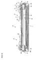
- FIG. 1 is a horizontal sectional view of a liquid crystal display device (a display device) D of the present embodiment.
- FIG. 2 is a perspective view of a lighting device (a lighting device for a display device) 10 included in the liquid crystal display device D.
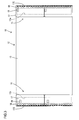
- FIG. 3 is a rear elevational view of the lighting device 10.
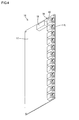
- FIG. 4 is a perspective view of a power board (a circuit board) 16 included in the lighting device 10.
- FIG. 5 is a front elevational view of the power board 16.
- FIG. 6 is a perspective view of a discharge tube 15.
- FIG. 7 is an explanatory diagram schematically showing a drive power supply structure for discharge tubes 15.
- FIG. 8 is an explanatory diagram schematically showing a modification of the drive power supply structure for discharge tubes 15.
- FIG. 9 is a schematic diagram separately showing the construction of the supply structure.
- FIG. 10 is a horizontal sectional view of a modification of the liquid crystal display device D.
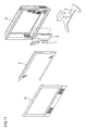
- FIG. 11 is an exploded perspective view of an embodiment of a television receiver.
- the liquid crystal display device D shown in FIG. 1 forms a horizontally-long rectangular shape as a whole, which includes a display panel 11 and a lighting device 10 as shown in FIG. 1 .
- the display panel 11 is disposed on the front side of the lighting device 10, so that the lighting device 10 as a backlight can optically illuminate the display panel 11 from the back.
- the liquid crystal display D can be applied to a television receiver.
- the television receiver includes the liquid crystal display D, and front and back cabinets Ca and Cb capable of holding the liquid crystal display device D therebetween. Further included are a power source P other than a power board 16 described below, a tuner T and a stand S.
- the display panel 11 has a well-known construction, in which liquid crystal as a material with an optical property that changes with applied voltage is filled between a transparent TFT substrate and a transparent CF substrate.
- TFTs Thin Film Transistors
- a color filter on which color sections of three primary colors, i.e., Red (R), Green (G) and Blue (B), are arranged in a matrix, and the opposite electrodes are provided on the CF substrate.
- the lighting device 10 includes a lamp unit 12 and power boards 16, as shown in FIG. 2 in detail.
- the lamp unit 12 includes a metallic chassis 13, which forms a horizontally-long rectangular plate as a whole and functions as a reflector plate. Further included are a plurality of discharge tubes 15 vertically arranged on the front side of the chassis 13 and held in a horizontal position, and a plurality of relay connectors 14 which are vertically arranged along the lateral edges of the chassis 13 so as to correspond to the respective discharge tubes 15.
- the power boards 16 are disposed on the back side of the chassis 13 so as to supply power to the discharge tubes 15 via the relay connectors 14.
- a plurality of mounting holes 13H corresponding to the ends of the discharge tubes 15 are formed through the chassis 13 so as to extend from the front side to the back side, and are arranged vertically so as to be level with the respective discharge tubes 15.
- the relay connectors 14 are mounted through the respective mounting holes 13H.
- Each relay connector 14 includes a metallic holder (holder electrode) 180 having conductivity.
- the discharge tube 15 can be mounted to the chassis 13 via the holder 180.
- the holder 180 can be formed as a clip, for example, so as to be able to hold a ferrule (a terminal) 50 provided on the end of the discharge tube 15. That is, a pair of elastic locking parts is formed so that the discharge tube 15 can be freely inserted into or removed from the holder 180 due to elastic deformation of the elastic locking parts.
- the holder 180 is inserted into the mounting hole 13H from the front side of the chassis 13, and fixed to the chassis 13.
- the front end portion of the holder 180 projects from the front side of the chassis 13 while the back end portion thereof projects from the back side of the chassis 13, when the holder 180 is attached to the chassis 13.
- the back end portion of the holder 180 is connected to the power board 16 in order to form an electrical connection.
- the holder 180 has conductivity as described above. Therefore, as well as having a function for holding the discharge tube 15, the holder 180 functions as an electrode, through which the discharge tube 15 is electrically connected to the power board 16 so that drive power can be supplied to the discharge tube 15.
- openings 13a are formed on some areas of the chassis 13.
- the openings 13a are arranged on the chassis 13 so as to overlap with or be opposed to the power boards 16. Thereby, isolation between the power boards 16 and the inside of the chassis 13 can be achieved.
- each discharge tube 15 is formed as a cold cathode fluorescent tube having discharge gas in a glass tube, which includes the generally elongated straight glass tube 40 having a circular cross section, elongated outer leads 42 projecting linearly from the respective ends of the glass tube 40 and coaxially with the glass tube 40, and ferrules 50 attached to the respective end portions of the glass tube 40.
- Each ferrule 50 includes a body 51 and a conductive part 57, and can be formed by bending or hammering, using a metallic (e.g., copper alloy) plate that is formed into a predetermined shape by punching.
- the body 51 forms a cylindrical shape as a whole, and is mounted to the periphery of the glass tube 40.
- the conductive part 57 extends from the end edge of the body 51 so as to have elastic contact with the periphery of the outer lead 42, and is fixed by welding.
- each discharge tube 15 having the above construction can be fitted into the holders 180 on its respective ends, so as to be mounted to the chassis 13.
- the holders 180 have elastic contact with the peripheries of the bodies 51 of the respective ferrules 50, so that drive power can be supplied thereto via the holders 180. That is, each ferrule 50 forms a power connecting terminal (a terminal) of the discharge tube 15.
- installation and electrical connection of the discharge tube 15 can be completed merely by fitting its ferrules 50 into the holders 180.
- each power board 16 disposed on the back side of the chassis 13 includes a base member 17 having a circuit formed on its back side (i.e., on the opposite side of the chassis 13), an inverter circuit component 19 mounted on the back side of the base member 17, and a plurality of on-board connectors 18 mounted on the back side of the base member 17.
- the inverter circuit component 19, i.e., a circuit component for providing drive power for the discharge tubes 15 in the present embodiment, has a function for adjusting the supply voltage to (or generating a higher voltage of) a predetermined voltage level.
- the base member 17 forms a vertically-long rectangular shape as a whole, which is formed using a phenolic paper-base copper-clad laminated board (known as a phenolic paper).
- a plurality of fitting holes 17H having a vertically-long rectangular shape are formed through the base member 17 so as to extend from the front side to the back side.
- the plurality of fitting holes 17H are arranged vertically along the lateral side edge 17E (i.e., outer side edge) of the base member 17 so as to correspond to the relay connectors 14.
- a plurality of locating holes 17a are formed through the base member 17 so as to extend from the front side to the back side.
- the locating holes 17a are arranged between the fitting holes 17H and the lateral side of the base member 17 so that a pair of upper and lower locating holes corresponds to each fitting hole 17H.
- the on-board connectors 18 are arranged along the lateral side of the base member 17 so as to correspond to the respective fitting holes 17H, and are engaged with the respective relay connectors 14 through the fitting holes 17H.
- Each on-board connector 18 includes a housing 60 (See FIG. 4 ) made of an insulating material such as a synthetic resin, and the holder 180 held in the housing 60.
- the holders 180 are electrically connected to the inverter circuit component 19 within the base member 17. As described above, the holders 180 function as electrodes through which drive power is supplied to the discharge tubes 15, while holding the discharge tubes 15 within the chassis 13. Specifically, as shown in FIG. 5 , a common electrode 110 is provided so that the inverter circuit component 19 is allowed to provide drive power concurrently for the holders 180. The drive power is supplied from the common electrode 110 individually to the holders 180 via a dielectric film 100.
- the common electrode 110 is formed of a conductive thin film such as an aluminum film.
- the dielectric film 100 is formed of a thin film made of an insulating material such as ceramics.
- the dielectric film 100 is shared by the holders 180, and therefore is formed solidly so as to extend across the holders 180.
- the plurally-arranged discharge tubes 15 differ in electrical potential, and therefore drive power supplied thereto should differ in level.
- inverter circuit components 19 should be provided individually for the respective discharge tubes 15, in order to provide drive power at different levels for the discharge tubes 15 (i.e., for the holders 180 in the present embodiment).
- drive power from the common electrode 110 is supplied, via the dielectric film (dielectric portion) 100, to the holders 180 that function as electrodes of the discharge tubes 15. Therefore, the drive power can be supplied at a fixed level to the common electrode 110. That is, the discharge tubes 15 can share the inverter circuit component 19.
- an inverter circuit component 19 is provided on each of four power boards 16, which are provided on the back side of the chassis 13.
- a capacitor is formed of the dielectric film 100 disposed between the holder (the holder electrode) 180 and the common electrode 110, as shown in FIG. 7 .
- the capacitor can adjust (or limit) the drive power to be supplied to the discharge tube 15, to a predetermined voltage level. Due to the capacitors thus formed, the discharge tubes 15 form a system capable of being driven in parallel. That is, the drive therefor can be achieved by use of a common inverter circuit component 19 as a power source.
- the liquid crystal display device D of the present embodiment having the above construction develops the following operational effects.
- the holders 180 for holding the discharge tubes 15 function as electrodes on the route of drive power supply for the discharge tubes 15. Further, the holders 180 are directly connected to the power boards 16 disposed on the back side of the chassis 13. According to this construction, a harness for power supply can be eliminated, and the power-supply-related construction can be greatly simplified. Further, mounting of the discharge tubes 15 and wiring therefor can be significantly facilitated.
- the drive power is supplied from the common electrode 110 to the holders 180 via the dielectric film 100, and consequently the discharge tubes 15 can be driven in parallel. That is, parallel drive for the discharge tubes 15 can be allowed due to a capacitance formed between a power source (e.g., the inverter circuit component 19 in the present embodiment) and each discharge tube 15.
- a power source e.g., the inverter circuit component 19 in the present embodiment
- the drive power is supplied to the common electrode 110 at a common voltage level, while the drive power therefrom is supplied, via the dielectric film 110, individually to the respective holders 180 and therefore to the respective discharge tubes 15 which are connected in parallel thereto.
- a capacitance formed of the dielectric film 100 disposed between the common electrode 110 and the holders 180 can adjust (or limit) the voltage level, so that the drive power is supplied to each holder 180 at a proper level.
- parallel drive for the discharge tubes 15 can be achieved by a simple construction including the holders 180, resulting in contribution to large cost reduction.
- the holders 180 are provided on the respective ends of each discharge tube 15, as shown in FIG. 7 . Thereby, the voltage is applied to each discharge tube 15 in a balanced manner, resulting in improved luminous efficiency.
- the chassis 13 of the liquid crystal display device D includes openings 13a, which are formed so as to overlap with the power boards 16. Thereby, electrical leakage from the power boards 16 into the chassis 13 can be prevented or suppressed. That is, the power boards 16 generate or provide a high-frequency voltage, and therefore electrical leakage, or the like, into the chassis 13 can be prevented or suppressed by forming the openings 13a on the chassis 13.
- the openings 13a further have a function for preventing heat conduction from the power boards 16 prone to high temperature into the chassis 13a.
- the prevention of electrical leakage and heat conduction can be achieved by concave portions lower than the rest thereof, which are formed on the chassis 13 so as to overlap with the power boards 16.
- a capacitor chip 101 may be disposed between the common electrode 111 and each holder 180, as shown in FIG. 8 . That is, the dielectric film 100 is disposed between the common electrode 111 and the holders 180 in the embodiment shown in FIG. 1 , in order to provide a capacitance capable of adjusting (or limiting) the voltage level applied to each discharge tube 15.
- the capacitance may be formed of a capacitor chip 101. If the capacitances are thus formed of capacitor chips 101, manufacturing efficiency can be improved, resulting in contribution to cost reduction. Note that the capacitances 101 are provided so as to correspond one-to-one with the holders 180 as shown in FIG. 9 , in this case.
- the electrical and heat isolation between the power boards 16 and the chassis 13 can be achieved by electrical and heat insulating members 130, as shown in FIG. 10 . That is, the electrical and heat isolation between the power boards 16 and the chassis 13 is achieved by forming the openings 13a on the chassis 13, in the embodiment shown in FIG. 1 . Alternatively, the electrical and heat isolation may be achieved by providing the electrical and heat insulating members 130 therebetween. In this case, preferably, members made of ceramics such as alumina are used as the electrical and heat insulating members 130.
- each power board 16 is not limited to a phenolic paper-base copper-clad laminated board, but rather may be formed of a plate made of glass epoxy or ceramics.
- the display panel 11 of the liquid crystal display device D is not limited to having TFTs as switching elements, but rather may include, as switching elements, elements other than TFTs such as MIM (Metal Insulator Metal) elements.
- the display device of the present invention is not limited to the liquid crystal display device. Various display devices requiring a lighting device on the back side of a display panel can be included.
- the capacitive coupling between the common electrode 111 and each holder (holder electrode) 180 can be achieved by mounting a chip capacitor (dielectric element) 201 as a dielectric portion on the circuit board (paper phenol substrate) 200.
- holders (holder electrodes) 180 are mounted on the circuit board 200, and the common electrode 111 is electrically connected to each holder 180 via a chip capacitor 201, as shown in the figure. That is, the chip capacitors 201 are mounted on the circuit board 200 so as to correspond one-to-one with the holders 180.
- the electrical connection between the common electrode 110a and each holder (holder electrode) 180 can be formed by use of a circuit board (a glass-epoxy substrate) 100a as a dielectric portion.
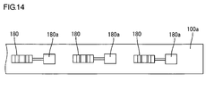
- holders 180 and first-capacity electrodes 180a equipotent to the respective holders 180 are formed on the upper surface (a first surface) of the circuit board 100a, as shown also in FIG. 14 .
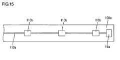
- Second-capacity electrodes 110b arranged on the opposite side of the circuit board 100a from the first-capacity electrodes 180a, and the common electrode (a common wiring line) 110a equipotent to the second-capacity electrodes 110b are formed on the lower surface (a second surface) of the circuit board 100a, as shown also in FIG. 15 .
- the common electrode 110a is electrically connected to the terminal 19a of the inverter board 19.
- the electrical connection between the common electrode 110a and each holder (holder electrode) 180 can be formed by use of a circuit board (a glass-epoxy substrate) 100a as a dielectric portion.
- holders 180, third-capacity electrodes 110c disconnected from the holders 180, and the common electrode (a common wiring line) 110a equipotent to the third-capacity electrodes 110 are formed on the upper surface (a first surface) of the circuit board 100a, as shown also in FIG. 17 .
- the common electrode 110a is electrically connected to the terminal 19a of the inverter board 19.
- the lead wires (connecting terminal portions) 180m of the holders 180 penetrating the circuit board 100a from the upper side, and fourth-capacity electrodes 180n connected to the lead wires 180m so as to be equipotent to the respective holders 180, are formed on the lower surface (a second surface) of the circuit board 100a, as shown also in FIG. 18 .
- the parallel coupling can be readily achieved by forming a wiring pattern on the circuit board 100a so that the capacitors are provided.
- the lead wires 180m and the fourth-capacity electrodes 180n on the lower surface of the circuit board 100a are isolated from the chassis 13, in the construction shown in FIG. 16 .
- the isolation can be achieved by forming slit-like openings on the chassis 13, which are opposed to the lead wires 180m and the fourth-capacity electrodes 180n. Further, note that the common electrode 110a is wired so as to bypass the holders 180 for isolation therefrom.
Landscapes
- Physics & Mathematics (AREA)
- Nonlinear Science (AREA)
- Engineering & Computer Science (AREA)
- Mathematical Physics (AREA)
- Chemical & Material Sciences (AREA)
- Crystallography & Structural Chemistry (AREA)
- General Physics & Mathematics (AREA)
- Optics & Photonics (AREA)
- Electromagnetism (AREA)
- Plasma & Fusion (AREA)
- General Engineering & Computer Science (AREA)
- Planar Illumination Modules (AREA)
- Liquid Crystal (AREA)
- Fastening Of Light Sources Or Lamp Holders (AREA)
- Arrangement Of Elements, Cooling, Sealing, Or The Like Of Lighting Devices (AREA)
- Circuit Arrangements For Discharge Lamps (AREA)
- Connecting Device With Holders (AREA)
- Devices For Indicating Variable Information By Combining Individual Elements (AREA)
- Electroluminescent Light Sources (AREA)
- Transforming Electric Information Into Light Information (AREA)
Abstract
Description
- The present invention relates to a lighting device for a display device, a display device and a television receiver.
- In a display device having non-luminous optical elements as typified by a liquid crystal display device, a backlight device is provided on the backside of a display panel such as a liquid crystal panel, so as to illuminate the display panel (as shown in Patent Document 1, for example).
- Patent Document 1:
JP-A-2006-245005 - The backlight device, disclosed in Patent Document 1, has a structure that enables parallel drive for CCFLs. That is, a lamp drive device is disclosed in Patent Document 1, which includes a plurality of cold cathode fluorescent lamps connected in parallel, a first current limiting unit connected to the plurality of CCFLs for controlling the magnitude of power to be supplied so as to discharge the CCFLs, and an inverter for changing the magnitude of received AC power and supplying the changed AC power to the first current limiting unit. The parallel drive structure for CCFLs enables minimization of defective fraction as well as reduction in production costs of CCFLs. However, Patent Document 1 fails to disclose the details of the structure. That merely discloses that the first current limiting unit specifically includes ballast capacitors.
- An object of the present invention is to enable parallel drive for light sources by a simplified parallel drive structure so as to contribute to large cost reduction, and thereby provide a failure-resistant and highly-reliable lighting device for a display device. Another object of the present invention is to provide a display device having the lighting device for a display device, and to provide a television receiver having the display device.
- In order to solve the above problem, a lighting device for a display device according to the present invention includes a plurality of light sources, a power source for providing drive power for the light source, a common electrode for supplying the drive power to the plurality of light sources, a plurality of holder electrodes for holding the respective light sources and supplying the drive power from the common electrode individually to the respective light sources, and a dielectric portion provided between the common electrode and each of the holder electrodes.
- According to this construction, the lighting device for a display device includes electrodes, to which drive power is supplied via the common electrode and the dielectric portion, and from which the drive power is supplied individually to the respective light sources. The electrodes are provided as holder electrodes capable of holding the respective light sources, i.e., provided as a simplified construction in which a holder function and an electrode function for light sources are combined. Thereby, the trouble of wiring or installation of light sources can be saved, and therefore manufacturing efficiency could be improved, resulting in contribution to cost reduction. Further, wiring or mounting-related failures are unlikely to occur, which could result in a highly-reliable lighting device for a display device.
Moreover, the dielectric portion is provided between the common electrode and each holder electrode. Thereby, a capacitance is provided between the power source and each light source, and consequently parallel drive for the light sources is allowed. That is, the drive power from the power source is supplied to the common electrode at a common voltage level, while the drive power therefrom is supplied, via the dielectric portion, individually to the respective holder electrodes and therefore to the respective light sources which are connected in parallel thereto. Consequently, the drive power can be supplied to each light source at a proper level, because the capacitance adjusts (or limits) the voltage level.
Thus, according to the present invention, parallel drive for light sources can be achieved by a simple construction including holder electrodes, resulting in contribution to cost reduction for a lighting device for a display device and therefore cost reduction for a display device. - The light source can be formed of a discharge tube.
The level of a voltage to be supplied to the light source formed of a discharge tube should be adjusted individually. According to the present invention, the intervening dielectric portion is provided, and thereby the level of a voltage to be supplied to the light source can be adjusted suitably. - The power source can include an inverter circuit that generates a high-frequency voltage.
According to the present invention, a voltage can be supplied at a fixed level to the common electrode. Therefore, the present invention is suitable for a construction including an inverter circuit that generates a high-frequency voltage, because the need for inverter circuits provided individually for the light sources can be eliminated resulting in a simple construction. - The common electrode can be provided so as to be capable of supplying the drive power concurrently to the plurality of light sources.
According to the present invention, the common electrode is provided so as to be connected to the respective light sources via the dielectric portion and the respective holder electrodes. Thereby, the common electrode is allowed to supply drive power concurrently to the plurality of light sources, and therefore drive power can be supplied from the power source to the common electrode at a predetermined level. Consequently, the number of above-described inverter circuits can be reduced to one, for example. Thus, the construction of the lighting device for a display device can be simplified. - The light source can include a terminal for receiving supply of the drive power, while the holder electrode can be provided so as to be capable of holding the terminal and supplying the drive power via the terminal.
If the terminal of a light source and a holder electrode capable of holding the terminal are thus provided, wiring can be eliminated and thereby the construction for light source drive can be greatly simplified. - The light source can include a terminal for receiving supply of the drive power, while the holder electrode can be formed of a conductive clip member capable of holding the terminal.
If the terminal of a light source and a holder electrode formed of a conductive clip member capable of holding the terminal are thus provided, wiring can be eliminated and thereby the construction for light source drive can be greatly simplified. - The light source can be provided as a linear light source, so that terminals for receiving supply of the drive power are provided on respective ends of the linear light source while the holder electrode is provided for each of the terminals on the respective ends.
According to the construction in which the holder electrodes of the present invention are thus provided so as to hold the terminals on the respective ends of a linear light source, a voltage can be applied to the ends of the light source in a balanced manner, resulting in improved luminous efficiency. - The light source can include a straight glass tube, outer leads projecting linearly from respective ends of the glass tube and coaxially with the glass tube, and ferrules which are electrically connected to the outer leads and are mounted to respective end portions of the glass tube so as to form the above terminal.
In the case that each light source thus includes outer leads and ferrules on the respective ends of its straight glass tube, according to the present invention which includes holder electrodes, installation and electrical connection of the light sources can be simultaneously achieved. Further, parallel drive for the light sources is allowed, because the common electrode is provided so as to be connected to the holder electrodes via the dielectric portion. Thus, the construction can be simplified, resulting in further contribution to cost reduction. - The dielectric portion can be a dielectric film provided between the common electrode and the holder electrode.
According to this construction, the capacitance can be formed readily and reliably. If the holder electrodes are provided specifically on the dielectric film that can be formed on the common electrode in layers, manufacturing efficiency can be further improved, resulting in contribution to cost reduction. - The dielectric portion can be a capacitor chip provided between the common electrode and the holder electrode.
According to this construction, the capacitance can be formed readily and reliably. Manufacturing efficiency can be further improved particularly due to capacitor chips, resulting in contribution to cost reduction. - A chassis for containing the light source, and a circuit board disposed on the opposite side of the chassis from the light source can be further included, so that the common electrode, the holder electrode and the dielectric portion are formed on the circuit board while an insulating member is provided between the chassis and the circuit board.
The circuit board including the common electrode and the holder electrode may generate or provide a high-frequency voltage. Therefore, it is preferable to provide an insulating member in order to prevent or suppress electrical leakage, or the like, into the chassis. If the chassis is specifically formed of a metallic plate or the like, the effect of providing the insulating member can be further pronounced because of the conductivity of the chassis. - In addition, the circuit board can reach high temperature due to the high-frequency voltage. In view of this, a heat insulating member may be provided between the circuit board and the chassis. In this case, an electrical and heat insulating member can be used, for example.
- A chassis for containing the light source, and a circuit board disposed on the opposite side of the chassis from the light source can be further included, so that the common electrode, the holder electrode and the dielectric portion are formed on the circuit board while an opening is formed on the chassis so as to overlap with the circuit board.
The circuit board including the common electrode and the holder electrode may generate or provide a high-frequency voltage. Therefore, it is preferable to provide an opening in order to prevent or suppress electrical leakage, or the like, into the chassis. If the chassis is specifically formed of a metallic plate or the like, the effect of providing the opening can be further pronounced because of the conductivity of the chassis. - A chassis for containing the light source, and a circuit board disposed on the opposite side of the chassis from the light source can be further included, so that the common electrode, the holder electrode and the dielectric portion are formed on the circuit board while a depressed portion lower than the other portions is formed on the chassis so as to overlap with the circuit board.
The circuit board including the common electrode and the holder electrode may generate or provide a high-frequency voltage.
Therefore, in order to prevent or suppress electrical leakage, or the like, into the chassis, it is preferable to provide a depressed portion so as to keep a distance therefrom. If the chassis is specifically formed of a metallic plate or the like, the effect of providing the depressed portion can be further pronounced because of the conductivity of the chassis. - In order to solve the above problem, a display device of the present invention includes the above lighting device for a display device according to the present invention, and a display panel for providing display by use of light from the lighting device for a display device.
In the case of a display device having the above construction, cost reduction and reliability improvement can be achieved for the lighting device for a display device, and therefore cost reduction and reliability improvement can be also achieved for the display device - A liquid crystal panel can exemplify the above display panel. The display device as a liquid crystal display device has a variety of applications, such as a television display or a personal-computer display. Particularly, it is suitable for a large screen display.
- A television receiver of the present invention includes the above display device.
According to this construction, a highly-reliable television receiver can be provided inexpensively. - The present invention enables parallel drive for light sources by a simplified parallel drive structure, so as to contribute to large cost reduction. Thereby, a failure-resistant and highly-reliable lighting device for a display device can be provided. Further, an inexpensive and highly-reliable display device having the lighting device for a display device, and an inexpensive and highly-reliable television receiver having the display device can be provided.
-
- [
FIG. 1 ] is a horizontal sectional view of a liquid crystal display device (a display device) according to an embodiment; - [
FIG. 2 ] is a perspective view of a lighting device (a lighting device for a display device) included in the liquid crystal display device; - [
FIG. 3 ] is a rear elevational view of the lighting device; - [
FIG. 4 ] is a perspective view of a power board (circuit board) included in the lighting device; - [
FIG. 5 ] is a front elevational view of the power board; - [
FIG. 6 ] is a perspective view of a discharge tube; - [
FIG. 7 ] is an explanatory diagram schematically showing a drive power supply structure for discharge tubes; - [
FIG. 8 ] is an explanatory diagram schematically showing a modification of the drive power supply structure for discharge tubes; - [
FIG. 9 ] is a schematic diagram separately showing the construction of the supply structure shown inFIG. 8 ; - [
FIG. 10 ] is a horizontal sectional view of a modification of the liquid crystal display device; - [
FIG. 11 ] is an exploded perspective view of an embodiment of a television receiver; - [
FIG. 12 ] is an explanatory diagram schematically showing a modification of the drive power supply structure for discharge tubes; - [
FIG. 13 ] is an explanatory diagram schematically showing another modification of the drive power supply structure for discharge tubes; - [
FIG. 14 ] is a top plan view ofFIG. 13 ; - [
FIG. 15 ] is a bottom plan view ofFIG. 13 ; - [
FIG. 16 ] is an explanatory diagram schematically showing another modification of the drive power supply structure for discharge tubes; - [
FIG. 17 ] is a top plan view ofFIG. 16 ; and - [
FIG. 18 ] is a bottom plan view ofFIG. 16 . - 10···Lighting device (Lighting device for display device), 15···Discharge tube (Light source) , 19···Inverter circuit component (Power source) , T···Power source, 100···Dielectric film (Dielectric portion), 110, 111··· Common electrode, 180··· Holder (Holder electrode)
- Hereinafter, an embodiment of the present invention will be explained with reference to the drawings.
FIG. 1 is a horizontal sectional view of a liquid crystal display device (a display device) D of the present embodiment.
FIG. 2 is a perspective view of a lighting device (a lighting device for a display device) 10 included in the liquid crystal display device D.FIG. 3 is a rear elevational view of thelighting device 10.FIG. 4 is a perspective view of a power board (a circuit board) 16 included in thelighting device 10.FIG. 5 is a front elevational view of thepower board 16.FIG. 6 is a perspective view of adischarge tube 15.FIG. 7 is an explanatory diagram schematically showing a drive power supply structure fordischarge tubes 15. -
FIG. 8 is an explanatory diagram schematically showing a modification of the drive power supply structure fordischarge tubes 15.FIG. 9 is a schematic diagram separately showing the construction of the supply structure.FIG. 10 is a horizontal sectional view of a modification of the liquid crystal display device D.FIG. 11 is an exploded perspective view of an embodiment of a television receiver. - The liquid crystal display device D shown in
FIG. 1 forms a horizontally-long rectangular shape as a whole, which includes adisplay panel 11 and alighting device 10 as shown inFIG. 1 . Thedisplay panel 11 is disposed on the front side of thelighting device 10, so that thelighting device 10 as a backlight can optically illuminate thedisplay panel 11 from the back. - The liquid crystal display D can be applied to a television receiver. As shown in
FIG. 11 , the television receiver includes the liquid crystal display D, and front and back cabinets Ca and Cb capable of holding the liquid crystal display device D therebetween. Further included are a power source P other than apower board 16 described below, a tuner T and a stand S. - The
display panel 11 has a well-known construction, in which liquid crystal as a material with an optical property that changes with applied voltage is filled between a transparent TFT substrate and a transparent CF substrate. TFTs (Thin Film Transistors), as switching elements connected to a source wiring line and a gate wiring line running at right angles to each other, and pixel electrodes are provided on the TFT substrate. A color filter, on which color sections of three primary colors, i.e., Red (R), Green (G) and Blue (B), are arranged in a matrix, and the opposite electrodes are provided on the CF substrate. - The
lighting device 10 includes alamp unit 12 andpower boards 16, as shown inFIG. 2 in detail.
Thelamp unit 12 includes ametallic chassis 13, which forms a horizontally-long rectangular plate as a whole and functions as a reflector plate. Further included are a plurality ofdischarge tubes 15 vertically arranged on the front side of thechassis 13 and held in a horizontal position, and a plurality ofrelay connectors 14 which are vertically arranged along the lateral edges of thechassis 13 so as to correspond to therespective discharge tubes 15.
Thepower boards 16 are disposed on the back side of thechassis 13 so as to supply power to thedischarge tubes 15 via therelay connectors 14. - A plurality of mounting
holes 13H corresponding to the ends of thedischarge tubes 15 are formed through thechassis 13 so as to extend from the front side to the back side, and are arranged vertically so as to be level with therespective discharge tubes 15. Therelay connectors 14 are mounted through the respective mountingholes 13H. Eachrelay connector 14 includes a metallic holder (holder electrode) 180 having conductivity. Thedischarge tube 15 can be mounted to thechassis 13 via theholder 180. - As shown in
FIG. 7 , theholder 180 can be formed as a clip, for example, so as to be able to hold a ferrule (a terminal) 50 provided on the end of thedischarge tube 15. That is, a pair of elastic locking parts is formed so that thedischarge tube 15 can be freely inserted into or removed from theholder 180 due to elastic deformation of the elastic locking parts. - The
holder 180 is inserted into the mountinghole 13H from the front side of thechassis 13, and fixed to thechassis 13. The front end portion of theholder 180 projects from the front side of thechassis 13 while the back end portion thereof projects from the back side of thechassis 13, when theholder 180 is attached to thechassis 13. The back end portion of theholder 180 is connected to thepower board 16 in order to form an electrical connection. Note that theholder 180 has conductivity as described above. Therefore, as well as having a function for holding thedischarge tube 15, theholder 180 functions as an electrode, through which thedischarge tube 15 is electrically connected to thepower board 16 so that drive power can be supplied to thedischarge tube 15. - As shown in
FIGS. 2 and3 ,openings 13a are formed on some areas of thechassis 13. Theopenings 13a are arranged on thechassis 13 so as to overlap with or be opposed to thepower boards 16. Thereby, isolation between thepower boards 16 and the inside of thechassis 13 can be achieved. - Referring to
FIG. 6 , eachdischarge tube 15 is formed as a cold cathode fluorescent tube having discharge gas in a glass tube, which includes the generally elongatedstraight glass tube 40 having a circular cross section, elongated outer leads 42 projecting linearly from the respective ends of theglass tube 40 and coaxially with theglass tube 40, andferrules 50 attached to the respective end portions of theglass tube 40. Eachferrule 50 includes abody 51 and aconductive part 57, and can be formed by bending or hammering, using a metallic (e.g., copper alloy) plate that is formed into a predetermined shape by punching. Thebody 51 forms a cylindrical shape as a whole, and is mounted to the periphery of theglass tube 40. Theconductive part 57 extends from the end edge of thebody 51 so as to have elastic contact with the periphery of theouter lead 42, and is fixed by welding. - As shown in
FIG. 7 , eachdischarge tube 15 having the above construction can be fitted into theholders 180 on its respective ends, so as to be mounted to thechassis 13. Theholders 180 have elastic contact with the peripheries of thebodies 51 of therespective ferrules 50, so that drive power can be supplied thereto via theholders 180. That is, eachferrule 50 forms a power connecting terminal (a terminal) of thedischarge tube 15. Thus, installation and electrical connection of thedischarge tube 15 can be completed merely by fitting itsferrules 50 into theholders 180. - On the other hand, as shown in
FIGS. 1 ,3 to 5 , eachpower board 16 disposed on the back side of thechassis 13 includes abase member 17 having a circuit formed on its back side (i.e., on the opposite side of the chassis 13), aninverter circuit component 19 mounted on the back side of thebase member 17, and a plurality of on-board connectors 18 mounted on the back side of thebase member 17. Theinverter circuit component 19, i.e., a circuit component for providing drive power for thedischarge tubes 15 in the present embodiment, has a function for adjusting the supply voltage to (or generating a higher voltage of) a predetermined voltage level. - The
base member 17 forms a vertically-long rectangular shape as a whole, which is formed using a phenolic paper-base copper-clad laminated board (known as a phenolic paper). A plurality offitting holes 17H having a vertically-long rectangular shape are formed through thebase member 17 so as to extend from the front side to the back side. The plurality offitting holes 17H are arranged vertically along thelateral side edge 17E (i.e., outer side edge) of thebase member 17 so as to correspond to therelay connectors 14. Further, a plurality of locatingholes 17a are formed through thebase member 17 so as to extend from the front side to the back side. The locatingholes 17a are arranged between thefitting holes 17H and the lateral side of thebase member 17 so that a pair of upper and lower locating holes corresponds to eachfitting hole 17H. - The on-
board connectors 18 are arranged along the lateral side of thebase member 17 so as to correspond to the respectivefitting holes 17H, and are engaged with therespective relay connectors 14 through thefitting holes 17H. Each on-board connector 18 includes a housing 60 (SeeFIG. 4 ) made of an insulating material such as a synthetic resin, and theholder 180 held in thehousing 60. - The
holders 180 are electrically connected to theinverter circuit component 19 within thebase member 17. As described above, theholders 180 function as electrodes through which drive power is supplied to thedischarge tubes 15, while holding thedischarge tubes 15 within thechassis 13.
Specifically, as shown inFIG. 5 , acommon electrode 110 is provided so that theinverter circuit component 19 is allowed to provide drive power concurrently for theholders 180. The drive power is supplied from thecommon electrode 110 individually to theholders 180 via adielectric film 100. - The
common electrode 110 is formed of a conductive thin film such as an aluminum film. Thedielectric film 100 is formed of a thin film made of an insulating material such as ceramics. Thedielectric film 100 is shared by theholders 180, and therefore is formed solidly so as to extend across theholders 180. - The plurally-arranged
discharge tubes 15 differ in electrical potential, and therefore drive power supplied thereto should differ in level. Generally,inverter circuit components 19 should be provided individually for therespective discharge tubes 15, in order to provide drive power at different levels for the discharge tubes 15 (i.e., for theholders 180 in the present embodiment).
However, in the present embodiment, drive power from thecommon electrode 110 is supplied, via the dielectric film (dielectric portion) 100, to theholders 180 that function as electrodes of thedischarge tubes 15. Therefore, the drive power can be supplied at a fixed level to thecommon electrode 110. That is, thedischarge tubes 15 can share theinverter circuit component 19. In the present embodiment, as shown inFIG. 3 , aninverter circuit component 19 is provided on each of fourpower boards 16, which are provided on the back side of thechassis 13. - Specifically, a capacitor is formed of the
dielectric film 100 disposed between the holder (the holder electrode) 180 and thecommon electrode 110, as shown inFIG. 7 . The capacitor can adjust (or limit) the drive power to be supplied to thedischarge tube 15, to a predetermined voltage level. Due to the capacitors thus formed, thedischarge tubes 15 form a system capable of being driven in parallel. That is, the drive therefor can be achieved by use of a commoninverter circuit component 19 as a power source. - The liquid crystal display device D of the present embodiment having the above construction develops the following operational effects.
In thelighting device 10, theholders 180 for holding thedischarge tubes 15 function as electrodes on the route of drive power supply for thedischarge tubes 15. Further, theholders 180 are directly connected to thepower boards 16 disposed on the back side of thechassis 13. According to this construction, a harness for power supply can be eliminated, and the power-supply-related construction can be greatly simplified. Further, mounting of thedischarge tubes 15 and wiring therefor can be significantly facilitated. - The drive power is supplied from the
common electrode 110 to theholders 180 via thedielectric film 100, and consequently thedischarge tubes 15 can be driven in parallel. That is, parallel drive for thedischarge tubes 15 can be allowed due to a capacitance formed between a power source (e.g., theinverter circuit component 19 in the present embodiment) and eachdischarge tube 15. Specifically, the drive power is supplied to thecommon electrode 110 at a common voltage level, while the drive power therefrom is supplied, via thedielectric film 110, individually to therespective holders 180 and therefore to therespective discharge tubes 15 which are connected in parallel thereto. According to this construction, a capacitance formed of thedielectric film 100 disposed between thecommon electrode 110 and theholders 180 can adjust (or limit) the voltage level, so that the drive power is supplied to eachholder 180 at a proper level. Thus, according to the present embodiment, parallel drive for thedischarge tubes 15 can be achieved by a simple construction including theholders 180, resulting in contribution to large cost reduction. - Further, in the present embodiment, the
holders 180 are provided on the respective ends of eachdischarge tube 15, as shown inFIG. 7 . Thereby, the voltage is applied to eachdischarge tube 15 in a balanced manner, resulting in improved luminous efficiency. - In the present embodiment, the
chassis 13 of the liquid crystal display device D includesopenings 13a, which are formed so as to overlap with thepower boards 16. Thereby, electrical leakage from thepower boards 16 into thechassis 13 can be prevented or suppressed. That is, thepower boards 16 generate or provide a high-frequency voltage, and therefore electrical leakage, or the like, into thechassis 13 can be prevented or suppressed by forming theopenings 13a on thechassis 13. Theopenings 13a further have a function for preventing heat conduction from thepower boards 16 prone to high temperature into thechassis 13a. - Alternatively, the prevention of electrical leakage and heat conduction can be achieved by concave portions lower than the rest thereof, which are formed on the
chassis 13 so as to overlap with thepower boards 16. - This is the end of explanation of the preferred embodiment of the present invention. However, the present invention is not limited to the embodiment explained in the above description made with reference to the drawings. The following embodiments may be included in the technical scope of the present invention, for example.
- (1) A
capacitor chip 101 may be disposed between thecommon electrode 111 and eachholder 180, as shown inFIG. 8 . That is, thedielectric film 100 is disposed between thecommon electrode 111 and theholders 180 in the embodiment shown inFIG. 1 , in order to provide a capacitance capable of adjusting (or limiting) the voltage level applied to eachdischarge tube 15. Alternatively, the capacitance may be formed of acapacitor chip 101.
If the capacitances are thus formed ofcapacitor chips 101, manufacturing efficiency can be improved, resulting in contribution to cost reduction.
Note that thecapacitances 101 are provided so as to correspond one-to-one with theholders 180 as shown inFIG. 9 , in this case. - (2) The electrical and heat isolation between the
power boards 16 and thechassis 13 can be achieved by electrical and heat insulatingmembers 130, as shown inFIG. 10 . That is, the electrical and heat isolation between thepower boards 16 and thechassis 13 is achieved by forming theopenings 13a on thechassis 13, in the embodiment shown inFIG. 1 . Alternatively, the electrical and heat isolation may be achieved by providing the electrical and heat insulatingmembers 130 therebetween. In this case, preferably, members made of ceramics such as alumina are used as the electrical and heat insulatingmembers 130. - (3) The
base member 17 of eachpower board 16 is not limited to a phenolic paper-base copper-clad laminated board, but rather may be formed of a plate made of glass epoxy or ceramics.
(4) Thedisplay panel 11 of the liquid crystal display device D is not limited to having TFTs as switching elements, but rather may include, as switching elements, elements other than TFTs such as MIM (Metal Insulator Metal) elements.
(5) The display device of the present invention is not limited to the liquid crystal display device. Various display devices requiring a lighting device on the back side of a display panel can be included. - (6) As shown in
FIG. 12 , the capacitive coupling between thecommon electrode 111 and each holder (holder electrode) 180 can be achieved by mounting a chip capacitor (dielectric element) 201 as a dielectric portion on the circuit board (paper phenol substrate) 200. In this case, holders (holder electrodes) 180 are mounted on thecircuit board 200, and thecommon electrode 111 is electrically connected to eachholder 180 via achip capacitor 201, as shown in the figure. That is, thechip capacitors 201 are mounted on thecircuit board 200 so as to correspond one-to-one with theholders 180. - (7) As shown in
FIG. 13 , the electrical connection between thecommon electrode 110a and each holder (holder electrode) 180 can be formed by use of a circuit board (a glass-epoxy substrate) 100a as a dielectric portion. In this case,holders 180 and first-capacity electrodes 180a equipotent to therespective holders 180 are formed on the upper surface (a first surface) of thecircuit board 100a, as shown also inFIG. 14 . Second-capacity electrodes 110b arranged on the opposite side of thecircuit board 100a from the first-capacity electrodes 180a, and the common electrode (a common wiring line) 110a equipotent to the second-capacity electrodes 110b are formed on the lower surface (a second surface) of thecircuit board 100a, as shown also inFIG. 15 . On the back side of the board, thecommon electrode 110a is electrically connected to the terminal 19a of theinverter board 19. - (8) As shown in
FIG. 16 , the electrical connection between thecommon electrode 110a and each holder (holder electrode) 180 can be formed by use of a circuit board (a glass-epoxy substrate) 100a as a dielectric portion. In this case,holders 180, third-capacity electrodes 110c disconnected from theholders 180, and the common electrode (a common wiring line) 110a equipotent to the third-capacity electrodes 110 are formed on the upper surface (a first surface) of thecircuit board 100a, as shown also inFIG. 17 . On the back side of the board, thecommon electrode 110a is electrically connected to the terminal 19a of theinverter board 19. On the other hand, the lead wires (connecting terminal portions) 180m of theholders 180 penetrating thecircuit board 100a from the upper side, and fourth-capacity electrodes 180n connected to thelead wires 180m so as to be equipotent to therespective holders 180, are formed on the lower surface (a second surface) of thecircuit board 100a, as shown also inFIG. 18 . Thus, the parallel coupling can be readily achieved by forming a wiring pattern on thecircuit board 100a so that the capacitors are provided. Note that thelead wires 180m and the fourth-capacity electrodes 180n on the lower surface of thecircuit board 100a are isolated from thechassis 13, in the construction shown inFIG. 16 . Specifically, the isolation can be achieved by forming slit-like openings on thechassis 13, which are opposed to thelead wires 180m and the fourth-capacity electrodes 180n. Further, note that thecommon electrode 110a is wired so as to bypass theholders 180 for isolation therefrom.
Claims (20)
- A lighting device for a display device comprising:a plurality of light sources;a power source for providing drive power for said light sources;a common electrode for supplying said drive power to said plurality of light sources;a plurality of holder electrodes for holding said respective light sources and supplying said drive power from said common electrode individually to said respective light sources; anda dielectric portion provided between said common electrode and each of said holder electrodes.
- A lighting device for a display device as in claim 1, wherein said light source is formed of a discharge tube.
- A lighting device for a display device as in claim 1 or 2, wherein said power source includes an inverter circuit that generates a high-frequency voltage.
- A lighting device for a display device as in any one of claims 1 to 3, wherein said common electrode is capable of supplying said drive power concurrently to said plurality of light sources.
- A lighting device for a display device as in any one of claims 1 to 4, wherein:said light source includes a terminal for receiving supply of said drive power; andsaid holder electrode is capable of holding said terminal and supplying said drive power to said light source via said terminal.
- A lighting device for a display device as in any one of claims 1 to 5, wherein:said light source includes a terminal for receiving supply of said drive power; andsaid holder electrode is formed of a conductive clip member capable of holding said terminal.
- A lighting device for a display device as in any one of claims 1 to 6, wherein:said light source is a linear light source, and terminals for receiving supply of said drive power are provided on respective ends of said linear light source; andsaid holder electrode is provided for each of said terminals on said respective ends.
- A lighting device for a display device as in any one of claims 5 to 7, wherein said light source includes a straight glass tube, outer leads projecting linearly from respective ends of said glass tube and coaxially with said glass tube, and ferrules which are electrically connected to said outer leads and are mounted to respective end portions of said glass tube so as to form said terminal.
- A lighting device for a display device as in any one of claims 1 to 8, wherein said dielectric portion is a dielectric film provided between said common electrode and said holder electrode.
- A lighting device for a display device as in any one of claims 1 to 8, wherein said dielectric portion is a chip capacitor provided between said common electrode and said holder electrode.
- A lighting device for a display device as in any one of claims 1 to 8, wherein:said dielectric portion is formed of chip capacitors mounted on a circuit board; andsaid chip capacitors are mounted so as to correspond one-to-one with said holder electrodes.
- A lighting device for a display device as in any one of claims 1 to 8, wherein:said holder electrodes are provided on a substrate;said dielectric portion is formed of dielectric elements connected to said respective holder electrodes; andsaid holder electrodes are connected to said common electrode via said respective dielectric element.
- A lighting device for a display device as in any one of claims 1 to 8, wherein:said holder electrode is provided on a first surface of a circuit board, and a first-capacity electrode equipotent to said holder electrode is provided on said first surface;said common electrode is provided on a second surface of said circuit board on an opposite side of said first surface, and a second-capacity electrode equipotent to said common electrode is provided on said second surface; andsaid first-capacity electrode is disposed on an opposite side of said circuit board from said second-capacity electrode.
- A lighting device for a display device as in any one of claims 1 to 8, wherein:said holder electrode is provided on a first surface of a circuit board, and further a common electrode isolated from said holder electrode and a third-capacity electrode equipotent to said common electrode is provided on said first surface;a connecting terminal portion, which is formed as a terminal portion of said holder electrode so as to penetrate said circuit board, and a fourth-capacity electrode equipotent to said connecting terminal portion is provided on a second surface of said circuit board on an opposite side of said first surface; andsaid third-capacity electrode is disposed on an opposite side of said circuit board from said fourth-capacity electrode.
- A lighting device for a display device as in any one of claims 1 to 14, further comprising:a chassis for containing said light source; anda circuit board that is disposed on an opposite side of said chassis from said light source and includes said common electrode, said holder electrode and said dielectric portion formed thereon;wherein an insulating member is provided between said chassis and said circuit board.
- A lighting device for a display device as in any one of claims 1 to 14, further comprising:a chassis for containing said light source; anda circuit board that is disposed on an opposite side of said chassis from said light source and includes said common electrode, said holder electrode and said dielectric portion formed thereon;wherein an opening is formed on said chassis so as to overlap with said circuit board.
- A lighting device for a display device as in any one of claims 1 to 14, further comprising:a chassis for containing said light source; anda circuit board that is disposed on an opposite side of said chassis from said light source and includes said common electrode, said holder electrode and said dielectric portion formed thereon;wherein a depressed portion lower than the other portions is formed on said chassis so as to overlap with said circuit board.
- A display device comprising:a lighting device for a display device as in any one of claims 1 to 17; anda display panel for providing display by use of light from said lighting device for a display device.
- A display device as in claim 18, wherein said display panel is a liquid crystal panel that uses liquid crystal.
- A television receiver comprising a display device as in claim 18 or 19.
Applications Claiming Priority (2)
| Application Number | Priority Date | Filing Date | Title |
|---|---|---|---|
| JP2007035192 | 2007-02-15 | ||
| PCT/JP2007/070057 WO2008099532A1 (en) | 2007-02-15 | 2007-10-15 | Illuminating apparatus for display device, display device, and television receiver |
Publications (3)
| Publication Number | Publication Date |
|---|---|
| EP1983252A1 true EP1983252A1 (en) | 2008-10-22 |
| EP1983252A4 EP1983252A4 (en) | 2010-12-22 |
| EP1983252B1 EP1983252B1 (en) | 2012-12-12 |
Family
ID=39689787
Family Applications (1)
| Application Number | Title | Priority Date | Filing Date |
|---|---|---|---|
| EP07829791A Not-in-force EP1983252B1 (en) | 2007-02-15 | 2007-10-15 | Illuminating apparatus for display device, display device, and television receiver |
Country Status (8)
| Country | Link |
|---|---|
| US (3) | US7615935B2 (en) |
| EP (1) | EP1983252B1 (en) |
| JP (2) | JP4153028B1 (en) |
| KR (3) | KR20080078069A (en) |
| CN (2) | CN101916698A (en) |
| DE (1) | DE112007000369B4 (en) |
| GB (2) | GB2448094B (en) |
| WO (1) | WO2008099532A1 (en) |
Families Citing this family (20)
| Publication number | Priority date | Publication date | Assignee | Title |
|---|---|---|---|---|
| DE112007000369B4 (en) * | 2007-02-15 | 2010-08-26 | Sharp Kabushiki Kaisha | Lighting device for a display device, display device and television receiver |
| KR101327853B1 (en) * | 2007-06-08 | 2013-11-12 | 엘지디스플레이 주식회사 | Backlight unit and liquid crystal display device using the same |
| KR101494214B1 (en) * | 2007-10-05 | 2015-02-17 | 삼성디스플레이 주식회사 | Backlight assembly and display device using the same |
| WO2009075123A1 (en) * | 2007-12-12 | 2009-06-18 | Sharp Kabushiki Kaisha | Illuminating device, display device and television receiver |
| CN102057216B (en) * | 2008-06-17 | 2013-03-27 | 夏普株式会社 | Light source holder, lighting device, display device and television receiving device |
| WO2010079646A1 (en) * | 2009-01-08 | 2010-07-15 | シャープ株式会社 | Illuminating device, display device and television receiver |
| WO2010092717A1 (en) * | 2009-02-12 | 2010-08-19 | シャープ株式会社 | Illuminating device for display device, display device and television receiver |
| WO2010092719A1 (en) * | 2009-02-12 | 2010-08-19 | シャープ株式会社 | Illuminating device for display device, display device and television receiver |
| US20110279737A1 (en) * | 2009-02-12 | 2011-11-17 | Sharp Kabushiki Kaisha | Lighting device for display device, display device, and television receiver |
| WO2010092718A1 (en) * | 2009-02-12 | 2010-08-19 | シャープ株式会社 | Lighting device for display device, display device, and television receiver |
| US20100214725A1 (en) * | 2009-02-24 | 2010-08-26 | General Electric Company | Parallel printed wiring board for lamp electronic assembly and bracket therefor |
| US8794786B2 (en) | 2009-02-25 | 2014-08-05 | Sharp Kabushiki Kaisha | Lighting device, display device and television receiver |
| WO2010097995A1 (en) * | 2009-02-25 | 2010-09-02 | シャープ株式会社 | Illumination device, display device and television reception device |
| JPWO2010100803A1 (en) | 2009-03-05 | 2012-09-06 | シャープ株式会社 | Lighting device, display device, and television receiver |
| TWI381225B (en) * | 2009-04-08 | 2013-01-01 | Au Optronics Corp | Lamp device and light source module with spiral connecting tube |
| DE202009017664U1 (en) | 2009-11-10 | 2010-05-12 | Vavouras, Alexis | CCFL lighting system |
| JP5387633B2 (en) * | 2011-08-05 | 2014-01-15 | パナソニック株式会社 | Discharge tube and light emitting device including the discharge tube |
| JP5874059B2 (en) | 2011-11-21 | 2016-03-01 | パナソニックIpマネジメント株式会社 | Organic EL lighting module and lighting apparatus using the same |
| JP2016181624A (en) * | 2015-03-24 | 2016-10-13 | シャープ株式会社 | Heat radiation module and television receiver |
| CN105957787B (en) * | 2016-06-17 | 2024-03-29 | 深圳市槟城电子股份有限公司 | Assembly for gas discharge tube, gas discharge tube and integrated piece thereof |
Family Cites Families (25)
| Publication number | Priority date | Publication date | Assignee | Title |
|---|---|---|---|---|
| JP3532578B2 (en) * | 1991-05-31 | 2004-05-31 | 三菱電機株式会社 | Discharge lamp and image display device using the same |
| JP2001272659A (en) * | 2000-03-24 | 2001-10-05 | Hitachi Ltd | Liquid crystal display |
| US6674250B2 (en) * | 2000-04-15 | 2004-01-06 | Guang-Sup Cho | Backlight including external electrode fluorescent lamp and method for driving the same |
| KR100759362B1 (en) * | 2001-01-18 | 2007-09-19 | 삼성전자주식회사 | Back light assembly and liquid crystal display device having the same |
| US6586863B2 (en) * | 2001-06-28 | 2003-07-01 | Samsung Electro-Mechanics Co., Ltd. | Rosen type piezoelectric transformer with multiple output electrodes |
| EP1296357A2 (en) * | 2001-09-19 | 2003-03-26 | Matsushita Electric Industrial Co., Ltd. | Light source device and liquid crystal display employing the same |
| KR100731304B1 (en) * | 2001-12-19 | 2007-06-21 | 삼성전자주식회사 | Cold cathode ray tube lamp, storage container having same and liquid crystal display having same |
| KR100434331B1 (en) * | 2002-05-22 | 2004-06-04 | 엘지.필립스 엘시디 주식회사 | Back light |
| JP2004220980A (en) * | 2003-01-16 | 2004-08-05 | Tama Electric Co Ltd | Backlight device |
| NZ526028A (en) * | 2003-05-21 | 2006-02-24 | Pure Depth Ltd | Backlighting system for display screen utilised to control the distribution of power to at least one light source |
| JP4554989B2 (en) | 2003-07-30 | 2010-09-29 | パナソニック株式会社 | Cold cathode tube lighting device |
| KR100572140B1 (en) * | 2003-12-12 | 2006-04-24 | 주식회사 엘에스텍 | Direct type backlight device |
| JP4312654B2 (en) * | 2004-05-07 | 2009-08-12 | パナソニック株式会社 | Cold cathode tube lighting device |
| KR101044472B1 (en) * | 2004-06-30 | 2011-06-29 | 엘지디스플레이 주식회사 | Backlight unit for driving multi-lamp and liquid crystal display |
| KR100641005B1 (en) | 2004-07-30 | 2006-11-02 | 엘지.필립스 엘시디 주식회사 | Backlight unit |
| JP4719486B2 (en) * | 2004-10-01 | 2011-07-06 | 三星電子株式会社 | Backlight assembly and display device having the same |
| KR100646427B1 (en) | 2005-03-04 | 2006-11-23 | 삼성전자주식회사 | Lamp coupling structure for parallel drive |
| JP2006344602A (en) * | 2005-06-09 | 2006-12-21 | Samsung Electronics Co Ltd | Lamp, lamp holder, power supply module, backlight assembly having the same, and display device |
| KR20060131248A (en) | 2005-06-15 | 2006-12-20 | 삼성전자주식회사 | Back light assembly and liquid crystal display device having same |
| KR20060131242A (en) * | 2005-06-15 | 2006-12-20 | 삼성전자주식회사 | Cold Cathode Fluorescent Lamp, Manufacturing Method Thereof, Backlight Assembly and Liquid Crystal Display Apparatus |
| JP2007035532A (en) * | 2005-07-29 | 2007-02-08 | Sharp Corp | Backlight device, liquid crystal display device, lamp holder, and assembling method of backlight device |
| TWI311225B (en) * | 2006-01-23 | 2009-06-21 | Chi Mei Optoelectronics Corp | Flat panel display and backlight module thereof |
| CN101201504B (en) * | 2006-12-11 | 2010-10-13 | 乐金显示有限公司 | Backlight unit and liquid crystal display module including the backlight unit |
| EP1933194B1 (en) * | 2006-12-13 | 2014-01-08 | LG Display Co., Ltd. | Backlight unit and liquid crystal display module including the same |
| DE112007000369B4 (en) * | 2007-02-15 | 2010-08-26 | Sharp Kabushiki Kaisha | Lighting device for a display device, display device and television receiver |
-
2007
- 2007-10-15 DE DE112007000369T patent/DE112007000369B4/en not_active Expired - Fee Related
- 2007-10-15 KR KR1020087017508A patent/KR20080078069A/en not_active Withdrawn
- 2007-10-15 KR KR1020087010806A patent/KR100910084B1/en not_active Expired - Fee Related
- 2007-10-15 EP EP07829791A patent/EP1983252B1/en not_active Not-in-force
- 2007-10-15 CN CN2010102424255A patent/CN101916698A/en active Pending
- 2007-10-15 KR KR1020097007140A patent/KR20090055622A/en not_active Withdrawn
- 2007-10-15 GB GB0813279A patent/GB2448094B/en not_active Expired - Fee Related
- 2007-10-15 CN CN2007800018272A patent/CN101365906B/en not_active Expired - Fee Related
- 2007-10-15 JP JP2008517263A patent/JP4153028B1/en not_active Expired - Fee Related
- 2007-10-15 WO PCT/JP2007/070057 patent/WO2008099532A1/en not_active Ceased
- 2007-10-15 GB GB0903750A patent/GB2455244B/en not_active Expired - Fee Related
-
2008
- 2008-05-20 US US12/123,589 patent/US7615935B2/en not_active Expired - Fee Related
- 2008-06-19 JP JP2008160496A patent/JP5021573B2/en not_active Expired - Fee Related
-
2009
- 2009-06-22 US US12/488,679 patent/US7969099B2/en not_active Expired - Fee Related
-
2011
- 2011-05-24 US US13/114,199 patent/US8237370B2/en not_active Expired - Fee Related
Also Published As
| Publication number | Publication date |
|---|---|
| US20080218089A1 (en) | 2008-09-11 |
| KR20080077955A (en) | 2008-08-26 |
| GB2448094B (en) | 2009-07-22 |
| US7615935B2 (en) | 2009-11-10 |
| KR20080078069A (en) | 2008-08-26 |
| CN101365906B (en) | 2010-09-29 |
| GB2455244A (en) | 2009-06-10 |
| GB0903750D0 (en) | 2009-04-15 |
| JP2008251543A (en) | 2008-10-16 |
| GB2448094A (en) | 2008-10-01 |
| US20110221979A1 (en) | 2011-09-15 |
| CN101916698A (en) | 2010-12-15 |
| DE112007000369B4 (en) | 2010-08-26 |
| JP5021573B2 (en) | 2012-09-12 |
| DE112007000369T5 (en) | 2008-11-27 |
| US8237370B2 (en) | 2012-08-07 |
| HK1128751A1 (en) | 2009-11-06 |
| CN101365906A (en) | 2009-02-11 |
| GB2455244B (en) | 2009-07-22 |
| JPWO2008099532A1 (en) | 2010-05-27 |
| EP1983252B1 (en) | 2012-12-12 |
| HK1127390A1 (en) | 2009-09-25 |
| EP1983252A4 (en) | 2010-12-22 |
| US7969099B2 (en) | 2011-06-28 |
| JP4153028B1 (en) | 2008-09-17 |
| KR20090055622A (en) | 2009-06-02 |
| GB0813279D0 (en) | 2008-08-27 |
| WO2008099532A1 (en) | 2008-08-21 |
| US20090256789A1 (en) | 2009-10-15 |
| KR100910084B1 (en) | 2009-07-30 |
Similar Documents
| Publication | Publication Date | Title |
|---|---|---|
| EP1983252B1 (en) | Illuminating apparatus for display device, display device, and television receiver | |
| JP4695637B2 (en) | Backlight unit and liquid crystal display module including the same | |
| KR100925546B1 (en) | Backlight unit and liquid crystal display module including the same | |
| KR101394471B1 (en) | Backlight Assembly and liquid crystal display comprising the same | |
| KR101350972B1 (en) | Backlight unit and liquid crystal display device module including the same | |
| HK1128751B (en) | Illuminating apparatus for display device, display device, and television receiver | |
| US20110032434A1 (en) | Lighting device, display device and television receiver | |
| KR101318223B1 (en) | Liquid crystal display module | |
| WO2010103703A1 (en) | Lighting device, display device, and television receiving device | |
| CN101802483A (en) | Display illuminating device, display, and television receiver | |
| US20120242909A1 (en) | Illuminating device, display device, and television receiver | |
| US20120229711A1 (en) | Illuminating device, display device, and television receiver | |
| US20090201439A1 (en) | Liquid crystal display device | |
| KR20080059033A (en) | LCD Display Module | |
| KR20080078934A (en) | Backlight unit and liquid crystal display device having same | |
| KR20070066197A (en) | Backlight unit and liquid crystal display having the same | |
| KR20110016204A (en) | LCD Display | |
| WO2010092719A1 (en) | Illuminating device for display device, display device and television receiver | |
| WO2010092718A1 (en) | Lighting device for display device, display device, and television receiver |
Legal Events
| Date | Code | Title | Description |
|---|---|---|---|
| PUAI | Public reference made under article 153(3) epc to a published international application that has entered the european phase |
Free format text: ORIGINAL CODE: 0009012 |
|
| 17P | Request for examination filed |
Effective date: 20080724 |
|
| AK | Designated contracting states |
Kind code of ref document: A1 Designated state(s): AT BE BG CH CY CZ DE DK EE ES FI FR GB GR HU IE IS IT LI LT LU LV MC MT NL PL PT RO SE SI SK TR |
|
| AX | Request for extension of the european patent |
Extension state: AL BA HR MK RS |
|
| A4 | Supplementary search report drawn up and despatched |
Effective date: 20101122 |
|
| RIC1 | Information provided on ipc code assigned before grant |
Ipc: F21Y 101/00 20060101ALI20101116BHEP Ipc: F21S 2/00 20060101AFI20080827BHEP Ipc: F21Y 103/00 20060101ALI20101116BHEP Ipc: H01J 61/56 20060101ALI20101116BHEP Ipc: F21V 19/00 20060101ALI20101116BHEP |
|
| 17Q | First examination report despatched |
Effective date: 20120110 |
|
| GRAP | Despatch of communication of intention to grant a patent |
Free format text: ORIGINAL CODE: EPIDOSNIGR1 |
|
| DAX | Request for extension of the european patent (deleted) | ||
| RIN1 | Information on inventor provided before grant (corrected) |
Inventor name: TAKATA, YOSHIKI |
|
| GRAS | Grant fee paid |
Free format text: ORIGINAL CODE: EPIDOSNIGR3 |
|
| GRAA | (expected) grant |
Free format text: ORIGINAL CODE: 0009210 |
|
| AK | Designated contracting states |
Kind code of ref document: B1 Designated state(s): AT BE BG CH CY CZ DE DK EE ES FI FR GB GR HU IE IS IT LI LT LU LV MC MT NL PL PT RO SE SI SK TR |
|
| REG | Reference to a national code |
Ref country code: GB Ref legal event code: FG4D |
|
| REG | Reference to a national code |
Ref country code: CH Ref legal event code: EP |
|
| REG | Reference to a national code |
Ref country code: AT Ref legal event code: REF Ref document number: 588508 Country of ref document: AT Kind code of ref document: T Effective date: 20121215 |
|
| REG | Reference to a national code |
Ref country code: IE Ref legal event code: FG4D |
|
| REG | Reference to a national code |
Ref country code: DE Ref legal event code: R096 Ref document number: 602007027372 Country of ref document: DE Effective date: 20130131 |
|
| REG | Reference to a national code |
Ref country code: NL Ref legal event code: T3 |
|
| PG25 | Lapsed in a contracting state [announced via postgrant information from national office to epo] |
Ref country code: ES Free format text: LAPSE BECAUSE OF FAILURE TO SUBMIT A TRANSLATION OF THE DESCRIPTION OR TO PAY THE FEE WITHIN THE PRESCRIBED TIME-LIMIT Effective date: 20130323 Ref country code: SE Free format text: LAPSE BECAUSE OF FAILURE TO SUBMIT A TRANSLATION OF THE DESCRIPTION OR TO PAY THE FEE WITHIN THE PRESCRIBED TIME-LIMIT Effective date: 20121212 Ref country code: FI Free format text: LAPSE BECAUSE OF FAILURE TO SUBMIT A TRANSLATION OF THE DESCRIPTION OR TO PAY THE FEE WITHIN THE PRESCRIBED TIME-LIMIT Effective date: 20121212 Ref country code: LT Free format text: LAPSE BECAUSE OF FAILURE TO SUBMIT A TRANSLATION OF THE DESCRIPTION OR TO PAY THE FEE WITHIN THE PRESCRIBED TIME-LIMIT Effective date: 20121212 |
|
| REG | Reference to a national code |
Ref country code: AT Ref legal event code: MK05 Ref document number: 588508 Country of ref document: AT Kind code of ref document: T Effective date: 20121212 |
|
| REG | Reference to a national code |
Ref country code: LT Ref legal event code: MG4D |
|
| PG25 | Lapsed in a contracting state [announced via postgrant information from national office to epo] |
Ref country code: LV Free format text: LAPSE BECAUSE OF FAILURE TO SUBMIT A TRANSLATION OF THE DESCRIPTION OR TO PAY THE FEE WITHIN THE PRESCRIBED TIME-LIMIT Effective date: 20121212 Ref country code: SI Free format text: LAPSE BECAUSE OF FAILURE TO SUBMIT A TRANSLATION OF THE DESCRIPTION OR TO PAY THE FEE WITHIN THE PRESCRIBED TIME-LIMIT Effective date: 20121212 Ref country code: GR Free format text: LAPSE BECAUSE OF FAILURE TO SUBMIT A TRANSLATION OF THE DESCRIPTION OR TO PAY THE FEE WITHIN THE PRESCRIBED TIME-LIMIT Effective date: 20130313 |
|
| PG25 | Lapsed in a contracting state [announced via postgrant information from national office to epo] |
Ref country code: CY Free format text: LAPSE BECAUSE OF FAILURE TO SUBMIT A TRANSLATION OF THE DESCRIPTION OR TO PAY THE FEE WITHIN THE PRESCRIBED TIME-LIMIT Effective date: 20121212 Ref country code: EE Free format text: LAPSE BECAUSE OF FAILURE TO SUBMIT A TRANSLATION OF THE DESCRIPTION OR TO PAY THE FEE WITHIN THE PRESCRIBED TIME-LIMIT Effective date: 20121212 Ref country code: SK Free format text: LAPSE BECAUSE OF FAILURE TO SUBMIT A TRANSLATION OF THE DESCRIPTION OR TO PAY THE FEE WITHIN THE PRESCRIBED TIME-LIMIT Effective date: 20121212 Ref country code: CZ Free format text: LAPSE BECAUSE OF FAILURE TO SUBMIT A TRANSLATION OF THE DESCRIPTION OR TO PAY THE FEE WITHIN THE PRESCRIBED TIME-LIMIT Effective date: 20121212 Ref country code: IS Free format text: LAPSE BECAUSE OF FAILURE TO SUBMIT A TRANSLATION OF THE DESCRIPTION OR TO PAY THE FEE WITHIN THE PRESCRIBED TIME-LIMIT Effective date: 20130412 Ref country code: BG Free format text: LAPSE BECAUSE OF FAILURE TO SUBMIT A TRANSLATION OF THE DESCRIPTION OR TO PAY THE FEE WITHIN THE PRESCRIBED TIME-LIMIT Effective date: 20130312 Ref country code: BE Free format text: LAPSE BECAUSE OF FAILURE TO SUBMIT A TRANSLATION OF THE DESCRIPTION OR TO PAY THE FEE WITHIN THE PRESCRIBED TIME-LIMIT Effective date: 20121212 Ref country code: AT Free format text: LAPSE BECAUSE OF FAILURE TO SUBMIT A TRANSLATION OF THE DESCRIPTION OR TO PAY THE FEE WITHIN THE PRESCRIBED TIME-LIMIT Effective date: 20121212 |
|
| PG25 | Lapsed in a contracting state [announced via postgrant information from national office to epo] |
Ref country code: RO Free format text: LAPSE BECAUSE OF FAILURE TO SUBMIT A TRANSLATION OF THE DESCRIPTION OR TO PAY THE FEE WITHIN THE PRESCRIBED TIME-LIMIT Effective date: 20121212 Ref country code: PT Free format text: LAPSE BECAUSE OF FAILURE TO SUBMIT A TRANSLATION OF THE DESCRIPTION OR TO PAY THE FEE WITHIN THE PRESCRIBED TIME-LIMIT Effective date: 20130412 Ref country code: PL Free format text: LAPSE BECAUSE OF FAILURE TO SUBMIT A TRANSLATION OF THE DESCRIPTION OR TO PAY THE FEE WITHIN THE PRESCRIBED TIME-LIMIT Effective date: 20121212 |
|
| PLBE | No opposition filed within time limit |
Free format text: ORIGINAL CODE: 0009261 |
|
| STAA | Information on the status of an ep patent application or granted ep patent |
Free format text: STATUS: NO OPPOSITION FILED WITHIN TIME LIMIT |
|
| PG25 | Lapsed in a contracting state [announced via postgrant information from national office to epo] |
Ref country code: DK Free format text: LAPSE BECAUSE OF FAILURE TO SUBMIT A TRANSLATION OF THE DESCRIPTION OR TO PAY THE FEE WITHIN THE PRESCRIBED TIME-LIMIT Effective date: 20121212 |
|
| 26N | No opposition filed |
Effective date: 20130913 |
|
| PG25 | Lapsed in a contracting state [announced via postgrant information from national office to epo] |
Ref country code: IT Free format text: LAPSE BECAUSE OF FAILURE TO SUBMIT A TRANSLATION OF THE DESCRIPTION OR TO PAY THE FEE WITHIN THE PRESCRIBED TIME-LIMIT Effective date: 20121212 |
|
| REG | Reference to a national code |
Ref country code: DE Ref legal event code: R097 Ref document number: 602007027372 Country of ref document: DE Effective date: 20130913 |
|
| PG25 | Lapsed in a contracting state [announced via postgrant information from national office to epo] |
Ref country code: MC Free format text: LAPSE BECAUSE OF FAILURE TO SUBMIT A TRANSLATION OF THE DESCRIPTION OR TO PAY THE FEE WITHIN THE PRESCRIBED TIME-LIMIT Effective date: 20121212 |
|
| REG | Reference to a national code |
Ref country code: CH Ref legal event code: PL |
|
| GBPC | Gb: european patent ceased through non-payment of renewal fee |
Effective date: 20131015 |
|
| REG | Reference to a national code |
Ref country code: DE Ref legal event code: R119 Ref document number: 602007027372 Country of ref document: DE Effective date: 20140501 |
|
| REG | Reference to a national code |
Ref country code: IE Ref legal event code: MM4A |
|
| PG25 | Lapsed in a contracting state [announced via postgrant information from national office to epo] |
Ref country code: LI Free format text: LAPSE BECAUSE OF NON-PAYMENT OF DUE FEES Effective date: 20131031 Ref country code: CH Free format text: LAPSE BECAUSE OF NON-PAYMENT OF DUE FEES Effective date: 20131031 Ref country code: GB Free format text: LAPSE BECAUSE OF NON-PAYMENT OF DUE FEES Effective date: 20131015 |
|
| REG | Reference to a national code |
Ref country code: FR Ref legal event code: ST Effective date: 20140630 |
|
| PG25 | Lapsed in a contracting state [announced via postgrant information from national office to epo] |
Ref country code: FR Free format text: LAPSE BECAUSE OF NON-PAYMENT OF DUE FEES Effective date: 20131031 Ref country code: DE Free format text: LAPSE BECAUSE OF NON-PAYMENT OF DUE FEES Effective date: 20140501 |
|
| PG25 | Lapsed in a contracting state [announced via postgrant information from national office to epo] |
Ref country code: IE Free format text: LAPSE BECAUSE OF NON-PAYMENT OF DUE FEES Effective date: 20131015 |
|
| PG25 | Lapsed in a contracting state [announced via postgrant information from national office to epo] |
Ref country code: TR Free format text: LAPSE BECAUSE OF FAILURE TO SUBMIT A TRANSLATION OF THE DESCRIPTION OR TO PAY THE FEE WITHIN THE PRESCRIBED TIME-LIMIT Effective date: 20121212 |
|
| PG25 | Lapsed in a contracting state [announced via postgrant information from national office to epo] |
Ref country code: LU Free format text: LAPSE BECAUSE OF NON-PAYMENT OF DUE FEES Effective date: 20131015 Ref country code: HU Free format text: LAPSE BECAUSE OF FAILURE TO SUBMIT A TRANSLATION OF THE DESCRIPTION OR TO PAY THE FEE WITHIN THE PRESCRIBED TIME-LIMIT; INVALID AB INITIO Effective date: 20071015 |
|
| PG25 | Lapsed in a contracting state [announced via postgrant information from national office to epo] |
Ref country code: MT Free format text: LAPSE BECAUSE OF FAILURE TO SUBMIT A TRANSLATION OF THE DESCRIPTION OR TO PAY THE FEE WITHIN THE PRESCRIBED TIME-LIMIT Effective date: 20121212 |
|
| PGFP | Annual fee paid to national office [announced via postgrant information from national office to epo] |
Ref country code: NL Payment date: 20191021 Year of fee payment: 13 |
|
| REG | Reference to a national code |
Ref country code: NL Ref legal event code: MM Effective date: 20201101 |
|
| PG25 | Lapsed in a contracting state [announced via postgrant information from national office to epo] |
Ref country code: NL Free format text: LAPSE BECAUSE OF NON-PAYMENT OF DUE FEES Effective date: 20201101 |