EP1976117A2 - Surface acoustic wave device, duplexer and communication device using the same - Google Patents
Surface acoustic wave device, duplexer and communication device using the same Download PDFInfo
- Publication number
- EP1976117A2 EP1976117A2 EP08005911A EP08005911A EP1976117A2 EP 1976117 A2 EP1976117 A2 EP 1976117A2 EP 08005911 A EP08005911 A EP 08005911A EP 08005911 A EP08005911 A EP 08005911A EP 1976117 A2 EP1976117 A2 EP 1976117A2
- Authority
- EP
- European Patent Office
- Prior art keywords
- acoustic wave
- surface acoustic
- wave resonator
- filter
- arm
- Prior art date
- Legal status (The legal status is an assumption and is not a legal conclusion. Google has not performed a legal analysis and makes no representation as to the accuracy of the status listed.)
- Withdrawn
Links
Images







Classifications
-
- H—ELECTRICITY
- H03—ELECTRONIC CIRCUITRY
- H03H—IMPEDANCE NETWORKS, e.g. RESONANT CIRCUITS; RESONATORS
- H03H9/00—Networks comprising electromechanical or electro-acoustic elements; Electromechanical resonators
- H03H9/46—Filters
- H03H9/64—Filters using surface acoustic waves
- H03H9/6423—Means for obtaining a particular transfer characteristic
- H03H9/6433—Coupled resonator filters
- H03H9/6483—Ladder SAW filters
-
- H—ELECTRICITY
- H03—ELECTRONIC CIRCUITRY
- H03H—IMPEDANCE NETWORKS, e.g. RESONANT CIRCUITS; RESONATORS
- H03H9/00—Networks comprising electromechanical or electro-acoustic elements; Electromechanical resonators
- H03H9/46—Filters
- H03H9/64—Filters using surface acoustic waves
-
- H—ELECTRICITY
- H03—ELECTRONIC CIRCUITRY
- H03H—IMPEDANCE NETWORKS, e.g. RESONANT CIRCUITS; RESONATORS
- H03H9/00—Networks comprising electromechanical or electro-acoustic elements; Electromechanical resonators
- H03H9/70—Multiple-port networks for connecting several sources or loads, working on different frequencies or frequency bands, to a common load or source
- H03H9/72—Networks using surface acoustic waves
- H03H9/725—Duplexers
Definitions
- the present invention relates to a surface acoustic wave device, and a duplexer and a communication device using same and particularly to a surface acoustic wave device, and a duplexer and a communication device using same with steeper shoulder characteristics near a passband, which has an attenuation pole at frequencies higher than those of the passband.
- the duplexers need to separate signals of a transmission band sufficiently from signals of a reception band close to the signals of the transmission band. For example, if a transmission band is at frequencies lower than a reception band, the duplexers need to have steep shoulder characteristics at a high frequency region of the transmission band.
- a circuit structure with a ladder filter with excellent power durability is generally used in a transmission filter passing signals amplified by a power amplifier.
- the present invention has been conceived to meet the requirement described above, and provides a surface acoustic wave device, and a duplexer and a communication device using the same with steeper shoulder characteristics of a passband and with an attenuation pole at frequencies higher than the frequencies of the passband.
- a surface acoustic wave device includes a first surface acoustic wave filter and a second surface acoustic wave filter.
- the second surface acoustic wave filter has a passband at frequency range higher than that of the first surface acoustic wave filter.
- the first surface acoustic wave filter forms a ladder filter circuit, and includes a series-arm surface acoustic wave resonator, a parallel-arm surface acoustic wave resonator and an additional surface acoustic wave resonator.
- the series-arm surface acoustic wave resonator includes an IDT electrode and is on a series arm of the ladder filter circuit.
- the parallel-arm surface acoustic wave resonator includes an IDT electrode and is on a parallel arm of the ladder filter circuit.
- the additional surface acoustic wave resonator includes an IDT electrode, is connected in parallel with the series-arm surface acoustic wave resonator and has a resonance frequency which is higher than the frequency range of the passband of the second surface acoustic wave filter.
- a second surface acoustic wave filter whose passband is at frequencies higher than a passband of the first surface acoustic wave filter is a surface acoustic wave resonator whose resonant frequency is higher than the highest frequency in the passband of the second surface acoustic wave filter.
- an electrode-finger pitch of the IDT electrode of the additional surface acoustic wave resonator is smaller than that of the series-arm surface acoustic wave resonator to which the additional surface acoustic wave resonator is connected in parallel.
- the electrode-finger pitch of the IDT electrode of the additional surface acoustic wave resonator is set 0.5 to 0.95 times that of the series-arm surface acoustic wave resonator to which the additional surface acoustic wave resonator is connected in parallel.
- the second surface acoustic wave filter forms a ladder filter circuit which includes a series-arm surface acoustic wave resonator with an IDT electrode which is connected to a series arm of the ladder filter circuit, and a parallel-arm surface acoustic wave resonator with an IDT electrode which is connected to a parallel arm of the ladder filter circuit, wherein the electrode-finger pitch of the IDT electrode of the additional surface acoustic wave resonator is smaller than that of the series-arm surface acoustic wave resonator of the second surface acoustic wave filter.
- the electrode-finger pitch of the IDT electrode of the additional surface acoustic wave resonator is set 0.5 to 0.98 times that of the series-arm surface acoustic wave resonator of the second surface acoustic wave filter.
- a value of (electrode-finger width)/(electrode-finger pitch) of the IDT electrode of the additional surface acoustic wave resonator is higher than that of the series-arm surface acoustic wave resonator to which the additional surface acoustic wave resonator is connected in parallel.
- the (electrode-finger width)/(electrode-finger pitch) of the IDT electrode of the surface acoustic wave resonator is lower than that of the series-arm surface acoustic wave resonator to which the surface acoustic wave resonator is connected in parallel.
- a duplexer includes the surface acoustic wave device of the above.
- the duplexer also includes an input terminal of the first surface acoustic wave filter, an output terminal of the second surface acoustic wave filter and a connecting portion.
- a communication device includes the above-mentioned duplexer, an antenna, a mixer and a power amplifier.
- the mixer mixes a transmission signal with a carrier signal and outputs the antenna transmission signal.
- the power amplifier amplifies the antenna transmission signal and outputs the amplified antenna transmission signal to the antenna via the duplexer.
- a communication device includes a duplexer, an antenna, a amplifier and a mixer.
- the duplexer includes the surface acoustic wave device of the above.
- the duplexer includes the above-mentioned surface acoustic wave.
- the antenna outputs an antenna reception signal to the duplexer.
- the amplifier amplifies the antenna reception signal received from the duplexer.
- the mixer separates the reception signal from a carrier signal of the amplified antenna reception signal received from the amplifier.
- the same reference numerals are given to the same parts in the drawings.
- the size of electrode fingers of each surface acoustic wave resonator, the distance between the electrode fingers or the number of the electrode fingers is chosen for illustration purpose only and is not limited to the size, the distance or the number in the drawings respectively.
- the additional surface acoustic wave resonator (hereinafter, referred to as also an "additional surface acoustic wave resonator for adding a capacitance component") with an IDT electrode is connected in parallel to the series-arm surface acoustic wave resonator of the first surface acoustic wave filter constituting the ladder filter circuit.
- the surface acoustic wave resonator with the IDT electrode functions as a capacitance at frequencies other than the resonance frequency so that the steep shoulder characteristics near a high frequency region of the passband can be obtained.
- a larger capacitance can be connected in parallel to the series-arm surface acoustic wave resonator.
- the out-of-band attenuation characteristics are deteriorated. This situation is described as follows with reference to Figs. 12 , 13A and 13B .
- Fig. 12 is a circuit diagram of a known ladder filter 60.
- Figs. 13A and 13B are graphs showing the pass characteristics of the ladder filter 60 of Fig. 12 ;
- Fig. 13A is a graph showing the pass characteristics of the passband in a specified narrow frequency range and
- Fig. 13B is a graph showing the pass characteristics over a broad frequency range including high frequencies.
- the ladder filter 60 is composed of series-arm surface acoustic wave resonators 61a, 61b, 61c and 61d and parallel-arm surface acoustic wave resonators 62a, 62b and 62c.
- the parallel-arm surface acoustic wave resonators 62a to 62c are connected between signal potentials and the ground potential. Capacitances of the parallel-arm surface acoustic wave resonators 62a to 62c enter into resonance with inductances of the wires connecting them to the ground potential. It is well known that such a resonance results in an attenuation pole located at a frequency higher than the frequencies of the passband.
- an attenuation pole is located at around 1.5 GHz by the parallel-arm surface acoustic wave resonators 62a and 62b, a wire 64a, the parallel-arm surface acoustic wave resonator 62c and a wire 64b.
- a capacitance 63 can be added to the series-arm surface acoustic wave resonator 61b in parallel as shown in Fig. 12 to obtain more steeper characteristics near the passband, which is described with reference to Fig. 13A .
- the solid line shows the pass characteristics without the capacitance 63
- the dotted line shows the pass characteristics with the capacitance 63 of 2 pF.
- the addition of the capacitance 63 improves the attenuation amount at 843 MHz by about 14 dB. However, the attenuation amount outside the passband is deteriorated by the addition of the capacitance 63 as shown in Fig. 13B .
- the capacitance connected thereto for the steep shoulder characteristics is limited in order to achieve the desired attenuation amount outside the passband. Accordingly, in the present embodiment, to achieve the attenuation amount in the necessary frequency band as well as the steep shoulder characteristics of the filter with using a larger capacitance, an additional surface acoustic wave resonator with an IDT electrode is used as a capacitance.
- the resonance frequency of the additional surface acoustic wave resonator newly connected to the series-arm surface acoustic wave resonator forming the passband of the first surface acoustic wave filter is higher than the frequencies of the passband of the second surface acoustic wave filter which are higher than those of the passband of the first surface acoustic wave filter.
- a surface acoustic wave device can have an attenuation pole located around the high frequency side of the passband as well as the steep shoulder characteristics.
- the electrode-finger pitch of the IDT electrode of the additional surface acoustic wave resonator is smaller than that of the series-arm surface acoustic wave resonator to which the additional surface acoustic wave resonator is connected in parallel.
- the electrode-finger pitch of the IDT electrode of the surface acoustic wave resonator is set 0.5 to 0.95 times that of the series-arm surface acoustic wave resonator to which the additional surface acoustic wave resonator is connected in parallel.
- a reduction of excitation efficiency of acoustic waves of the additional surface acoustic wave resonator newly connected is suppressed and a deterioration of the anti-resonance resistance is suppressed, and therefore an effective attenuation pole can be obtained.
- insertion losses in the passband of the first surface acoustic wave filter become smaller.
- the electrode-finger pitch of the IDT electrode of the additional surface acoustic wave resonator which is connected in parallel to the series-arm surface acoustic wave resonator of the first surface acoustic wave filter is preferably smaller than the electrode-finger pitch of the series-arm surface acoustic wave resonator of the second surface acoustic wave filter.
- the electrode-finger pitch of the IDT electrode of the additional surface acoustic wave resonator is set 0.5 to 0.98 times that of the series-arm surface acoustic wave resonator of the second surface acoustic wave filter.
- a reduction of excitation efficiency of acoustic waves of the additional surface acoustic wave resonator newly connected is suppressed and a deterioration of the anti-resonance resistance is suppressed, and therefore an effective attenuation pole can be obtained. Further, a deterioration in the passband of the second surface acoustic wave filter is suppressed.
- the additional surface acoustic wave resonator for adding a capacitance component other than the surface acoustic wave resonators forming the passband is newly added, an area of the surface acoustic wave device is increased. Therefore, the newly connected additional surface acoustic wave resonator should be small as much as possible.
- a ratio (ratio w/p) of the electrode-finger width to the electro de-finger pitch in the IDT electrode of the additional surface acoustic wave resonator is higher than that of the series-arm surface acoustic wave resonator to which the additional surface acoustic wave resonator is connected in parallel, the desired capacitance can be realized with a smaller number of the pairs of electrode-fingers and a smaller crossing width.
- the ratio w/p in the IDT electrode of the additional surface acoustic wave resonator is lower than that of the series-arm surface acoustic wave resonator to which the additional surface acoustic wave resonator is connected in parallel, the resonance resistance and the anti-resonance resistance become large, and therefore the attenuation amount of the newly formed attenuation pole can be increased.
- a duplexer which uses the surface acoustic wave device of the present invention, can have steeper shoulder characteristics of the filter characteristics and the excellent out-of-band attenuation characteristics around the passband, resulting in the preferable electrical characteristics.
- a communication device can achieve a communication performance in which the currently used communication standard is less interfered with other near communication standards.
- Fig. 1 illustrates a surface acoustic wave device in accordance with the first embodiment of the present invention.
- Fig. 1 shows a duplexer 20 includes the first surface acoustic wave filter 1 serving as a transmission filter and the second surface acoustic wave filter 2 serving as a reception filter.
- a transmission signal from a transmission circuit is inputted to the first surface acoustic wave filter 1 through a terminal 3 and then transmitted to a terminal 4 coupled to an antenna (not shown).
- a signal received by the antenna is inputted to the surface acoustic wave filter 2 through the terminal 4 and then transmitted to a reception circuit through a terminal 5.
- the duplexer 20 is provided with a matching circuit 6 so each filter acts like a high impedance of the passband of the other filter.
- the matching circuit 6 may be included in the duplexer 20 or provided separately.
- the first surface acoustic wave filter 1 is includes four series-arm surface acoustic wave resonators 7a, 7b, 7c and 7d and three parallel-arm surface acoustic wave resonators 8a, 8b and 8c. These filters 1 and 2 connect each other in a ladder shape to make a circuit.
- the first surface acoustic wave filter 1 also includes an additional surface acoustic wave resonator 15a that is included in the circuit.
- the second surface acoustic wave filter 2 is configured with a circuit including four series-arm surface acoustic wave resonators 9a, 9b, 9c and 9d and four parallel-arm surface acoustic wave resonators 10a, 10b, 10c and 10d connected in a ladder shape.
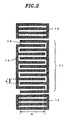
- Each surface acoustic wave resonator includes an IDT electrode 11 and reflectors 12 as shown in Fig. 2 .
- the IDT electrode 11 is formed of two comb-like electrodes that face and engage each other, each electrode being composed of electrode fingers 13 and a bus bar (common electrode) 14.
- the electrode-finger pitch of the IDT electrode 11 is defined as the distance p from the middle of the electrode-finger in the width direction to the middle of the adjacent electrode finger in the width direction as shown Fig. 2 .
- the crossing width w is defined as the width of the region where the electrode fingers of the comb-like electrodes are overlapping.
- an additional surface acoustic wave resonator 15a for adding a capacitance component is connected in parallel with the series-arm surface acoustic wave resonator 7b.
- Optimal connection between the series-arm surface acoustic wave resonators 7a to 7d and the additional surface acoustic wave resonator 15a is determined by the frequency design of the series-arm surface acoustic wave resonators 7a to 7d forming the passband. Therefore, connection of the additional surface acoustic wave resonator 15a to the series-arm surface acoustic wave resonators 7a to 7d is not necessarily specified.
- an additional surface acoustic wave resonator 15a which is relatively small, is added to the series-arm surface acoustic wave resonator 7a to which the maximum power is applied, it may be affected by heat from the series-arm surface acoustic wave resonator 7a.
- Fig. 3 shows the pass characteristics of the duplexer 20.
- the horizontal axis represents the frequency and the vertical axis represents the attenuation amount.
- the characteristic curve 16a indicated by the solid line shows the pass-band characteristics of the first surface acoustic wave filter 1
- the characteristic curve 16b indicated by the solid line shows the pass characteristics of the second surface acoustic wave filter 2.
- the characteristic curve 17a indicated by the dashed line shows the pass characteristics of the transmission filter of the duplexer of the comparative example A
- the characteristic curve 17b indicated by the dashed line shows the pass-band characteristics of the reception filter of the comparative example A.
- the duplexer of the comparative example A has the same configuration as that of the present embodiment except that a capacitor (condenser) with the same electrostatic capacitance as that of the additional surface acoustic wave resonator 15a is used instead of the additional surface acoustic wave resonator 15a.
- the characteristic curve 18a indicated by the dotted line shows the pass characteristics of the transmission filter of the duplexer of the comparative example B
- the characteristic curve 18b indicated by the dotted line shows the pass characteristics of the reception filter of the comparative example B.
- the duplexer of the comparative example B has the same configuration as that of the present embodiment except that there is no additional surface acoustic wave resonator 15a.
- the shoulder characteristics of the first surface acoustic wave filter 1 of the present embodiment and of the transmission filter of the comparative example A are much steeper than those of the transmission filter of the comparative example B.
- the attenuation amount of the comparative example A is worse than that of the comparative example B.
- the additional surface acoustic wave resonator 15a of the present embodiment is used as a capacitance. Due to its resonance characteristics, for example, the attenuation amount at frequencies from 898 MHz to 901 MHz can be improved by 7.3 dB compared to the comparative example A. Furthermore, the attenuation amount at 925 MHz can be enhanced by about 1.7 dB.
- the local maximum point 19a corresponds to the resonance frequency of the additional surface acoustic wave resonator 15a and the local minimum point 19b corresponds to the anti-resonance frequency thereof.
- An attenuation pole is locally formed by the local minimum point 19b.
- a frequency difference between a resonance frequency and an anti-resonance frequency is almost determined by a material constant of the piezoelectric substrate used.
- the capacitance connected in parallel as in the present embodiment the resonance frequency is not changed but the anti-resonance frequency is lowered. The same effect applies to the additional surface acoustic wave resonator 15a used in the present embodiment.
- the anti-resonance frequency of the series-arm surface acoustic wave resonator 7b is lowered by the capacitance of the additional surface acoustic wave resonator 15a connected in parallel so that the steep shoulder characteristics of the filter can be achieved.
- the anti-resonance frequency of the additional surface acoustic wave resonator 15a is lowered by the capacitance of the series-arm surface acoustic wave resonator 7b connected in parallel. Therefore, this should be considered to locate an attenuation pole at a desirable frequency.
- Fig. 4 is a surface acoustic wave device in accordance with the second embodiment of the present invention.
- Additional surface acoustic wave resonator 15a with a larger capacitance is preferable to make further the shoulder characteristics near the passband steeper.
- additional surface acoustic wave resonators (15a and 15b in the example illustrated in Fig. 4 ) are preferably connected to several series-arm surface acoustic wave resonators, e.g., 7b and 7d.
- the dashed line indicates the characteristic curve 16c when the additional surface acoustic wave resonator 15a of Fig. 1 has a capacitance of about 3.4 pF.
- the shoulder characteristics near the passband are steep.
- a surface acoustic wave resonator with the same configuration and a capacitance of about 1.7 pF is used as the additional surface acoustic wave resonators 15a and 15b, there occurs no ripple 19c and the steep shoulder characteristics are steeper.
- the capacitance of the additional surface acoustic wave resonator 15a of Fig. 1 for suppressing the ripple near the passband is preferably not higher than about 20% of those of the series-arm surface acoustic wave resonators 7b and 7d of Fig. 4 to which the additional surface acoustic wave resonators 15a and 15b are respectively added.
- the resonators shown in the drawings refer to the surface acoustic wave resonators.
- a surface acoustic wave device includes the same elements as that shown in Fig. 4 except that the additional surface acoustic wave resonators 15a and 15b have different electrode-finger pitches while having substantially the same capacitance.
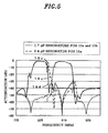
- the characteristic curve 16e indicated by the dashed line shows the pass characteristics when the additional surface acoustic wave resonators 15a and 15b have the same configuration.
- the solid line indicates the characteristic curve 16f when the electrode-finger pitch of the IDT electrode of the additional surface acoustic wave resonator 15b is modified so that its resonance frequency is increased by 7 MHz while its capacitance is maintained the same as that of the additional surface acoustic wave resonator 15a. In this manner, higher attenuation amount at higher frequencies can be obtained in comparison with the case of the additional surface acoustic wave resonators 15a and 15b with the exact same configuration.
- the surface acoustic save device of the fourth embodiment has a configuration same as that shown in Fig. 4 , except that the resonance frequencies of the additional surface acoustic wave resonators 15a and 15b are higher.
- the characteristics curve 16h indicated by the solid line represents the pass characteristics.
- the resonance frequency of the additional surface acoustic wave resonator 15b is 7 MHz lower than that of the additional surface acoustic wave resonator 15a while the additional surface acoustic wave resonator 15b has substantially the same capacitance as that of the additional surface acoustic wave resonator 15a.
- the resonance frequency of the additional surface acoustic wave resonator 15b is located within the passband of the second surface acoustic wave filter 2.
- the characteristics curve 16g indicated by the dashed line shows the pass characteristics when the additional surface acoustic wave resonators 15a and 15b have the same configuration and their resonance frequency is located outside the passband of the second surface acoustic wave filter 2.
- the additional surface acoustic wave resonator 15b whose resonance frequency is located within the passband of the second surface acoustic wave filter 2 generates a significant ripple 19d within the passband of the second surface acoustic wave filter 2.
- the resonance frequency of the additional surface acoustic wave resonator 15b needs to be higher than frequencies of the passband of the second surface acoustic wave filter 2.
- the electrode-finger pitch of the IDT electrode of the additional surface acoustic wave resonator 15b is preferably smaller than that of the surface acoustic wave resonator with the highest resonance frequency among the series-arm surface acoustic wave resonators 9b, 9c and 9d of the second surface acoustic wave filter 2.
- the series-arm surface acoustic wave resonator 9a of the second surface acoustic wave filter 2 is not included herein.
- the series-arm surface acoustic wave resonator 9a may be intentionally made to have the resonance frequency rather higher than those of the other series-arm surface acoustic wave resonators and, in this case, the series-arm surface acoustic wave resonator 9a does not contribute to the formation of the passband of the second surface acoustic wave filter 2.
- the electrode-finger pitch of the IDT electrode of the additional surface acoustic wave resonator 15b is set 0.5 to 0.98 times the electrode-finger pitch of the IDT electrodes of the series-arm surface acoustic wave resonators 9b, 9c and 9d of the second surface acoustic wave filter 2. If less than 0.5 times, excitation efficiency of the IDT electrode becomes poor and therefore the anti-resonance resistance for an effective attenuation pole cannot be obtained. If more than 0.98 times, the passband of the second surface acoustic wave filter 2 is deteriorated.
- the configuration of the surface acoustic wave device of the fifth embodiment is same as that shown in Fig. 1 , except that the ratio w/p in the IDT electrode of the additional surface acoustic wave resonator 15a is higher than that of the series-arm surface acoustic wave resonator 7b to which the additional surface acoustic wave resonator 15a is connected in parallel.
- the distance between electrode fingers of the additional surface acoustic wave resonator 15a is reduced, thereby increasing the capacitance. Therefore, the capacitance for the desirable shoulder characteristics can be obtained by the smaller area.
- the occupation area of the first surface acoustic wave filter 1 is smaller, whereby the surface acoustic wave device can be miniaturized and productivity of the piezoelectric substrate which produces a number of the first surface acoustic wave filters 1 can be improved.
- the configuration of the surface acoustic wave device of the sixth embodiment is same as that shown in Fig. 1 , except that the ratio w/p in the IDT electrode of the additional surface acoustic wave resonator 15a is lower than that of the series-arm surface acoustic wave resonator 7b to which the additional surface acoustic wave resonator 15a is connected in parallel.
- the resonance and anti-resonance resistance of the additional surface acoustic wave resonator 15a increases. Accordingly, the attenuation amount of the local maximum point (resonance point) and the local minimum point (anti-resonance point) can be further increased.
- the duplexers of the embodiments have the steep shoulder characteristics of the filter characteristics and the excellent out-of-band attenuation characteristics near the passband. Further, the duplexers of the embodiments can be applied to communication devices.
- the communication device of the present embodiment which includes a duplexer having the surface acoustic wave device of the present embodiment, is provided with a mixer for generating an antenna transmission signal by mixing a transmission signal with a carrier signal, a band-pass filter with a surface acoustic wave device for attenuating unwanted signals from the antenna transmission signal and a power amplifier for amplifying the antenna transmission signal and transmitting the amplified antenna transmission signal to the antenna via a duplexer.
- the communication device of the present embodiment which includes a duplexer having the surface acoustic wave device of the present embodiment, is also provided with the antenna, a low-noise amplifier for amplifying the antenna reception signal received by the antenna through the duplexer, a band-pass filter with a surface acoustic wave device for attenuating unwanted signals from the antenna reception signal amplified by the low-noise amplifier and a mixer for separating a reception signal from the carrier signal of the antenna reception signal transmitted from the band-pass filter.
- Fig. 8 is a block diagram schematically showing a configuration of an exemplary communication device 100.
- the communication device 100 mainly includes a transmission/reception unit 300, an antenna 400, a controller 200, an operating unit 600, a microphone MP and a speaker SP.
- the controller 200 collectively controls various operations of the communication device 100.
- the controller 200 is provided with a CPU, a RAM, a ROM and the like, and it reads and executes programs stored in the ROM so that various controls and functions of the communication device 100 can be made.
- An analog voice signal inputted into the transmission/reception unit 300 from the microphone MP through the controller 200 is converted from an analog signal to a digital signal by a DSP (Digital Signal Processor) 301, modulated by a modulator 302 and then frequency-converted by a mixer 303 using an oscillation signal created by a local oscillator 320.
- the output of the mixer 303 sequentially passes through a transmissionband-pass filter 304, a power amplifier 305 and a duplexer 306 and it is then outputted from the antenna 400 as a transmission signal.
- a received signal is fed to a mixer 309 from the antenna 400 through the duplexer 306, a low-noise amplifier 307 and a reception band-pass filter 308.
- the mixer 309 frequency-converts the received signal using the oscillation signal created by the local oscillator 320, the converted signal passes through a low-pass filter 310 and is then demodulated by a demodulator 311. Further, the demodulated signal is converted from a digital signal into an analog signal by the DSP 301 and the converted signal, i.e. the analog voice signal, is outputted from the speaker SP after passing through the controller 200.
- the operating unit 600 receives various inputs for the communication device 100 from users and is composed of, e.g., a variety of buttons.
- duplexers of the embodiments are used as the duplexer 306 of the communication device 100.
- ladder filters have been exemplified for the second surface acoustic wave filter 2 in the above described embodiments, it should be noted that the second surface acoustic wave filter 2 is not necessarily of a ladder-type and DMS-type or lattice-type filters can be used.
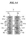
- Fig. 14 is a plan view for schematically showing a typical structure of a DMS (Double Mode Saw) filter D included in a duplexer.
- the DMS filter D which is a multi-mode filter, includes a filter Da and another filter Db connected to each other in a two-stage structure.
- the filter Da includes three IDTs 41a, 41b and 41c adjacent to each other; and two reflectors 42 respectively arranged at both ends of an IDT electrode group having the three IDTs 41a, 41b and 41c.
- the structure of the DMS filter D is not limited to the two-stage structure.
- Each of the IDTs 41a, 41b and 41c includes a pair of comb-shaped electrodes arranged to face each other such that the lengthwise direction thereof is perpendicular to the propagation direction of the surface acoustic wave in the piezoelectric substrate.
- Each of the reflectors 42 also includes lattice-shaped electrodes arranged such that the lengthwise direction thereof is perpendicular to the propagation direction of the surface acoustic wave in the piezoelectric substrate.
- the filter Db includes three IDTs 41d, 41e and 41f adjacent to each other; and two reflectors 42 respectively arranged at both ends of an IDT array having the three IDTs 41a, 41b and 41c.
- Each of the IDTs 41d, 41e and 41f includes a pair of comb-shaped electrodes arranged to face each other such that the lengthwise direction thereof is perpendicular to the propagation direction of the surface acoustic wave in the piezoelectric substrate.
- Each of the reflectors 42 also includes lattice-shaped electrodes arranged such that the lengthwise direction thereof is perpendicular to the propagation direction of the surface acoustic wave in the piezoelectric substrate.
- the configuration of the DMS filter D is not limited to the above one in which the filter of each stage in the DMS filter D includes three IDTs, but any configuration may be adopted so long as it includes two or more IDTs.
- the multi-mode filter as the second surface acoustic wave filter 2 as above, there is an advantage in that steeper characteristics can be achieved in frequencies lower than the reception passband when the reception signal is received. Further, the number of electrode pairs, the crossing width, the number of reflectors and the like can be properly chosen according to the design.
- a piezoelectric substrate was formed of lithium tantalite (LiTaO 3 ), and a Ti thin-film with a thickness of 6 nm was formed on a main surface of the substrate. Then, an Al-Cu thin-film with a thickness of 125 nm was formed thereon. The Ti and Al-Cu thin-films were laminated three times alternately, thereby forming a Ti/Al-Cu laminated film having six thin-layers in total.
- the Al-Cu thin-film refers to an alloy thin-film where a very small amount of Cu was added to Al.
- a photoresist with a thickness of about 0.5 ⁇ m was coated on the main surface of the phizoelectric substrate by using a resist coater. Thereafter, photoresist patterns were exposed by a reduction projection aligner (stepper) so that surface acoustic wave resonators, wiring and electrodes were arranged as shown in Fig. 9 . After that, an undesired photoresist was dissolved by a development apparatus with using an alkaline developing solution.
- an electrode pattern shown in Fig. 9 was formed by an RIE (Reactive Ion Etching) apparatus.
- the reference numeral 1' indicates a transmission filter unit and the reference numeral 2' indicates a reception filter unit.
- the circuit configuration of the surface acoustic wave resonator determining the passband was the same as that of Fig. 1 and additional surface acoustic wave resonators 15a, 15b and 15c serving as capacitance elements were respectively connected in parallel with series-arm surface acoustic wave resonators 7b, 7d and 9d.
- a protective film (not shown) was then formed on a predetermined area of the circuit pattern. That is, a SiO 2 film with a thickness of about 15 nm was formed on the main surface of the electrode pattern and piezoelectric substrate by using a CVD (Chemical Vapor Deposition) apparatus. After then, the photoresist was patterned by photolithography and the SiO 2 film of electrodes of the flip-chip, e.g., input/output electrodes, ground electrodes and pad electrodes, was etched by the RIE apparatus or the like.
- CVD Chemical Vapor Deposition
- the electrode had 0.01 ⁇ m of Cr, 1 ⁇ m of Ni and 0.2 ⁇ m of Au.
- the photoresist and the undesired laminated electrode portion were simultaneously removed by a lift-off method, and the part where the laminated electrode had been formed, i.e. an input electrode 21 of the transmission filter, an output electrode 22 of the transmission filter, an input electrode 23 of the reception filter, an output electrode 24 of the reception filter, a ground electrode 25 of the transmission filter and a ring-shape electrode 26, became the electrode unit of the flip-chip to connect a bump of the flip-chip. Further, the ring-shape electrode 26 was to airtightly seal the filter units as will be described later, and it can be formed if necessary. Here, the ring-shape electrode 26 also serves as a ground electrode of the reception filter unit 2'.
- the piezoelectric substrate was diced along the dicing line and then separated into filter chips 50.
- a conductive member 32 was printed on a conductor which was made of silver and formed on a ceramic circuit board 28 of a laminated structure corresponding to the input electrode 21 of the transmission filter, the output electrode 22 of the transmission filter, the input electrode 23 of the reception filter, the output electrode 24 of the reception filter, the ground electrode 25 of the transmission filter and the ring-shape electrode 26.
- a solder was used as the conductive member 32.
- the circuit board 28 was a board for a multiple molding.
- each chip 50 was provisionally joined to the ceramic circuit board 28 by a flip-chip mounting device such that a surface where the electrodes were formed faced down, which was performed in N 2 atmosphere.
- bake was performed in N 2 atmosphere to melt the solder of the conductive member 32, thereby joining the chips 50 and the circuit board 28 together.
- an inductor formed of a line (not shown) which connected the signal potential to the ground potential inside the circuit board 28 realized the matching circuit 6.
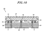
- Fig. 10 shows a cross-sectional view of the duplexer 20.
- Fig. 9 shows a plan view of the piezoelectric substrate 27 facing the ceramic circuit board 28 in Fig. 10
- Fig. 10 is a cross sectional view of the piezoelectric substrate 27 taken along a line A-A of Fig. 9 .
- each piece of the circuit board 28 has an area of 2.5 x 2.0 mm square and a thickness of 0.375 mm.
- Fig. 11 is a graph showing the pass-band characteristics of the duplexers A and B.
- the horizontal axis represents the frequency (unit: MHz) and the vertical axis represents the attenuation amount (unit: dB).
- the characteristic curve 16i indicated by the solid line shows the pass-band characteristics of the duplexer A of the present example, while the characteristic curve 18c indicated by the dashed line shows the pass-band characteristics of the duplexer B of the comparative example 1.
- the characteristic curve 17c indicated by the dotted line showing the pass-band characteristics of the duplexer C as the comparative example 2 where the additional surface acoustic wave resonators 15a, 15b and 15c are replaced by capacitors with the same capacitance was derived from simulation.
- the local maximum point 19e and the local minimum point 19f respectively coincide with the resonance frequency and anti-resonance frequency of the additional surface acoustic wave resonators 15a and 15b.
- the electrode-finger pitch of each IDT electrode of the additional surface acoustic wave resonators 15a and 15b was adjusted so that the resonance and anti-resonance frequencies of the additional surface acoustic wave resonators 15a and 15b could substantially coincide with each other.
- the electrode-finger pitch thereof was about 2.39 ⁇ m
- the number of the pairs of electrode fingers was 100
- the electrode-finger crossing width was about 76 ⁇ m.
- the electrode-finger pitch thereof was about 2.39 ⁇ m
- the number of the pairs of electrode fingers was 80
- the electrode-finger crossing width was about 86 ⁇ m.
- the additional surface acoustic wave resonators 15a and 15b had an electrode-finger pitch of about 2.14 ⁇ m, the number of the pairs of electrode fingers was 20 and an electrode-finger crossing width of about 86 ⁇ m.
- the resonance frequency and anti-resonance frequency of the surface acoustic wave resonator 15c correspond to the local maximum point 19g and the local minimum point 19h, respectively.
- the electrode-finger pitch thereof was about 2.23 ⁇ m
- the number of the pairs of electrode fingers was 80
- the electrode-finger crossing width was about 22 ⁇ m.
- the surface acoustic wave resonator 15c had an electrode-finger pitch of about 2.02 ⁇ m, the number of the pairs of electrode fingers was 10 and an electrode-finger crossing width of about 80 ⁇ m.
- the ratio w/p in the IDT electrode of the surface acoustic wave resonator determining the passband was about 0.43, while the ratio w/p in the IDT electrode of the additional surface acoustic wave resonators 15a, 15b and 15c serving as capacitance components was about 0.63.
- the additional surface acoustic wave resonators 15a and 15b had a capacitance of 1.7 pF and the surface acoustic wave resonator 15c had a capacitance of 0.5 pF.
- the shoulder characteristics near the passbands of the transmission and reception filters 1 and 2 of the duplexer A of the present example were much steeper than those of the comparative example 1.
- the attenuation amount of the duplexer A at frequencies from 898 MHz to 901 MHz was improved by about 19.9 dB compared to the duplexer C of the comparative example 2.
- the attenuation amount at 925 MHz was also improved by approximately 4.9 dB.
- the attenuation amount of the duplexer A at frequencies from 843 MHz to 846 MHz was improved by about 24.9 dB compared to the duplexer B of the comparative example 1.
- the present invention is not limited to the embodiments and examples described above and various modification may be made without departing from the scope of the invention.
- at least one of the additional surface acoustic wave resonators 15a, 15b and 15c serving as capacitance components may be used and more surface acoustic wave resonators may also be used.
- the additional surface acoustic wave resonators 15a, 15b and 15c serving as capacitance components may have different electrode-finger pitches or the ratio w/p values. If so, attenuation poles may be located at different many locations. In particular, in the same filter, by placing the anti-resonance frequencies of the additional surface acoustic wave resonators 15a, 15b and 15c serving as capacitance components close to each other, the attenuation amount may be increased in the wide band. If the anti-resonance frequencies are the same, the attenuation amount may be further increased.
- partial omission or apodization may be performed on the structure of the additional surface acoustic wave resonators 15a, 15b and 15c serving as capacitance components and the capacitances or anti-resonance frequencies thereof may be adjusted. This is the same to the surface acoustic wave resonators forming the passband.
- the present invention may also be applied to surface acoustic wave devices with transmission filters according to different standards.
Landscapes
- Physics & Mathematics (AREA)
- Acoustics & Sound (AREA)
- Surface Acoustic Wave Elements And Circuit Networks Thereof (AREA)
Abstract
Description
- The present invention relates to a surface acoustic wave device, and a duplexer and a communication device using same and particularly to a surface acoustic wave device, and a duplexer and a communication device using same with steeper shoulder characteristics near a passband, which has an attenuation pole at frequencies higher than those of the passband.
- Recently, with the development of electrode materials and electrode structures having high power durability, surface acoustic wave filters have become necessary for duplexers that serve to separate transmission signals from reception signals in mobile communication devices.
- The duplexers need to separate signals of a transmission band sufficiently from signals of a reception band close to the signals of the transmission band. For example, if a transmission band is at frequencies lower than a reception band, the duplexers need to have steep shoulder characteristics at a high frequency region of the transmission band. A circuit structure with a ladder filter with excellent power durability is generally used in a transmission filter passing signals amplified by a power amplifier.
- Further, a technique for adding a capacitance in parallel with a resonator of a ladder filter is known to obtain steep shoulder characteristics of the ladder filter.
- The recent trend toward modification of the communication standards and global roaming of mobile phones has prompted the requirement to attenuate strictly the frequency bands that are used as another standard near the passbands of duplexers.
- The present invention has been conceived to meet the requirement described above, and provides a surface acoustic wave device, and a duplexer and a communication device using the same with steeper shoulder characteristics of a passband and with an attenuation pole at frequencies higher than the frequencies of the passband.
- According to an aspect of the present invention, a surface acoustic wave device includes a first surface acoustic wave filter and a second surface acoustic wave filter. The second surface acoustic wave filter has a passband at frequency range higher than that of the first surface acoustic wave filter. The first surface acoustic wave filter forms a ladder filter circuit, and includes a series-arm surface acoustic wave resonator, a parallel-arm surface acoustic wave resonator and an additional surface acoustic wave resonator. The series-arm surface acoustic wave resonator includes an IDT electrode and is on a series arm of the ladder filter circuit. The parallel-arm surface acoustic wave resonator includes an IDT electrode and is on a parallel arm of the ladder filter circuit. The additional surface acoustic wave resonator includes an IDT electrode, is connected in parallel with the series-arm surface acoustic wave resonator and has a resonance frequency which is higher than the frequency range of the passband of the second surface acoustic wave filter. Further, "a second surface acoustic wave filter whose passband is at frequencies higher than a passband of the first surface acoustic wave filter" is a surface acoustic wave resonator whose resonant frequency is higher than the highest frequency in the passband of the second surface acoustic wave filter.
- Further, it is preferable that an electrode-finger pitch of the IDT electrode of the additional surface acoustic wave resonator is smaller than that of the series-arm surface acoustic wave resonator to which the additional surface acoustic wave resonator is connected in parallel.
- Further, it is preferable that the electrode-finger pitch of the IDT electrode of the additional surface acoustic wave resonator is set 0.5 to 0.95 times that of the series-arm surface acoustic wave resonator to which the additional surface acoustic wave resonator is connected in parallel.
- Further, it is preferable that the second surface acoustic wave filter forms a ladder filter circuit which includes a series-arm surface acoustic wave resonator with an IDT electrode which is connected to a series arm of the ladder filter circuit, and a parallel-arm surface acoustic wave resonator with an IDT electrode which is connected to a parallel arm of the ladder filter circuit, wherein the electrode-finger pitch of the IDT electrode of the additional surface acoustic wave resonator is smaller than that of the series-arm surface acoustic wave resonator of the second surface acoustic wave filter.
- Further, it is preferable that the electrode-finger pitch of the IDT electrode of the additional surface acoustic wave resonator is set 0.5 to 0.98 times that of the series-arm surface acoustic wave resonator of the second surface acoustic wave filter.
- Further, it is preferable that a value of (electrode-finger width)/(electrode-finger pitch) of the IDT electrode of the additional surface acoustic wave resonator is higher than that of the series-arm surface acoustic wave resonator to which the additional surface acoustic wave resonator is connected in parallel.
- Further, it is preferable that the (electrode-finger width)/(electrode-finger pitch) of the IDT electrode of the surface acoustic wave resonator is lower than that of the series-arm surface acoustic wave resonator to which the surface acoustic wave resonator is connected in parallel.
- According to another aspect of the present invention, a duplexer includes the surface acoustic wave device of the above. The duplexer also includes an input terminal of the first surface acoustic wave filter, an output terminal of the second surface acoustic wave filter and a connecting portion.
- According to further aspect of the present invention, a communication device includes the above-mentioned duplexer, an antenna, a mixer and a power amplifier. The mixer mixes a transmission signal with a carrier signal and outputs the antenna transmission signal. The power amplifier amplifies the antenna transmission signal and outputs the amplified antenna transmission signal to the antenna via the duplexer.
- According to further another aspect of the present invention, a communication device includes a duplexer, an antenna, a amplifier and a mixer. The duplexer includes the surface acoustic wave device of the above. The duplexer includes the above-mentioned surface acoustic wave. The antenna outputs an antenna reception signal to the duplexer. The amplifier amplifies the antenna reception signal received from the duplexer. The mixer separates the reception signal from a carrier signal of the amplified antenna reception signal received from the amplifier.
- The present invention will become apparent from the following detailed description in conjunction with the accompanying drawings, in which:
-
Fig. 1 is a circuit diagram of a surface acoustic wave device according to the first embodiment of the present invention; -
Fig. 2 is a plan view of a surface acoustic wave resonator; -
Fig. 3 shows the pass characteristics of the surface acoustic wave device shown inFig. 1 according to the first embodiment of the present invention; -
Fig. 4 is a circuit diagram of a surface acoustic wave device accord to the second embodiment of the present invention; -
Fig. 5 shows the pass characteristics of the surface acoustic wave device shown inFig. 4 according to the second embodiment of the present invention; -
Fig. 6 shows the pass characteristics of a surface acoustic wave device according to the third embodiment of the present invention; -
Fig. 7 illustrates the preferable scope of the electrode-finger pitch of an additional surface acoustic wave resonator for adding a capacitance component in the surface acoustic wave device according to the fouth embodiment of the present invention; -
Fig. 8 is a block diagram of a communication device using the surface acoustic wave device according to the present embodiment; -
Fig. 9 is a plan view of a piezoelectric substrate of the surface acoustic wave device according to the present embodiment; -
Fig. 10 is a cross-sectional view of an exemplary surface acoustic wave device of the present embodiment; -
Fig. 11 is shows the pass characteristics of the exemplary surface acoustic wave device of the present embodiment;Fig. 12 is a circuit diagram of the conventional surface acoustic wave device; -
Figs. 13A and13B show the pass characteristics of the conventional surface acoustic wave device; and -
Fig. 14 is a plan view of a DMS filter used for the reception filter in the surface acoustic wave device according to the embodiment. - Hereinafter, embodiments of the present invention is described below with reference to the accompanying drawings. Herein, the same reference numerals are given to the same parts in the drawings. Further, the size of electrode fingers of each surface acoustic wave resonator, the distance between the electrode fingers or the number of the electrode fingers is chosen for illustration purpose only and is not limited to the size, the distance or the number in the drawings respectively.
- In the surface acoustic wave device of the embodiment, the additional surface acoustic wave resonator (hereinafter, referred to as also an "additional surface acoustic wave resonator for adding a capacitance component") with an IDT electrode is connected in parallel to the series-arm surface acoustic wave resonator of the first surface acoustic wave filter constituting the ladder filter circuit. The surface acoustic wave resonator with the IDT electrode functions as a capacitance at frequencies other than the resonance frequency so that the steep shoulder characteristics near a high frequency region of the passband can be obtained. To improve further the shoulder characteristics, a larger capacitance can be connected in parallel to the series-arm surface acoustic wave resonator. However, in this case, the out-of-band attenuation characteristics are deteriorated. This situation is described as follows with reference to
Figs. 12 ,13A and13B . -
Fig. 12 is a circuit diagram of a knownladder filter 60.Figs. 13A and13B are graphs showing the pass characteristics of theladder filter 60 ofFig. 12 ;Fig. 13A is a graph showing the pass characteristics of the passband in a specified narrow frequency range andFig. 13B is a graph showing the pass characteristics over a broad frequency range including high frequencies. - Referring to
Fig. 12 , theladder filter 60 is composed of series-arm surfaceacoustic wave resonators acoustic wave resonators acoustic wave resonators 62a to 62c are connected between signal potentials and the ground potential. Capacitances of the parallel-arm surfaceacoustic wave resonators 62a to 62c enter into resonance with inductances of the wires connecting them to the ground potential. It is well known that such a resonance results in an attenuation pole located at a frequency higher than the frequencies of the passband. In case of the example shown inFig. 12 , an attenuation pole is located at around 1.5 GHz by the parallel-arm surfaceacoustic wave resonators 62a and 62b, awire 64a, the parallel-arm surfaceacoustic wave resonator 62c and awire 64b. - Further, a
capacitance 63 can be added to the series-arm surfaceacoustic wave resonator 61b in parallel as shown inFig. 12 to obtain more steeper characteristics near the passband, which is described with reference toFig. 13A . InFig. 13A , the solid line shows the pass characteristics without thecapacitance 63, while the dotted line shows the pass characteristics with thecapacitance 63 of 2 pF. The addition of thecapacitance 63 improves the attenuation amount at 843 MHz by about 14 dB. However, the attenuation amount outside the passband is deteriorated by the addition of thecapacitance 63 as shown inFig. 13B . Therefore, the capacitance connected thereto for the steep shoulder characteristics is limited in order to achieve the desired attenuation amount outside the passband. Accordingly, in the present embodiment, to achieve the attenuation amount in the necessary frequency band as well as the steep shoulder characteristics of the filter with using a larger capacitance, an additional surface acoustic wave resonator with an IDT electrode is used as a capacitance. - If an additional surface acoustic wave resonator is newly connected in parallel with the series-arm surface acoustic wave resonator, it is possible to locate a local attenuation pole at the anti-resonance frequency of the additional surface acoustic wave resonator
- In the present embodiment, the resonance frequency of the additional surface acoustic wave resonator newly connected to the series-arm surface acoustic wave resonator forming the passband of the first surface acoustic wave filter is higher than the frequencies of the passband of the second surface acoustic wave filter which are higher than those of the passband of the first surface acoustic wave filter. By this, when the first and second surface acoustic wave filters are connected to each other, the resonance characteristics of the additional surface acoustic wave resonator newly connected do not deteriorate the pass characteristics of the second surface acoustic wave filter.
- Therefore, according to the present invention, a surface acoustic wave device can have an attenuation pole located around the high frequency side of the passband as well as the steep shoulder characteristics.
- To obtain the attenuation pole around the high frequency side of the passband, it is preferable that the electrode-finger pitch of the IDT electrode of the additional surface acoustic wave resonator is smaller than that of the series-arm surface acoustic wave resonator to which the additional surface acoustic wave resonator is connected in parallel.
- More preferably, the electrode-finger pitch of the IDT electrode of the surface acoustic wave resonator is set 0.5 to 0.95 times that of the series-arm surface acoustic wave resonator to which the additional surface acoustic wave resonator is connected in parallel. Within this range, a reduction of excitation efficiency of acoustic waves of the additional surface acoustic wave resonator newly connected is suppressed and a deterioration of the anti-resonance resistance is suppressed, and therefore an effective attenuation pole can be obtained. Further, insertion losses in the passband of the first surface acoustic wave filter become smaller.
- Further, in case that the second surface wave filter is also of a ladder-type, the electrode-finger pitch of the IDT electrode of the additional surface acoustic wave resonator which is connected in parallel to the series-arm surface acoustic wave resonator of the first surface acoustic wave filter is preferably smaller than the electrode-finger pitch of the series-arm surface acoustic wave resonator of the second surface acoustic wave filter.
- More preferably, the electrode-finger pitch of the IDT electrode of the additional surface acoustic wave resonator is set 0.5 to 0.98 times that of the series-arm surface acoustic wave resonator of the second surface acoustic wave filter. Within this range, a reduction of excitation efficiency of acoustic waves of the additional surface acoustic wave resonator newly connected is suppressed and a deterioration of the anti-resonance resistance is suppressed, and therefore an effective attenuation pole can be obtained. Further, a deterioration in the passband of the second surface acoustic wave filter is suppressed.
- If the additional surface acoustic wave resonator for adding a capacitance component other than the surface acoustic wave resonators forming the passband is newly added, an area of the surface acoustic wave device is increased. Therefore, the newly connected additional surface acoustic wave resonator should be small as much as possible. Further, in case that, in accordance with the present embodiment, a ratio (ratio w/p) of the electrode-finger width to the electro de-finger pitch in the IDT electrode of the additional surface acoustic wave resonator is higher than that of the series-arm surface acoustic wave resonator to which the additional surface acoustic wave resonator is connected in parallel, the desired capacitance can be realized with a smaller number of the pairs of electrode-fingers and a smaller crossing width.
- On the contrary, in case that the ratio w/p in the IDT electrode of the additional surface acoustic wave resonator is lower than that of the series-arm surface acoustic wave resonator to which the additional surface acoustic wave resonator is connected in parallel, the resonance resistance and the anti-resonance resistance become large, and therefore the attenuation amount of the newly formed attenuation pole can be increased.
- According to the present invention, a duplexer, which uses the surface acoustic wave device of the present invention, can have steeper shoulder characteristics of the filter characteristics and the excellent out-of-band attenuation characteristics around the passband, resulting in the preferable electrical characteristics.
- According to the present invention, a communication device can achieve a communication performance in which the currently used communication standard is less interfered with other near communication standards.
-
Fig. 1 illustrates a surface acoustic wave device in accordance with the first embodiment of the present invention. -
Fig. 1 shows aduplexer 20 includes the first surfaceacoustic wave filter 1 serving as a transmission filter and the second surfaceacoustic wave filter 2 serving as a reception filter. A transmission signal from a transmission circuit is inputted to the first surfaceacoustic wave filter 1 through aterminal 3 and then transmitted to a terminal 4 coupled to an antenna (not shown). A signal received by the antenna is inputted to the surfaceacoustic wave filter 2 through the terminal 4 and then transmitted to a reception circuit through aterminal 5. In this case, since the output terminal of the transmission filter and the input terminal of the reception filter are the same, theduplexer 20 is provided with amatching circuit 6 so each filter acts like a high impedance of the passband of the other filter. Thematching circuit 6 may be included in theduplexer 20 or provided separately. - In
Fig. 1 , the first surfaceacoustic wave filter 1 is includes four series-arm surfaceacoustic wave resonators acoustic wave resonators filters acoustic wave filter 1 also includes an additional surfaceacoustic wave resonator 15a that is included in the circuit. The second surfaceacoustic wave filter 2 is configured with a circuit including four series-arm surfaceacoustic wave resonators acoustic wave resonators - Each surface acoustic wave resonator includes an
IDT electrode 11 and reflectors 12 as shown inFig. 2 . TheIDT electrode 11 is formed of two comb-like electrodes that face and engage each other, each electrode being composed of electrode fingers 13 and a bus bar (common electrode) 14. In this embodiment, the electrode-finger pitch of theIDT electrode 11 is defined as the distance p from the middle of the electrode-finger in the width direction to the middle of the adjacent electrode finger in the width direction as shownFig. 2 . Further, the crossing width w is defined as the width of the region where the electrode fingers of the comb-like electrodes are overlapping. - Further, an additional surface
acoustic wave resonator 15a for adding a capacitance component is connected in parallel with the series-arm surfaceacoustic wave resonator 7b. - Optimal connection between the series-arm surface
acoustic wave resonators 7a to 7d and the additional surfaceacoustic wave resonator 15a is determined by the frequency design of the series-arm surfaceacoustic wave resonators 7a to 7d forming the passband. Therefore, connection of the additional surfaceacoustic wave resonator 15a to the series-arm surfaceacoustic wave resonators 7a to 7d is not necessarily specified. However, if an additional surfaceacoustic wave resonator 15a, which is relatively small, is added to the series-arm surfaceacoustic wave resonator 7a to which the maximum power is applied, it may be affected by heat from the series-arm surfaceacoustic wave resonator 7a. Thus, it is preferable to add the additional surfaceacoustic wave resonator 15a to the series-arm surfaceacoustic wave resonator -
Fig. 3 shows the pass characteristics of theduplexer 20. InFig. 3 , the horizontal axis represents the frequency and the vertical axis represents the attenuation amount. The characteristic curve 16a indicated by the solid line shows the pass-band characteristics of the first surfaceacoustic wave filter 1, whereas the characteristic curve 16b indicated by the solid line shows the pass characteristics of the second surfaceacoustic wave filter 2. - The characteristic curve 17a indicated by the dashed line shows the pass characteristics of the transmission filter of the duplexer of the comparative example A, whereas the characteristic curve 17b indicated by the dashed line shows the pass-band characteristics of the reception filter of the comparative example A. Here, the duplexer of the comparative example A has the same configuration as that of the present embodiment except that a capacitor (condenser) with the same electrostatic capacitance as that of the additional surface
acoustic wave resonator 15a is used instead of the additional surfaceacoustic wave resonator 15a. - Furthermore, the characteristic curve 18a indicated by the dotted line shows the pass characteristics of the transmission filter of the duplexer of the comparative example B, whereas the characteristic curve 18b indicated by the dotted line shows the pass characteristics of the reception filter of the comparative example B. Here, the duplexer of the comparative example B has the same configuration as that of the present embodiment except that there is no additional surface
acoustic wave resonator 15a. - As shown in
Fig. 3 , the shoulder characteristics of the first surfaceacoustic wave filter 1 of the present embodiment and of the transmission filter of the comparative example A are much steeper than those of the transmission filter of the comparative example B. On the other hand, at frequencies higher than the frequencies of the passband of the second surfaceacoustic wave filter 2, the attenuation amount of the comparative example A is worse than that of the comparative example B. - Here, the additional surface
acoustic wave resonator 15a of the present embodiment is used as a capacitance. Due to its resonance characteristics, for example, the attenuation amount at frequencies from 898 MHz to 901 MHz can be improved by 7.3 dB compared to the comparative example A. Furthermore, the attenuation amount at 925 MHz can be enhanced by about 1.7 dB. - Further, in
Fig. 3 , the local maximum point 19a corresponds to the resonance frequency of the additional surfaceacoustic wave resonator 15a and the local minimum point 19b corresponds to the anti-resonance frequency thereof. An attenuation pole is locally formed by the local minimum point 19b. In general, a frequency difference between a resonance frequency and an anti-resonance frequency is almost determined by a material constant of the piezoelectric substrate used. However, by the capacitance connected in parallel as in the present embodiment, the resonance frequency is not changed but the anti-resonance frequency is lowered. The same effect applies to the additional surfaceacoustic wave resonator 15a used in the present embodiment. To be specific, the anti-resonance frequency of the series-arm surfaceacoustic wave resonator 7b is lowered by the capacitance of the additional surfaceacoustic wave resonator 15a connected in parallel so that the steep shoulder characteristics of the filter can be achieved. However, at the same time, the anti-resonance frequency of the additional surfaceacoustic wave resonator 15a is lowered by the capacitance of the series-arm surfaceacoustic wave resonator 7b connected in parallel. Therefore, this should be considered to locate an attenuation pole at a desirable frequency. -
Fig. 4 is a surface acoustic wave device in accordance with the second embodiment of the present invention. - An additional surface
acoustic wave resonator 15a with a larger capacitance is preferable to make further the shoulder characteristics near the passband steeper. And in order to avoid a ripple which occurs around the passband, as shown inFig. 4 , additional surface acoustic wave resonators (15a and 15b in the example illustrated inFig. 4 ) are preferably connected to several series-arm surface acoustic wave resonators, e.g., 7b and 7d. - In
Fig. 5 , the dashed line indicates the characteristic curve 16c when the additional surfaceacoustic wave resonator 15a ofFig. 1 has a capacitance of about 3.4 pF. The shoulder characteristics near the passband are steep. In contrast, inFig. 4 , when a surface acoustic wave resonator with the same configuration and a capacitance of about 1.7 pF is used as the additional surfaceacoustic wave resonators - Further, the capacitance of the additional surface
acoustic wave resonator 15a ofFig. 1 for suppressing the ripple near the passband is preferably not higher than about 20% of those of the series-arm surfaceacoustic wave resonators Fig. 4 to which the additional surfaceacoustic wave resonators - The resonators shown in the drawings refer to the surface acoustic wave resonators.
- According to the third embodiment of the present invention, a surface acoustic wave device includes the same elements as that shown in
Fig. 4 except that the additional surfaceacoustic wave resonators - In
Fig. 6 , the characteristic curve 16e indicated by the dashed line shows the pass characteristics when the additional surfaceacoustic wave resonators acoustic wave resonator 15b is modified so that its resonance frequency is increased by 7 MHz while its capacitance is maintained the same as that of the additional surfaceacoustic wave resonator 15a. In this manner, higher attenuation amount at higher frequencies can be obtained in comparison with the case of the additional surfaceacoustic wave resonators - The surface acoustic save device of the fourth embodiment has a configuration same as that shown in
Fig. 4 , except that the resonance frequencies of the additional surfaceacoustic wave resonators - In
Fig. 7 , the characteristics curve 16h indicated by the solid line represents the pass characteristics. Although the entire configuration in the present embodiment is the same as that shown inFig. 4 , the resonance frequency of the additional surfaceacoustic wave resonator 15b is 7 MHz lower than that of the additional surfaceacoustic wave resonator 15a while the additional surfaceacoustic wave resonator 15b has substantially the same capacitance as that of the additional surfaceacoustic wave resonator 15a. The resonance frequency of the additional surfaceacoustic wave resonator 15b is located within the passband of the second surfaceacoustic wave filter 2. In contrast, the characteristics curve 16g indicated by the dashed line shows the pass characteristics when the additional surfaceacoustic wave resonators acoustic wave filter 2. - As shown in the characteristic curve 16h indicated by the solid line, the additional surface
acoustic wave resonator 15b whose resonance frequency is located within the passband of the second surfaceacoustic wave filter 2 generates a significant ripple 19d within the passband of the second surfaceacoustic wave filter 2. In order to prevent the deterioration of the pass characteristics of the second surfaceacoustic wave filter 2, the resonance frequency of the additional surfaceacoustic wave resonator 15b needs to be higher than frequencies of the passband of the second surfaceacoustic wave filter 2. - To obtain the resonance frequency of the additional surface
acoustic wave resonator 15b higher than frequencies of the passband of the second surfaceacoustic wave filter 2, the electrode-finger pitch of the IDT electrode of the additional surfaceacoustic wave resonator 15b is preferably smaller than that of the surface acoustic wave resonator with the highest resonance frequency among the series-arm surfaceacoustic wave resonators acoustic wave filter 2. On the other hand, the series-arm surfaceacoustic wave resonator 9a of the second surfaceacoustic wave filter 2 is not included herein. This is because, in order to achieve desirable impedance matching with the first surfaceacoustic wave filter 1, the series-arm surfaceacoustic wave resonator 9a may be intentionally made to have the resonance frequency rather higher than those of the other series-arm surface acoustic wave resonators and, in this case, the series-arm surfaceacoustic wave resonator 9a does not contribute to the formation of the passband of the second surfaceacoustic wave filter 2. - More preferably, the electrode-finger pitch of the IDT electrode of the additional surface
acoustic wave resonator 15b is set 0.5 to 0.98 times the electrode-finger pitch of the IDT electrodes of the series-arm surfaceacoustic wave resonators acoustic wave filter 2. If less than 0.5 times, excitation efficiency of the IDT electrode becomes poor and therefore the anti-resonance resistance for an effective attenuation pole cannot be obtained. If more than 0.98 times, the passband of the second surfaceacoustic wave filter 2 is deteriorated. - The configuration of the surface acoustic wave device of the fifth embodiment is same as that shown in
Fig. 1 , except that the ratio w/p in the IDT electrode of the additional surfaceacoustic wave resonator 15a is higher than that of the series-arm surfaceacoustic wave resonator 7b to which the additional surfaceacoustic wave resonator 15a is connected in parallel. By doing this, the distance between electrode fingers of the additional surfaceacoustic wave resonator 15a is reduced, thereby increasing the capacitance. Therefore, the capacitance for the desirable shoulder characteristics can be obtained by the smaller area. Accordingly, the occupation area of the first surfaceacoustic wave filter 1 is smaller, whereby the surface acoustic wave device can be miniaturized and productivity of the piezoelectric substrate which produces a number of the first surfaceacoustic wave filters 1 can be improved. - The configuration of the surface acoustic wave device of the sixth embodiment is same as that shown in
Fig. 1 , except that the ratio w/p in the IDT electrode of the additional surfaceacoustic wave resonator 15a is lower than that of the series-arm surfaceacoustic wave resonator 7b to which the additional surfaceacoustic wave resonator 15a is connected in parallel. By doing so, the resonance and anti-resonance resistance of the additional surfaceacoustic wave resonator 15a increases. Accordingly, the attenuation amount of the local maximum point (resonance point) and the local minimum point (anti-resonance point) can be further increased. - As described above, the duplexers of the embodiments have the steep shoulder characteristics of the filter characteristics and the excellent out-of-band attenuation characteristics near the passband. Further, the duplexers of the embodiments can be applied to communication devices.
- The communication device of the present embodiment, which includes a duplexer having the surface acoustic wave device of the present embodiment, is provided with a mixer for generating an antenna transmission signal by mixing a transmission signal with a carrier signal, a band-pass filter with a surface acoustic wave device for attenuating unwanted signals from the antenna transmission signal and a power amplifier for amplifying the antenna transmission signal and transmitting the amplified antenna transmission signal to the antenna via a duplexer. Furthermore, the communication device of the present embodiment, which includes a duplexer having the surface acoustic wave device of the present embodiment, is also provided with the antenna, a low-noise amplifier for amplifying the antenna reception signal received by the antenna through the duplexer, a band-pass filter with a surface acoustic wave device for attenuating unwanted signals from the antenna reception signal amplified by the low-noise amplifier and a mixer for separating a reception signal from the carrier signal of the antenna reception signal transmitted from the band-pass filter.
-
Fig. 8 is a block diagram schematically showing a configuration of anexemplary communication device 100. Thecommunication device 100 mainly includes a transmission/reception unit 300, anantenna 400, acontroller 200, anoperating unit 600, a microphone MP and a speaker SP. - The
controller 200 collectively controls various operations of thecommunication device 100. Thecontroller 200 is provided with a CPU, a RAM, a ROM and the like, and it reads and executes programs stored in the ROM so that various controls and functions of thecommunication device 100 can be made. - An analog voice signal inputted into the transmission/
reception unit 300 from the microphone MP through thecontroller 200 is converted from an analog signal to a digital signal by a DSP (Digital Signal Processor) 301, modulated by amodulator 302 and then frequency-converted by amixer 303 using an oscillation signal created by alocal oscillator 320. The output of themixer 303 sequentially passes through a transmissionband-pass filter 304, apower amplifier 305 and aduplexer 306 and it is then outputted from theantenna 400 as a transmission signal. - On the other hand, a received signal is fed to a
mixer 309 from theantenna 400 through theduplexer 306, a low-noise amplifier 307 and a reception band-pass filter 308. After themixer 309 frequency-converts the received signal using the oscillation signal created by thelocal oscillator 320, the converted signal passes through a low-pass filter 310 and is then demodulated by ademodulator 311. Further, the demodulated signal is converted from a digital signal into an analog signal by theDSP 301 and the converted signal, i.e. the analog voice signal, is outputted from the speaker SP after passing through thecontroller 200. - The
operating unit 600 receives various inputs for thecommunication device 100 from users and is composed of, e.g., a variety of buttons. - The duplexers of the embodiments are used as the
duplexer 306 of thecommunication device 100. - Although ladder filters have been exemplified for the second surface
acoustic wave filter 2 in the above described embodiments, it should be noted that the second surfaceacoustic wave filter 2 is not necessarily of a ladder-type and DMS-type or lattice-type filters can be used. -
Fig. 14 is a plan view for schematically showing a typical structure of a DMS (Double Mode Saw) filter D included in a duplexer. The DMS filter D, which is a multi-mode filter, includes a filter Da and another filter Db connected to each other in a two-stage structure. The filter Da includes three IDTs 41a, 41b and 41c adjacent to each other; and tworeflectors 42 respectively arranged at both ends of an IDT electrode group having the threeIDTs IDTs reflectors 42 also includes lattice-shaped electrodes arranged such that the lengthwise direction thereof is perpendicular to the propagation direction of the surface acoustic wave in the piezoelectric substrate. - Likewise, the filter Db includes three
IDTs reflectors 42 respectively arranged at both ends of an IDT array having the threeIDTs IDTs reflectors 42 also includes lattice-shaped electrodes arranged such that the lengthwise direction thereof is perpendicular to the propagation direction of the surface acoustic wave in the piezoelectric substrate. - However, the configuration of the DMS filter D is not limited to the above one in which the filter of each stage in the DMS filter D includes three IDTs, but any configuration may be adopted so long as it includes two or more IDTs. In case of using the multi-mode filter as the second surface
acoustic wave filter 2 as above, there is an advantage in that steeper characteristics can be achieved in frequencies lower than the reception passband when the reception signal is received. Further, the number of electrode pairs, the crossing width, the number of reflectors and the like can be properly chosen according to the design. - Hereinafter, examples of the duplexer using the surface acoustic wave filter of the present invention are described.
- First, a piezoelectric substrate was formed of lithium tantalite (LiTaO3), and a Ti thin-film with a thickness of 6 nm was formed on a main surface of the substrate. Then, an Al-Cu thin-film with a thickness of 125 nm was formed thereon. The Ti and Al-Cu thin-films were laminated three times alternately, thereby forming a Ti/Al-Cu laminated film having six thin-layers in total. The Al-Cu thin-film refers to an alloy thin-film where a very small amount of Cu was added to Al.
- Next, a photoresist with a thickness of about 0.5 µm was coated on the main surface of the phizoelectric substrate by using a resist coater. Thereafter, photoresist patterns were exposed by a reduction projection aligner (stepper) so that surface acoustic wave resonators, wiring and electrodes were arranged as shown in
Fig. 9 . After that, an undesired photoresist was dissolved by a development apparatus with using an alkaline developing solution. - Then, an electrode pattern shown in
Fig. 9 was formed by an RIE (Reactive Ion Etching) apparatus. InFig. 9 , the reference numeral 1' indicates a transmission filter unit and the reference numeral 2' indicates a reception filter unit. The circuit configuration of the surface acoustic wave resonator determining the passband was the same as that ofFig. 1 and additional surfaceacoustic wave resonators acoustic wave resonators - A protective film (not shown) was then formed on a predetermined area of the circuit pattern. That is, a SiO2 film with a thickness of about 15 nm was formed on the main surface of the electrode pattern and piezoelectric substrate by using a CVD (Chemical Vapor Deposition) apparatus. After then, the photoresist was patterned by photolithography and the SiO2 film of electrodes of the flip-chip, e.g., input/output electrodes, ground electrodes and pad electrodes, was etched by the RIE apparatus or the like.
- Next, a laminated electrode where Cr, Ni and Au layers were formed in that order was formed on the region where the SiO2 film had been removed by using a sputtering apparatus. Here, the electrode had 0.01 µm of Cr, 1 µm of Ni and 0.2 µm of Au.
- The photoresist and the undesired laminated electrode portion were simultaneously removed by a lift-off method, and the part where the laminated electrode had been formed, i.e. an
input electrode 21 of the transmission filter, anoutput electrode 22 of the transmission filter, aninput electrode 23 of the reception filter, anoutput electrode 24 of the reception filter, aground electrode 25 of the transmission filter and a ring-shape electrode 26, became the electrode unit of the flip-chip to connect a bump of the flip-chip. Further, the ring-shape electrode 26 was to airtightly seal the filter units as will be described later, and it can be formed if necessary. Here, the ring-shape electrode 26 also serves as a ground electrode of the reception filter unit 2'. - Next, the piezoelectric substrate was diced along the dicing line and then separated into filter chips 50.
- Subsequently, a
conductive member 32 was printed on a conductor which was made of silver and formed on aceramic circuit board 28 of a laminated structure corresponding to theinput electrode 21 of the transmission filter, theoutput electrode 22 of the transmission filter, theinput electrode 23 of the reception filter, theoutput electrode 24 of the reception filter, theground electrode 25 of the transmission filter and the ring-shape electrode 26. A solder was used as theconductive member 32. Further, thecircuit board 28 was a board for a multiple molding. - Then, each
chip 50 was provisionally joined to theceramic circuit board 28 by a flip-chip mounting device such that a surface where the electrodes were formed faced down, which was performed in N2 atmosphere. In addition, bake was performed in N2 atmosphere to melt the solder of theconductive member 32, thereby joining thechips 50 and thecircuit board 28 together. Further, an inductor formed of a line (not shown) which connected the signal potential to the ground potential inside thecircuit board 28 realized thematching circuit 6. - Next, by applying a resin to the
circuit board 28 to which thechip 50 had been attached and baking it in N2 atmosphere, thechip 50 was resin-sealed. - After then, the
circuit board 28 was diced along a dicing line and divided into pieces so that the duplexer 20 (duplexer A) of the embodiment was manufactured.Fig. 10 shows a cross-sectional view of theduplexer 20. In specific,Fig. 9 shows a plan view of thepiezoelectric substrate 27 facing theceramic circuit board 28 inFig. 10 and Fig. 10 is a cross sectional view of thepiezoelectric substrate 27 taken along a line A-A ofFig. 9 . Further, each piece of thecircuit board 28 has an area of 2.5 x 2.0 mm square and a thickness of 0.375 mm. - As the comparative example 1, a duplexer B with the same configuration as that of the duplexer A of the above example, except that there were no additional surface
acoustic wave resonators -
Fig. 11 is a graph showing the pass-band characteristics of the duplexers A and B. The horizontal axis represents the frequency (unit: MHz) and the vertical axis represents the attenuation amount (unit: dB). The characteristic curve 16i indicated by the solid line shows the pass-band characteristics of the duplexer A of the present example, while the characteristic curve 18c indicated by the dashed line shows the pass-band characteristics of the duplexer B of the comparative example 1. - On the other hand, the characteristic curve 17c indicated by the dotted line showing the pass-band characteristics of the duplexer C as the comparative example 2 where the additional surface
acoustic wave resonators - In the characteristic curve 16i of the duplexer A, the local maximum point 19e and the local minimum point 19f respectively coincide with the resonance frequency and anti-resonance frequency of the additional surface
acoustic wave resonators acoustic wave resonators acoustic wave resonators - As to the series-arm surface
acoustic wave resonator 7b to which the additional surfaceacoustic wave resonator 15a was coupled, the electrode-finger pitch thereof was about 2.39 µm, the number of the pairs of electrode fingers was 100 and the electrode-finger crossing width was about 76 µm. - As to the series-arm surface
acoustic wave resonator 7d to which the additional surfaceacoustic wave resonator 15b was coupled, the electrode-finger pitch thereof was about 2.39 µm, the number of the pairs of electrode fingers was 80 and the electrode-finger crossing width was about 86 µm. - The additional surface
acoustic wave resonators - Further, the resonance frequency and anti-resonance frequency of the surface
acoustic wave resonator 15c correspond to the local maximum point 19g and the local minimum point 19h, respectively. - As to the series-arm surface
acoustic wave resonator 9d to which the surfaceacoustic wave resonator 15c was coupled, the electrode-finger pitch thereof was about 2.23 µ m, the number of the pairs of electrode fingers was 80 and the electrode-finger crossing width was about 22 µm. - The surface
acoustic wave resonator 15c had an electrode-finger pitch of about 2.02 µm, the number of the pairs of electrode fingers was 10 and an electrode-finger crossing width of about 80 µm. - The ratio w/p in the IDT electrode of the surface acoustic wave resonator determining the passband was about 0.43, while the ratio w/p in the IDT electrode of the additional surface
acoustic wave resonators - As a result, the additional surface
acoustic wave resonators acoustic wave resonator 15c had a capacitance of 0.5 pF. - As shown in
Fig. 11 , the shoulder characteristics near the passbands of the transmission andreception filters - Further, the attenuation amount of the duplexer A at frequencies from 898 MHz to 901 MHz was improved by about 19.9 dB compared to the duplexer C of the comparative example 2. The attenuation amount at 925 MHz was also improved by approximately 4.9 dB.
- Furthermore, the attenuation amount of the duplexer A at frequencies from 843 MHz to 846 MHz was improved by about 24.9 dB compared to the duplexer B of the comparative example 1.
- The present invention is not limited to the embodiments and examples described above and various modification may be made without departing from the scope of the invention. For example, at least one of the additional surface
acoustic wave resonators - The additional surface
acoustic wave resonators acoustic wave resonators - Further, partial omission or apodization may be performed on the structure of the additional surface
acoustic wave resonators - Although the embodiments have been described with respect to the duplexer where two different filters were used to perform transmission and reception, the present invention may also be applied to surface acoustic wave devices with transmission filters according to different standards.
- While the invention has been shown and described with respect to the embodiments, it will be understood by those skilled in the art that various changes and modification may be made without departing from the scope of the invention as defined in the following claims.
Claims (15)
- A surface acoustic wave device comprising:a first surface acoustic wave filter forming a ladder filter circuit; anda second surface acoustic wave filter having a passband at a frequency range higher than that of the first surface acoustic wave filter,the first surface acoustic wave filter comprising:at least one series-arm surface acoustic wave resonator on a series arm of the ladder filter circuit including an IDT electrode;at least one parallel-arm surface acoustic wave resonator on a parallel arm of the ladder filter circuit including an IDT electrode; andan additional surface acoustic wave resonator including an IDT electrode, connected in parallel with the series-arm surface acoustic wave resonator and having a resonance frequency higher than the frequency range of the passband of the second surface acoustic wave filter.
- The surface acoustic wave device of claim 1, wherein an electrode-finger pitch of the IDT electrode of the additional surface acoustic wave resonator is smaller than that of the series-arm surface acoustic wave resonator to which the additional surface acoustic wave resonator is connected in parallel.
- The surface acoustic wave device of claim 2, wherein the electrode-finger pitch of the IDT electrode of the additional surface acoustic wave resonator is set 0.5 to 0.95 times that of the series-arm surface acoustic wave resonator to which the additional surface acoustic wave resonator is connected in parallel.
- The surface acoustic wave device of claim 1, wherein the second surface acoustic wave filter forms a ladder filter circuit and comprises:a series-arm surface acoustic wave resonator including an IDT electrode and being on a series arm of the ladder filter circuit; anda parallel-arm surface acoustic wave resonator on a parallel arm of the ladder filter circuit including an IDT electrode,wherein the electrode-finger pitch of the IDT electrode of the additional surface acoustic wave resonator is smaller than that of the series-arm surface acoustic wave resonator of the second surface acoustic wave filter.
- The surface acoustic wave device of claim 4, wherein the electrode-finger pitch of the IDT electrode of the additional surface acoustic wave resonator is set 0.5 to 0.98 times that of the series-arm surface acoustic wave resonator of the second surface acoustic wave filter.
- The surface acoustic wave device of claim 1, wherein the ratio of the electrode-finger width to the electrode-fing er pitch in the IDT electrode of the additional surface acous tic wave resonator is higher than that of the series-arm surface acoustic wave resonator to which the additional surface acoustic wave resonator is connected in parallel.
- The surface acoustic wave device of claim 1, wherein the ratio of the electrode-finger width to the electrode-fing er pitch in the IDT electrode of the surface acoustic wave resonator is lower than that of the series-arm surface acoustic wave resonator to which the surface acoustic wave resonator is connected in parallel.
- The surface acoustic wave device of claim 1, wherein the first surface acoustic wave filter includes a plurality of series-arm surface acoustic wave resonators, andwherein the additional surface acoustic wave resonator is connected in parallel with at least one series-arm surface acoustic wave resonator other than the closest series-arm surface acoustic wave resonator to an input terminal of the first surface acoustic wave filter.
- The surface acoustic wave device of claim 1, wherein the first surface acoustic wave filter includes a plurality of series-arm surface acoustic wave resonators and the additional surface acoustic wave resonator is connected in parallel with each of at least two of the series-arm surface acoustic wave resonators.
- The surface acoustic wave device of claim 9, wherein the additional surface acoustic wave resonator has a capacitance not more than 20% of that of the series-arm surface acoustic wave resonator to which the additional surface acoustic wave resonator is connected in parallel.
- The surface acoustic wave device of claim 9, wherein the first surface acoustic wave filter includes at least two of the additional surface acoustic wave resonators which have the same capacitance and different electrode-finger pitches each other.
- The surface acoustic wave device of claim 1, wherein the second surface acoustic wave filter forms a DMS filter circuit.
- A duplexer comprising:the surface acoustic wave device of claim 1;an input terminal of the first surface acoustic wave filter as a transmission side filter;an output terminal of the second surface acoustic wave filter as a reception side filter;a connecting portion which connects an antenna and an end portion of the first surface acoustic wave filter and a first portion of the second surface acoustic wave filter.
- A communication device comprising:a duplexer of claim 13;an antenna;a mixer mixing a transmission signal with a carrier signal and outputting the antenna transmission signal; anda power amplifier amplifying the antenna transmission signal and outputting the amplified antenna transmission signal to the antenna via the duplexer.
- A communication device comprising:a duplexer including the surface acoustic wave device of claim 1;an antenna outputting an antenna reception signal to the duplexer;an amplifier amplifying the antenna reception signal received from the duplexer; anda mixer separating the reception signal from a carrier signal of the amplified antenna reception signal received from the amplifier.
Applications Claiming Priority (1)
| Application Number | Priority Date | Filing Date | Title |
|---|---|---|---|
| JP2007084509 | 2007-03-28 |
Publications (2)
| Publication Number | Publication Date |
|---|---|
| EP1976117A2 true EP1976117A2 (en) | 2008-10-01 |
| EP1976117A3 EP1976117A3 (en) | 2014-03-26 |
Family
ID=39561711
Family Applications (1)
| Application Number | Title | Priority Date | Filing Date |
|---|---|---|---|
| EP08005911.6A Withdrawn EP1976117A3 (en) | 2007-03-28 | 2008-03-27 | Surface acoustic wave device, duplexer and communication device using the same |
Country Status (5)
| Country | Link |
|---|---|
| US (1) | US7659796B2 (en) |
| EP (1) | EP1976117A3 (en) |
| JP (1) | JP5072642B2 (en) |
| KR (1) | KR101347452B1 (en) |
| CN (1) | CN101277098B (en) |
Cited By (2)
| Publication number | Priority date | Publication date | Assignee | Title |
|---|---|---|---|---|
| WO2012041615A1 (en) * | 2010-09-28 | 2012-04-05 | Epcos Ag | Acoustic wave filter comprising transducers having different metallization ratios in order to reduce non-linearities, and production method |
| WO2017050474A1 (en) * | 2015-09-25 | 2017-03-30 | Epcos Ag | Saw filter comprising an additional pole |
Families Citing this family (39)
| Publication number | Priority date | Publication date | Assignee | Title |
|---|---|---|---|---|
| JP4809448B2 (en) * | 2009-02-02 | 2011-11-09 | 日本電波工業株式会社 | Duplexer |
| CN102334291B (en) * | 2009-03-10 | 2014-03-12 | 株式会社村田制作所 | Ladder Elastic Wave Filter |
| US9325294B2 (en) * | 2013-03-15 | 2016-04-26 | Resonant Inc. | Microwave acoustic wave filters |
| JP6170349B2 (en) * | 2013-06-18 | 2017-07-26 | 太陽誘電株式会社 | Elastic wave device |
| US9793877B2 (en) * | 2013-12-17 | 2017-10-17 | Avago Technologies General Ip (Singapore) Pte. Ltd. | Encapsulated bulk acoustic wave (BAW) resonator device |
| WO2016017308A1 (en) * | 2014-07-28 | 2016-02-04 | 株式会社村田製作所 | Elastic wave device |
| WO2016088680A1 (en) * | 2014-12-04 | 2016-06-09 | 株式会社村田製作所 | Ladder-type filter, acoustic wave filter module and duplexer |
| US10367473B2 (en) * | 2015-01-27 | 2019-07-30 | Kyocera Corporation | Filter, multiplexer, and communication apparatus |
| JP6411288B2 (en) | 2015-06-09 | 2018-10-24 | 太陽誘電株式会社 | Ladder filters, duplexers and modules |
| CN108028635B (en) * | 2015-09-09 | 2021-04-20 | 株式会社村田制作所 | Frequency variable LC filter, high frequency front-end circuit |
| CN108028641B (en) * | 2015-09-09 | 2021-04-20 | 株式会社村田制作所 | Frequency variable filter, high frequency front-end circuit |
| DE102015116223B4 (en) * | 2015-09-25 | 2019-05-09 | Snaptrack, Inc. | SAW filter with suppressed shear mode |
| JP6668213B2 (en) * | 2015-10-01 | 2020-03-18 | スカイワークスフィルターソリューションズジャパン株式会社 | Demultiplexer and communication equipment |
| WO2017149878A1 (en) * | 2016-02-29 | 2017-09-08 | 株式会社村田製作所 | Band stop filter and composite filter |
| CN109643984B (en) * | 2016-06-21 | 2023-09-01 | 诺思(天津)微系统有限责任公司 | A Broadband Piezoelectric Filter with Ladder Structure |
| US10404234B2 (en) | 2016-09-02 | 2019-09-03 | Skyworks Filter Solutions Japan Co., Ltd. | Filter device with phase compensation, and electronic devices including same |
| WO2018079522A1 (en) * | 2016-10-28 | 2018-05-03 | 京セラ株式会社 | Acoustic wave filter, acoustic wave device, duplexer, and communication device |
| US10476482B2 (en) | 2016-11-29 | 2019-11-12 | Skyworks Solutions, Inc. | Filters including loop circuits for phase cancellation |
| WO2018168655A1 (en) | 2017-03-15 | 2018-09-20 | 株式会社村田製作所 | Multiplexer, high frequency front end circuit, and communication device |
| US10541665B2 (en) * | 2017-04-05 | 2020-01-21 | Samsung Electro-Mechanics Co., Ltd. | BAW resonator and BAW filter for reducing harmonic distortion |
| CN111133678B (en) * | 2017-09-28 | 2023-08-22 | 株式会社村田制作所 | Filter devices, multiplexers, high-frequency front-end circuits, and communication devices |
| WO2019078157A1 (en) * | 2017-10-16 | 2019-04-25 | 株式会社村田製作所 | Acoustic wave filter, multiplexer, high frequency front end circuit and communication device |
| CN111684719B (en) * | 2018-02-05 | 2023-07-25 | 株式会社村田制作所 | Filter device, high-frequency front-end circuit, and communication device |
| WO2019226683A1 (en) * | 2018-05-25 | 2019-11-28 | Skyworks Solutions, Inc. | Filter including acoustic wave resonator in parallel with circuit element |
| CN110601677B (en) | 2018-06-13 | 2025-12-09 | 天工方案公司 | Spurious shear horizontal mode frequency control with high-speed layer addition in lithium niobate filter |
| TWI834694B (en) | 2018-07-18 | 2024-03-11 | 美商天工方案公司 | Fbar filter with integrated cancelation circuit |
| US12063027B2 (en) | 2018-11-21 | 2024-08-13 | Skyworks Solutions, Inc. | Acoustic wave device with ceramic substrate |
| US11876501B2 (en) * | 2019-02-26 | 2024-01-16 | Skyworks Solutions, Inc. | Acoustic wave device with multi-layer substrate including ceramic |
| JP7377450B2 (en) * | 2019-07-29 | 2023-11-10 | 株式会社村田製作所 | Filter circuits and composite filter devices |
| US20220200639A1 (en) * | 2020-12-18 | 2022-06-23 | Skyworks Solutions, Inc. | Capacitor substitution in a stacked resonator based antennaplexer |
| CN112511131B (en) * | 2021-02-05 | 2021-05-25 | 成都频岢微电子有限公司 | Duplexer with high isolation and high-pass band low-frequency side high-steepness |
| US12323169B2 (en) | 2021-08-25 | 2025-06-03 | Skyworks Solutions, Inc. | Out-of-band rejection for acoustic-wave filters |
| WO2023048191A1 (en) * | 2021-09-24 | 2023-03-30 | 株式会社村田製作所 | Filter device |
| US12355415B2 (en) | 2022-01-20 | 2025-07-08 | Skyworks Solutions, Inc. | Multi-band filter with suppressed shear horizontal mode |
| US12456964B2 (en) | 2022-03-15 | 2025-10-28 | Qorvo Us, Inc. | Programmable acoustic filter circuit |
| US12537510B2 (en) | 2022-07-07 | 2026-01-27 | Qorvo Us, Inc. | Multi-passband frequency acoustic structure |
| US12489420B2 (en) | 2022-09-15 | 2025-12-02 | Qorvo Us, Inc. | Tunable ferroelectric acoustic resonator structure |
| US12580550B2 (en) | 2022-12-20 | 2026-03-17 | Skyworks Solutions, Inc. | Bulk acoustic wave filter circuit having phase cancelling circuit |
| US12525955B2 (en) | 2022-12-21 | 2026-01-13 | Qorvo Us, Inc. | Tunable ferroelectric acoustic resonator structure |
Family Cites Families (11)
| Publication number | Priority date | Publication date | Assignee | Title |
|---|---|---|---|---|
| JPH09167937A (en) * | 1995-12-18 | 1997-06-24 | Oki Electric Ind Co Ltd | Surface acoustic wave filter |
| JP3414370B2 (en) * | 1999-08-11 | 2003-06-09 | 株式会社村田製作所 | Surface acoustic wave filters, duplexers, communication equipment |
| KR100387212B1 (en) * | 1999-09-21 | 2003-06-12 | 가부시키가이샤 무라타 세이사쿠쇼 | Duplexer and Communication Apparatus |
| JP3478264B2 (en) * | 2000-03-10 | 2003-12-15 | 株式会社村田製作所 | Surface acoustic wave device |
| JP4377525B2 (en) * | 2000-05-31 | 2009-12-02 | 京セラ株式会社 | Surface acoustic wave filter |
| US6710677B2 (en) * | 2002-02-12 | 2004-03-23 | Nortel Networks Limited | Band reject filters |
| JP4030795B2 (en) * | 2002-05-09 | 2008-01-09 | 日本電波工業株式会社 | Surface acoustic wave device |
| JP3855842B2 (en) * | 2002-05-16 | 2006-12-13 | 株式会社村田製作所 | Surface acoustic wave duplexer and communication apparatus having the same |
| JP3963824B2 (en) * | 2002-11-22 | 2007-08-22 | 富士通メディアデバイス株式会社 | FILTER ELEMENT, FILTER APPARATUS HAVING THE SAME, DEMUX AND HIGH FREQUENCY |
| JP2007074698A (en) * | 2005-08-08 | 2007-03-22 | Fujitsu Media Device Kk | Duplexer and ladder filter |
| JP4680727B2 (en) * | 2005-09-08 | 2011-05-11 | 株式会社日立メディアエレクトロニクス | Resonator type filter |
-
2008
- 2008-02-22 JP JP2008041999A patent/JP5072642B2/en active Active
- 2008-03-27 EP EP08005911.6A patent/EP1976117A3/en not_active Withdrawn
- 2008-03-27 KR KR1020080028627A patent/KR101347452B1/en not_active Expired - Fee Related
- 2008-03-28 CN CN2008100902043A patent/CN101277098B/en active Active
- 2008-03-28 US US12/078,232 patent/US7659796B2/en active Active
Cited By (4)
| Publication number | Priority date | Publication date | Assignee | Title |
|---|---|---|---|---|
| WO2012041615A1 (en) * | 2010-09-28 | 2012-04-05 | Epcos Ag | Acoustic wave filter comprising transducers having different metallization ratios in order to reduce non-linearities, and production method |
| US9231556B2 (en) | 2010-09-28 | 2016-01-05 | Epcos Ag | Acoustic wave filter having reduced non-linearities, and method for production |
| WO2017050474A1 (en) * | 2015-09-25 | 2017-03-30 | Epcos Ag | Saw filter comprising an additional pole |
| US10608612B2 (en) | 2015-09-25 | 2020-03-31 | Snaptrack, Inc. | Saw filter comprising an additional pole |
Also Published As
| Publication number | Publication date |
|---|---|
| US7659796B2 (en) | 2010-02-09 |
| US20080238572A1 (en) | 2008-10-02 |
| KR101347452B1 (en) | 2014-01-02 |
| JP5072642B2 (en) | 2012-11-14 |
| CN101277098B (en) | 2011-11-23 |
| EP1976117A3 (en) | 2014-03-26 |
| KR20080088478A (en) | 2008-10-02 |
| CN101277098A (en) | 2008-10-01 |
| JP2008271511A (en) | 2008-11-06 |
Similar Documents
| Publication | Publication Date | Title |
|---|---|---|
| US7659796B2 (en) | Surface acoustic wave device and duplexer and communication device using the same | |
| JP4943137B2 (en) | Duplexer and communication device | |
| JP3478264B2 (en) | Surface acoustic wave device | |
| EP1341304B1 (en) | Surface acoustic wave filter | |
| US8773221B2 (en) | Band rejection filter | |
| JP6573668B2 (en) | Elastic wave device and communication device | |
| US7532090B2 (en) | Acoustic wave filter device and duplexer | |
| EP1503498B1 (en) | Surface acoustic wave device and communications apparatus | |
| US20120188026A1 (en) | Antenna duplexer | |
| EP0897218A2 (en) | Surface acoustic wave filter | |
| KR100797833B1 (en) | Surface acoustic wave filter and antenna common device using the same | |
| JP2003332874A (en) | Surface acoustic wave filter, balanced circuit, and communication device | |
| JP2002076838A (en) | Surface acoustic wave filter | |
| JP4640502B2 (en) | SAW filter device | |
| JP4294632B2 (en) | Surface acoustic wave device | |
| KR100955548B1 (en) | Duplexer and Communication Device Using the Same | |
| JP4718352B2 (en) | Surface acoustic wave device and method of manufacturing surface acoustic wave device | |
| CN114301422A (en) | Filter, multiplexer, radio frequency front end and method for manufacturing filter | |
| JP4873077B2 (en) | Elastic wave filter device | |
| JP5010256B2 (en) | Surface acoustic wave device and communication device including the same | |
| JP2006270929A (en) | Surface acoustic wave device, duplexer, and communication device |
Legal Events
| Date | Code | Title | Description |
|---|---|---|---|
| PUAI | Public reference made under article 153(3) epc to a published international application that has entered the european phase |
Free format text: ORIGINAL CODE: 0009012 |
|
| AK | Designated contracting states |
Kind code of ref document: A2 Designated state(s): AT BE BG CH CY CZ DE DK EE ES FI FR GB GR HR HU IE IS IT LI LT LU LV MC MT NL NO PL PT RO SE SI SK TR |
|
| AX | Request for extension of the european patent |
Extension state: AL BA MK RS |
|
| PUAL | Search report despatched |
Free format text: ORIGINAL CODE: 0009013 |
|
| AK | Designated contracting states |
Kind code of ref document: A3 Designated state(s): AT BE BG CH CY CZ DE DK EE ES FI FR GB GR HR HU IE IS IT LI LT LU LV MC MT NL NO PL PT RO SE SI SK TR |
|
| AX | Request for extension of the european patent |
Extension state: AL BA MK RS |
|
| RIC1 | Information provided on ipc code assigned before grant |
Ipc: H03H 9/64 20060101AFI20140219BHEP Ipc: H03H 9/72 20060101ALI20140219BHEP |
|
| AKY | No designation fees paid | ||
| REG | Reference to a national code |
Ref country code: DE Ref legal event code: R108 |
|
| REG | Reference to a national code |
Ref country code: DE Ref legal event code: R108 Effective date: 20141203 |
|
| STAA | Information on the status of an ep patent application or granted ep patent |
Free format text: STATUS: THE APPLICATION IS DEEMED TO BE WITHDRAWN |
|
| 18D | Application deemed to be withdrawn |
Effective date: 20140927 |