EP1976019A1 - Thin film transistor including titanium oxides as active layer and method of manufacturing the same - Google Patents
Thin film transistor including titanium oxides as active layer and method of manufacturing the same Download PDFInfo
- Publication number
- EP1976019A1 EP1976019A1 EP08005930A EP08005930A EP1976019A1 EP 1976019 A1 EP1976019 A1 EP 1976019A1 EP 08005930 A EP08005930 A EP 08005930A EP 08005930 A EP08005930 A EP 08005930A EP 1976019 A1 EP1976019 A1 EP 1976019A1
- Authority
- EP
- European Patent Office
- Prior art keywords
- thin film
- film transistor
- active layer
- substrate
- transistor according
- Prior art date
- Legal status (The legal status is an assumption and is not a legal conclusion. Google has not performed a legal analysis and makes no representation as to the accuracy of the status listed.)
- Granted
Links
- 239000010409 thin film Substances 0.000 title claims abstract description 110
- OGIDPMRJRNCKJF-UHFFFAOYSA-N titanium oxide Inorganic materials [Ti]=O OGIDPMRJRNCKJF-UHFFFAOYSA-N 0.000 title claims abstract description 67
- SOQBVABWOPYFQZ-UHFFFAOYSA-N oxygen(2-);titanium(4+) Chemical class [O-2].[O-2].[Ti+4] SOQBVABWOPYFQZ-UHFFFAOYSA-N 0.000 title claims abstract description 54
- 238000004519 manufacturing process Methods 0.000 title claims abstract description 42
- 239000000758 substrate Substances 0.000 claims abstract description 88
- 238000000034 method Methods 0.000 claims abstract description 41
- GWEVSGVZZGPLCZ-UHFFFAOYSA-N Titan oxide Chemical compound O=[Ti]=O GWEVSGVZZGPLCZ-UHFFFAOYSA-N 0.000 claims description 128
- 239000010936 titanium Substances 0.000 claims description 56
- 239000004065 semiconductor Substances 0.000 claims description 19
- 229910052751 metal Inorganic materials 0.000 claims description 18
- 239000002184 metal Substances 0.000 claims description 18
- RTAQQCXQSZGOHL-UHFFFAOYSA-N Titanium Chemical compound [Ti] RTAQQCXQSZGOHL-UHFFFAOYSA-N 0.000 claims description 10
- 238000002207 thermal evaporation Methods 0.000 claims description 10
- 229910052719 titanium Inorganic materials 0.000 claims description 10
- 229910003087 TiOx Inorganic materials 0.000 claims description 9
- 239000011521 glass Substances 0.000 claims description 9
- HLLICFJUWSZHRJ-UHFFFAOYSA-N tioxidazole Chemical compound CCCOC1=CC=C2N=C(NC(=O)OC)SC2=C1 HLLICFJUWSZHRJ-UHFFFAOYSA-N 0.000 claims description 9
- 238000000151 deposition Methods 0.000 claims description 7
- 238000004528 spin coating Methods 0.000 claims description 7
- QVGXLLKOCUKJST-UHFFFAOYSA-N atomic oxygen Chemical compound [O] QVGXLLKOCUKJST-UHFFFAOYSA-N 0.000 claims description 6
- 230000008021 deposition Effects 0.000 claims description 6
- 239000001301 oxygen Substances 0.000 claims description 6
- 229910052760 oxygen Inorganic materials 0.000 claims description 6
- 238000004549 pulsed laser deposition Methods 0.000 claims description 6
- XUIMIQQOPSSXEZ-UHFFFAOYSA-N Silicon Chemical compound [Si] XUIMIQQOPSSXEZ-UHFFFAOYSA-N 0.000 claims description 5
- 229910052710 silicon Inorganic materials 0.000 claims description 5
- 239000010703 silicon Substances 0.000 claims description 5
- 239000012535 impurity Substances 0.000 claims description 4
- 150000002739 metals Chemical class 0.000 claims description 4
- 238000002156 mixing Methods 0.000 claims description 4
- 239000004033 plastic Substances 0.000 claims description 4
- 238000007639 printing Methods 0.000 claims description 4
- 238000000137 annealing Methods 0.000 claims description 3
- 238000000231 atomic layer deposition Methods 0.000 claims description 3
- 238000005229 chemical vapour deposition Methods 0.000 claims description 3
- 238000003618 dip coating Methods 0.000 claims description 3
- 238000005566 electron beam evaporation Methods 0.000 claims description 3
- 239000004744 fabric Substances 0.000 claims description 3
- 239000011888 foil Substances 0.000 claims description 3
- 230000001590 oxidative effect Effects 0.000 claims description 3
- 239000000123 paper Substances 0.000 claims description 3
- 238000001338 self-assembly Methods 0.000 claims description 3
- 238000004544 sputter deposition Methods 0.000 claims description 3
- 238000010023 transfer printing Methods 0.000 claims description 3
- 230000007613 environmental effect Effects 0.000 abstract description 4
- 239000010408 film Substances 0.000 abstract description 4
- 239000011159 matrix material Substances 0.000 abstract description 3
- 239000004408 titanium dioxide Substances 0.000 description 55
- 238000004151 rapid thermal annealing Methods 0.000 description 22
- VYPSYNLAJGMNEJ-UHFFFAOYSA-N Silicium dioxide Chemical compound O=[Si]=O VYPSYNLAJGMNEJ-UHFFFAOYSA-N 0.000 description 13
- 238000009792 diffusion process Methods 0.000 description 8
- 230000005669 field effect Effects 0.000 description 8
- 229960005196 titanium dioxide Drugs 0.000 description 8
- XLOMVQKBTHCTTD-UHFFFAOYSA-N Zinc monoxide Chemical compound [Zn]=O XLOMVQKBTHCTTD-UHFFFAOYSA-N 0.000 description 7
- 239000012212 insulator Substances 0.000 description 7
- 239000000463 material Substances 0.000 description 6
- 239000000377 silicon dioxide Substances 0.000 description 6
- 238000012360 testing method Methods 0.000 description 6
- 238000003949 trap density measurement Methods 0.000 description 6
- 229910052681 coesite Inorganic materials 0.000 description 5
- 229910052906 cristobalite Inorganic materials 0.000 description 5
- 229920002120 photoresistant polymer Polymers 0.000 description 5
- 229910052682 stishovite Inorganic materials 0.000 description 5
- 229910052905 tridymite Inorganic materials 0.000 description 5
- 230000005540 biological transmission Effects 0.000 description 4
- 239000000969 carrier Substances 0.000 description 4
- 230000007423 decrease Effects 0.000 description 4
- 230000003247 decreasing effect Effects 0.000 description 4
- 229910044991 metal oxide Inorganic materials 0.000 description 4
- 150000004706 metal oxides Chemical class 0.000 description 4
- 230000003287 optical effect Effects 0.000 description 4
- 238000000623 plasma-assisted chemical vapour deposition Methods 0.000 description 4
- -1 indium (In) Chemical class 0.000 description 3
- 229910021420 polycrystalline silicon Inorganic materials 0.000 description 3
- 229920005591 polysilicon Polymers 0.000 description 3
- 239000002994 raw material Substances 0.000 description 3
- 239000011787 zinc oxide Substances 0.000 description 3
- CSCPPACGZOOCGX-UHFFFAOYSA-N Acetone Chemical compound CC(C)=O CSCPPACGZOOCGX-UHFFFAOYSA-N 0.000 description 2
- 229910021417 amorphous silicon Inorganic materials 0.000 description 2
- MVPPADPHJFYWMZ-UHFFFAOYSA-N chlorobenzene Chemical compound ClC1=CC=CC=C1 MVPPADPHJFYWMZ-UHFFFAOYSA-N 0.000 description 2
- 238000005516 engineering process Methods 0.000 description 2
- 238000002173 high-resolution transmission electron microscopy Methods 0.000 description 2
- 229910052738 indium Inorganic materials 0.000 description 2
- APFVFJFRJDLVQX-UHFFFAOYSA-N indium atom Chemical compound [In] APFVFJFRJDLVQX-UHFFFAOYSA-N 0.000 description 2
- 238000004806 packaging method and process Methods 0.000 description 2
- 238000000059 patterning Methods 0.000 description 2
- 238000000206 photolithography Methods 0.000 description 2
- 239000002243 precursor Substances 0.000 description 2
- 238000012545 processing Methods 0.000 description 2
- XOLBLPGZBRYERU-UHFFFAOYSA-N tin dioxide Chemical compound O=[Sn]=O XOLBLPGZBRYERU-UHFFFAOYSA-N 0.000 description 2
- 238000012546 transfer Methods 0.000 description 2
- 229920001621 AMOLED Polymers 0.000 description 1
- GYHNNYVSQQEPJS-UHFFFAOYSA-N Gallium Chemical compound [Ga] GYHNNYVSQQEPJS-UHFFFAOYSA-N 0.000 description 1
- ATJFFYVFTNAWJD-UHFFFAOYSA-N Tin Chemical compound [Sn] ATJFFYVFTNAWJD-UHFFFAOYSA-N 0.000 description 1
- 239000006096 absorbing agent Substances 0.000 description 1
- 238000007792 addition Methods 0.000 description 1
- 238000013459 approach Methods 0.000 description 1
- 230000007175 bidirectional communication Effects 0.000 description 1
- 230000015572 biosynthetic process Effects 0.000 description 1
- 239000002800 charge carrier Substances 0.000 description 1
- 239000011248 coating agent Substances 0.000 description 1
- 238000000576 coating method Methods 0.000 description 1
- 150000001875 compounds Chemical class 0.000 description 1
- 239000004020 conductor Substances 0.000 description 1
- 239000000470 constituent Substances 0.000 description 1
- 239000002537 cosmetic Substances 0.000 description 1
- 239000013078 crystal Substances 0.000 description 1
- 239000002019 doping agent Substances 0.000 description 1
- 230000000694 effects Effects 0.000 description 1
- 238000005401 electroluminescence Methods 0.000 description 1
- 238000002003 electron diffraction Methods 0.000 description 1
- 238000001914 filtration Methods 0.000 description 1
- 229910052733 gallium Inorganic materials 0.000 description 1
- 239000007789 gas Substances 0.000 description 1
- 239000004973 liquid crystal related substance Substances 0.000 description 1
- 238000001459 lithography Methods 0.000 description 1
- 230000000873 masking effect Effects 0.000 description 1
- 239000000203 mixture Substances 0.000 description 1
- 238000012986 modification Methods 0.000 description 1
- 230000004048 modification Effects 0.000 description 1
- 239000002105 nanoparticle Substances 0.000 description 1
- 239000002070 nanowire Substances 0.000 description 1
- 239000002245 particle Substances 0.000 description 1
- 239000011941 photocatalyst Substances 0.000 description 1
- 239000000049 pigment Substances 0.000 description 1
- 239000004810 polytetrafluoroethylene Substances 0.000 description 1
- 229920001343 polytetrafluoroethylene Polymers 0.000 description 1
- 239000011148 porous material Substances 0.000 description 1
- 235000012239 silicon dioxide Nutrition 0.000 description 1
- 229910052814 silicon oxide Inorganic materials 0.000 description 1
- 239000002904 solvent Substances 0.000 description 1
- 238000003860 storage Methods 0.000 description 1
- 238000006467 substitution reaction Methods 0.000 description 1
- XLYOFNOQVPJJNP-UHFFFAOYSA-N water Substances O XLYOFNOQVPJJNP-UHFFFAOYSA-N 0.000 description 1
Images




Classifications
-
- H—ELECTRICITY
- H10—SEMICONDUCTOR DEVICES; ELECTRIC SOLID-STATE DEVICES NOT OTHERWISE PROVIDED FOR
- H10D—INORGANIC ELECTRIC SEMICONDUCTOR DEVICES
- H10D30/00—Field-effect transistors [FET]
- H10D30/60—Insulated-gate field-effect transistors [IGFET]
- H10D30/67—Thin-film transistors [TFT]
- H10D30/674—Thin-film transistors [TFT] characterised by the active materials
- H10D30/6755—Oxide semiconductors, e.g. zinc oxide, copper aluminium oxide or cadmium stannate
Definitions
- the present invention relates to a thin film transistor including titanium oxides as an active layer, and especially to its structure and a method of manufacturing the same, which can be used for low-cost production of a thin film transistor, have a potential to solve harmful environmental problems, ' improve the performance of a thin film transistor, and can be widely applied to specific electronic apparatuses.
- multipurpose displays which are lightweight, can be increased in size on demand, and can be reduced for easier storage when they are not in use, have attracted a considerable attention in consideration of the benefits such as portability and bidirectional communication.
- flexible displays based on organic electroluminescence displays (OLEDs), liquid crystal displays (LCDs), electrophoretic displays, and the like are being developed.
- Organic thin film transistors are particularly attracting attention as driving circuitries in such flexible displays.
- Organic semiconductors used for organic thin film transistors are mechanically flexible compared to silicon semiconductors.
- Organic semiconductors have a charge mobility of about 0.001 ⁇ several ones cm 2 /Vsec, and thus are limitedly used only in displays that do not require much current.
- Organic thin film transistors have limited current driving capability due to their limited charge mobility.
- the current driving capability of organic thin film transistors can be increased to some degree by increasing the ratio of width to length in a channel, but, in this case, there is a problem in that the aperture ratio, which is the ratio of light-emitting area to the total area of a pixel, decreases.
- organic semiconductors are weakly resistant to oxygen or moisture in the air, it is difficult to realize perfect packaging. Since a flexible substrate has much higher transmissivity of oxygen and moisture than a glass substrate, etc., it is even more challenging to realize a perfect packaging for flexible displays using organic thin film transistors.
- amorphous silicon transistors and low-temperature polysilicon transistors.
- the amorphous silicon transistors are problematic in that they have low charge mobility and their threshold voltages drift over time.
- Low-temperature polysilicon transistors are also problematic in that they cannot be used together with plastic substrates that must be handled at temperatures much lower than the processing temperature of low-temperature polysilicon.
- transistors based on metal-oxide semiconductors particularly those based on zinc oxide (ZnO) or its compounds, have been proposed.
- ZnO zinc oxide
- expensive metals such as indium (In), tin (Sn), gallium (Ga), and the like, are added thereto.
- MOxTFT metal-oxide thin film transistors
- MOxTFTs have been fabricated based on ZnO or mixtures thereof to date.
- MOxTFTs are mixed with indium, there is a problem in that the material costs and processing costs are high. This presents a great impediment to use in the fields of extremely low-priced goods, such as RFID tags and the like.
- an object of the present invention is (i) to provide a method of manufacturing a thin film transistor including titanium oxides as an active layer, which can be manufactured at very low cost by using polycrystalline or amorphous titanium oxides, which are abundant on the earth, very easy to form into a thin film, and thus into an active layer of a thin film transistor, and (ii) to provide the structure of the titanium-oxide based thin film transistors manufactured using the method.
- Another object of the present invention is to provide a method of manufacturing a thin film transistor including titanium oxides as an active layer, which can solve the harmful environmental problems of conventional thin film transistors by forming titanium oxides, which are environment-friendly materials, into an active layer of a thin film transistor, and the structure of the thin film transistor manufactured using the method.
- a further object of the present invention is to provide a method of manufacturing a thin film transistor including titanium oxides as an active layer, which can improve the performance of a thin film transistor, including high charge mobility and stability to air or moisture, by forming titanium oxides into an active layer of a thin film transistor, and the structure of the thin film transistor manufactured using the method.
- a still further object of the present invention is to provide a method of manufacturing a thin film transistor including titanium oxides as an active layer, which can be widely applied to specific electronic apparatuses in which electronic should be invisible, by forming transparent titanium oxides into an active layer of a thin film transistor, and the structure of the thin film transistor manufactured using the method.
- a thin film transistor provides a thin film transistor, including a substrate, an active layer formed on the substrate using polycrystalline or amorphous titanium oxides, and an insulating layer formed on the active layer.
- a thin film transistor provides a thin film transistor, including a substrate, an insulating layer formed on the substrate, and an active layer formed on the insulating layer using polycrystalline or amorphous titanium oxides.
- a thin film transistor provides a thin film transistor, including a substrate, and an active layer formed on the substrate using polycrystalline or amorphous titanium oxides.
- a method of manufacturing a thin film transistor provides a method of manufacturing a thin film transistor, including: forming a substrate, forming an active layer on the substrate using polycrystalline or amorphous titanium oxides, and forming an insulating layer on the active layer.
- a method of manufacturing a thin film transistor provides a method of manufacturing a thin film transistor, including: forming a substrate, forming an insulating layer on the substrate, and forming an active layer on the insulating layer using polycrystalline or amorphous titanium oxides.
- a method of manufacturing a thin film transistor provides a method of manufacturing a thin film transistor, including: forming a substrate, and forming an active layer on the substrate using polycrystalline or amorphous titanium oxides.
- Titanium oxides which are all kinds of oxides formed by oxidizing titanium, are represented by TiO x (0 ⁇ x ⁇ 2), for example, TiO 2 TiO, etc.
- the thin film transistors according to an embodiment of the present invention may be classified into metal insulator semiconductor field effect transistors (MISFETs) having an insulating layer and metal semiconductor field effect transistors (MESFETs) having no insulating layer.
- MISFETs metal insulator semiconductor field effect transistors
- MESFETs metal semiconductor field effect transistors
- the thin film transistor according to an embodiment of the present invention may include all or some of a substrate, an active layer, an insulating layer, a gate electrode, a source electrode, and a drain electrode. Therefore, in the present invention, various types of thin film transistors may be formed depending on the combination of the constituents.
- MISFETs metal insulator semiconductor field effect transistors
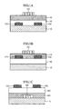
- FIGS. 1A to 1D are sectional views showing the structures of the metal insulator semiconductor field effect transistors (MISFETs) according to an embodiment of the present invention.
- MISFETs metal insulator semiconductor field effect transistors
- a source electrode 120 and a drain electrode 130 may be formed on a substrate 110.
- An active layer 140 may be formed on the substrate 110, provided thereon with the source electrode 120 and the drain electrode 130.
- the substrate 110 a silicon substrate, a semiconductor substrate, a glass substrate, a plastic substrate, metal foil, fabric, paper, or the like may be used.
- an insulating layer 150 may be formed on the active layer 140, and a gate electrode 160 may be formed on the insulating layer 150.
- the width of the gate electrode 160 may be a little greater than the distance between the source electrode 120 and the drain electrode 130.
- the active layer 140 may be formed from solution by applying a colloidal solution in which titanium oxide particles are dispersed or a sol-gel solution including titanium oxide precursors on the substrate 110 provided thereon with the source electrode 120 and the drain electrode 130 using spin coating, dip coating, nano-imprinting, stamping, printing, transfer printing, self-assembly, and the like.
- the active layer 140 may also be formed by depositing from gaseous or solid-state titanium oxides or titanium oxide precursors on the substrate 110 provided thereon with the source electrode 120 and the drain electrode 130 using chemical vapor deposition, laser deposition, thermal evaporation, electron beam evaporation, sputtering, atomic layer deposition, pulsed laser deposition (PLD), and the like.
- chemical vapor deposition laser deposition, thermal evaporation, electron beam evaporation, sputtering, atomic layer deposition, pulsed laser deposition (PLD), and the like.
- titanium oxides are formed preferably into a polycrystalline or amorphous active layer is that it is difficult to form titanium oxides into a single-crystalline active layer, it is difficult to produce transistors having the single-crystalline active layer in large quantities, and it is difficult to integrate the transistors having the single-crystalline active layer into other electronic devices and to utilize them in flexible electronic apparatuses.
- the titanium oxide active layer 140 which is natively n-type in most cases, may be tuned to be more or less conductive or even turned into p-type by adding or mixing with suitable impurities as in conventional semiconductor doping methods. Furthermore, the titanium oxide active layer 140 may be formed by mixing other oxides or metals, for example, SnO 2 InO, ZnO, Al, and the like, with titanium oxides at a predetermined ratio.
- the reason for that is that the performance of the thin film transistor including the titanium oxide active layer can be improved.
- an active layer 140 may be formed on a substrate 110.
- a source electrode 120 and a drain electrode 130 may be formed on the active layer 140.
- An insulating layer 150 may be formed on the active layer 140 provided thereon with the source electrode 120 and the drain electrode 130. Subsequently, a gate electrode 160 may be formed on the insulating layer 150.
- a gate electrode 160 may be formed on a substrate 110.
- An insulating layer 150 may be formed on the substrate 110 provided thereon with the gate electrode 160.
- An active layer 140 may be formed on the insulating layer 150.
- a source electrode 120 and a drain electrode 130 may be formed on the active layer 140.
- a gate electrode 160 may be formed on a substrate 110.
- An insulating layer 150 may be formed on the substrate 110 provided thereon with the gate electrode 160.
- a source electrode 120 and a drain electrode 130 may be formed on the insulating layer 150.
- an active layer 140 may be formed on the insulating layer 150 provided thereon with the source electrode 120 and the drain electrode 130.
- MOSFETs metal semiconductor field effect transistors
- FIGS. 2A to 2D are sectional views showing the structures of the metal semiconductor field effect transistors (MESFETs) according to an embodiment of the present invention.
- MESFETs metal semiconductor field effect transistors
- a source electrode 220 and a drain electrode 230 may be formed on a substrate 210.
- An active layer 240 may be formed on the substrate 210 provided thereon with the source electrode 220 and the drain electrode 230.
- a gate electrode 260 may be formed on the active layer 240.
- the distance between the source electrode 220 and the drain electrode 230 may be the same as or larger than the width of the gate electrode 260.
- an active layer 240 may be formed on a substrate 210.
- a gate electrode 260 may be formed on the active layer 240.
- a source electrode 220 and a drain electrode 230 may be formed on the active layer 240 such that they are disposed at one side and the other side of the gate electrode 260, respectively, at certain intervals.
- a gate electrode 260 may be formed on a substrate 210.
- An active layer 240 may be formed on the substrate 210 provided thereon with the gate electrode 260.
- a source electrode 220 and a drain electrode 230 may be formed on the active layer 240.
- a gate electrode 260 may be formed on a substrate 210.
- a source electrode 220 and a drain electrode 230 may be formed on the substrate 210 such that they are disposed at one side and the other side of the gate electrode 260 at certain intervals, respectively.
- an active layer 240 may be formed on the substrate 210, provided thereon with the gate electrode 260, source electrode 220 and drain electrode 230.
- the present invention provides a novel and cheap transparent metal-oxide thin film transistor (MOxTFT), manufactured based on a TiO 2 active channel layer formed through a solution process. It was found in a real test that n-type TFTs having a charge mobility of 0.12 cm 2 V -1 sec -1 and a threshold voltage of 11 V can be realized by conducting an additional process of diffusing Ti into a TiO 2 channel layer.
- the present invention can also provide a method of extending the scope of the raw material for MOxTFTs and improving their performance in general.
- Titanium dioxide can be produced at low cost in large quantities, and is used in various fields such as pigments, UV-absorbers in cosmetics, photocatalysts, optical coating agents, gas sensors, and the like. Further, titanium dioxide (TiO 2 ) is also being researched in electronics for use as a high-k insulator for manufacturing TFTs, and as an electron transport layer of dye-sensitized cells or organic solar cells.
- TFTs were actually realized using TiO 2 as a raw material for an active channel.
- the present inventors paid attention to the technical and economical potentials that can be expected when TFTs are realized by applying titanium oxides to an active channel layer thereof, based on the facts that TiO 2 is similar to ZnO in the aspect of electron energy bands, such as energy gap, conduction band and valence band, exhibits high hole mobility, can be produced at low cost in large quantities, and can be used in various application fields, as noted above. As a result, the present invention was completed.
- TiO 2 has high resistivity and high trap density, it is difficult in practice to realize effective transistors using TiO 2 thin films or TiO 2 single crystals.
- the trap density of TiO 2 is high, most of the gate voltage-induced carriers cannot efficiently become free carriers, and thus it is very important to decrease the unfilled trap density in channel layers. Both the resistivity and unfilled trap density of TiO 2 can be decreased by externally doping charge carriers.
- the resistivity of titanium oxides can be widely adjusted from that of insulators (10 12 ⁇ cm) to that of conductors (0.001 ⁇ 1 ⁇ cm) through factors such as oxygen vacancy, Ti-interstitials, dopants, and the like. Since films that are resistive or too conductive are not suitable for TFT active channels, in order to realize actually applicable TFTs, an easy process of controlling the optimal doping level must be established.
- the active layer according to the present invention may be formed using the titanium oxides formed by diffusing Ti atoms into titanium oxides.
- the active layer according to the present invention may also be formed by controlling only the oxygen vacancy of titanium oxides without performing the process of diffusing Ti into titanium oxides.
- the present invention provides a method of obtaining a Ti-doped TiO 2 film, including: applying a TiO 2 nanopartic colloidal solution on a SiO 2 (100nm)/Si substrate or a glass substrate through a spin coating process twice to form a thin TiO 2 layer (20 ⁇ 30 nm) ; forming a very thin Ti layer (1 ⁇ 10 nm) on the TiO 2 layer through a thermal evaporation process; treating the TiO 2 layer and Ti layer at a temperature of 550°C ⁇ 800°C for several minutes through a rapid thermal annealing (RTA) process to diffuse Ti into the TiO 2 layer.
- RTA rapid thermal annealing
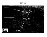
- FIG. 3A and 3B comparing a high resolution transmission electron microscopy (HRTEM) image of a Ti/TiO 2 layer before RTA ( FIG. 3A ) with that of a Ti/TiO 2 layer after RTA ( FIG. 3B ), a Ti layer having a thickness of about 7 nm exists before RTA, but disappears after RTA (550°C, 4 minutes). For this reason, it can be seen that Ti atoms are diffused into the TiO 2 layer after RTA.
- HRTEM transmission electron microscopy
- FIGS. 3A to 3B are views illustrating test results for diffusion procedures according to an embodiment of the present invention.
- a Ti layer is clearly distinguished from a TiO 2 layer before RTA ( FIG. 3A ). That is, the Ti layer shown in the upper portion of FIG. 3A has a selected electron diffraction (SED) pattern typical of amorphous phase. In contrast, the TiO 2 layer, shown in the lower portion of FIG. 3A , has a SED pattern typical of polycrystalline phase.
- SED selected electron diffraction
- the Ti layer is not seen separably from the TiO 2 layer, and the SED pattern of the upper portion of the Ti/TiO 2 layer is not that of an amorphous phase anymore ( FIG. 3B ).
- FIG. 4 is a graph showing test results explaining changes in optical characteristics according to an embodiment of the present invention.
- the transmission of a pure TiO 2 layer is about 98% in the visible light range
- the transmission of a Ti/TiO 2 layer before RTA is decreased from 98% to 94% because a Ti layer placed on the surface of the TiO 2 layer reflects light.
- a TiO 2 layer into which Ti is diffused through RTA exhibits high transmission, the same as that of a pure TiO 2 layer.
- the Ti-diffused TiO 2 layer begins to absorb light at a wavelength corresponding to energy 0.4 eV less than that (3.4 eV) of the pure TiO 2 layer. From the former, it can be seen that Ti is diffused into a TiO 2 layer through RTA without remaining as an additional layer. From the latter, it can be seen that the donor energy level is formed due to the diffusion of Ti.
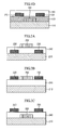
- FIGS. 5A to 5B are views illustrating a TFT having a top-gate structure according to an embodiment of the present invention.
- a TiO 2 channel layer shown in FIGS. 5A to 5B , can be simply formed on a substrate using a serried of process including spin coating, Ti deposition, and RTA.
- the TiO 2 channel layer is formed on a Si wafer including a 100nm-thick thermally grown silicon oxide on its top.
- the thermally grown silicon dioxide layer is only used as a dummy insulating layer.
- substrates such as a glass substrate, etc., may be used as long as they are not damaged at an RTA temperature of 550°C ⁇ 800°C.
- a Ti(5nm)/Au(150nm) layer is formed for the purpose of source/drain contact through thermal evaporation, and the patterning of the formed Ti(5nm)/Au(150nm) layer is conducted through a lift-off process using well-known photolithography.
- source electrode and drain electrode patterns may also be directly formed through printing or shadow masking instead of such a lithographic patterning process.
- a SiO 2 layer having a thickness of 100 nm may be formed as a gate dielectric layer through plasma-enhanced chemical vapor deposition (PECVD).
- PECVD plasma-enhanced chemical vapor deposition
- a Ti(50nm)/Au(150nm) layer may be formed on a gate insulator as a gate metal, and can be patterned using the same method as in the source/drain contact.
- FIG. 6 is a view illustrating a process of manufacturing a TFT according to an embodiment of the present invention.
- a TiO 2 layer may be formed by spin-coating the above mentioned TiO 2 colloidal solution on a SiO 2 /p + -Si substrate or a glass substrate at a rotation speed of 5000 rpm for 30 seconds.
- impurities may be removed from the TiO 2 colloidal solution by filtering the TiO 2 colloidal solution using a PTFE syringe filter having a pore size of 0.2 ⁇ m.
- samples of the formed TiO 2 layer are dried in an oven at 150°C for 1 hour to remove residual water and solvent therefrom.
- Ti titanium
- RTA may be performed at 550°C for 4 minutes, or at 800°C. for 3 minutes.
- Source/drain electrodes may be formed using a photolithographic lift-off treatment.
- the TiO 2 layer/substrate may be spin-coated with a photoresist at a rotation speed of 5000 rpm for 30 seconds, and then the photoresist may be dried on a hot plate at 90°C for 1 minute.
- the samples coated with the photoresist may be dipped in chlorobenzene for 5 minutes in order to realize an overhanging structure on the surface region of a photoresist film.
- the lift-off process can be easily conducted thanks to the overhanging structure.
- these samples may be aligned with a photomask using a contact mask aligner (for example, UV-exposure for 9 seconds).
- a Ti(5nm)/Au(150nm) layer may be deposited thereto through thermal evaporation, and then patterned through a lift-off process using acetone.
- a SiO 2 layer having a thickness of 100 nm may be deposited at a deposition rate of 5 nm/sec through plasma-enhanced chemical vapor deposition (PECVD). Since a Ti(50nm)/Au(150nm) layer may be formed such that Ti is adjacent to the SiO 2 layer, it may be used as a gate metal, and be used to pattern the gate metal through a photolithography process, as in the case of the source/drain electrodes.
- the electrical characteristics of the TFT manufactured through the above processes can be measured using a parametric analyzer. The electrical characteristics thereof will be described with reference to FIGS. 7A to 7D .
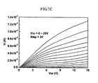
- FIGS. 7A to 7D are graphs illustrating the electrical characteristics of a TFT according to an embodiment of the present invention.
- FIGS. 7A to 7D show the electrical characteristics of the Ti layer having a thickness of 1 nm, which is used for the diffusion of Ti, and the TFT (device A) obtained through RTA at 550°C for 4 minutes.
- This TFT has n-channel enhancement-mode characteristics, particularly pinch-off and saturation characteristics. In particular, current saturation characteristics are very important when the TFT is used as a current source, as in an active-matrix organic display (AMOLED). It again needs to be emphasized that the above mentioned diffusion of Ti is essential in realizing the transistor characteristics. TFTs having an active channel layer made only of pure TiO 2 without performing the Ti diffusion process do not exhibit any appreciable gate-induced modulation characteristics.
- a TFT including a Ti layer having a thickness of 7 nm and having the same process parameters as the device A exhibits gate modulation characteristics, but does not exhibit pinch-off or saturation characteristics. It is presumed that this fact is based on the bulk conductance effect caused by mobile charges of a TiO 2 layer having excessive concentration of Ti atoms.
- FIG. 7B is a graph showing transistor transfer characteristic curves, that is, the characteristics of the current between the source and drain electrodes in relation to the gate voltage. From the transistor transfer characteristic curves, it is estimated that saturation mobility is 0.12 cm 2 V -1 sec -1 and threshold voltage is 17.5 V. Further, it is estimated that the ratio of on/off current is 5 ⁇ 10 3 .
- FIGS. 7C to 7D show the electrical characteristics of the TFT (device B), obtained through RTA at 800°C for 3 minutes instead of at 550°C for 4 minutes, in which the device B is manufactured using the same process as in the device A, except for the RTA. From the data shown in FIGS. 7C to 7D , it is estimated that saturation mobility ( ⁇ e ) is 0.12 cm 2 V -1 sec -1 , threshold voltage (V th ) is 11 V, and that the ratio of on/off current is 4 ⁇ 10 3 .
- other parameters of device B are nearly the same as those of device A, but the threshold voltage (V th ) of device B is clearly different from that of device A. Therefore, it can be presumed that trap density is decreased due to the high-temperature RTA process.
- the thin film transistor (TFT) according to an embodiment of the present invention includes an active channel layer having a thin TiO 2 layer, and was successfully realized.
- the thin film transistor (TFT) according to an embodiment of the present invention is realized by annealing a very thin Ti layer, located on the TiO 2 layer, thus diffusing Ti atoms into the TiO 2 layer. Once traps are filled with the carriers supplied by these Ti atoms, most gate-induced carriers can contribute to the conduction of channels. Meanwhile, it was observed that the threshold voltage was decreased in the high-temperature RTA process. The decrease in threshold voltage can also be influenced by the decrease in initial trap density.
- the results described in this embodiment provide a general approach to improve the performance of MOxTFTs as well as to extend the kinds of raw materials that can be used as active layers in MOxTFTs.
- TiO 2 a cheap and environment-friendly material that can be produced in large quantities and that TiO 2 nanoparticles colloidal solution is easily processed from solution
- the thin film transistor (TFT) according to an embodiment of the present invention can be applied in various fields, as well as in new fields such as transparent electronic devices.
- the performance of the titanium oxide-based TFT can be further improved by optimizing a manufacturing process and utilizing many growth technologies for forming a thin TiO 2 layer. For example, when TiO 2 nanowires are arranged in parallel between a source channel and a drain channel, charges may be transported with less scattering, thus greatly increasing the charge mobility.
- the present invention is advantageous in that a thin film transistor can be manufactured at low cost by forming polycrystalline or amorphous titanium oxides, which are abundant on the Earth and are extremely easy to form into a thin film as an active layer of TFTs.
- the present invention is advantageous in that the harmful environmental problems of conventional thin film transistors can be solved by forming titanium oxides, which are environment-friendly materials, into an active layer of a thin film transistor.
- the present invention is advantageous in that the performance of a thin film transistor, including high charge mobility and resistance to air or moisture, can be improved by forming titanium oxides into an active layer of a thin film transistor.
- the present invention is advantageous in that it can be widely applied to specific electronic apparatuses in which electronic elements and circuits are made invisible by forming transparent titanium oxides into an active layer of a thin film transistor.
Landscapes
- Thin Film Transistor (AREA)
- Liquid Deposition Of Substances Of Which Semiconductor Devices Are Composed (AREA)
- Junction Field-Effect Transistors (AREA)
Abstract
Description
- The present invention relates to a thin film transistor including titanium oxides as an active layer, and especially to its structure and a method of manufacturing the same, which can be used for low-cost production of a thin film transistor, have a potential to solve harmful environmental problems, ' improve the performance of a thin film transistor, and can be widely applied to specific electronic apparatuses.
- Recently, multipurpose displays, which are lightweight, can be increased in size on demand, and can be reduced for easier storage when they are not in use, have attracted a considerable attention in consideration of the benefits such as portability and bidirectional communication. In particular, flexible displays based on organic electroluminescence displays (OLEDs), liquid crystal displays (LCDs), electrophoretic displays, and the like are being developed.
- Organic thin film transistors are particularly attracting attention as driving circuitries in such flexible displays. Organic semiconductors used for organic thin film transistors are mechanically flexible compared to silicon semiconductors. Organic semiconductors have a charge mobility of about 0.001~ several ones cm2/Vsec, and thus are limitedly used only in displays that do not require much current.
- Organic thin film transistors have limited current driving capability due to their limited charge mobility. The current driving capability of organic thin film transistors can be increased to some degree by increasing the ratio of width to length in a channel, but, in this case, there is a problem in that the aperture ratio, which is the ratio of light-emitting area to the total area of a pixel, decreases.
- Furthermore, since organic semiconductors are weakly resistant to oxygen or moisture in the air, it is difficult to realize perfect packaging. Since a flexible substrate has much higher transmissivity of oxygen and moisture than a glass substrate, etc., it is even more challenging to realize a perfect packaging for flexible displays using organic thin film transistors.
- Meanwhile, important transistor technologies include amorphous silicon transistors and low-temperature polysilicon transistors. The amorphous silicon transistors are problematic in that they have low charge mobility and their threshold voltages drift over time. Low-temperature polysilicon transistors are also problematic in that they cannot be used together with plastic substrates that must be handled at temperatures much lower than the processing temperature of low-temperature polysilicon.
- In order to overcome the above problems, transistors based on metal-oxide semiconductors, particularly those based on zinc oxide (ZnO) or its compounds, have been proposed. However, in order to realize a high charge mobility in such metal-oxide transistors, expensive metals, such as indium (In), tin (Sn), gallium (Ga), and the like, are added thereto.
- Such metal-oxide thin film transistors (MOxTFT) have lately attracted considerable attention as alternatives to silicon semiconductor-based TFTs and organic semiconductor-based transistors because they can realize an ideal balance between cost, performance and processibilityin the application fields like active matrix displays, radio frequency identification (RFID) tags, and the like. Further, these MOxTFTs are expected to be applied to new applications in which transparency is required or desired.
- However, as described above, almost all MOxTFTs have been fabricated based on ZnO or mixtures thereof to date. Moreover, since most successful MOxTFTs are mixed with indium, there is a problem in that the material costs and processing costs are high. This presents a great impediment to use in the fields of extremely low-priced goods, such as RFID tags and the like.
- Therefore, efforts have to be made to find novel base materials for realizing thin film transistors with excellent performance and suitable prices and to develop the structures of thin film transistors using the found base materials and methods of manufacturing the same.
- Accordingly, the present invention has been made in an effort to solve the above problems occurring in the prior art, and an object of the present invention is (i) to provide a method of manufacturing a thin film transistor including titanium oxides as an active layer, which can be manufactured at very low cost by using polycrystalline or amorphous titanium oxides, which are abundant on the earth, very easy to form into a thin film, and thus into an active layer of a thin film transistor, and (ii) to provide the structure of the titanium-oxide based thin film transistors manufactured using the method.
- Another object of the present invention is to provide a method of manufacturing a thin film transistor including titanium oxides as an active layer, which can solve the harmful environmental problems of conventional thin film transistors by forming titanium oxides, which are environment-friendly materials, into an active layer of a thin film transistor, and the structure of the thin film transistor manufactured using the method.
- A further object of the present invention is to provide a method of manufacturing a thin film transistor including titanium oxides as an active layer, which can improve the performance of a thin film transistor, including high charge mobility and stability to air or moisture, by forming titanium oxides into an active layer of a thin film transistor, and the structure of the thin film transistor manufactured using the method.
- A still further object of the present invention is to provide a method of manufacturing a thin film transistor including titanium oxides as an active layer, which can be widely applied to specific electronic apparatuses in which electronic should be invisible, by forming transparent titanium oxides into an active layer of a thin film transistor, and the structure of the thin film transistor manufactured using the method.
- In order to accomplish the above objects, a thin film transistor according to an aspect of the present invention provides a thin film transistor, including a substrate, an active layer formed on the substrate using polycrystalline or amorphous titanium oxides, and an insulating layer formed on the active layer.
- In order to accomplish the above objects, a thin film transistor according to another aspect of the present invention provides a thin film transistor, including a substrate, an insulating layer formed on the substrate, and an active layer formed on the insulating layer using polycrystalline or amorphous titanium oxides.
- In order to accomplish the above objects, a thin film transistor according to a further aspect of the present invention provides a thin film transistor, including a substrate, and an active layer formed on the substrate using polycrystalline or amorphous titanium oxides.
- In order to accomplish the above objects, a method of manufacturing a thin film transistor according to a still further aspect of the present invention provides a method of manufacturing a thin film transistor, including: forming a substrate, forming an active layer on the substrate using polycrystalline or amorphous titanium oxides, and forming an insulating layer on the active layer.
- In order to accomplish the above objects, a method of manufacturing a thin film transistor according to a still further aspect of the present invention provides a method of manufacturing a thin film transistor, including: forming a substrate, forming an insulating layer on the substrate, and forming an active layer on the insulating layer using polycrystalline or amorphous titanium oxides.
- In order to accomplish the above objects, a method of manufacturing a thin film transistor according to a still further aspect of the present invention provides a method of manufacturing a thin film transistor, including: forming a substrate, and forming an active layer on the substrate using polycrystalline or amorphous titanium oxides.
- The above and other objects, features and advantages of the present invention will be more clearly understood from the following detailed description taken in conjunction with the accompanying drawings, in which:
-
FIGS. 1A to 1D are sectional views showing structures of metal insulator semiconductor field effect transistors (MISFETs) according to an embodiment of the present invention; -
FIGS. 2A to 2D are sectional views showing structures of metal semiconductor field effect transistors (MESFETs) according to an embodiment of the present invention; -
FIGS. 3A to 3B are views illustrating the test results for diffusion procedures according to an embodiment of the present invention; -
FIG. 4 is a graph showing the test results explaining changes in optical characteristics according to an embodiment of the present invention; -
FIGS. 5A to 5B are views illustrating a TFT having a top-gate structure according to an embodiment of the present invention; -
FIG. 6 is a view illustrating a process of manufacturing a TFT according to an embodiment of the present invention; and -
FIGS. 7A to 7D are graphs illustrating the electrical characteristics of a TFT according to an embodiment of the present invention. - Hereinafter, preferred embodiments of the present invention will be described in detail with reference to the attached drawings.
- Reference now should be made to the drawings, in which the same reference numerals are used throughout the different drawings to designate the same or similar components.
- The present invention provides a method of forming titanium oxides into an amorphous active layer of a thin film transistor. Titanium oxides, which are all kinds of oxides formed by oxidizing titanium, are represented by TiOx (0 < x ≤ 2), for example, TiO2 TiO, etc.
- The thin film transistors according to an embodiment of the present invention may be classified into metal insulator semiconductor field effect transistors (MISFETs) having an insulating layer and metal semiconductor field effect transistors (MESFETs) having no insulating layer.
- The thin film transistor according to an embodiment of the present invention may include all or some of a substrate, an active layer, an insulating layer, a gate electrode, a source electrode, and a drain electrode. Therefore, in the present invention, various types of thin film transistors may be formed depending on the combination of the constituents.
- First, the structures of metal insulator semiconductor field effect transistors (MISFETs) having insulating layers will be described in detail with reference to
FIGS. 1A to 1D . -
FIGS. 1A to 1D are sectional views showing the structures of the metal insulator semiconductor field effect transistors (MISFETs) according to an embodiment of the present invention. - As shown in
FIG. 1A , in a thin film transistor according to an embodiment of the present invention, asource electrode 120 and adrain electrode 130 may be formed on asubstrate 110. Anactive layer 140 may be formed on thesubstrate 110, provided thereon with thesource electrode 120 and thedrain electrode 130. - In this case, as the
substrate 110, a silicon substrate, a semiconductor substrate, a glass substrate, a plastic substrate, metal foil, fabric, paper, or the like may be used. - Subsequently, an insulating
layer 150 may be formed on theactive layer 140, and agate electrode 160 may be formed on the insulatinglayer 150. Here, the width of thegate electrode 160 may be a little greater than the distance between thesource electrode 120 and thedrain electrode 130. - The reason for this is that, although it is ideal if the width of the
gate electrode 160 is identical to the distance between thesource electrode 120 and thedrain electrode 130, in reality, a margin must be provided from the point of view of the manufacture thereof. - In this case, it is proposed in the present invention that titanium oxides be formed into a polycrystalline or amorphous active layer using various conventional coating methods. That is, the
active layer 140 may be formed from solution by applying a colloidal solution in which titanium oxide particles are dispersed or a sol-gel solution including titanium oxide precursors on thesubstrate 110 provided thereon with thesource electrode 120 and thedrain electrode 130 using spin coating, dip coating, nano-imprinting, stamping, printing, transfer printing, self-assembly, and the like. Further, theactive layer 140 may also be formed by depositing from gaseous or solid-state titanium oxides or titanium oxide precursors on thesubstrate 110 provided thereon with thesource electrode 120 and thedrain electrode 130 using chemical vapor deposition, laser deposition, thermal evaporation, electron beam evaporation, sputtering, atomic layer deposition, pulsed laser deposition (PLD), and the like. - The reason why titanium oxides are formed preferably into a polycrystalline or amorphous active layer is that it is difficult to form titanium oxides into a single-crystalline active layer, it is difficult to produce transistors having the single-crystalline active layer in large quantities, and it is difficult to integrate the transistors having the single-crystalline active layer into other electronic devices and to utilize them in flexible electronic apparatuses.
- Further, the titanium oxide
active layer 140, which is natively n-type in most cases, may be tuned to be more or less conductive or even turned into p-type by adding or mixing with suitable impurities as in conventional semiconductor doping methods. Furthermore, the titanium oxideactive layer 140 may be formed by mixing other oxides or metals, for example, SnO2 InO, ZnO, Al, and the like, with titanium oxides at a predetermined ratio. - The reason for that is that the performance of the thin film transistor including the titanium oxide active layer can be improved.
- As shown in
FIG. 1B , in a thin film transistor according to an embodiment of the present invention, anactive layer 140 may be formed on asubstrate 110. Asource electrode 120 and adrain electrode 130 may be formed on theactive layer 140. An insulatinglayer 150 may be formed on theactive layer 140 provided thereon with thesource electrode 120 and thedrain electrode 130. Subsequently, agate electrode 160 may be formed on the insulatinglayer 150. - As shown in
FIG. 1C , in a thin film transistor according to an embodiment of the present invention, agate electrode 160 may be formed on asubstrate 110. An insulatinglayer 150 may be formed on thesubstrate 110 provided thereon with thegate electrode 160. Anactive layer 140 may be formed on the insulatinglayer 150. Subsequently, asource electrode 120 and adrain electrode 130 may be formed on theactive layer 140. - As shown in
FIG. 1D , in a thin film transistor according to an embodiment of the present invention, agate electrode 160 may be formed on asubstrate 110. An insulatinglayer 150 may be formed on thesubstrate 110 provided thereon with thegate electrode 160. Asource electrode 120 and adrain electrode 130 may be formed on the insulatinglayer 150. Subsequently, anactive layer 140 may be formed on the insulatinglayer 150 provided thereon with thesource electrode 120 and thedrain electrode 130. - Next, the structures of metal semiconductor field effect transistors (MESFETs) having no insulating layer will be described in detail with reference to
FIGS. 2A to 2D . -
FIGS. 2A to 2D are sectional views showing the structures of the metal semiconductor field effect transistors (MESFETs) according to an embodiment of the present invention. - As shown in
FIG. 2A , in a thin film transistor according to an embodiment of the present invention, asource electrode 220 and adrain electrode 230 may be formed on asubstrate 210. Anactive layer 240 may be formed on thesubstrate 210 provided thereon with thesource electrode 220 and thedrain electrode 230. - Subsequently, a
gate electrode 260 may be formed on theactive layer 240. Here, the distance between thesource electrode 220 and thedrain electrode 230 may be the same as or larger than the width of thegate electrode 260. - As shown in
FIG. 2B , in a thin film transistor according to an embodiment of the present invention, anactive layer 240 may be formed on asubstrate 210. Agate electrode 260 may be formed on theactive layer 240. Subsequently, asource electrode 220 and adrain electrode 230 may be formed on theactive layer 240 such that they are disposed at one side and the other side of thegate electrode 260, respectively, at certain intervals. - As shown in
FIG. 2C , in a thin film transistor according to an embodiment of the present invention, agate electrode 260 may be formed on asubstrate 210. Anactive layer 240 may be formed on thesubstrate 210 provided thereon with thegate electrode 260. Subsequently, asource electrode 220 and adrain electrode 230 may be formed on theactive layer 240. - As shown in
FIG. 2D , in a thin film transistor according to an embodiment of the present invention, agate electrode 260 may be formed on asubstrate 210. Asource electrode 220 and adrain electrode 230 may be formed on thesubstrate 210 such that they are disposed at one side and the other side of thegate electrode 260 at certain intervals, respectively. Subsequently, anactive layer 240 may be formed on thesubstrate 210, provided thereon with thegate electrode 260,source electrode 220 anddrain electrode 230. - The principle for manufacturing a thin film transistor having an active layer, particularly a TiO2 active layer, a TiO2 active channel or a TiO2 active channel layer, and the test results thereof will be described with reference to
FIGS. 3A to 7D . - The present invention provides a novel and cheap transparent metal-oxide thin film transistor (MOxTFT), manufactured based on a TiO2 active channel layer formed through a solution process. It was found in a real test that n-type TFTs having a charge mobility of 0.12 cm2V-1sec-1 and a threshold voltage of 11 V can be realized by conducting an additional process of diffusing Ti into a TiO2 channel layer. The present invention can also provide a method of extending the scope of the raw material for MOxTFTs and improving their performance in general.
- Titanium dioxide (TiO2) can be produced at low cost in large quantities, and is used in various fields such as pigments, UV-absorbers in cosmetics, photocatalysts, optical coating agents, gas sensors, and the like. Further, titanium dioxide (TiO2) is also being researched in electronics for use as a high-k insulator for manufacturing TFTs, and as an electron transport layer of dye-sensitized cells or organic solar cells.
- However, it has never been reported that TFTs were actually realized using TiO2 as a raw material for an active channel. The present inventors paid attention to the technical and economical potentials that can be expected when TFTs are realized by applying titanium oxides to an active channel layer thereof, based on the facts that TiO2 is similar to ZnO in the aspect of electron energy bands, such as energy gap, conduction band and valence band, exhibits high hole mobility, can be produced at low cost in large quantities, and can be used in various application fields, as noted above. As a result, the present invention was completed.
- It can be seen that, since TiO2 has high resistivity and high trap density, it is difficult in practice to realize effective transistors using TiO2 thin films or TiO2 single crystals. In particular, when the trap density of TiO2 is high, most of the gate voltage-induced carriers cannot efficiently become free carriers, and thus it is very important to decrease the unfilled trap density in channel layers. Both the resistivity and unfilled trap density of TiO2 can be decreased by externally doping charge carriers.
- The resistivity of titanium oxides can be widely adjusted from that of insulators (1012 Ω cm) to that of conductors (0.001 ~ 1 Ω cm) through factors such as oxygen vacancy, Ti-interstitials, dopants, and the like. Since films that are resistive or too conductive are not suitable for TFT active channels, in order to realize actually applicable TFTs, an easy process of controlling the optimal doping level must be established.
- As such, the active layer according to the present invention may be formed using the titanium oxides formed by diffusing Ti atoms into titanium oxides. In addition, the active layer according to the present invention may also be formed by controlling only the oxygen vacancy of titanium oxides without performing the process of diffusing Ti into titanium oxides.
- Therefore, as shown in
FIG. 6 , the present invention provides a method of obtaining a Ti-doped TiO2 film, including: applying a TiO2 nanopartic colloidal solution on a SiO2 (100nm)/Si substrate or a glass substrate through a spin coating process twice to form a thin TiO2 layer (20 ~ 30 nm) ; forming a very thin Ti layer (1 ~ 10 nm) on the TiO2 layer through a thermal evaporation process; treating the TiO2 layer and Ti layer at a temperature of 550°C ~ 800°C for several minutes through a rapid thermal annealing (RTA) process to diffuse Ti into the TiO2 layer. As shown inFIGS. 3A and3B , comparing a high resolution transmission electron microscopy (HRTEM) image of a Ti/TiO2 layer before RTA (FIG. 3A ) with that of a Ti/TiO2 layer after RTA (FIG. 3B ), a Ti layer having a thickness of about 7 nm exists before RTA, but disappears after RTA (550°C, 4 minutes). For this reason, it can be seen that Ti atoms are diffused into the TiO2 layer after RTA. -
FIGS. 3A to 3B are views illustrating test results for diffusion procedures according to an embodiment of the present invention. - As shown in
FIGS. 3A to 3B , a Ti layer is clearly distinguished from a TiO2 layer before RTA (FIG. 3A ). That is, the Ti layer shown in the upper portion ofFIG. 3A has a selected electron diffraction (SED) pattern typical of amorphous phase. In contrast, the TiO2 layer, shown in the lower portion ofFIG. 3A , has a SED pattern typical of polycrystalline phase. - After the RTA, the Ti layer is not seen separably from the TiO2 layer, and the SED pattern of the upper portion of the Ti/TiO2 layer is not that of an amorphous phase anymore (
FIG. 3B ). - Comparing the UV/VIS optical transmission data of Ti(1 nm)/TiO2(25 nm) formed on a glass substrate before RTA with those of Ti(1nm)/TiO2(25nm) formed on a glass substrate after RTA, one can find a clear difference therebetween, and it is described with reference to
FIG. 4 . -
FIG. 4 is a graph showing test results explaining changes in optical characteristics according to an embodiment of the present invention. - As shown in
FIG. 4 , although the transmission of a pure TiO2 layer is about 98% in the visible light range, the transmission of a Ti/TiO2 layer before RTA is decreased from 98% to 94% because a Ti layer placed on the surface of the TiO2 layer reflects light. However, a TiO2 layer into which Ti is diffused through RTA exhibits high transmission, the same as that of a pure TiO2 layer. Further, the Ti-diffused TiO2 layer begins to absorb light at a wavelength corresponding to energy 0.4 eV less than that (3.4 eV) of the pure TiO2 layer. From the former, it can be seen that Ti is diffused into a TiO2 layer through RTA without remaining as an additional layer. From the latter, it can be seen that the donor energy level is formed due to the diffusion of Ti. - The structure of a TFT realized using the above Ti-diffusion phenomenon and the manufacturing principle thereof will be described in detail with reference to
FIGS. 5A to 6 . -
FIGS. 5A to 5B are views illustrating a TFT having a top-gate structure according to an embodiment of the present invention. - As described above, a TiO2 channel layer, shown in
FIGS. 5A to 5B , can be simply formed on a substrate using a serried of process including spin coating, Ti deposition, and RTA. InFIGS. 5A to 5B , the TiO2 channel layer is formed on a Si wafer including a 100nm-thick thermally grown silicon oxide on its top. In this case, the thermally grown silicon dioxide layer is only used as a dummy insulating layer. Various kinds of substrates, such as a glass substrate, etc., may be used as long as they are not damaged at an RTA temperature of 550°C ~ 800°C. - Subsequently, a Ti(5nm)/Au(150nm) layer is formed for the purpose of source/drain contact through thermal evaporation, and the patterning of the formed Ti(5nm)/Au(150nm) layer is conducted through a lift-off process using well-known photolithography. In addition, source electrode and drain electrode patterns may also be directly formed through printing or shadow masking instead of such a lithographic patterning process. After the formation of the source/drain contact, a SiO2 layer having a thickness of 100 nm may be formed as a gate dielectric layer through plasma-enhanced chemical vapor deposition (PECVD). Furthermore, a Ti(50nm)/Au(150nm) layer may be formed on a gate insulator as a gate metal, and can be patterned using the same method as in the source/drain contact.
-
FIG. 6 is a view illustrating a process of manufacturing a TFT according to an embodiment of the present invention. - As shown in
FIG. 6 , first, a TiO2 layer may be formed by spin-coating the above mentioned TiO2 colloidal solution on a SiO2/p+-Si substrate or a glass substrate at a rotation speed of 5000 rpm for 30 seconds. Prior to the spin-coating of the TiO2 colloidal solution, impurities may be removed from the TiO2 colloidal solution by filtering the TiO2 colloidal solution using a PTFE syringe filter having a pore size of 0.2 µm. Subsequently, samples of the formed TiO2 layer are dried in an oven at 150°C for 1 hour to remove residual water and solvent therefrom. Thereafter, a very thin titanium (Ti) layer may be thermally deposited on the TiO2 layer at a deposition rate of 0.2 Å/sec under a pressure of 8×10⁻⁷ torr. Then, RTA may be performed at 550°C for 4 minutes, or at 800°C. for 3 minutes. - Source/drain electrodes may be formed using a photolithographic lift-off treatment. The TiO2 layer/substrate may be spin-coated with a photoresist at a rotation speed of 5000 rpm for 30 seconds, and then the photoresist may be dried on a hot plate at 90°C for 1 minute. Prior to patterning, the samples coated with the photoresist may be dipped in chlorobenzene for 5 minutes in order to realize an overhanging structure on the surface region of a photoresist film. The lift-off process can be easily conducted thanks to the overhanging structure. Further, these samples may be aligned with a photomask using a contact mask aligner (for example, UV-exposure for 9 seconds).
- After the source/drain patterns of the photoresist are formed using a developer, a Ti(5nm)/Au(150nm) layer may be deposited thereto through thermal evaporation, and then patterned through a lift-off process using acetone. A SiO2 layer having a thickness of 100 nm may be deposited at a deposition rate of 5 nm/sec through plasma-enhanced chemical vapor deposition (PECVD). Since a Ti(50nm)/Au(150nm) layer may be formed such that Ti is adjacent to the SiO2 layer, it may be used as a gate metal, and be used to pattern the gate metal through a photolithography process, as in the case of the source/drain electrodes.
- The electrical characteristics of the TFT manufactured through the above processes can be measured using a parametric analyzer. The electrical characteristics thereof will be described with reference to
FIGS. 7A to 7D . -
FIGS. 7A to 7D are graphs illustrating the electrical characteristics of a TFT according to an embodiment of the present invention. -
FIGS. 7A to 7D show the electrical characteristics of the Ti layer having a thickness of 1 nm, which is used for the diffusion of Ti, and the TFT (device A) obtained through RTA at 550°C for 4 minutes. This TFT has n-channel enhancement-mode characteristics, particularly pinch-off and saturation characteristics. In particular, current saturation characteristics are very important when the TFT is used as a current source, as in an active-matrix organic display (AMOLED). It again needs to be emphasized that the above mentioned diffusion of Ti is essential in realizing the transistor characteristics. TFTs having an active channel layer made only of pure TiO2 without performing the Ti diffusion process do not exhibit any appreciable gate-induced modulation characteristics. - Further, it was observed that the optimal thickness of the initial Ti layer in the Ti diffusion process is important to realize a desired TFT characteristic. For example, a TFT including a Ti layer having a thickness of 7 nm and having the same process parameters as the device A exhibits gate modulation characteristics, but does not exhibit pinch-off or saturation characteristics. It is presumed that this fact is based on the bulk conductance effect caused by mobile charges of a TiO2 layer having excessive concentration of Ti atoms.
-
FIG. 7B is a graph showing transistor transfer characteristic curves, that is, the characteristics of the current between the source and drain electrodes in relation to the gate voltage. From the transistor transfer characteristic curves, it is estimated that saturation mobility is 0.12 cm2V-1 sec-1 and threshold voltage is 17.5 V. Further, it is estimated that the ratio of on/off current is 5×10³. -
FIGS. 7C to 7D show the electrical characteristics of the TFT (device B), obtained through RTA at 800°C for 3 minutes instead of at 550°C for 4 minutes, in which the device B is manufactured using the same process as in the device A, except for the RTA. From the data shown inFIGS. 7C to 7D , it is estimated that saturation mobility (µe) is 0.12 cm2V-1sec-1, threshold voltage (Vth) is 11 V, and that the ratio of on/off current is 4×10³. Here, other parameters of device B are nearly the same as those of device A, but the threshold voltage (Vth) of device B is clearly different from that of device A. Therefore, it can be presumed that trap density is decreased due to the high-temperature RTA process. - The thin film transistor (TFT) according to an embodiment of the present invention includes an active channel layer having a thin TiO2 layer, and was successfully realized. The thin film transistor (TFT) according to an embodiment of the present invention is realized by annealing a very thin Ti layer, located on the TiO2 layer, thus diffusing Ti atoms into the TiO2 layer. Once traps are filled with the carriers supplied by these Ti atoms, most gate-induced carriers can contribute to the conduction of channels. Meanwhile, it was observed that the threshold voltage was decreased in the high-temperature RTA process. The decrease in threshold voltage can also be influenced by the decrease in initial trap density.
- The results described in this embodiment provide a general approach to improve the performance of MOxTFTs as well as to extend the kinds of raw materials that can be used as active layers in MOxTFTs. Considering that TiO2 a cheap and environment-friendly material that can be produced in large quantities and that TiO2 nanoparticles colloidal solution is easily processed from solution, it is expected that the thin film transistor (TFT) according to an embodiment of the present invention can be applied in various fields, as well as in new fields such as transparent electronic devices. The performance of the titanium oxide-based TFT can be further improved by optimizing a manufacturing process and utilizing many growth technologies for forming a thin TiO2 layer. For example, when TiO2 nanowires are arranged in parallel between a source channel and a drain channel, charges may be transported with less scattering, thus greatly increasing the charge mobility.
- As described above, the present invention is advantageous in that a thin film transistor can be manufactured at low cost by forming polycrystalline or amorphous titanium oxides, which are abundant on the Earth and are extremely easy to form into a thin film as an active layer of TFTs.
- Further, the present invention is advantageous in that the harmful environmental problems of conventional thin film transistors can be solved by forming titanium oxides, which are environment-friendly materials, into an active layer of a thin film transistor.
- Further, the present invention is advantageous in that the performance of a thin film transistor, including high charge mobility and resistance to air or moisture, can be improved by forming titanium oxides into an active layer of a thin film transistor.
- Furthermore, the present invention is advantageous in that it can be widely applied to specific electronic apparatuses in which electronic elements and circuits are made invisible by forming transparent titanium oxides into an active layer of a thin film transistor.
- Although the preferred embodiments of the present invention have been disclosed for illustrative purposes, those skilled in the art will appreciate that various modifications, additions and substitutions are possible, without departing from the scope and spirit of the invention as disclosed in the accompanying claims.
Claims (38)
- A thin film transistor, comprising:a substrate;an active layer formed on the substrate using polycrystalline or amorphous titanium oxides; andan insulating layer formed on the active layer.
- The thin film transistor according to claim 1, further comprising:a gate electrode formed on the insulating layer; anda source electrode and a drain electrode formed on the substrate and covered with the active layer.
- The thin film transistor according to claim 1, further comprising:a gate electrode formed on the insulating layer; anda source electrode and a drain electrode formed on the active layer and covered with the insulating layer.
- The thin film transistor according to claim 1, wherein the active layer is formed using Ti-doped TiOx obtained by diffusing titanium (Ti) atoms into polycrystalline or amorphous titanium oxides (TiOx, 0<x≤2).
- The thin film transistor according to claim 4, wherein the active layer is formed using Ti-doped TiOx obtained by forming a titanium (Ti) layer on a titanium oxide layer through a thermal evaporation process and then performing treatment through a thermal annealing process.
- The thin film transistor according to claim 5, wherein the titanium (Ti) layer is formed between the titanium oxide layers, or thereon or therebeneath through the thermal evaporation process.
- The thin film transistor according to claim 1, wherein the titanium oxides are all kinds of oxides formed by oxidizing titanium, and are represented by TiOx (0 < x ≤ 2).
- The thin film transistor according to claim 7, wherein the active layer is formed using N-type titanium oxides or P-type titanium oxides, obtained through an impurity doping process of mixing oxides or metals with the titanium oxides.
- The thin film transistor according to claim 7, wherein the active layer is formed by controlling the oxygen vacancy of the titanium oxides.
- The thin film transistor according to claim 1, wherein the active layer is formed using any one selected from among spin coating, dip coating, imprinting, stamping, printing, transfer printing, self-assembly, chemical vapor deposition, room-temperature or high-temperature deposition, thermal evaporation, electron beam evaporation, sputtering, atomic layer deposition, and pulsed laser deposition (PLD).
- The thin film transistor according to claim 1, wherein the substrate is formed using any one selected from among a silicon substrate, a semiconductor substrate, a glass substrate, a plastic substrate, metal foil, fabric, and paper.
- A thin film transistor, comprising:a substrate;an insulating layer formed on the substrate; andan active layer formed on the insulating layer using polycrystalline or amorphous titanium oxides.
- The thin film transistor according to claim 12, further comprising:a gate electrode formed on the substrate and covered with the insulating layer; anda source electrode and a drain electrode formed on the active layer.
- The thin film transistor according to claim 12, further comprising:a gate electrode formed on the substrate and covered with the insulating layer; anda source electrode and a drain electrode formed on the insulating layer.
- A thin film transistor, comprising:a substrate; andan active layer formed on the substrate using polycrystalline or amorphous titanium oxides.
- The thin film transistor according to claim 15, further comprising:a gate electrode formed on the active layer; anda source electrode and a drain electrode formed on the substrate and covered with the active layer.
- The thin film transistor according to claim 15, further comprising:a gate electrode formed on the active layer; anda source electrode and a drain electrode formed on the active layer such that they are disposed at one side and another side of the gate electrode, respectively, at a certain interval.
- The thin film transistor according to claim 15, further comprising:a gate electrode formed on the substrate and covered with the active layer; anda source electrode and a drain electrode formed on the active layer.
- The thin film transistor according to claim 15, further comprising:a gate electrode formed on the substrate and covered with the active layer; anda source electrode and a drain electrode formed on the substrate and covered with the active layer such that they are disposed at one side and other side of the gate electrode at a certain interval, respectively.
- A method of manufacturing a thin film transistor, comprising:forming a substrate;forming an active layer on the substrate using polycrystalline or amorphous titanium oxides; andforming an insulating layer on the active layer.
- The method of manufacturing a thin film transistor according to claim 20, further comprising:forming a source electrode and a drain electrode on the substrate; andforming a gate electrode on the insulating layer,wherein the source electrode and the drain electrode are covered with the active layer.
- The method of manufacturing a thin film transistor according to claim 20, further comprising:forming a source electrode and a drain electrode on the active layer; andforming a gate electrode on the insulating layer,wherein the source electrode and the drain electrode are covered with the insulating layer.
- The method of manufacturing a thin film transistor according to claim 20, wherein the active layer is formed using Ti-doped TiOx obtained by diffusing titanium (Ti) atoms into polycrystalline or amorphous titanium oxides (TiOx, 0<x≤2).
- The method of manufacturing a thin film transistor according to claim 23, wherein the active layer is formed using Ti-doped TiOx obtained by forming a titanium (Ti) layer on a titanium oxide layer through a thermal evaporation process and then performing treatment through a thermal annealing process.
- The method of manufacturing a thin film transistor according to claim 24, wherein the titanium (Ti) layer is formed between the titanium oxide layers, or thereon or therebeneath through the thermal evaporation process.
- The method of manufacturing a thin film transistor according to claim 20, wherein the titanium oxides are all kinds of oxides formed by oxidizing titanium, and are represented by TiOx (0 < x ≤ 2).
- The method of manufacturing a thin film transistor according to claim 26, wherein the active layer is formed using n-type titanium oxides or p-type titanium oxides obtained through an impurity doping process of mixing oxides or metals with the titanium oxides.
- The method of manufacturing a thin film transistor according to claim 26, wherein the active layer is formed by controlling the oxygen vacancy of the titanium oxides.
- The method of manufacturing a thin film transistor according to claim 20, wherein the active layer is formed using any one selected from among spin coating, dip coating, imprinting, stamping, printing, transfer printing, self-assembly, chemical vapor deposition, room-temperature or high-temperature deposition, thermal evaporation, electron beam evaporation, sputtering, atomic layer deposition, and pulsed laser deposition (PLD).
- The method of manufacturing a thin film transistor according to claim 20, wherein the substrate is formed using any one selected from among a silicon substrate, a semiconductor substrate, a glass substrate, a plastic substrate, metal foil, fabric, and paper.
- A method of manufacturing a thin film transistor, comprising:forming a substrate;forming an insulating layer on the substrate; andforming an active layer on the insulating layer using polycrystalline or amorphous titanium oxides.
- The method of manufacturing a thin film transistor according to claim 31, further comprising:forming a gate electrode on the substrate; andforming a source electrode and a drain electrode on the active layer,wherein the gate electrode is covered with the insulating layer.
- The method of manufacturing a thin film transistor according to claim 31, further comprising:forming a gate electrode on the substrate; andforming a source electrode and a drain electrode on the insulating layer,wherein the gate electrode is covered with the insulating layer.
- A method of manufacturing a thin film transistor, comprising:forming a substrate; andforming an active layer on the substrate using polycrystalline or amorphous titanium oxides.
- The method of manufacturing a thin film transistor according to claim 34, further comprising:forming a source electrode and a drain electrode on the substrate; andforming a gate electrode on the active layer,wherein the source electrode and the drain electrode are covered with the active layer.
- The method of manufacturing a thin film transistor according to claim 34, further comprising:forming a gate electrode on the active layer; andforming a source electrode and a drain electrode on the active layer such that they are disposed at one side and other side of the gate electrode at a certain interval, respectively.
- The method of manufacturing a thin film transistor according to claim 34, further comprising:forming a gate electrode on the substrate; andforming a source electrode and a drain electrode on the active layer,wherein the gate electrode is covered with the active layer.
- The method of manufacturing a thin film transistor according to claim 34, further comprising:forming a gate electrode on the substrate; andforming a source electrode and a drain electrode on the substrate such that they are disposed at one side and another side, respectively, of the gate electrode at a certain interval,wherein the gate electrode, source electrode and drain electrode are covered with the active layer.
Applications Claiming Priority (2)
| Application Number | Priority Date | Filing Date | Title |
|---|---|---|---|
| KR20070031144 | 2007-03-29 | ||
| KR1020070101638A KR100930057B1 (en) | 2007-03-29 | 2007-10-09 | Fabrication method and structure thereof of thin film transistor having titanium oxide as active layer |
Publications (2)
| Publication Number | Publication Date |
|---|---|
| EP1976019A1 true EP1976019A1 (en) | 2008-10-01 |
| EP1976019B1 EP1976019B1 (en) | 2011-06-15 |
Family
ID=39590150
Family Applications (1)
| Application Number | Title | Priority Date | Filing Date |
|---|---|---|---|
| EP08005930A Not-in-force EP1976019B1 (en) | 2007-03-29 | 2008-03-28 | Thin film transistor including titanium oxides as active layer and method of manufacturing the same |
Country Status (3)
| Country | Link |
|---|---|
| US (1) | US7768042B2 (en) |
| EP (1) | EP1976019B1 (en) |
| JP (1) | JP2008252097A (en) |
Cited By (2)
| Publication number | Priority date | Publication date | Assignee | Title |
|---|---|---|---|---|
| US8957415B2 (en) | 2012-05-21 | 2015-02-17 | Samsung Display Co., Ltd. | Thin film transistor and thin film transistor array panel including the same |
| CN105658733A (en) * | 2013-06-06 | 2016-06-08 | 霍尼韦尔国际公司 | Liquid titanium oxide compositions, methods for forming the same, and methods for etching material layers of or overlying substrates using the same |
Families Citing this family (13)
| Publication number | Priority date | Publication date | Assignee | Title |
|---|---|---|---|---|
| US6998656B2 (en) * | 2003-02-07 | 2006-02-14 | Hewlett-Packard Development Company, L.P. | Transparent double-injection field-effect transistor |
| US7808387B1 (en) * | 2007-06-07 | 2010-10-05 | Impinj, Inc. | Voltage reference circuit with low-power bandgap |
| KR20110090408A (en) * | 2010-02-03 | 2011-08-10 | 삼성전자주식회사 | Thin film forming method, metal wiring for display panel, thin film transistor array panel comprising same and manufacturing method thereof |
| JP5776192B2 (en) | 2010-02-16 | 2015-09-09 | 株式会社リコー | Field effect transistor, display element, image display apparatus and system |
| KR102090289B1 (en) | 2013-05-30 | 2020-04-16 | 삼성디스플레이 주식회사 | Oxide sputtering target, thin film transistor using the same and method for manufacturing thin film transistor |
| US9754802B2 (en) | 2013-07-11 | 2017-09-05 | Yissum Research Development Company Of The Hebrew University Of Jerusalem Ltd. | Thermal doping by vacancy formation in nanocrystals |
| FR3009652B1 (en) | 2013-08-08 | 2016-10-21 | Commissariat Energie Atomique | METHOD FOR MANUFACTURING ORGANIC CMOS CIRCUIT AND ORGANIC CMOS CIRCUIT PROTECTED AGAINST UV |
| CN105097824B (en) * | 2014-05-22 | 2019-12-10 | 群创光电股份有限公司 | Thin film transistor substrate, manufacturing method thereof and display |
| CN104143575A (en) * | 2014-07-25 | 2014-11-12 | 京东方科技集团股份有限公司 | Thin film transistor, array substrate and display device |
| KR101680433B1 (en) | 2014-11-25 | 2016-11-29 | 순천대학교 산학협력단 | Manufacturing method of roll-to-roll gravure printed thin film transistor, thin film transistor backplane, backplane pressure sensor and smart sheet |
| US10141183B2 (en) * | 2016-01-28 | 2018-11-27 | Tokyo Electron Limited | Methods of spin-on deposition of metal oxides |
| CN105977304B (en) * | 2016-05-31 | 2019-01-11 | 京东方科技集团股份有限公司 | Transistor, its manufacturing method, array substrate, display panel and display device |
| CN112447858B (en) * | 2020-10-29 | 2022-09-20 | 南京理工大学 | Junction field effect transistor and preparation method thereof |
Citations (2)
| Publication number | Priority date | Publication date | Assignee | Title |
|---|---|---|---|---|
| WO2006051993A2 (en) | 2004-11-10 | 2006-05-18 | Canon Kabushiki Kaisha | Amorphous oxide and field effect transistor |
| WO2006103853A1 (en) | 2005-03-25 | 2006-10-05 | Japan Science And Technology Agency | Semiconductor device using titanium dioxide as active layer and method for manufacturing same |
Family Cites Families (13)
| Publication number | Priority date | Publication date | Assignee | Title |
|---|---|---|---|---|
| JP3079535B2 (en) | 1990-02-07 | 2000-08-21 | スズキ株式会社 | Manufacturing method of semiconductor thin film |
| US5625199A (en) * | 1996-01-16 | 1997-04-29 | Lucent Technologies Inc. | Article comprising complementary circuit with inorganic n-channel and organic p-channel thin film transistors |
| JP3830623B2 (en) * | 1997-07-14 | 2006-10-04 | 株式会社半導体エネルギー研究所 | Method for manufacturing crystalline semiconductor film |
| KR100450786B1 (en) | 1998-03-09 | 2004-12-17 | 삼성전자주식회사 | A light enhanced Ti/TiOx/Ti based field effect transistor and a fabricating method thereof |
| JP2003518754A (en) * | 1999-12-21 | 2003-06-10 | プラスティック ロジック リミテッド | Solution-processed device |
| JP4102880B2 (en) * | 2004-02-23 | 2008-06-18 | 国立大学法人東北大学 | Multilayer structure and element structure |
| US7378286B2 (en) * | 2004-08-20 | 2008-05-27 | Sharp Laboratories Of America, Inc. | Semiconductive metal oxide thin film ferroelectric memory transistor |
| JP5138163B2 (en) * | 2004-11-10 | 2013-02-06 | キヤノン株式会社 | Field effect transistor |
| JP2006286681A (en) * | 2005-03-31 | 2006-10-19 | Kyushu Institute Of Technology | Field effect transistor and manufacturing method thereof |
| US20060231829A1 (en) * | 2005-04-13 | 2006-10-19 | Xerox Corporation | TFT gate dielectric with crosslinked polymer |
| US7456104B2 (en) * | 2005-05-31 | 2008-11-25 | Semiconductor Energy Laboratory Co., Ltd. | Semiconductor device and manufacturing method thereof |
| JP5116225B2 (en) * | 2005-09-06 | 2013-01-09 | キヤノン株式会社 | Manufacturing method of oxide semiconductor device |
| JP2009536445A (en) * | 2006-01-04 | 2009-10-08 | ザ リージェンツ オブ ザ ユニバーシティ オブ カリフォルニア | Passive layer for flexible electronic devices |
-
2008
- 2008-03-28 EP EP08005930A patent/EP1976019B1/en not_active Not-in-force
- 2008-03-28 US US12/058,399 patent/US7768042B2/en active Active
- 2008-03-31 JP JP2008091824A patent/JP2008252097A/en active Pending
Patent Citations (2)
| Publication number | Priority date | Publication date | Assignee | Title |
|---|---|---|---|---|
| WO2006051993A2 (en) | 2004-11-10 | 2006-05-18 | Canon Kabushiki Kaisha | Amorphous oxide and field effect transistor |
| WO2006103853A1 (en) | 2005-03-25 | 2006-10-05 | Japan Science And Technology Agency | Semiconductor device using titanium dioxide as active layer and method for manufacturing same |
Cited By (2)
| Publication number | Priority date | Publication date | Assignee | Title |
|---|---|---|---|---|
| US8957415B2 (en) | 2012-05-21 | 2015-02-17 | Samsung Display Co., Ltd. | Thin film transistor and thin film transistor array panel including the same |
| CN105658733A (en) * | 2013-06-06 | 2016-06-08 | 霍尼韦尔国际公司 | Liquid titanium oxide compositions, methods for forming the same, and methods for etching material layers of or overlying substrates using the same |
Also Published As
| Publication number | Publication date |
|---|---|
| US7768042B2 (en) | 2010-08-03 |
| JP2008252097A (en) | 2008-10-16 |
| EP1976019B1 (en) | 2011-06-15 |
| US20080237595A1 (en) | 2008-10-02 |
Similar Documents
| Publication | Publication Date | Title |
|---|---|---|
| US7768042B2 (en) | Thin film transistor including titanium oxides as active layer and method of manufacturing the same | |
| KR101482944B1 (en) | method for manufacturing thin film transistors based on titanium oxides as active layer and thin film transistors thereof | |
| Lee et al. | 15.4: Excellent Performance of Indium‐Oxide‐Based Thin‐Film Transistors by DC Sputtering | |
| US8324628B2 (en) | Channel layer for a thin film transistor, thin film transistor including the same, and methods of manufacturing the same | |
| US20060270197A1 (en) | Compound semiconductor material and method for forming an active layer of a thin film transistor device | |
| US10461100B2 (en) | Display device having a different type of oxide semiconductor transistor | |
| JPWO2014136636A1 (en) | Thin film transistor | |
| US11843057B2 (en) | Oxide semiconductor transistor having dual gate structure and method of fabricating the same | |
| CN101047130B (en) | Top-gate thin-film transistors using nanoparticles and method of manufacturing the same | |
| KR100983544B1 (en) | Method for manufacturing thin film transistor having titanium oxide as active layer and its structure | |
| US9093536B2 (en) | Thin film transistor substrate and method of manufacturing the same | |
| Park et al. | New n-Type $\hbox {TiO} _ {2} $ Transparent Active Channel TFTs Fabricated With a Solution Process | |
| US7972931B2 (en) | Top-gate thin-film transistors using nanoparticles and method of manufacturing the same | |
| KR100930057B1 (en) | Fabrication method and structure thereof of thin film transistor having titanium oxide as active layer | |
| US20080210934A1 (en) | Semiconductor Device Using Titanium Dioxide as Active Layer and Method for Producing Semiconductor Device | |
| US8120029B2 (en) | Thin film transistor and method of manufacturing the same | |
| Ryu et al. | Solution‐processed oxide semiconductors for low‐cost and high‐performance thin‐film transistors and fabrication of organic light‐emitting‐diode displays | |
| KR102036972B1 (en) | Oxide thin film transistor and method of manufacturing the same | |
| CN102194888B (en) | Thin film transistor and its manufacture method | |
| KR102884720B1 (en) | Vertical Thin Film Transistor and method of manufacturing for the same | |
| KR100792407B1 (en) | Front gate thin film transistor using nanoparticles on flexible substrate and its manufacturing method | |
| US20080283874A1 (en) | Field-Effect Transistors | |
| Uprety | Electrical characteristics of thin-film transistors (TFTs) based on the solution-processed Zinc Tin Oxide (ZTO) channel layer | |
| KR20080111736A (en) | Oxide semiconductor and thin film transistor comprising the same | |
| Salas-Villasenor | Chalcogenide based materials and devices for flexible electronics applications |
Legal Events
| Date | Code | Title | Description |
|---|---|---|---|
| PUAI | Public reference made under article 153(3) epc to a published international application that has entered the european phase |
Free format text: ORIGINAL CODE: 0009012 |
|
| AK | Designated contracting states |
Kind code of ref document: A1 Designated state(s): AT BE BG CH CY CZ DE DK EE ES FI FR GB GR HR HU IE IS IT LI LT LU LV MC MT NL NO PL PT RO SE SI SK TR |
|
| AX | Request for extension of the european patent |
Extension state: AL BA MK RS |
|
| 17P | Request for examination filed |
Effective date: 20090401 |
|
| 17Q | First examination report despatched |
Effective date: 20090504 |
|
| AKX | Designation fees paid |
Designated state(s): AT BE BG CH CY CZ DE DK EE ES FI FR GB GR HR HU IE IS IT LI LT LU LV MC MT NL NO PL PT RO SE SI SK TR |
|
| GRAP | Despatch of communication of intention to grant a patent |
Free format text: ORIGINAL CODE: EPIDOSNIGR1 |
|
| GRAS | Grant fee paid |
Free format text: ORIGINAL CODE: EPIDOSNIGR3 |
|
| GRAA | (expected) grant |
Free format text: ORIGINAL CODE: 0009210 |
|
| AK | Designated contracting states |
Kind code of ref document: B1 Designated state(s): AT BE BG CH CY CZ DE DK EE ES FI FR GB GR HR HU IE IS IT LI LT LU LV MC MT NL NO PL PT RO SE SI SK TR |
|
| REG | Reference to a national code |
Ref country code: GB Ref legal event code: FG4D Ref country code: CH Ref legal event code: EP |
|
| REG | Reference to a national code |
Ref country code: IE Ref legal event code: FG4D |
|
| REG | Reference to a national code |
Ref country code: DE Ref legal event code: R096 Ref document number: 602008007527 Country of ref document: DE Effective date: 20110728 |
|
| REG | Reference to a national code |
Ref country code: NL Ref legal event code: VDEP Effective date: 20110615 |
|
| PG25 | Lapsed in a contracting state [announced via postgrant information from national office to epo] |
Ref country code: HR Free format text: LAPSE BECAUSE OF FAILURE TO SUBMIT A TRANSLATION OF THE DESCRIPTION OR TO PAY THE FEE WITHIN THE PRESCRIBED TIME-LIMIT Effective date: 20110615 Ref country code: SE Free format text: LAPSE BECAUSE OF FAILURE TO SUBMIT A TRANSLATION OF THE DESCRIPTION OR TO PAY THE FEE WITHIN THE PRESCRIBED TIME-LIMIT Effective date: 20110615 Ref country code: NO Free format text: LAPSE BECAUSE OF FAILURE TO SUBMIT A TRANSLATION OF THE DESCRIPTION OR TO PAY THE FEE WITHIN THE PRESCRIBED TIME-LIMIT Effective date: 20110915 Ref country code: LT Free format text: LAPSE BECAUSE OF FAILURE TO SUBMIT A TRANSLATION OF THE DESCRIPTION OR TO PAY THE FEE WITHIN THE PRESCRIBED TIME-LIMIT Effective date: 20110615 |
|
| PG25 | Lapsed in a contracting state [announced via postgrant information from national office to epo] |
Ref country code: FI Free format text: LAPSE BECAUSE OF FAILURE TO SUBMIT A TRANSLATION OF THE DESCRIPTION OR TO PAY THE FEE WITHIN THE PRESCRIBED TIME-LIMIT Effective date: 20110615 Ref country code: AT Free format text: LAPSE BECAUSE OF FAILURE TO SUBMIT A TRANSLATION OF THE DESCRIPTION OR TO PAY THE FEE WITHIN THE PRESCRIBED TIME-LIMIT Effective date: 20110615 Ref country code: LV Free format text: LAPSE BECAUSE OF FAILURE TO SUBMIT A TRANSLATION OF THE DESCRIPTION OR TO PAY THE FEE WITHIN THE PRESCRIBED TIME-LIMIT Effective date: 20110615 Ref country code: CY Free format text: LAPSE BECAUSE OF FAILURE TO SUBMIT A TRANSLATION OF THE DESCRIPTION OR TO PAY THE FEE WITHIN THE PRESCRIBED TIME-LIMIT Effective date: 20110615 Ref country code: GR Free format text: LAPSE BECAUSE OF FAILURE TO SUBMIT A TRANSLATION OF THE DESCRIPTION OR TO PAY THE FEE WITHIN THE PRESCRIBED TIME-LIMIT Effective date: 20110916 Ref country code: SI Free format text: LAPSE BECAUSE OF FAILURE TO SUBMIT A TRANSLATION OF THE DESCRIPTION OR TO PAY THE FEE WITHIN THE PRESCRIBED TIME-LIMIT Effective date: 20110615 |
|
| PG25 | Lapsed in a contracting state [announced via postgrant information from national office to epo] |
Ref country code: NL Free format text: LAPSE BECAUSE OF FAILURE TO SUBMIT A TRANSLATION OF THE DESCRIPTION OR TO PAY THE FEE WITHIN THE PRESCRIBED TIME-LIMIT Effective date: 20110615 Ref country code: BE Free format text: LAPSE BECAUSE OF FAILURE TO SUBMIT A TRANSLATION OF THE DESCRIPTION OR TO PAY THE FEE WITHIN THE PRESCRIBED TIME-LIMIT Effective date: 20110615 |
|
| PG25 | Lapsed in a contracting state [announced via postgrant information from national office to epo] |
Ref country code: EE Free format text: LAPSE BECAUSE OF FAILURE TO SUBMIT A TRANSLATION OF THE DESCRIPTION OR TO PAY THE FEE WITHIN THE PRESCRIBED TIME-LIMIT Effective date: 20110615 Ref country code: CZ Free format text: LAPSE BECAUSE OF FAILURE TO SUBMIT A TRANSLATION OF THE DESCRIPTION OR TO PAY THE FEE WITHIN THE PRESCRIBED TIME-LIMIT Effective date: 20110615 Ref country code: PT Free format text: LAPSE BECAUSE OF FAILURE TO SUBMIT A TRANSLATION OF THE DESCRIPTION OR TO PAY THE FEE WITHIN THE PRESCRIBED TIME-LIMIT Effective date: 20111017 Ref country code: IS Free format text: LAPSE BECAUSE OF FAILURE TO SUBMIT A TRANSLATION OF THE DESCRIPTION OR TO PAY THE FEE WITHIN THE PRESCRIBED TIME-LIMIT Effective date: 20111015 |
|
| PG25 | Lapsed in a contracting state [announced via postgrant information from national office to epo] |
Ref country code: RO Free format text: LAPSE BECAUSE OF FAILURE TO SUBMIT A TRANSLATION OF THE DESCRIPTION OR TO PAY THE FEE WITHIN THE PRESCRIBED TIME-LIMIT Effective date: 20110615 Ref country code: PL Free format text: LAPSE BECAUSE OF FAILURE TO SUBMIT A TRANSLATION OF THE DESCRIPTION OR TO PAY THE FEE WITHIN THE PRESCRIBED TIME-LIMIT Effective date: 20110615 Ref country code: SK Free format text: LAPSE BECAUSE OF FAILURE TO SUBMIT A TRANSLATION OF THE DESCRIPTION OR TO PAY THE FEE WITHIN THE PRESCRIBED TIME-LIMIT Effective date: 20110615 |
|
| PLBE | No opposition filed within time limit |
Free format text: ORIGINAL CODE: 0009261 |
|
| STAA | Information on the status of an ep patent application or granted ep patent |
Free format text: STATUS: NO OPPOSITION FILED WITHIN TIME LIMIT |
|
| 26N | No opposition filed |
Effective date: 20120316 |
|
| PG25 | Lapsed in a contracting state [announced via postgrant information from national office to epo] |
Ref country code: IT Free format text: LAPSE BECAUSE OF FAILURE TO SUBMIT A TRANSLATION OF THE DESCRIPTION OR TO PAY THE FEE WITHIN THE PRESCRIBED TIME-LIMIT Effective date: 20110615 |
|
| PG25 | Lapsed in a contracting state [announced via postgrant information from national office to epo] |
Ref country code: DK Free format text: LAPSE BECAUSE OF FAILURE TO SUBMIT A TRANSLATION OF THE DESCRIPTION OR TO PAY THE FEE WITHIN THE PRESCRIBED TIME-LIMIT Effective date: 20110615 |
|
| REG | Reference to a national code |
Ref country code: DE Ref legal event code: R097 Ref document number: 602008007527 Country of ref document: DE Effective date: 20120316 |
|
| PG25 | Lapsed in a contracting state [announced via postgrant information from national office to epo] |
Ref country code: MC Free format text: LAPSE BECAUSE OF NON-PAYMENT OF DUE FEES Effective date: 20120331 |
|
| REG | Reference to a national code |
Ref country code: CH Ref legal event code: PL |
|
| REG | Reference to a national code |
Ref country code: FR Ref legal event code: ST Effective date: 20121130 |
|
| REG | Reference to a national code |
Ref country code: IE Ref legal event code: MM4A |
|
| PG25 | Lapsed in a contracting state [announced via postgrant information from national office to epo] |
Ref country code: FR Free format text: LAPSE BECAUSE OF NON-PAYMENT OF DUE FEES Effective date: 20120402 Ref country code: LI Free format text: LAPSE BECAUSE OF NON-PAYMENT OF DUE FEES Effective date: 20120331 Ref country code: IE Free format text: LAPSE BECAUSE OF NON-PAYMENT OF DUE FEES Effective date: 20120328 Ref country code: CH Free format text: LAPSE BECAUSE OF NON-PAYMENT OF DUE FEES Effective date: 20120331 |
|
| REG | Reference to a national code |
Ref country code: DE Ref legal event code: R119 Ref document number: 602008007527 Country of ref document: DE Effective date: 20121002 |
|
| PG25 | Lapsed in a contracting state [announced via postgrant information from national office to epo] |
Ref country code: ES Free format text: LAPSE BECAUSE OF FAILURE TO SUBMIT A TRANSLATION OF THE DESCRIPTION OR TO PAY THE FEE WITHIN THE PRESCRIBED TIME-LIMIT Effective date: 20110926 |
|
| PG25 | Lapsed in a contracting state [announced via postgrant information from national office to epo] |
Ref country code: BG Free format text: LAPSE BECAUSE OF FAILURE TO SUBMIT A TRANSLATION OF THE DESCRIPTION OR TO PAY THE FEE WITHIN THE PRESCRIBED TIME-LIMIT Effective date: 20110915 |
|
| PG25 | Lapsed in a contracting state [announced via postgrant information from national office to epo] |
Ref country code: MT Free format text: LAPSE BECAUSE OF FAILURE TO SUBMIT A TRANSLATION OF THE DESCRIPTION OR TO PAY THE FEE WITHIN THE PRESCRIBED TIME-LIMIT Effective date: 20110615 |
|
| PG25 | Lapsed in a contracting state [announced via postgrant information from national office to epo] |
Ref country code: TR Free format text: LAPSE BECAUSE OF FAILURE TO SUBMIT A TRANSLATION OF THE DESCRIPTION OR TO PAY THE FEE WITHIN THE PRESCRIBED TIME-LIMIT Effective date: 20110615 |
|
| PG25 | Lapsed in a contracting state [announced via postgrant information from national office to epo] |
Ref country code: LU Free format text: LAPSE BECAUSE OF NON-PAYMENT OF DUE FEES Effective date: 20120328 |
|
| PG25 | Lapsed in a contracting state [announced via postgrant information from national office to epo] |
Ref country code: HU Free format text: LAPSE BECAUSE OF FAILURE TO SUBMIT A TRANSLATION OF THE DESCRIPTION OR TO PAY THE FEE WITHIN THE PRESCRIBED TIME-LIMIT Effective date: 20080328 |
|
| PG25 | Lapsed in a contracting state [announced via postgrant information from national office to epo] |
Ref country code: DE Free format text: LAPSE BECAUSE OF FAILURE TO SUBMIT A TRANSLATION OF THE DESCRIPTION OR TO PAY THE FEE WITHIN THE PRESCRIBED TIME-LIMIT Effective date: 20121002 |
|
| PGFP | Annual fee paid to national office [announced via postgrant information from national office to epo] |
Ref country code: GB Payment date: 20210309 Year of fee payment: 14 |
|
| GBPC | Gb: european patent ceased through non-payment of renewal fee |
Effective date: 20220328 |
|
| PG25 | Lapsed in a contracting state [announced via postgrant information from national office to epo] |
Ref country code: GB Free format text: LAPSE BECAUSE OF NON-PAYMENT OF DUE FEES Effective date: 20220328 |