EP1974922A1 - Highly Integrated Wafer Bonded MEMS Devices with Release-Free Membrane Manufacture for High Density Print Heads - Google Patents
Highly Integrated Wafer Bonded MEMS Devices with Release-Free Membrane Manufacture for High Density Print Heads Download PDFInfo
- Publication number
- EP1974922A1 EP1974922A1 EP08151995A EP08151995A EP1974922A1 EP 1974922 A1 EP1974922 A1 EP 1974922A1 EP 08151995 A EP08151995 A EP 08151995A EP 08151995 A EP08151995 A EP 08151995A EP 1974922 A1 EP1974922 A1 EP 1974922A1
- Authority
- EP
- European Patent Office
- Prior art keywords
- component
- driver
- mems
- bonding
- membrane
- Prior art date
- Legal status (The legal status is an assumption and is not a legal conclusion. Google has not performed a legal analysis and makes no representation as to the accuracy of the status listed.)
- Granted
Links
- 239000012528 membrane Substances 0.000 title claims abstract description 64
- 238000004519 manufacturing process Methods 0.000 title claims abstract description 17
- 238000000034 method Methods 0.000 claims abstract description 35
- 239000002253 acid Substances 0.000 claims abstract description 7
- XUIMIQQOPSSXEZ-UHFFFAOYSA-N Silicon Chemical compound [Si] XUIMIQQOPSSXEZ-UHFFFAOYSA-N 0.000 claims description 15
- 229910052710 silicon Inorganic materials 0.000 claims description 15
- 239000010703 silicon Substances 0.000 claims description 15
- 239000012530 fluid Substances 0.000 claims description 13
- 239000011521 glass Substances 0.000 claims description 9
- 238000004377 microelectronic Methods 0.000 claims description 9
- 238000005304 joining Methods 0.000 claims description 2
- KRHYYFGTRYWZRS-UHFFFAOYSA-N Fluorane Chemical compound F KRHYYFGTRYWZRS-UHFFFAOYSA-N 0.000 abstract description 20
- 235000012431 wafers Nutrition 0.000 description 21
- 239000000758 substrate Substances 0.000 description 14
- 230000008569 process Effects 0.000 description 12
- 238000002161 passivation Methods 0.000 description 10
- 239000000463 material Substances 0.000 description 8
- 238000005530 etching Methods 0.000 description 7
- 229910021420 polycrystalline silicon Inorganic materials 0.000 description 7
- 229920005591 polysilicon Polymers 0.000 description 7
- 238000000151 deposition Methods 0.000 description 5
- 230000010354 integration Effects 0.000 description 5
- VYPSYNLAJGMNEJ-UHFFFAOYSA-N Silicium dioxide Chemical compound O=[Si]=O VYPSYNLAJGMNEJ-UHFFFAOYSA-N 0.000 description 4
- 238000013461 design Methods 0.000 description 4
- 230000004927 fusion Effects 0.000 description 4
- 238000000227 grinding Methods 0.000 description 4
- 229910052751 metal Inorganic materials 0.000 description 4
- 239000002184 metal Substances 0.000 description 4
- 238000005498 polishing Methods 0.000 description 4
- 238000012545 processing Methods 0.000 description 4
- 239000004020 conductor Substances 0.000 description 3
- 230000008021 deposition Effects 0.000 description 3
- 238000005516 engineering process Methods 0.000 description 3
- 239000010408 film Substances 0.000 description 3
- 239000000126 substance Substances 0.000 description 3
- IJGRMHOSHXDMSA-UHFFFAOYSA-N Atomic nitrogen Chemical compound N#N IJGRMHOSHXDMSA-UHFFFAOYSA-N 0.000 description 2
- RYGMFSIKBFXOCR-UHFFFAOYSA-N Copper Chemical compound [Cu] RYGMFSIKBFXOCR-UHFFFAOYSA-N 0.000 description 2
- 229910052782 aluminium Inorganic materials 0.000 description 2
- XAGFODPZIPBFFR-UHFFFAOYSA-N aluminium Chemical compound [Al] XAGFODPZIPBFFR-UHFFFAOYSA-N 0.000 description 2
- 229910052802 copper Inorganic materials 0.000 description 2
- 239000010949 copper Substances 0.000 description 2
- 230000003247 decreasing effect Effects 0.000 description 2
- 239000003989 dielectric material Substances 0.000 description 2
- 230000005684 electric field Effects 0.000 description 2
- 230000013011 mating Effects 0.000 description 2
- 150000002739 metals Chemical class 0.000 description 2
- QPJSUIGXIBEQAC-UHFFFAOYSA-N n-(2,4-dichloro-5-propan-2-yloxyphenyl)acetamide Chemical compound CC(C)OC1=CC(NC(C)=O)=C(Cl)C=C1Cl QPJSUIGXIBEQAC-UHFFFAOYSA-N 0.000 description 2
- 150000004767 nitrides Chemical class 0.000 description 2
- 238000007789 sealing Methods 0.000 description 2
- 235000012239 silicon dioxide Nutrition 0.000 description 2
- 239000000377 silicon dioxide Substances 0.000 description 2
- 239000010409 thin film Substances 0.000 description 2
- 229910052581 Si3N4 Inorganic materials 0.000 description 1
- 230000002411 adverse Effects 0.000 description 1
- 230000004075 alteration Effects 0.000 description 1
- 238000000137 annealing Methods 0.000 description 1
- 238000000429 assembly Methods 0.000 description 1
- 230000000712 assembly Effects 0.000 description 1
- 230000008901 benefit Effects 0.000 description 1
- 230000015572 biosynthetic process Effects 0.000 description 1
- 150000001875 compounds Chemical class 0.000 description 1
- 230000001627 detrimental effect Effects 0.000 description 1
- 238000009792 diffusion process Methods 0.000 description 1
- 230000000694 effects Effects 0.000 description 1
- PCHJSUWPFVWCPO-UHFFFAOYSA-N gold Chemical compound [Au] PCHJSUWPFVWCPO-UHFFFAOYSA-N 0.000 description 1
- 239000010931 gold Substances 0.000 description 1
- 229910052737 gold Inorganic materials 0.000 description 1
- 229910052735 hafnium Inorganic materials 0.000 description 1
- VBJZVLUMGGDVMO-UHFFFAOYSA-N hafnium atom Chemical compound [Hf] VBJZVLUMGGDVMO-UHFFFAOYSA-N 0.000 description 1
- 239000000383 hazardous chemical Substances 0.000 description 1
- AMGQUBHHOARCQH-UHFFFAOYSA-N indium;oxotin Chemical compound [In].[Sn]=O AMGQUBHHOARCQH-UHFFFAOYSA-N 0.000 description 1
- 239000007788 liquid Substances 0.000 description 1
- 238000005259 measurement Methods 0.000 description 1
- 238000005459 micromachining Methods 0.000 description 1
- 238000012986 modification Methods 0.000 description 1
- 230000004048 modification Effects 0.000 description 1
- 229910052757 nitrogen Inorganic materials 0.000 description 1
- 238000000059 patterning Methods 0.000 description 1
- 238000007639 printing Methods 0.000 description 1
- 230000004044 response Effects 0.000 description 1
- 239000004065 semiconductor Substances 0.000 description 1
- LIVNPJMFVYWSIS-UHFFFAOYSA-N silicon monoxide Chemical class [Si-]#[O+] LIVNPJMFVYWSIS-UHFFFAOYSA-N 0.000 description 1
- HQVNEWCFYHHQES-UHFFFAOYSA-N silicon nitride Chemical compound N12[Si]34N5[Si]62N3[Si]51N64 HQVNEWCFYHHQES-UHFFFAOYSA-N 0.000 description 1
- 229910052814 silicon oxide Inorganic materials 0.000 description 1
- 229910000679 solder Inorganic materials 0.000 description 1
- 239000007858 starting material Substances 0.000 description 1
- 238000012360 testing method Methods 0.000 description 1
Images



Classifications
-
- B—PERFORMING OPERATIONS; TRANSPORTING
- B41—PRINTING; LINING MACHINES; TYPEWRITERS; STAMPS
- B41J—TYPEWRITERS; SELECTIVE PRINTING MECHANISMS, i.e. MECHANISMS PRINTING OTHERWISE THAN FROM A FORME; CORRECTION OF TYPOGRAPHICAL ERRORS
- B41J2/00—Typewriters or selective printing mechanisms characterised by the printing or marking process for which they are designed
- B41J2/22—Typewriters or selective printing mechanisms characterised by the printing or marking process for which they are designed characterised by selective application of impact or pressure on a printing material or impression-transfer material
- B41J2/23—Typewriters or selective printing mechanisms characterised by the printing or marking process for which they are designed characterised by selective application of impact or pressure on a printing material or impression-transfer material using print wires
- B41J2/235—Print head assemblies
-
- B—PERFORMING OPERATIONS; TRANSPORTING
- B41—PRINTING; LINING MACHINES; TYPEWRITERS; STAMPS
- B41J—TYPEWRITERS; SELECTIVE PRINTING MECHANISMS, i.e. MECHANISMS PRINTING OTHERWISE THAN FROM A FORME; CORRECTION OF TYPOGRAPHICAL ERRORS
- B41J2/00—Typewriters or selective printing mechanisms characterised by the printing or marking process for which they are designed
- B41J2/005—Typewriters or selective printing mechanisms characterised by the printing or marking process for which they are designed characterised by bringing liquid or particles selectively into contact with a printing material
- B41J2/01—Ink jet
- B41J2/135—Nozzles
- B41J2/14—Structure thereof only for on-demand ink jet heads
- B41J2/14314—Structure of ink jet print heads with electrostatically actuated membrane
-
- B—PERFORMING OPERATIONS; TRANSPORTING
- B41—PRINTING; LINING MACHINES; TYPEWRITERS; STAMPS
- B41J—TYPEWRITERS; SELECTIVE PRINTING MECHANISMS, i.e. MECHANISMS PRINTING OTHERWISE THAN FROM A FORME; CORRECTION OF TYPOGRAPHICAL ERRORS
- B41J2/00—Typewriters or selective printing mechanisms characterised by the printing or marking process for which they are designed
- B41J2/005—Typewriters or selective printing mechanisms characterised by the printing or marking process for which they are designed characterised by bringing liquid or particles selectively into contact with a printing material
- B41J2/01—Ink jet
-
- B—PERFORMING OPERATIONS; TRANSPORTING
- B41—PRINTING; LINING MACHINES; TYPEWRITERS; STAMPS
- B41J—TYPEWRITERS; SELECTIVE PRINTING MECHANISMS, i.e. MECHANISMS PRINTING OTHERWISE THAN FROM A FORME; CORRECTION OF TYPOGRAPHICAL ERRORS
- B41J2/00—Typewriters or selective printing mechanisms characterised by the printing or marking process for which they are designed
- B41J2/005—Typewriters or selective printing mechanisms characterised by the printing or marking process for which they are designed characterised by bringing liquid or particles selectively into contact with a printing material
- B41J2/01—Ink jet
- B41J2/015—Ink jet characterised by the jet generation process
- B41J2/04—Ink jet characterised by the jet generation process generating single droplets or particles on demand
- B41J2/045—Ink jet characterised by the jet generation process generating single droplets or particles on demand by pressure, e.g. electromechanical transducers
-
- B—PERFORMING OPERATIONS; TRANSPORTING
- B41—PRINTING; LINING MACHINES; TYPEWRITERS; STAMPS
- B41J—TYPEWRITERS; SELECTIVE PRINTING MECHANISMS, i.e. MECHANISMS PRINTING OTHERWISE THAN FROM A FORME; CORRECTION OF TYPOGRAPHICAL ERRORS
- B41J2/00—Typewriters or selective printing mechanisms characterised by the printing or marking process for which they are designed
- B41J2/005—Typewriters or selective printing mechanisms characterised by the printing or marking process for which they are designed characterised by bringing liquid or particles selectively into contact with a printing material
- B41J2/01—Ink jet
- B41J2/135—Nozzles
- B41J2/16—Production of nozzles
-
- B—PERFORMING OPERATIONS; TRANSPORTING
- B41—PRINTING; LINING MACHINES; TYPEWRITERS; STAMPS
- B41J—TYPEWRITERS; SELECTIVE PRINTING MECHANISMS, i.e. MECHANISMS PRINTING OTHERWISE THAN FROM A FORME; CORRECTION OF TYPOGRAPHICAL ERRORS
- B41J2/00—Typewriters or selective printing mechanisms characterised by the printing or marking process for which they are designed
- B41J2/005—Typewriters or selective printing mechanisms characterised by the printing or marking process for which they are designed characterised by bringing liquid or particles selectively into contact with a printing material
- B41J2/01—Ink jet
- B41J2/135—Nozzles
- B41J2/16—Production of nozzles
- B41J2/1621—Manufacturing processes
- B41J2/1623—Manufacturing processes bonding and adhesion
-
- B—PERFORMING OPERATIONS; TRANSPORTING
- B41—PRINTING; LINING MACHINES; TYPEWRITERS; STAMPS
- B41J—TYPEWRITERS; SELECTIVE PRINTING MECHANISMS, i.e. MECHANISMS PRINTING OTHERWISE THAN FROM A FORME; CORRECTION OF TYPOGRAPHICAL ERRORS
- B41J2/00—Typewriters or selective printing mechanisms characterised by the printing or marking process for which they are designed
- B41J2/005—Typewriters or selective printing mechanisms characterised by the printing or marking process for which they are designed characterised by bringing liquid or particles selectively into contact with a printing material
- B41J2/01—Ink jet
- B41J2/135—Nozzles
- B41J2/16—Production of nozzles
- B41J2/1621—Manufacturing processes
- B41J2/1626—Manufacturing processes etching
- B41J2/1629—Manufacturing processes etching wet etching
-
- B—PERFORMING OPERATIONS; TRANSPORTING
- B41—PRINTING; LINING MACHINES; TYPEWRITERS; STAMPS
- B41J—TYPEWRITERS; SELECTIVE PRINTING MECHANISMS, i.e. MECHANISMS PRINTING OTHERWISE THAN FROM A FORME; CORRECTION OF TYPOGRAPHICAL ERRORS
- B41J2/00—Typewriters or selective printing mechanisms characterised by the printing or marking process for which they are designed
- B41J2/005—Typewriters or selective printing mechanisms characterised by the printing or marking process for which they are designed characterised by bringing liquid or particles selectively into contact with a printing material
- B41J2/01—Ink jet
- B41J2/135—Nozzles
- B41J2/16—Production of nozzles
- B41J2/1621—Manufacturing processes
- B41J2/1632—Manufacturing processes machining
-
- B—PERFORMING OPERATIONS; TRANSPORTING
- B41—PRINTING; LINING MACHINES; TYPEWRITERS; STAMPS
- B41J—TYPEWRITERS; SELECTIVE PRINTING MECHANISMS, i.e. MECHANISMS PRINTING OTHERWISE THAN FROM A FORME; CORRECTION OF TYPOGRAPHICAL ERRORS
- B41J2/00—Typewriters or selective printing mechanisms characterised by the printing or marking process for which they are designed
- B41J2/005—Typewriters or selective printing mechanisms characterised by the printing or marking process for which they are designed characterised by bringing liquid or particles selectively into contact with a printing material
- B41J2/01—Ink jet
- B41J2/135—Nozzles
- B41J2/16—Production of nozzles
- B41J2/1621—Manufacturing processes
- B41J2/1637—Manufacturing processes molding
- B41J2/1639—Manufacturing processes molding sacrificial molding
Definitions
- the present invention generally relates to integration of a driver substrate and a micro-electromechanical system (MEMS) membrane, and more particularly, integration of these components in a MEMS type inkjet print head.
- MEMS micro-electromechanical system
- the MEMS inkjet print head incorporates a MEMS membrane device and a driver substrate, each formed with processes that can be detrimental to the other.
- MEMS membrane devices can be fabricated using thin film surface micromachining techniques. For example, polysilicon layers are deposited over sacrificial silicon glass layers and the sacrificial layers are dissolved through a multitude of etch holes to allow the etchant to flow underneath the membranes. This etch process can affect required passivation of microelectronic components and the required holes need to be hermetically sealed after the etch release in some cases to prevent the device from malfunctioning.
- the aggressive chemical etch is typically performed with hydrofluoric acid (HF), which limits material choices for the designer. Further, use of the chemical etch complicates an integration of MEMS devices with traditional microelectronic components such as a substrate driver used in the MEMS inkjet print head. In addition, released devices can be difficult to process with traditional microelectronic techniques creating yield loss or restricted design options.
- CMOS devices are commonly employed to drive transducers and reduce input/output lines. These can be complex assemblies of thin films passivated with silicon oxides. If this type of device is exposed to a strong etchant, such as HF, it might no longer function. While steps can be taken to protect these passivation layers, other MEMS processes, particularly high temperature processes such as polysilicon deposition and annealing, can adversely impact the operation of transistor circuits. This is also aggravated by compound yield effects of additional microelectronic layers. Accordingly, CMOS and MEMS present a challenge to integrate.
- Figures 4A and 4B depict some basic features of a known MEMS inkjet print head and are provided to illustrate differences between the known heads and that of the exemplary embodiments.
- a larger, more complex structure 410 is used between adjacent membranes 420. These structures are used for sealing hydrofluoric acid etch release holes 430 in the membrane and for tolerance adjustments between membranes. In the exemplary embodiments described herein, a thinner, less complex fluid wall can be formed, and there are no holes in the membrane structure.
- the free membranes In order to form a print head device, the free membranes must be very small and at a very high density. For 600 nozzles per inch, the print head must have a pitch of 42.25 ⁇ m. This does not leave much room for sealing and alignment of the layers between each ejector nozzle.
- a method of fabricating a MEMS inkjet type print head is provided.
- the exemplary method can include providing a driver component, separately providing an actuatable membrane component, the actuatable membrane component formed in the absence of an acid etch removing a sacrificial layer, bonding the separately provided actuatable membrane component to the driver component, and attaching a nozzle plate to the actuatable membrane component subsequent to the bonding.
- the electrodes comprise a conductor selected to be compatible with base wafer processing.
- the conductor comprises any of aluminum, copper, and indium tin oxide (ITO).
- the bonding features are silicon glass standoffs.
- the bonding features are applied to the driver component before the electrode layer.
- the bonding features are applied to the driver component after the electrode layer.
- acid etching comprises a hydrofluoric acid etch.
- a MEMS type inkjet print head can include a driver component and a MEMS component separately fabricated from the driver component, the MEMS component formed in the absence of an acid etch removing a sacrificial layer. Bonding features are provided to operatively join the driver component and the MEMS component, and a nozzle plate is attached to the MEMS component.
- the aperture-free fluid membrane comprises silicon.
- the bonding features comprise glass.
- the driver component is manufactured with microelectronic methods.
- Figure 1A depicts an exploded view of exemplary components of a print head assembly in accordance with embodiments of the present teachings
- Figure 1B depicts an assembled print head in accordance with embodiments of the present teachings
- FIGS. 2A through 2E depict an assembly process of a driver component in accordance with embodiments of the present teachings
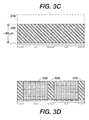
- FIGS. 3 A through 3D depict an assembly process of a fluidic membrane component in accordance with embodiments of the present teachings.
- Figure 4A is an exploded view and Figure 4B is an assembled view of a known print head structure.
- Embodiments pertain generally to MEMS inkjet print heads.
- the MEMS inkjet print head is a high speed, high density follow-on technology utilizing ink printing. More particularly, electrostatic micro-electro mechanical systems (“MEMS”) inkjet print heads can be configured to break off ink drops in a precise and controlled manner.
- MEMS micro-electro mechanical systems
- An electrostatic MEMS membrane and drive circuit can be fabricated using silicon wafer fabrication techniques, and are separately fabricated prior to integration into the print head.
- the exemplary structure and methods include integration of MEMS components with traditional microelectronic components such as CMOS drivers.
- Figure 1 A illustrates an exemplary exploded view of a MEMS inkjet print head 100 in accordance with an embodiment.
- Figure 1B illustrates an assembled view of the MEMS inkjet print head of Figure 1 A . It should be readily apparent to those of ordinary skill in the art that the MEMS inkjet print head 100 depicted in Figures 1 A and 1B represents a generalized schematic illustration and that other components may added or existing components may be removed or modified.
- the MEMS inkjet print head 100 depicted in Figures 1A and 1B includes a driver component 110, a fluid membrane component 112, and a nozzle plate 114. Each of these components can include further subcomponents as will be described herein.
- the MEMS inkjet print head 100 of the exemplary embodiments can be defined by a separately fabricated driver component 110 and membrane component 112, where the components are joined subsequent to their separate fabrications.
- a completed MEMS inkjet print head includes the nozzle plate 114 through which a liquid, such as ink or the like is dispensed.
- the driver component 110 includes a wafer substrate 116, a CMOS layer 118 on the substrate, a passivation dielectric 120 formed on the CMOS surface 118, a membrane electrode 122, ground potential electrode 123, and bonding features 124 formed on the passivation dielectric.
- the membrane component 112 includes, for example, an SOI wafer having a silicon wafer substrate 126, an oxide layer 128 formed on a surface of the substrate 126, and a device (membrane) layer 130 formed on the oxide layer 128.
- bonding features 132, 134 can be patterned on the device layer 130 for bonding with corresponding bonding features 124 of the driver component 110. As illustrated, the bonding features 132, 134 of the membrane component can be formed on a surface of the device layer 130 facing the bonding features 124 of the driver component 110.
- the nozzle plate 114 can be constructed as known in the art for dispensing drops of fluid in response to actuation of the membrane component 112 by the driver component 110.
- the nozzle plate 114 can have a plurality of apertures 115 formed therein for dispensing a fluid from the print head 100.
- a fluid such as ink (not shown) can be ejected from the apertures 115 in the nozzle plate 114.
- a drive signal is applied to the micro-electromechanical system (MEMS) membrane 130, it moves towards membrane electrode 122, decreasing the pressure in the ink cavity above and pulling ink into the cavity.
- the drive signal is turned off or decreased, the MEMS membrane 130 returns to its original position, increasing the pressure in the cavity above and causing ink to be ejected through apertures 115 in nozzle plate 114.
- MEMS micro-electromechanical system
- the driver component 110 is fabricated as illustrated by way of example in Figures 2A - 2E . Although a series of fabrication steps are described, it will be appreciated that various steps may be added or removed according to fabrication parameters. Further, although the driver component 110 is described particularly in connection with a CMOS device driver wafer, this is not intended to be limiting of the exemplary embodiments. Accordingly, the driver component 110 can also be built on a plain bare silicon or glass substrate.
- a silicon substrate wafer 216 is provided as a starting material for the driver component 110.
- a CMOS layer 218 is formed on a surface of the silicon substrate wafer 216. Depositing of the CMOS layer 218 can include multiple masks and layers as is known in the art.
- a passivation dielectric layer 220 is formed on the CMOS layer 218.
- the passivation layer 220 can be formed of silicon dioxide; however, this can be varied according to fabrication requirements.
- Other materials that can be used for passivation layer 220 can include silicon nitride, silicon dioxide with small amounts of nitrogen, and hafnium-based high-k dielectrics.
- an electrode 222 can be formed on the passivation dielectric 220.
- the electrode 222 forms the counterelectrode of a capacitive membrane (130 of Figures 1A and 1B ) of the membrane component 112 and can be recessed below bonding features 224 formed intermediate the electrodes 222.
- a membrane electrode can refer to a pattern of electrodes.
- a ground potential electrode 223 can be positioned intermediate the electrodes 222 in order correspond to or align with features of the membrane component 112 as will be described.
- the electrodes 222 can be doped polysilicon or any other conductor.
- the electrodes 222 can be aluminum, copper, ITO, or the like, and will be compatible with the base wafer processing. Previously, use of these types of electrodes was not thought to be possible since virtually all reactive metals are dissolvable in hydrofluoric acid. However, because the exemplary embodiments eliminate use of hydrofluoric acid etching and can incorporate the described metals, it is expected that the metal electrodes 222 can be applied directly to an upper surface of a microelectronic circuit, such as a CMOS driver array. One of ordinary skill in the art will understand suitable multi-level poly and metal processes applicable to the exemplary embodiments.
- bonding features 224 can be formed on a surface of the passivation dielectric.
- the electrodes 222 can be recessed below bonding features 224, thereby defining a gap height between the passivation dielectric 220 of the driver component 110 and the membrane component 112.
- the bonding features 224 can be patterned glass features applied before or after the electrode layer 222. It will be appreciated that the manufacturing process can vary according to process constraints and device design.
- the driver component 110 can also include a planar oxide or a surface that has been mechanically polished to provide a flat, uniform substrate surface.
- the mechanical polish can be, for example, a chemical mechanical polish (CMP) as known in the art.
- CMP chemical mechanical polish
- the planar oxide surface can be formed when the driver component 110 includes an oxide thereon. Since the driver component 110 can be separately fabricated from the membrane component 112, deposition of oxides can be tightly controlled and precise thicknesses can be achieved and maintained.
- the SOI wafer is depicted in Figure 3A and includes a silicon substrate 326, oxide layer 328 and device layer 330, assembled as known in the art.
- the device layer 330 can be a silicon device of about 2 ⁇ m thickness.
- the mating oxide layer 328 can be patterned to form a receiving oxide film 332 for wafer to wafer bonding on a surface of the device layer 328 facing the bonding features 224 of the driver component 110.
- This mating oxide layer can also be used to form an oxide dimple on the membrane 328 that could otherwise not be formed with traditional deposition methods.
- the dimple can be formed directly on the electrode 222 of Figures 2D , 2E .
- the device layer 330 can be, for example, the active layer of a SOI wafer. Although the thickness is not critical to an understanding of the embodiments, an active layer of about 2 ⁇ m can typically be used.
- the described structure is not limited to SOI wafer materials, and is further compatible with polysilicon membrane technology.
- polysilicon membrane technology a blank silicon wafer is used as a base. A suitable oxide is deposited and then a 2 ⁇ m (or desired thickness) of polysilicon is applied. Patterning and other depositions coincide with that described in connection with SOI.
- the device layer 330 can be optionally patterned since it remains exposed. This is an advantage not previously realized. In fact, by separately fabricating each of the driver component 110 and membrane component 112, and eliminating etching with hazardous materials such as hydrofluoric acid, many fabrication steps can be re-ordered to suit a particular design or foundry process.
- a thickness of the membrane component 112 can be defined by back-grinding and/or polishing the silicon handle layer 326 to a desired thickness. Grinding and/or polishing can occur in one or more steps either alternately or sequentially.
- a silicon handle layer 326 can be ground and/or polished to a thickness of about 80 ⁇ m.
- a deep etch can be performed on the silicon handle 326 and buried oxide layer 328 to expose the membrane layer 330.
- the deep etch results in the formation of fluid chambers 336 and fluid walls 338 surrounding the fluid chambers 338.
- the grinding, polishing and chamber etching can be performed prior to wafer bonding.
- the driver component 110 and membrane component 112 can be bonded followed by the grinding, polishing, and etching. It will be appreciated that the order of fabrication is not critical, and is instead flexible because of the separate fabrication of each of the driver component 110 and membrane component 112.
- the driver component 110 and the membrane component 112 can be bonded together with known wafer-to-wafer bonding techniques subsequent to their separate fabrication.
- the bonding features 224 of the driver component 110 are fusion bonded to the bonding features 332 of the membrane component 112.
- Wafer-to-wafer bonding is a very accurate method for joining wafers together.
- a glass fusion bond is extremely strong, hermetic, and accurate. No additional materials need to be added, nor is there any squeeze out in the bond area.
- This type of bond is particularly suitable for the exemplary embodiments as it can use materials that can already be found on the wafer, and are a natural fit to the process.
- the process and material used are currently supported in the semiconductor industry by existing equipment suppliers.
- glass fusion bond alternatives include gold diffusion bond, solder bond, adhesion bond, or the like.
- the completed print head 100 includes the nozzle plate 114 provided on an exposed surface of the membrane component 112 as illustrated in Figures 1A and 1B .
- the nozzle plate 114 is applied to an assembled driver substrate component 110 and fluidic membrane component 112 which can be previously bonded together by glass fusion as described above.
- the nozzle plate 114 can be applied at the point where the individual die are packaged into a print head array. This selection is architectural and not limited by the choices of wafer processing described herein.
Landscapes
- Engineering & Computer Science (AREA)
- Manufacturing & Machinery (AREA)
- Particle Formation And Scattering Control In Inkjet Printers (AREA)
- Micromachines (AREA)
Abstract
Description
- The present invention generally relates to integration of a driver substrate and a micro-electromechanical system (MEMS) membrane, and more particularly, integration of these components in a MEMS type inkjet print head.
- Heretofore, fabrication of a MEMS inkjet print head presented difficulties by virtue of the very components being joined. In particular, the MEMS inkjet print head incorporates a MEMS membrane device and a driver substrate, each formed with processes that can be detrimental to the other.
- Traditional MEMS membrane devices can be fabricated using thin film surface micromachining techniques. For example, polysilicon layers are deposited over sacrificial silicon glass layers and the sacrificial layers are dissolved through a multitude of etch holes to allow the etchant to flow underneath the membranes. This etch process can affect required passivation of microelectronic components and the required holes need to be hermetically sealed after the etch release in some cases to prevent the device from malfunctioning. The aggressive chemical etch is typically performed with hydrofluoric acid (HF), which limits material choices for the designer. Further, use of the chemical etch complicates an integration of MEMS devices with traditional microelectronic components such as a substrate driver used in the MEMS inkjet print head. In addition, released devices can be difficult to process with traditional microelectronic techniques creating yield loss or restricted design options.
- Conventional circuit driver substrates designed as CMOS devices are commonly employed to drive transducers and reduce input/output lines. These can be complex assemblies of thin films passivated with silicon oxides. If this type of device is exposed to a strong etchant, such as HF, it might no longer function. While steps can be taken to protect these passivation layers, other MEMS processes, particularly high temperature processes such as polysilicon deposition and annealing, can adversely impact the operation of transistor circuits. This is also aggravated by compound yield effects of additional microelectronic layers. Accordingly, CMOS and MEMS present a challenge to integrate.
-
Figures 4A and 4B depict some basic features of a known MEMS inkjet print head and are provided to illustrate differences between the known heads and that of the exemplary embodiments. - In the known polysilicon membrane design of a MEMS inkjet print head, a larger, more
complex structure 410 is used betweenadjacent membranes 420. These structures are used for sealing hydrofluoric acidetch release holes 430 in the membrane and for tolerance adjustments between membranes. In the exemplary embodiments described herein, a thinner, less complex fluid wall can be formed, and there are no holes in the membrane structure. - In order to form a print head device, the free membranes must be very small and at a very high density. For 600 nozzles per inch, the print head must have a pitch of 42.25 µm. This does not leave much room for sealing and alignment of the layers between each ejector nozzle.
- Thus, there is a need to overcome these and other problems of the prior art and to provide a method and apparatus for a MEMS electrostatic inkjet print head in which the electrostatic membrane and drive electrode are fabricated on separate wafers prior to bonding the wafers together in an inkjet print head.
- In accordance with the present teachings, a method of fabricating a MEMS inkjet type print head is provided.
- The exemplary method can include providing a driver component, separately providing an actuatable membrane component, the actuatable membrane component formed in the absence of an acid etch removing a sacrificial layer, bonding the separately provided actuatable membrane component to the driver component, and attaching a nozzle plate to the actuatable membrane component subsequent to the bonding.
In one embodiment of the method of claim 2, the electrodes comprise a conductor selected to be compatible with base wafer processing.
In a further embodiment the conductor comprises any of aluminum, copper, and indium tin oxide (ITO).
In a further embodiment the bonding features are silicon glass standoffs.
In a further embodiment the bonding features are applied to the driver component before the electrode layer.
In a further embodiment the bonding features are applied to the driver component after the electrode layer.
In a further embodiment acid etching comprises a hydrofluoric acid etch. - In accordance with the present teachings, a MEMS type inkjet print head is provided. The exemplary device can include a driver component and a MEMS component separately fabricated from the driver component, the MEMS component formed in the absence of an acid etch removing a sacrificial layer. Bonding features are provided to operatively join the driver component and the MEMS component, and a nozzle plate is attached to the MEMS component.
In a further embodiment the MEMS component formed in the absence of an acid etch removing a sacrificial layer.
In a further embodiment the aperture-free fluid membrane comprises silicon.
In a further embodiment the bonding features comprise glass.
In a further embodiment the driver component is manufactured with microelectronic methods. - It is to be understood that both the foregoing general description and the following detailed description are exemplary and explanatory only and are not restrictive of the invention, as claimed.
- The accompanying drawings, which are incorporated in and constitute a part of this specification, illustrate several embodiments of the invention and together with the description, serve to explain the principles of the invention.
-
Figure 1A depicts an exploded view of exemplary components of a print head assembly in accordance with embodiments of the present teachings; -
Figure 1B depicts an assembled print head in accordance with embodiments of the present teachings; -
Figures 2A through 2E depict an assembly process of a driver component in accordance with embodiments of the present teachings; -
Figures 3 A through 3D depict an assembly process of a fluidic membrane component in accordance with embodiments of the present teachings; and -
Figure 4A is an exploded view andFigure 4B is an assembled view of a known print head structure. - Reference will now be made in detail to the exemplary embodiments of the invention, examples of which are illustrated in the accompanying drawings. However, one of ordinary skill in the art would readily recognize that the same principles are equally applicable to, and can be implemented in devices other than inkjet printers, and that any such variations do not depart from the true spirit and scope of the present invention. Moreover, in the following detailed description, references are made to the accompanying figures, which illustrate specific embodiments. Electrical, mechanical, logical and structural changes may be made to the embodiments without departing from the spirit and scope of the present invention. The following detailed description is, therefore, not to be taken in a limiting sense and the scope of the present invention is defined by the appended claims and their equivalents. Wherever possible, the same reference numbers will be used throughout the drawings to refer to the same or like parts.
- Embodiments pertain generally to MEMS inkjet print heads. The MEMS inkjet print head is a high speed, high density follow-on technology utilizing ink printing. More particularly, electrostatic micro-electro mechanical systems ("MEMS") inkjet print heads can be configured to break off ink drops in a precise and controlled manner.
- An electrostatic MEMS membrane and drive circuit can be fabricated using silicon wafer fabrication techniques, and are separately fabricated prior to integration into the print head. The exemplary structure and methods include integration of MEMS components with traditional microelectronic components such as CMOS drivers.
-
Figure 1 A illustrates an exemplary exploded view of a MEMSinkjet print head 100 in accordance with an embodiment.Figure 1B illustrates an assembled view of the MEMS inkjet print head ofFigure 1 A . It should be readily apparent to those of ordinary skill in the art that the MEMSinkjet print head 100 depicted inFigures 1 A and 1B represents a generalized schematic illustration and that other components may added or existing components may be removed or modified. - The MEMS
inkjet print head 100 depicted inFigures 1A and 1B includes adriver component 110, afluid membrane component 112, and anozzle plate 114. Each of these components can include further subcomponents as will be described herein. - Essentially, the MEMS
inkjet print head 100 of the exemplary embodiments can be defined by a separately fabricateddriver component 110 andmembrane component 112, where the components are joined subsequent to their separate fabrications. A completed MEMS inkjet print head includes thenozzle plate 114 through which a liquid, such as ink or the like is dispensed. - As depicted in
Figures 1A and 1B , thedriver component 110 includes awafer substrate 116, aCMOS layer 118 on the substrate, apassivation dielectric 120 formed on theCMOS surface 118, amembrane electrode 122, groundpotential electrode 123, and bonding features 124 formed on the passivation dielectric. - The
membrane component 112 includes, for example, an SOI wafer having asilicon wafer substrate 126, anoxide layer 128 formed on a surface of thesubstrate 126, and a device (membrane)layer 130 formed on theoxide layer 128. In addition, bonding features 132, 134 can be patterned on thedevice layer 130 for bonding with corresponding bonding features 124 of thedriver component 110. As illustrated, the bonding features 132, 134 of the membrane component can be formed on a surface of thedevice layer 130 facing the bonding features 124 of thedriver component 110. - It will be appreciated that the
nozzle plate 114 can be constructed as known in the art for dispensing drops of fluid in response to actuation of themembrane component 112 by thedriver component 110. In particular, thenozzle plate 114 can have a plurality ofapertures 115 formed therein for dispensing a fluid from theprint head 100. - Turning now to the dispensing of fluid from the
nozzle plate 114 in the completedprint head 100, a fluid such as ink (not shown) can be ejected from theapertures 115 in thenozzle plate 114. When a drive signal is applied to the micro-electromechanical system (MEMS)membrane 130, it moves towardsmembrane electrode 122, decreasing the pressure in the ink cavity above and pulling ink into the cavity. When the drive signal is turned off or decreased, theMEMS membrane 130 returns to its original position, increasing the pressure in the cavity above and causing ink to be ejected throughapertures 115 innozzle plate 114. - The
driver component 110 is fabricated as illustrated by way of example inFigures 2A - 2E . Although a series of fabrication steps are described, it will be appreciated that various steps may be added or removed according to fabrication parameters. Further, although thedriver component 110 is described particularly in connection with a CMOS device driver wafer, this is not intended to be limiting of the exemplary embodiments. Accordingly, thedriver component 110 can also be built on a plain bare silicon or glass substrate. - As shown in
Figure 2A , asilicon substrate wafer 216 is provided as a starting material for thedriver component 110. InFigure 2B , aCMOS layer 218 is formed on a surface of thesilicon substrate wafer 216. Depositing of theCMOS layer 218 can include multiple masks and layers as is known in the art. InFigure 2C , apassivation dielectric layer 220 is formed on theCMOS layer 218. Typically, thepassivation layer 220 can be formed of silicon dioxide; however, this can be varied according to fabrication requirements. Other materials that can be used forpassivation layer 220 can include silicon nitride, silicon dioxide with small amounts of nitrogen, and hafnium-based high-k dielectrics. - As shown in
Figure 2D , anelectrode 222 can be formed on thepassivation dielectric 220. Theelectrode 222 forms the counterelectrode of a capacitive membrane (130 ofFigures 1A and 1B ) of themembrane component 112 and can be recessed below bonding features 224 formed intermediate theelectrodes 222. It will be appreciated that the term "a" membrane electrode can refer to a pattern of electrodes. For example, a groundpotential electrode 223 can be positioned intermediate theelectrodes 222 in order correspond to or align with features of themembrane component 112 as will be described. It will be appreciated that theelectrodes 222 can be doped polysilicon or any other conductor. For example, theelectrodes 222 can be aluminum, copper, ITO, or the like, and will be compatible with the base wafer processing. Previously, use of these types of electrodes was not thought to be possible since virtually all reactive metals are dissolvable in hydrofluoric acid. However, because the exemplary embodiments eliminate use of hydrofluoric acid etching and can incorporate the described metals, it is expected that themetal electrodes 222 can be applied directly to an upper surface of a microelectronic circuit, such as a CMOS driver array. One of ordinary skill in the art will understand suitable multi-level poly and metal processes applicable to the exemplary embodiments. - Referring to
Figure 2E , bonding features 224 can be formed on a surface of the passivation dielectric. Theelectrodes 222 can be recessed below bonding features 224, thereby defining a gap height between thepassivation dielectric 220 of thedriver component 110 and themembrane component 112. - The bonding features 224 can be patterned glass features applied before or after the
electrode layer 222. It will be appreciated that the manufacturing process can vary according to process constraints and device design. - The
driver component 110 can also include a planar oxide or a surface that has been mechanically polished to provide a flat, uniform substrate surface. The mechanical polish can be, for example, a chemical mechanical polish (CMP) as known in the art. Typically, the planar oxide surface can be formed when thedriver component 110 includes an oxide thereon. Since thedriver component 110 can be separately fabricated from themembrane component 112, deposition of oxides can be tightly controlled and precise thicknesses can be achieved and maintained. - Turning now to
Figures 3A - 3D , an exemplary fabrication of themembrane component 112 is depicted. The SOI wafer is depicted inFigure 3A and includes asilicon substrate 326,oxide layer 328 anddevice layer 330, assembled as known in the art. Thedevice layer 330 can be a silicon device of about 2 µm thickness. Themating oxide layer 328 can be patterned to form a receiving oxide film 332 for wafer to wafer bonding on a surface of thedevice layer 328 facing the bonding features 224 of thedriver component 110. This mating oxide layer can also be used to form an oxide dimple on themembrane 328 that could otherwise not be formed with traditional deposition methods. As an alternative, the dimple can be formed directly on theelectrode 222 ofFigures 2D ,2E . - The
device layer 330 can be, for example, the active layer of a SOI wafer. Although the thickness is not critical to an understanding of the embodiments, an active layer of about 2 µm can typically be used. - It will be appreciated that the described structure is not limited to SOI wafer materials, and is further compatible with polysilicon membrane technology. For polysilicon membrane technology, a blank silicon wafer is used as a base. A suitable oxide is deposited and then a 2 µm (or desired thickness) of polysilicon is applied. Patterning and other depositions coincide with that described in connection with SOI.
- Once the
device layer 330 is prepared for bonding, it can be optionally patterned since it remains exposed. This is an advantage not previously realized. In fact, by separately fabricating each of thedriver component 110 andmembrane component 112, and eliminating etching with hazardous materials such as hydrofluoric acid, many fabrication steps can be re-ordered to suit a particular design or foundry process. - As illustrated in
Figure 3C , a thickness of themembrane component 112 can be defined by back-grinding and/or polishing thesilicon handle layer 326 to a desired thickness. Grinding and/or polishing can occur in one or more steps either alternately or sequentially. By way of example, asilicon handle layer 326 can be ground and/or polished to a thickness of about 80 µm. - As depicted in
Figure 3D , a deep etch can be performed on thesilicon handle 326 and buriedoxide layer 328 to expose themembrane layer 330. The deep etch results in the formation offluid chambers 336 andfluid walls 338 surrounding thefluid chambers 338. - For deeper fluid chamber layers, the grinding, polishing and chamber etching can be performed prior to wafer bonding. For very thin fluid chamber layers or where the structure can become fragile due to its size, the
driver component 110 andmembrane component 112 can be bonded followed by the grinding, polishing, and etching. It will be appreciated that the order of fabrication is not critical, and is instead flexible because of the separate fabrication of each of thedriver component 110 andmembrane component 112. - The
driver component 110 and themembrane component 112 can be bonded together with known wafer-to-wafer bonding techniques subsequent to their separate fabrication. In the exemplary embodiments, the bonding features 224 of thedriver component 110 are fusion bonded to the bonding features 332 of themembrane component 112. Wafer-to-wafer bonding is a very accurate method for joining wafers together. A glass fusion bond is extremely strong, hermetic, and accurate. No additional materials need to be added, nor is there any squeeze out in the bond area. This type of bond is particularly suitable for the exemplary embodiments as it can use materials that can already be found on the wafer, and are a natural fit to the process. In addition, the process and material used are currently supported in the semiconductor industry by existing equipment suppliers. - Alternatives to glass fusion bond are acceptable for use in the exemplary embodiments and include gold diffusion bond, solder bond, adhesion bond, or the like.
- The completed
print head 100 includes thenozzle plate 114 provided on an exposed surface of themembrane component 112 as illustrated inFigures 1A and 1B . Typically, thenozzle plate 114 is applied to an assembleddriver substrate component 110 andfluidic membrane component 112 which can be previously bonded together by glass fusion as described above. As an option, thenozzle plate 114 can be applied at the point where the individual die are packaged into a print head array. This selection is architectural and not limited by the choices of wafer processing described herein. - It will be appreciated by those of skill in the art that the aggressive wet hydrofluoric acid etch is eliminated from the exemplary methods described herein, allowing combinations of layers that wouldn't otherwise be feasible. For example, when wet hydrofluoric acid etching is used, nitride films can be required to protect underlying oxides from inadvertent removal. In these types of membrane devices, high electric fields can be generated during operation. These nitride films can build up charge, changing the electric fields and resulting forces, and are therefore less than an ideal material. By eliminating the wet acid etching, options available to manufacturers become much more diverse. By way of example only, thermal oxides or other high quality dielectrics can now be utilized to improve the performance of the MEMS type inkjet print head without risk of damage to the component materials during processing.
- While the invention has been illustrated with respect to one or more exemplary embodiments, alterations and/or modifications can be made to the illustrated examples without departing from the spirit and scope of the appended claims. In particular, although the method has been described by examples, the steps of the method may be performed in a different order than illustrated or simultaneously. In addition, while a particular feature of the invention may have been disclosed with respect to only one of several embodiments, such feature may be combined with one or more other features of the other embodiments as may be desired and advantageous for any given or particular function. Furthermore, to the extent that the terms "including", "includes", "having", "has", "with", or variants thereof are used in either the detailed description and the claims, such terms are intended to be inclusive in a manner similar to the term "comprising." And as used herein, the term "one or more of" with respect to a listing of items such as, for example, "one or more of A and B," means A alone, B alone, or A and B.
- Notwithstanding that the numerical ranges and parameters setting forth the broad scope of the invention are approximations, the numerical values set forth in the specific examples are reported as precisely as possible. Any numerical value, however, inherently contains certain errors necessarily resulting from the standard deviation found in their respective testing measurements. Moreover, all ranges disclosed herein are to be understood to encompass any and all sub-ranges subsumed therein. For example, a range of "less than 10" can include any an all sub-ranges between (and including) the minimum value of zero and the maximum value of 10, that is, any and all sub-ranges having a minimum value of equal to or greater than zero and a maximum value of equal to or less than 10, e.g., 1 to 5.
Claims (10)
- A method of fabricating a MEMS inkjet type print head comprising:separately providing an actuatable membrane component, the actuatable membrane component formed in the absence of an acid etch removing a sacrificial layer;bonding the separately provided actuatable membrane component to the print head; andattaching a nozzle plate to the actuatable membrane component subsequent to the bonding.
- The method of claim 1, further providing a driver component, wherein the driver component is manufactured to include electrodes and bonding features on a surface of the driver component.
- The method of claim 1, wherein the bonding features include silicon glass standoffs.
- The method of claim 2, wherein the driver component is manufactured with microelectronic methods and further includes forming bonding features on a surface of the component.
- The method of claim 4, wherein the microelectronic methods include CMOS.
- The method of claim 2, wherein the driver component is built up from a CMOS device driver wafer.
- The method of claim 2, wherein the bonding features define a gap height between the driver component and the separately provided actuatable membrane component.
- The method of claim 2, wherein the electrodes are capacitive membrane electrodes.
- A MEMS type inkjet print head comprising:a driver component;a MEMS component separately fabricated from the driver component, the MEMS component including an aperture free fluid membrane;bonding features operatively joining the driver component and the MEMS component; anda nozzle plate attached to the MEMS component.
- A method of fabricating a MEMS inkjet type print head comprising:providing a driver component;separately providing an actuatable membrane component;bonding the separately provided actuatable membrane component to the driver component; andattaching a nozzle plate to the actuatable membrane component subsequent to the bonding.
Applications Claiming Priority (1)
| Application Number | Priority Date | Filing Date | Title |
|---|---|---|---|
| US11/693,209 US8455271B2 (en) | 2007-03-29 | 2007-03-29 | Highly integrated wafer bonded MEMS devices with release-free membrane manufacture for high density print heads |
Publications (2)
| Publication Number | Publication Date |
|---|---|
| EP1974922A1 true EP1974922A1 (en) | 2008-10-01 |
| EP1974922B1 EP1974922B1 (en) | 2013-05-15 |
Family
ID=39534843
Family Applications (1)
| Application Number | Title | Priority Date | Filing Date |
|---|---|---|---|
| EP08151995.1A Ceased EP1974922B1 (en) | 2007-03-29 | 2008-02-27 | Highly Integrated Wafer Bonded MEMS Devices with Release-Free Membrane Manufacture for High Density Print Heads |
Country Status (5)
| Country | Link |
|---|---|
| US (2) | US8455271B2 (en) |
| EP (1) | EP1974922B1 (en) |
| JP (1) | JP5356706B2 (en) |
| KR (1) | KR101497996B1 (en) |
| TW (1) | TWI427002B (en) |
Families Citing this family (6)
| Publication number | Priority date | Publication date | Assignee | Title |
|---|---|---|---|---|
| US8328331B2 (en) * | 2010-03-19 | 2012-12-11 | Xerox Corporation | Ink jet print head plate |
| US8789932B2 (en) * | 2010-05-27 | 2014-07-29 | Hewlett-Packard Development Company, L.P. | Printhead and related methods and systems |
| US8567913B2 (en) * | 2010-06-02 | 2013-10-29 | Xerox Corporation | Multiple priming holes for improved freeze/thaw cycling of MEMSjet printing devices |
| WO2012036103A1 (en) * | 2010-09-15 | 2012-03-22 | Ricoh Company, Ltd. | Electromechanical transducing device and manufacturing method thereof, and liquid droplet discharging head and liquid droplet discharging apparatus |
| US9096062B2 (en) * | 2011-08-01 | 2015-08-04 | Xerox Corporation | Manufacturing process for an ink jet printhead including a coverlay |
| US9421772B2 (en) | 2014-12-05 | 2016-08-23 | Xerox Corporation | Method of manufacturing ink jet printheads including electrostatic actuators |
Citations (2)
| Publication number | Priority date | Publication date | Assignee | Title |
|---|---|---|---|---|
| US6312108B1 (en) | 1998-08-07 | 2001-11-06 | Ricoh Company, Ltd. | Ink-jet head |
| EP1748500A2 (en) | 2005-07-25 | 2007-01-31 | Fuji Xerox Co., Ltd. | Piezoelectric element, droplet-ejecting head, and droplet-ejecting apparatus |
Family Cites Families (20)
| Publication number | Priority date | Publication date | Assignee | Title |
|---|---|---|---|---|
| JPH10157104A (en) * | 1996-11-28 | 1998-06-16 | Tec Corp | Ink jet printer head |
| US6648453B2 (en) * | 1997-07-15 | 2003-11-18 | Silverbrook Research Pty Ltd | Ink jet printhead chip with predetermined micro-electromechanical systems height |
| JP2001072073A (en) | 1999-08-31 | 2001-03-21 | Yoshino Kogyosho Co Ltd | Measuring tool |
| JP3796394B2 (en) * | 2000-06-21 | 2006-07-12 | キヤノン株式会社 | Method for manufacturing piezoelectric element and method for manufacturing liquid jet recording head |
| JP2002052705A (en) | 2000-08-04 | 2002-02-19 | Ricoh Co Ltd | INK JET HEAD, METHOD OF MANUFACTURING INK JET HEAD, AND IMAGE FORMING APPARATUS USING THE HEAD |
| JP4039799B2 (en) | 2000-11-06 | 2008-01-30 | 株式会社リコー | Droplet discharge head, image forming apparatus, and apparatus for discharging droplets |
| US6568794B2 (en) * | 2000-08-30 | 2003-05-27 | Ricoh Company, Ltd. | Ink-jet head, method of producing the same, and ink-jet printing system including the same |
| JP3963341B2 (en) | 2000-08-30 | 2007-08-22 | 株式会社リコー | Droplet discharge head |
| JP4070175B2 (en) | 2000-09-29 | 2008-04-02 | 株式会社リコー | Droplet ejection head, inkjet recording apparatus, image forming apparatus, and apparatus for ejecting droplets |
| US6705708B2 (en) * | 2001-02-09 | 2004-03-16 | Seiko Espon Corporation | Piezoelectric thin-film element, ink-jet head using the same, and method for manufacture thereof |
| JP4088817B2 (en) * | 2001-02-09 | 2008-05-21 | セイコーエプソン株式会社 | Method for manufacturing piezoelectric thin film element and ink jet head using the same |
| JP3828116B2 (en) * | 2003-01-31 | 2006-10-04 | キヤノン株式会社 | Piezoelectric element |
| JP3479530B2 (en) * | 2003-05-14 | 2003-12-15 | ブラザー工業株式会社 | Method of forming inkjet head |
| EP1680279B1 (en) * | 2003-10-10 | 2014-04-23 | Dimatix, Inc. | Print head with thin membrane |
| CN101080360B (en) * | 2004-10-21 | 2012-10-31 | 富士胶卷迪马蒂克斯股份有限公司 | Sacrificial substrate for etching |
| JP4654458B2 (en) * | 2004-12-24 | 2011-03-23 | リコープリンティングシステムズ株式会社 | Silicon member anodic bonding method, ink jet head manufacturing method using the same, ink jet head and ink jet recording apparatus using the same |
| JP4259509B2 (en) * | 2004-12-27 | 2009-04-30 | セイコーエプソン株式会社 | Electrostatic actuator, droplet discharge head, droplet discharge apparatus, electrostatic device, and manufacturing method thereof |
| JP2006187934A (en) | 2005-01-06 | 2006-07-20 | Seiko Epson Corp | Electrostatic actuator and manufacturing method thereof, droplet discharge head and manufacturing method thereof, droplet discharge apparatus and device |
| US7625073B2 (en) * | 2005-06-16 | 2009-12-01 | Canon Kabushiki Kaisha | Liquid discharge head and recording device |
| US7993969B2 (en) * | 2006-08-10 | 2011-08-09 | Infineon Technologies Ag | Method for producing a module with components stacked one above another |
-
2007
- 2007-03-29 US US11/693,209 patent/US8455271B2/en not_active Expired - Fee Related
-
2008
- 2008-02-27 EP EP08151995.1A patent/EP1974922B1/en not_active Ceased
- 2008-03-24 JP JP2008075885A patent/JP5356706B2/en not_active Expired - Fee Related
- 2008-03-28 KR KR1020080028749A patent/KR101497996B1/en not_active Expired - Fee Related
- 2008-03-28 TW TW097111259A patent/TWI427002B/en not_active IP Right Cessation
-
2013
- 2013-05-01 US US13/875,262 patent/US8828750B2/en not_active Expired - Fee Related
Patent Citations (2)
| Publication number | Priority date | Publication date | Assignee | Title |
|---|---|---|---|---|
| US6312108B1 (en) | 1998-08-07 | 2001-11-06 | Ricoh Company, Ltd. | Ink-jet head |
| EP1748500A2 (en) | 2005-07-25 | 2007-01-31 | Fuji Xerox Co., Ltd. | Piezoelectric element, droplet-ejecting head, and droplet-ejecting apparatus |
Also Published As
| Publication number | Publication date |
|---|---|
| EP1974922B1 (en) | 2013-05-15 |
| JP5356706B2 (en) | 2013-12-04 |
| US20080238997A1 (en) | 2008-10-02 |
| US8455271B2 (en) | 2013-06-04 |
| KR20080088484A (en) | 2008-10-02 |
| JP2008247031A (en) | 2008-10-16 |
| TWI427002B (en) | 2014-02-21 |
| US20130241999A1 (en) | 2013-09-19 |
| US8828750B2 (en) | 2014-09-09 |
| KR101497996B1 (en) | 2015-03-03 |
| TW200906634A (en) | 2009-02-16 |
Similar Documents
| Publication | Publication Date | Title |
|---|---|---|
| EP1321294B1 (en) | Piezoelectric ink-jet printhead and method for manufacturing the same | |
| US8828750B2 (en) | Highly integrated wafer bonded MEMS devices with release-free membrane manufacture for high density print heads | |
| EP1693206B1 (en) | Piezoelectric inkjet printhead and method of manufacturing the same | |
| US9362484B2 (en) | Forming a device having a curved piezoelectric membrane | |
| CN102741155B (en) | Structure manufacturing method and liquid discharge head substrate manufacturing method | |
| US8485639B2 (en) | Inkjet print head and method for manufacturing the same | |
| KR100682917B1 (en) | Piezoelectric inkjet printheads and manufacturing method thereof | |
| US8037605B2 (en) | Piezoelectric inkjet printhead and method of manufacturing the same | |
| US7585423B2 (en) | Liquid discharge head and producing method therefor | |
| KR100519760B1 (en) | Manufacturing method of piezoelectric ink-jet printhead | |
| US7585055B2 (en) | Integrated printhead with polymer structures | |
| JP2009119699A (en) | MASK SUBSTRATE, MANUFACTURING METHOD THEREOF, AND LIQUID DISCHARGE EJECTING HEAD | |
| JP2026085186A (en) | Liquid dispensing head and method for manufacturing a liquid dispensing head | |
| JP2002272144A (en) | Electrostatic actuator and inkjet head | |
| JP2008087444A (en) | Droplet ejector manufacturing method and droplet ejector | |
| KR20010045300A (en) | Method for manufacturing a nozzle part of an ink jetting apparatus |
Legal Events
| Date | Code | Title | Description |
|---|---|---|---|
| PUAI | Public reference made under article 153(3) epc to a published international application that has entered the european phase |
Free format text: ORIGINAL CODE: 0009012 |
|
| AK | Designated contracting states |
Kind code of ref document: A1 Designated state(s): AT BE BG CH CY CZ DE DK EE ES FI FR GB GR HR HU IE IS IT LI LT LU LV MC MT NL NO PL PT RO SE SI SK TR |
|
| AX | Request for extension of the european patent |
Extension state: AL BA MK RS |
|
| 17P | Request for examination filed |
Effective date: 20090401 |
|
| 17Q | First examination report despatched |
Effective date: 20090508 |
|
| AKX | Designation fees paid |
Designated state(s): DE FR GB |
|
| GRAP | Despatch of communication of intention to grant a patent |
Free format text: ORIGINAL CODE: EPIDOSNIGR1 |
|
| GRAS | Grant fee paid |
Free format text: ORIGINAL CODE: EPIDOSNIGR3 |
|
| GRAA | (expected) grant |
Free format text: ORIGINAL CODE: 0009210 |
|
| AK | Designated contracting states |
Kind code of ref document: B1 Designated state(s): DE FR GB |
|
| REG | Reference to a national code |
Ref country code: GB Ref legal event code: FG4D |
|
| REG | Reference to a national code |
Ref country code: DE Ref legal event code: R096 Ref document number: 602008024534 Country of ref document: DE Effective date: 20130711 |
|
| PLBE | No opposition filed within time limit |
Free format text: ORIGINAL CODE: 0009261 |
|
| STAA | Information on the status of an ep patent application or granted ep patent |
Free format text: STATUS: NO OPPOSITION FILED WITHIN TIME LIMIT |
|
| 26N | No opposition filed |
Effective date: 20140218 |
|
| REG | Reference to a national code |
Ref country code: DE Ref legal event code: R097 Ref document number: 602008024534 Country of ref document: DE Effective date: 20140218 |
|
| REG | Reference to a national code |
Ref country code: FR Ref legal event code: PLFP Year of fee payment: 9 |
|
| REG | Reference to a national code |
Ref country code: FR Ref legal event code: PLFP Year of fee payment: 10 |
|
| REG | Reference to a national code |
Ref country code: FR Ref legal event code: PLFP Year of fee payment: 11 |
|
| PGFP | Annual fee paid to national office [announced via postgrant information from national office to epo] |
Ref country code: GB Payment date: 20200123 Year of fee payment: 13 Ref country code: DE Payment date: 20200121 Year of fee payment: 13 |
|
| PGFP | Annual fee paid to national office [announced via postgrant information from national office to epo] |
Ref country code: FR Payment date: 20200122 Year of fee payment: 13 |
|
| REG | Reference to a national code |
Ref country code: DE Ref legal event code: R119 Ref document number: 602008024534 Country of ref document: DE |
|
| GBPC | Gb: european patent ceased through non-payment of renewal fee |
Effective date: 20210227 |
|
| PG25 | Lapsed in a contracting state [announced via postgrant information from national office to epo] |
Ref country code: DE Free format text: LAPSE BECAUSE OF NON-PAYMENT OF DUE FEES Effective date: 20210901 Ref country code: FR Free format text: LAPSE BECAUSE OF NON-PAYMENT OF DUE FEES Effective date: 20210228 Ref country code: GB Free format text: LAPSE BECAUSE OF NON-PAYMENT OF DUE FEES Effective date: 20210227 |