EP1973193A1 - Mehrbandantennenvorrichtung, parasitäres Element und Kommunikationsvorrichtung - Google Patents
Mehrbandantennenvorrichtung, parasitäres Element und Kommunikationsvorrichtung Download PDFInfo
- Publication number
- EP1973193A1 EP1973193A1 EP07445010A EP07445010A EP1973193A1 EP 1973193 A1 EP1973193 A1 EP 1973193A1 EP 07445010 A EP07445010 A EP 07445010A EP 07445010 A EP07445010 A EP 07445010A EP 1973193 A1 EP1973193 A1 EP 1973193A1
- Authority
- EP
- European Patent Office
- Prior art keywords
- parasitic element
- antenna device
- parasitic
- communication device
- slit
- Prior art date
- Legal status (The legal status is an assumption and is not a legal conclusion. Google has not performed a legal analysis and makes no representation as to the accuracy of the status listed.)
- Granted
Links
Images

Classifications
-
- H—ELECTRICITY
- H01—ELECTRIC ELEMENTS
- H01Q—ANTENNAS, i.e. RADIO AERIALS
- H01Q1/00—Details of, or arrangements associated with, antennas
- H01Q1/12—Supports; Mounting means
- H01Q1/22—Supports; Mounting means by structural association with other equipment or articles
- H01Q1/24—Supports; Mounting means by structural association with other equipment or articles with receiving set
- H01Q1/241—Supports; Mounting means by structural association with other equipment or articles with receiving set used in mobile communications, e.g. GSM
- H01Q1/242—Supports; Mounting means by structural association with other equipment or articles with receiving set used in mobile communications, e.g. GSM specially adapted for hand-held use
- H01Q1/243—Supports; Mounting means by structural association with other equipment or articles with receiving set used in mobile communications, e.g. GSM specially adapted for hand-held use with built-in antennas
-
- H—ELECTRICITY
- H01—ELECTRIC ELEMENTS
- H01Q—ANTENNAS, i.e. RADIO AERIALS
- H01Q5/00—Arrangements for simultaneous operation of antennas on two or more different wavebands, e.g. dual-band or multi-band arrangements
- H01Q5/30—Arrangements for providing operation on different wavebands
- H01Q5/378—Combination of fed elements with parasitic elements
- H01Q5/392—Combination of fed elements with parasitic elements the parasitic elements having dual-band or multi-band characteristics
-
- H—ELECTRICITY
- H01—ELECTRIC ELEMENTS
- H01Q—ANTENNAS, i.e. RADIO AERIALS
- H01Q9/00—Electrically-short antennas having dimensions not more than twice the operating wavelength and consisting of conductive active radiating elements
- H01Q9/04—Resonant antennas
- H01Q9/0407—Substantially flat resonant element parallel to ground plane, e.g. patch antenna
- H01Q9/0421—Substantially flat resonant element parallel to ground plane, e.g. patch antenna with a shorting wall or a shorting pin at one end of the element
-
- H—ELECTRICITY
- H01—ELECTRIC ELEMENTS
- H01Q—ANTENNAS, i.e. RADIO AERIALS
- H01Q9/00—Electrically-short antennas having dimensions not more than twice the operating wavelength and consisting of conductive active radiating elements
- H01Q9/04—Resonant antennas
- H01Q9/0407—Substantially flat resonant element parallel to ground plane, e.g. patch antenna
- H01Q9/0442—Substantially flat resonant element parallel to ground plane, e.g. patch antenna with particular tuning means
-
- H—ELECTRICITY
- H01—ELECTRIC ELEMENTS
- H01Q—ANTENNAS, i.e. RADIO AERIALS
- H01Q9/00—Electrically-short antennas having dimensions not more than twice the operating wavelength and consisting of conductive active radiating elements
- H01Q9/04—Resonant antennas
- H01Q9/0407—Substantially flat resonant element parallel to ground plane, e.g. patch antenna
- H01Q9/0464—Annular ring patch
Definitions
- the invention relates to the field of antennas, and in particular to microstrip antennas comprising a driven element and a parasitic element.
- the invention also relates to a parasitic element and to a communication device comprising such antenna device.
- Antennas constitute a crucial part of such wireless communication system, and there is a corresponding desire to reduce their cost and size.
- the physical size of an antenna is not as much related to the improvements of the manufacturing methods used, as to the operating frequency or wavelength of the system in which it is to be used. Accordingly, as portable devices, such as mobile phones, become smaller and smaller, new requirements are placed on miniaturizing the antennas to be used within such devices as well.
- the bandwidth of an antenna is the range of frequencies over which it is effective, usually centred around the resonance frequency.
- the bandwidth of an antenna is an important aspect in antenna design, and may be increased by several techniques. For example, multiple antennas can be combined into a single assembly and allowing the natural impedance to select the correct antenna.
- Another way to improve the bandwidth for a specific resonance frequency is to use a parasitic element, an example being the use of a planar inverted F antenna (PIFA) with a parasitic element.
- PIFA planar inverted F antenna
- such a solution requires multiple parasitic elements, which in turn increases the size of the antenna device.
- Another object is to provide a radio communication device comprising such an antenna device.
- an antenna device suitable for a communication device operable in at least two frequency intervals.
- the antenna device comprises a generally planar driven radiating element having a feeding point connectable to a feed device of the communication device.
- the antenna device further comprises a generally planar parasitic element having a grounding portion connectable to a ground device of the communication device.
- the driven radiating element and the parasitic element are essentially coplanar and separated by a gap.
- the parasitic element of the invention comprises a slit, by means of which a double-resonance is provided in a first frequency interval of the frequency intervals in which the communication device is operable.
- an increased bandwidth is provided by means of the parasitic element, without the drawbacks of using several separate parasitic elements.
- the inventive antenna device provides a more space efficient solution than known devices. Further, the inventive antenna device does not require separate groundings for the different parasitic elements. This feature, besides again providing a more space efficient solution, minimizes the manufacturing and assembly costs.
- the parasitic element comprises one or more slits arranged in different ways.
- the invention thus provides a flexible antenna device, which may easily be adapted for use in different communication devices.
- the double-resonance can for example be provided in a lower frequency interval, in a higher frequency interval or in both the lower and the higher frequency intervals.
- the antenna device is arranged in a novel way.
- the antenna device is arranged with the driven radiating element arranged closest to the upper part of the communication device and the parasitic element surrounding the driven radiating element on the lower and vertical sides thereof. Improved radiation patterns are thereby obtained.
- the invention also relates to a radio communication device comprising such an antenna device whereby advantages similar to the above are achieved.
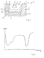
- FIG. 1 illustrates an antenna device in accordance with an embodiment of the invention.
- the antenna device 1 comprises a first radiating element 2, which is an active element, also known as a driven element, and in the following denoted driven radiating element 2.
- the driven radiating element 2 is made of a suitable electrically conductive material, such as a metal sheet, or a conductive flex film or the like.
- the driven radiating element 2 may have any suitable shape, for example square, rectangular, thin strip, circular, elliptical or triangular.
- the driven radiating element 2 is connected to a feed portion electrically connectable to radio frequency (RF) circuitry of an underlying printed circuit board (PCB) of a communication device in which the antenna device 1 is to be used.
- the feed portion could be a contact pin 5 having an extension essentially perpendicular to the plane of the driven radiating element 2.
- a contact pin 5 is used as an exemplary feed means, although it is noted that other feeding means could be used.
- the contact pin 5 functions as a feeding point of the driven radiating element 2.
- the contact pin 5 is preferably, but not necessarily, located on the edge of an opening or aperture 4 in the central part of the driven radiating element 2.
- the driven radiating element 2 is thus fed via the contact pin 5.
- the aperture 4 is used in order to increase the electrical size of the patch antenna.
- the PCB of the communication device also functions as a ground plane for the internal antenna device 1, in the described embodiments a modified patch antenna.
- the antenna device 1 further comprises a parasitic element 3.
- the parasitic element 3 is, like the driven radiating element 2, made of a suitable electrically conductive material.
- the parasitic element 3 is connected to a grounding portion, indicated in the figure at G.
- the parasitic element 3 has a general shape resembling a "C" turned 90 degrees counter-clockwise. That is, the parasitic element 3 comprises two parallel planar portions.
- the two parallel planar portions of the parasitic element 3 are indicated as portions A, B surrounded by dashed lines.
- the two parallel planar portions A, B are interconnected by means of a third planar portion C, also surrounded by dashed lines for illustration.
- the planar portion C is thus perpendicular to the two parallel planar portions A, B.
- the parasitic element 3 is preferably made in a single piece, for example stamped out from a suitable material.
- the shape of the parasitic element 3 can thereby be made to conform to the shape of the driven radiating element 2 when the driven radiating element 2 has a rectangular or square shape.
- the parasitic element 3 thus partially surrounds the driven radiating element 2 on three of the four sides of the driven radiating element 2. Stated differently, the parasitic element 3 is arranged along three sides of the driven radiating element 2. There is a gap 7 between the driven radiating element 2 and the parasitic element 3.
- the driven radiating element 2 and the parasitic element 3 are supported by a frame made of a non-conductive material, such as plastic (not shown). By means of the frame the radiating elements 2, 3 are easily positioned essentially parallel to the PCB of the communication device.
- the antenna device 1 is a multi-band antenna.
- the driven radiating element 2 and the parasitic element 3 can be dimensioned in order to obtain any desired resonance frequencies.
- the antenna device 1 may for example be dimensioned so as to produce a resonance at the lower bands with central frequencies substantially at 850 MHz and 900 MHz and/or to produce a resonance at the higher frequency bands with central frequencies substantially at 1800 MHz, 1900 MHz or 2100 MHz, making it suitable for use in a multi-band communication device adapted for the GSM850, GSM900 and/or GSM1800/GSM1900/WCDMA2100 bands.
- the capacitive coupling between the driven radiating element 2 and the parasitic element 3 can be used for determining the characteristics of the antenna device 1.
- the shape of the driven radiating element 2 can be adjusted in a controlled way in order to obtain the desired antenna characteristics.
- the width of the gap 7 between the driven radiating element 2 and the parasitic element 3 can be altered; if, for example, the width of the driven radiating element 2 is decreased, then the size of the gap 7 between the radiating driven element 2 and the parasitic element 3 is increased and thereby the resonance frequency of an upper band is lowered.
- the size of the slit 6 also affects the antenna characteristics.
- the width of the gap 7 lying closest to part C controls the resonance frequencies for both the upper and lower frequency bands.
- the parasitic element 3 is slitted or branched.
- the slit is indicated at reference numeral 6.
- the parasitic element 3 comprises frequency specific branches 3a, 3b, 3c originating from the grounding portion G, or from a common branch of the parasitic element 3.
- Providing the parasitic element 3 with a slit 6 as shown in the figure enables a double-resonance for the lower frequency band. For example, resonance frequencies of 850 MHz and 900 MHz may be provided in the lower frequency band.
- the resonance frequencies of the parasitic element 3 are dependent on the interrelation of the dimensions of the element branches 3a, 3b, 3c.
- the parasitic element 3 can be used to widen one or several of the operating frequency bands.
- the resonating frequencies of the driven radiating element 2 and the parasitic element branches 3a, 3b, 3c are then made somewhat different, in a manner know as such. Due care should be taken so that the matching of the antenna device 1 remains good enough over the whole range between the resonating frequencies.
- FIG. 2 illustrates schematically curves representing voltage standing wave ration (VSWR) as a function of frequency.
- VSWR voltage standing wave ration
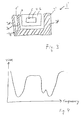
- Figure 3 illustrates another embodiment of the parasitic element of the antenna device 1'.
- same reference numerals are used as in figure 1 , for denoting same elements.
- the slit 6' of the parasitic element 3' in this embodiment is arranged at the other, higher frequency band, thereby providing a double-resonance at the higher frequency band interval instead.
- Figure 4 is similar to figure 2 , and illustrates schematically curves representing VSWR as a function of frequency.
- the resonance frequencies obtained in the higher frequency band by means of the antenna device 1' shown in figure 3 is indicated schematically. Again, specific frequencies are not indicated in the figure.
- Figure 5 illustrates schematically yet another embodiment of the invention.
- the parasitic element 3" of the antenna device 1" is provided with two slits 6 1 ", 6 2 ".
- One slit 6 1 " is arranged at the higher frequency band, thereby providing a double-resonance at the higher frequency band interval.
- the other slit 6 2 " is arranged at the lower frequency band, thereby providing a double-resonance at the lower frequency band interval.
- Figure 6 is similar to figures 2 and 4 , and illustrates schematically curves representing VSWR as a function of frequency.
- the resonance frequencies obtained in the higher and lower frequency bands by means of the antenna device 1" shown in figure 5 is indicated schematically. Again, specific frequencies are not indicated in the figure.
- the parasitic element of the invention can be provided with further additional slits in order to provide further resonance frequencies.
- additional slits are made at the cost of an increased space requirement.
- An advantage of the parasitic element 3, 3', 3" is that the different parasitic branches 3a, 3b, 3c, 3d, 3e, 3f do not require separate groundings portions.
- the number of contact points between the PCB of the communication device to which the antenna device 1 is to be connected and the antenna device 1 can thereby be minimized. This gives a less expensive manufacturing since the assembly is facilitated.
- the bandwidth can be increased by at least 30% compared to using a conventional, non-slitted parasitic element.
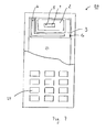
- the invention is also related to a communication device 20 comprising the antenna device 1 as described above.
- the communication device 20 for example a second generation or third generation cellular phone, comprises a keypad 24, display and other conventional means.
- a printed circuit board (PCB) 26 Inside the communication device 20 there is provided a printed circuit board (PCB) 26 with a size essentially corresponding to the size of the communication device 20.
- PCB 26 On the PCB 26 there are mounted electronic circuits etc. (not shown) for the operation of the communication device 20. These circuits are generally not part of the present invention and will not be discussed further.
- the antenna device is to be connected to the PCB and the PCB 26 comprises radio frequency (RF) circuitry for operation of the antenna device.
- RF radio frequency
- the parasitic element 3 is connected to the grounding portion G extending essentially perpendicular thereto.
- the grounding portion G is connected to a ground device of the underlying PCB 26.
- the driven radiating element 2 is electrically connected to a feed device of the PCB 26 by means of the contact pin 5.
- the antenna device 1 is shown to be arranged on the PCB 26 with the driven radiating element 2 closest to the upper part of the communication device 20 and the parasitic element 3 partially surrounding the driven radiating element 2 on the lower and vertical sides thereof. That is, the parasitic element 3 is arranged along three sides of the driven radiating element 2, wherein the lower side of it (i.e. the part denoted C in figure 1 ) is arranged closest to the key pad 24 and wherein the parallel parts (i.e. parts A and B in figure 1 ) are pointing upward, i.e. towards the upper part of the communication device 20. It has been found that such placement provides optimized radiation patterns as compared to turning the antenna device 180°, which is the typical way of arranging the antenna device.
- the invention has been described by means of different embodiments thereof. It is to be noted that the invention can be modified in a number of ways.
- the size of the grounding portion G can be used as a parameter when adjusting the characteristics of the antenna device 1.
- the grounding portion G may further be located differently than shown in the figures.
- the term radiating element should be understood to cover any antenna element adapted to receive or transmit electromagnetic waves.
Landscapes
- Engineering & Computer Science (AREA)
- Computer Networks & Wireless Communication (AREA)
- Waveguide Aerials (AREA)
- Details Of Aerials (AREA)
- Support Of Aerials (AREA)
Priority Applications (1)
| Application Number | Priority Date | Filing Date | Title |
|---|---|---|---|
| EP07445010A EP1973193B1 (de) | 2007-03-21 | 2007-03-21 | Mehrbandantennenvorrichtung, parasitäres Element und Kommunikationsvorrichtung |
Applications Claiming Priority (1)
| Application Number | Priority Date | Filing Date | Title |
|---|---|---|---|
| EP07445010A EP1973193B1 (de) | 2007-03-21 | 2007-03-21 | Mehrbandantennenvorrichtung, parasitäres Element und Kommunikationsvorrichtung |
Publications (2)
| Publication Number | Publication Date |
|---|---|
| EP1973193A1 true EP1973193A1 (de) | 2008-09-24 |
| EP1973193B1 EP1973193B1 (de) | 2012-10-17 |
Family
ID=38330458
Family Applications (1)
| Application Number | Title | Priority Date | Filing Date |
|---|---|---|---|
| EP07445010A Expired - Fee Related EP1973193B1 (de) | 2007-03-21 | 2007-03-21 | Mehrbandantennenvorrichtung, parasitäres Element und Kommunikationsvorrichtung |
Country Status (1)
| Country | Link |
|---|---|
| EP (1) | EP1973193B1 (de) |
Cited By (3)
| Publication number | Priority date | Publication date | Assignee | Title |
|---|---|---|---|---|
| CN107689485A (zh) * | 2016-08-04 | 2018-02-13 | 泰连公司 | 具有带寄生元件的多频带缝隙天线的无线通信装置 |
| DE102019205556A1 (de) * | 2019-04-17 | 2020-10-22 | BSH Hausgeräte GmbH | Leiterplatten-Antenne |
| CN112448147A (zh) * | 2019-08-29 | 2021-03-05 | 上海诺基亚贝尔股份有限公司 | 一种环贴片天线 |
Families Citing this family (1)
| Publication number | Priority date | Publication date | Assignee | Title |
|---|---|---|---|---|
| GB2571279B (en) | 2018-02-21 | 2022-03-09 | Pet Tech Limited | Antenna arrangement and associated method |
Citations (4)
| Publication number | Priority date | Publication date | Assignee | Title |
|---|---|---|---|---|
| US20030122718A1 (en) | 2001-12-27 | 2003-07-03 | Shyh-Tirng Fang | Dual-frequency planar antenna |
| EP1538703A1 (de) | 2003-06-09 | 2005-06-08 | Matsushita Electric Industrial Co., Ltd. | Antenne und elektronisches gerät |
| EP1703587A1 (de) | 2004-04-27 | 2006-09-20 | Murata Manufacturing Co., Ltd. | Antenne und tragbare funkkommunikationseinheit |
| US20060227052A1 (en) | 2005-04-07 | 2006-10-12 | X-Ether, Inc. | Multi-band or wide-band antenna |
-
2007
- 2007-03-21 EP EP07445010A patent/EP1973193B1/de not_active Expired - Fee Related
Patent Citations (4)
| Publication number | Priority date | Publication date | Assignee | Title |
|---|---|---|---|---|
| US20030122718A1 (en) | 2001-12-27 | 2003-07-03 | Shyh-Tirng Fang | Dual-frequency planar antenna |
| EP1538703A1 (de) | 2003-06-09 | 2005-06-08 | Matsushita Electric Industrial Co., Ltd. | Antenne und elektronisches gerät |
| EP1703587A1 (de) | 2004-04-27 | 2006-09-20 | Murata Manufacturing Co., Ltd. | Antenne und tragbare funkkommunikationseinheit |
| US20060227052A1 (en) | 2005-04-07 | 2006-10-12 | X-Ether, Inc. | Multi-band or wide-band antenna |
Cited By (4)
| Publication number | Priority date | Publication date | Assignee | Title |
|---|---|---|---|---|
| CN107689485A (zh) * | 2016-08-04 | 2018-02-13 | 泰连公司 | 具有带寄生元件的多频带缝隙天线的无线通信装置 |
| DE102019205556A1 (de) * | 2019-04-17 | 2020-10-22 | BSH Hausgeräte GmbH | Leiterplatten-Antenne |
| CN112448147A (zh) * | 2019-08-29 | 2021-03-05 | 上海诺基亚贝尔股份有限公司 | 一种环贴片天线 |
| CN112448147B (zh) * | 2019-08-29 | 2022-12-27 | 上海诺基亚贝尔股份有限公司 | 一种环贴片天线 |
Also Published As
| Publication number | Publication date |
|---|---|
| EP1973193B1 (de) | 2012-10-17 |
Similar Documents
| Publication | Publication Date | Title |
|---|---|---|
| US6573869B2 (en) | Multiband PIFA antenna for portable devices | |
| US6963308B2 (en) | Multiband antenna | |
| EP1451899B1 (de) | Kompakte breitbandantenne | |
| US6980154B2 (en) | Planar inverted F antennas including current nulls between feed and ground couplings and related communications devices | |
| US6714162B1 (en) | Narrow width dual/tri ISM band PIFA for wireless applications | |
| US7564413B2 (en) | Multi-band antenna and mobile communication terminal having the same | |
| JP3864127B2 (ja) | デュアルフィーディングポートを有するマルチバンドチップアンテナ及びこれを用いる移動通信装置 | |
| US7605766B2 (en) | Multi-band antenna device for radio communication terminal and radio communication terminal comprising the multi-band antenna device | |
| US7209087B2 (en) | Mobile phone antenna | |
| US20100060528A1 (en) | Dual-frequency antenna | |
| EP1128466A2 (de) | Planare Antennenstruktur | |
| EP2375489A2 (de) | Mobiles drahtloses Endgerät und Antennenvorrichtung | |
| EP2575207B1 (de) | Elektronisches Kommunikationsgerät und Antennenstruktur dafür | |
| US7095371B2 (en) | Antenna assembly | |
| EP2381529B1 (de) | Kommunikationsstrukturen mit Antennen mit separaten Antennenzweigen, die gekoppelt werden, um Leiter zu speisen und erden | |
| US20050017912A1 (en) | Dual-access monopole antenna assembly | |
| EP2610967B1 (de) | Kommunikationsvorrichtung und Antennenstruktur darin | |
| JP2011528520A (ja) | アンテナ装置 | |
| EP2019448A1 (de) | Antennenvorrichtung | |
| Kwak et al. | A folded planar inverted-F antenna for GSM/DCS/Bluetooth triple-band application | |
| US7106254B2 (en) | Single-mode antenna assembly | |
| EP1973193B1 (de) | Mehrbandantennenvorrichtung, parasitäres Element und Kommunikationsvorrichtung | |
| US10418709B1 (en) | Planar inverted F-antenna | |
| KR100723682B1 (ko) | 단말기용 삼중대역 cpw급전 평면 역f형 안테나 | |
| US20130099978A1 (en) | Internal printed antenna |
Legal Events
| Date | Code | Title | Description |
|---|---|---|---|
| PUAI | Public reference made under article 153(3) epc to a published international application that has entered the european phase |
Free format text: ORIGINAL CODE: 0009012 |
|
| AK | Designated contracting states |
Kind code of ref document: A1 Designated state(s): AT BE BG CH CY CZ DE DK EE ES FI FR GB GR HU IE IS IT LI LT LU LV MC MT NL PL PT RO SE SI SK TR |
|
| AX | Request for extension of the european patent |
Extension state: AL BA HR MK RS |
|
| 17P | Request for examination filed |
Effective date: 20090316 |
|
| 17Q | First examination report despatched |
Effective date: 20090421 |
|
| AKX | Designation fees paid |
Designated state(s): DE FI FR |
|
| GRAP | Despatch of communication of intention to grant a patent |
Free format text: ORIGINAL CODE: EPIDOSNIGR1 |
|
| GRAS | Grant fee paid |
Free format text: ORIGINAL CODE: EPIDOSNIGR3 |
|
| GRAA | (expected) grant |
Free format text: ORIGINAL CODE: 0009210 |
|
| AK | Designated contracting states |
Kind code of ref document: B1 Designated state(s): DE FI FR |
|
| REG | Reference to a national code |
Ref country code: DE Ref legal event code: R096 Ref document number: 602007026114 Country of ref document: DE Effective date: 20121213 |
|
| PG25 | Lapsed in a contracting state [announced via postgrant information from national office to epo] |
Ref country code: FI Free format text: LAPSE BECAUSE OF FAILURE TO SUBMIT A TRANSLATION OF THE DESCRIPTION OR TO PAY THE FEE WITHIN THE PRESCRIBED TIME-LIMIT Effective date: 20121017 |
|
| PGFP | Annual fee paid to national office [announced via postgrant information from national office to epo] |
Ref country code: DE Payment date: 20130322 Year of fee payment: 7 |
|
| PLBE | No opposition filed within time limit |
Free format text: ORIGINAL CODE: 0009261 |
|
| STAA | Information on the status of an ep patent application or granted ep patent |
Free format text: STATUS: NO OPPOSITION FILED WITHIN TIME LIMIT |
|
| 26N | No opposition filed |
Effective date: 20130718 |
|
| REG | Reference to a national code |
Ref country code: DE Ref legal event code: R097 Ref document number: 602007026114 Country of ref document: DE Effective date: 20130718 |
|
| REG | Reference to a national code |
Ref country code: FR Ref legal event code: ST Effective date: 20131129 |
|
| PG25 | Lapsed in a contracting state [announced via postgrant information from national office to epo] |
Ref country code: FR Free format text: LAPSE BECAUSE OF NON-PAYMENT OF DUE FEES Effective date: 20130402 |
|
| REG | Reference to a national code |
Ref country code: DE Ref legal event code: R119 Ref document number: 602007026114 Country of ref document: DE |
|
| REG | Reference to a national code |
Ref country code: DE Ref legal event code: R119 Ref document number: 602007026114 Country of ref document: DE Effective date: 20141001 |
|
| PG25 | Lapsed in a contracting state [announced via postgrant information from national office to epo] |
Ref country code: DE Free format text: LAPSE BECAUSE OF NON-PAYMENT OF DUE FEES Effective date: 20141001 |