EP1970943A1 - Optical integrator, illumination optical device, aligner, and method for fabricating device - Google Patents
Optical integrator, illumination optical device, aligner, and method for fabricating device Download PDFInfo
- Publication number
- EP1970943A1 EP1970943A1 EP06823415A EP06823415A EP1970943A1 EP 1970943 A1 EP1970943 A1 EP 1970943A1 EP 06823415 A EP06823415 A EP 06823415A EP 06823415 A EP06823415 A EP 06823415A EP 1970943 A1 EP1970943 A1 EP 1970943A1
- Authority
- EP
- European Patent Office
- Prior art keywords
- surface regions
- refracting surface
- regions
- optical integrator
- optical
- Prior art date
- Legal status (The legal status is an assumption and is not a legal conclusion. Google has not performed a legal analysis and makes no representation as to the accuracy of the status listed.)
- Withdrawn
Links
Images








Classifications
-
- G—PHYSICS
- G02—OPTICS
- G02B—OPTICAL ELEMENTS, SYSTEMS OR APPARATUS
- G02B27/00—Optical systems or apparatus not provided for by any of the groups G02B1/00 - G02B26/00, G02B30/00
- G02B27/10—Beam splitting or combining systems
-
- G—PHYSICS
- G02—OPTICS
- G02B—OPTICAL ELEMENTS, SYSTEMS OR APPARATUS
- G02B3/00—Simple or compound lenses
- G02B3/0006—Arrays
- G02B3/0037—Arrays characterized by the distribution or form of lenses
- G02B3/0062—Stacked lens arrays, i.e. refractive surfaces arranged in at least two planes, without structurally separate optical elements in-between
- G02B3/0068—Stacked lens arrays, i.e. refractive surfaces arranged in at least two planes, without structurally separate optical elements in-between arranged in a single integral body or plate, e.g. laminates or hybrid structures with other optical elements
-
- G—PHYSICS
- G03—PHOTOGRAPHY; CINEMATOGRAPHY; ANALOGOUS TECHNIQUES USING WAVES OTHER THAN OPTICAL WAVES; ELECTROGRAPHY; HOLOGRAPHY
- G03F—PHOTOMECHANICAL PRODUCTION OF TEXTURED OR PATTERNED SURFACES, e.g. FOR PRINTING, FOR PROCESSING OF SEMICONDUCTOR DEVICES; MATERIALS THEREFOR; ORIGINALS THEREFOR; APPARATUS SPECIALLY ADAPTED THEREFOR
- G03F7/00—Photomechanical, e.g. photolithographic, production of textured or patterned surfaces, e.g. printing surfaces; Materials therefor, e.g. comprising photoresists; Apparatus specially adapted therefor
- G03F7/70—Microphotolithographic exposure; Apparatus therefor
- G03F7/70058—Mask illumination systems
- G03F7/70075—Homogenization of illumination intensity in the mask plane by using an integrator, e.g. fly's eye lens, facet mirror or glass rod, by using a diffusing optical element or by beam deflection
-
- G—PHYSICS
- G03—PHOTOGRAPHY; CINEMATOGRAPHY; ANALOGOUS TECHNIQUES USING WAVES OTHER THAN OPTICAL WAVES; ELECTROGRAPHY; HOLOGRAPHY
- G03F—PHOTOMECHANICAL PRODUCTION OF TEXTURED OR PATTERNED SURFACES, e.g. FOR PRINTING, FOR PROCESSING OF SEMICONDUCTOR DEVICES; MATERIALS THEREFOR; ORIGINALS THEREFOR; APPARATUS SPECIALLY ADAPTED THEREFOR
- G03F7/00—Photomechanical, e.g. photolithographic, production of textured or patterned surfaces, e.g. printing surfaces; Materials therefor, e.g. comprising photoresists; Apparatus specially adapted therefor
- G03F7/70—Microphotolithographic exposure; Apparatus therefor
- G03F7/70058—Mask illumination systems
- G03F7/70091—Illumination settings, i.e. intensity distribution in the pupil plane or angular distribution in the field plane; On-axis or off-axis settings, e.g. annular, dipole or quadrupole settings; Partial coherence control, i.e. sigma or numerical aperture [NA]
- G03F7/70108—Off-axis setting using a light-guiding element, e.g. diffractive optical elements [DOEs] or light guides
-
- G—PHYSICS
- G03—PHOTOGRAPHY; CINEMATOGRAPHY; ANALOGOUS TECHNIQUES USING WAVES OTHER THAN OPTICAL WAVES; ELECTROGRAPHY; HOLOGRAPHY
- G03F—PHOTOMECHANICAL PRODUCTION OF TEXTURED OR PATTERNED SURFACES, e.g. FOR PRINTING, FOR PROCESSING OF SEMICONDUCTOR DEVICES; MATERIALS THEREFOR; ORIGINALS THEREFOR; APPARATUS SPECIALLY ADAPTED THEREFOR
- G03F7/00—Photomechanical, e.g. photolithographic, production of textured or patterned surfaces, e.g. printing surfaces; Materials therefor, e.g. comprising photoresists; Apparatus specially adapted therefor
- G03F7/70—Microphotolithographic exposure; Apparatus therefor
- G03F7/70058—Mask illumination systems
- G03F7/70191—Optical correction elements, filters or phase plates for controlling intensity, wavelength, polarisation, phase or the like
-
- G—PHYSICS
- G03—PHOTOGRAPHY; CINEMATOGRAPHY; ANALOGOUS TECHNIQUES USING WAVES OTHER THAN OPTICAL WAVES; ELECTROGRAPHY; HOLOGRAPHY
- G03F—PHOTOMECHANICAL PRODUCTION OF TEXTURED OR PATTERNED SURFACES, e.g. FOR PRINTING, FOR PROCESSING OF SEMICONDUCTOR DEVICES; MATERIALS THEREFOR; ORIGINALS THEREFOR; APPARATUS SPECIALLY ADAPTED THEREFOR
- G03F7/00—Photomechanical, e.g. photolithographic, production of textured or patterned surfaces, e.g. printing surfaces; Materials therefor, e.g. comprising photoresists; Apparatus specially adapted therefor
- G03F7/70—Microphotolithographic exposure; Apparatus therefor
- G03F7/70483—Information management; Active and passive control; Testing; Wafer monitoring, e.g. pattern monitoring
- G03F7/7055—Exposure light control in all parts of the microlithographic apparatus, e.g. pulse length control or light interruption
Definitions
- each of the first refracting surface regions 4a and the second refracting surface regions 4b has the parallel type arcuate contour defined approximately by the two parallel line segments separated by the same distance from the center of the annular region, the inside circle of the annular region, and the outside circle of the annular region.
- the same effect as in the above embodiment is also obtained in a modification example in which a nonparallel type arcuate contour defined approximately by two line segments extending radially at a predetermined angle from the center of the annular region, the inside circle of the annular region, and the outside circle of the annular region is applied to the first refracting surface regions and the second refracting surface regions.
- each deflecting surface region 44f-44i has a planar shape defined by a normal of one kind.
- the large number of first deflecting surface regions 44f have their respective planar shapes parallel to each other;
- the large number of second deflecting surface regions 44g have their respective planar shapes parallel to each other;
- the large number of third deflecting surface regions 44h have their respective planar shapes parallel to each other;
- the large number of fourth deflecting surface regions 44i have their respective planar shapes parallel to each other.
- a secondary light source of a cross-shaped double quadrupole shape as shown in Fig. 13 (a) i.e., a secondary light source of an octupole shape can be formed, for example, based on a configuration in which each deflecting surface region has a shape of planes defined by normals of two kinds.
- the following refracting surface regions are formed on the entrance side (light source side) of the micro fly's eye lens 45 for tripole illumination according to the fifth modification example: a large number of first refracting surface regions 45a of an arcuate shape with the center projecting in the -X-direction; a large number of second refracting surface regions 45b of an arcuate shape with the center projecting in the +X-direction.
- a large number of third refracting surface regions 45c are formed between two adjacent first refracting surface regions 45a and between two adjacent second refracting surface regions 45b.
- the first refracting surface regions 45a and the second refracting surface regions 45b have respective configurations corresponding to those of the first refracting surface regions 4a and the second refracting surface regions 4b in the micro fly's eye lens 4 for dipole illumination shown in Figs. 3 to 5 .
- the third refracting surface regions 45c have a contour of a nearly rectangular shape (or an arcuate shape close to a square) obtained by dividing each arcuate region corresponding to the first refracting surface regions 45a and the second refracting surface regions 45b in the Z-direction ( Fig. 14 shows an example of division into five equal parts).
- the third refracting surface regions 45c have a convex shape (or concave shape) as the first refracting surface regions 45a and the second refracting surface regions 45b, and have a function to refract incident light.
- the micro fly's eye lens (4; 41-46) in each of the above-described embodiment and modification examples can also be made, for example, of an optical material with optical activity (rotatory polarization characteristic) or an optical material with retardation.
- This enables the following polarization setting: for example, while forming a secondary light source localized in an annular region, a beam passing through the secondary light source is set in a linearly polarized state with a direction of polarization along its circumferential direction (hereinafter referred to as a " circumferential polarization state").
- the sentence “the crystal plane ⁇ 111 ⁇ is directed to the optical axis," or "the crystal optic axis is directed to the optical axis” means that a deviation angle between the optical axis and the crystal axis direction is not more than a predetermined tolerance.
- the measurement of the crystal plane orientation may be carried out by performing the measurement at only a specific point on the plane-parallel plate of fluorite or by performing the measurement at a plurality of points on the plane-parallel plate of fluorite.
- the deviation of the crystal plane orientation can be permitted as long as it is not more than the tolerance.
- the subsequent step 103 is to physically process the plane-parallel plate of fluorite (by micromachining, processing with a die in a high temperature state, or the like) to create a plurality of deflecting surfaces, a plurality of refracting surfaces, or a plurality of refracting and deflecting surfaces on the fluorite substrate or on the rock crystal substrate.
Landscapes
- Physics & Mathematics (AREA)
- General Physics & Mathematics (AREA)
- Optics & Photonics (AREA)
- Exposure And Positioning Against Photoresist Photosensitive Materials (AREA)
- Exposure Of Semiconductors, Excluding Electron Or Ion Beam Exposure (AREA)
- Microscoopes, Condenser (AREA)
- Eyeglasses (AREA)
Abstract
Description
- The present invention relates to an optical integrator, illumination optical apparatus, exposure apparatus, and device manufacturing method. More particularly, the present invention relates to an optical integrator suitably applicable to illumination optical apparatus in exposure apparatus used for manufacturing such devices as semiconductor devices, imaging devices, liquid-crystal display devices, and thin-film magnetic heads by lithography.
- In a typical exposure apparatus of this type, a beam emitted from a light source is guided into a fly's eye lens as an optical integrator of a wavefront division type, to form a secondary light source consisting of a large number of illuminants on or near a rear focal plane of the fly's eye lens. Beams from the secondary light source are guided through an aperture stop disposed on or near the rear focal plane of the fly's eye lens, to be limited, and they are then incident to a condenser lens. The aperture stop limits the shape or size of the secondary light source to a desired shape or size in accordance with a desired illumination condition (exposure condition).
- The beams condensed by the condenser lens illuminate a mask with a predetermined pattern therein in a superimposed manner. Light transmitted by the pattern of the mask travels through a projection optical system to form an image thereof on a wafer. In this manner, the mask pattern is projected (or transferred) onto the wafer to effect exposure thereof. Sine the pattern formed in the mask is a highly integrated pattern, a uniform illuminance distribution must be achieved on the wafer in order to accurately transfer this microscopic pattern onto the wafer.
- A conventional technique proposed for improving illuminance uniformity on the wafer is a configuration in which two fly's eye lenses are arranged in tandem in the illumination optical apparatus for illuminating the mask, i.e., a double fly's eye configuration (e.g., cf. Patent Document 1).
- Patent Document 1:
U.S. Reissued Patent No. 34,634 - In recent years, attention is being directed toward modified illumination techniques in which the aperture stop located on the exit side of the fly's eye lens has an aperture (light transmitting portion) set in an annular or multi-pole (dipole, quadrupole, or the like) shape to limit the shape of the secondary light source to the annular or multi-pole shape, thereby improving the depth of focus and the resolving power of the projection optical system. In the conventional technology of the double fly's eye configuration, a rectangular illumination field is formed on the entrance surface of the second fly's eye lens by action of the first fly's eye lens (light-source-side fly's eye lens) and the secondary light source of the rectangular shape is similarly formed on or near the rear focal plane of the second fly's eye lens.
- For implementing the modified illumination (annular illumination or multi-pole illumination) in this case, the beams from the relatively large rectangular secondary light source formed by the second fly's eye lens are limited by the aperture stop having the aperture of an annular shape or multi-pole shape. Namely, the conventional technology had the problem that the aperture stop blocked a considerable amount of the beams from the secondary light source in the modified illumination, without contribution to illumination (exposure), and the light-quantity loss at the aperture stop caused reduction in illuminance on the mask and on the wafer and, in turn, reduction in throughput as exposure apparatus.
- The present invention has been accomplished in view of the above-described problem and an object of the invention is to provide an optical integrator capable of keeping down the light-quantity loss, for example, in the modified illumination with illumination optical apparatus. Another object of the present invention is to provide an illumination optical apparatus capable of illuminating an illumination target surface under a desired illumination condition, using the optical integrator capable of keeping down the light-quantity loss in the modified illumination. Still another object of the present invention is to provide an exposure apparatus and device manufacturing method capable of implementing good exposure under a desired illumination condition, using the illumination optical apparatus for illuminating a mask under a desired illumination condition.
- For solving the foregoing problem, a first aspect of the present invention provides an optical integrator of a wavefront division type comprising:
- a plurality of refracting surface regions which refract incident light,
- A second aspect of the present invention provides an optical integrator of a wavefront division type which forms a far field pattern of a predetermined shape on the basis of incident light, comprising:
- a plurality of wavefront dividing regions which divide a wavefront of the incident light,
- A third aspect of the present invention provides an optical integrator of a wavefront division type which forms a far field pattern of a predetermined shape on the basis of incident light, comprising:
- a plurality of refracting surface regions which refract the incident light, and a plurality of deflecting surface regions provided corresponding to the plurality of refracting surface regions and adapted for changing a traveling direction of the incident light,
- A fourth aspect of the present invention provides a method for manufacturing an optical integrator of a wavefront division type, comprising:
- a step of preparing an optically transparent substrate; and
- a step of forming a plurality of wavefront dividing regions in a surface of the optically transparent substrate,
- a step of forming a plurality of first wavefront dividing regions having an arcuate contour with the center projecting in a first direction, and a step of forming a plurality of second wavefront dividing regions having an arcuate contour with the center projecting in a second direction different from the first direction.
- A fifth aspect of the present invention provides an illumination optical apparatus which illuminates an illumination target surface on the basis of light from a light source, comprising:
- the optical integrator of any one of the first aspect to the third aspect disposed in an optical path between the light source and the illumination target surface, or the optical integrator manufactured by the manufacturing method of the fourth aspect.
- A sixth aspect of the present invention provides an exposure apparatus comprising the illumination optical apparatus of the fifth aspect which illuminates a predetermined pattern, the exposure apparatus being adapted to effect exposure of a photosensitive substrate with the predetermined pattern. A seventh aspect of the present invention provides a device manufacturing method comprising: an exposure step of effecting the exposure of the photosensitive substrate with the predetermined pattern, using the exposure apparatus of the sixth aspect; and a development step of developing the photosensitive substrate after the exposure step.
- For example, when the optical integrator according to the typical aspect of the present invention is used in dipole illumination with an illumination optical apparatus, a beam guided through each first refracting surface region of the arcuate shape to each corresponding first deflecting surface region and a beam guided through each second refracting surface region of the arcuate shape opposite to each first refracting surface region, to each corresponding second deflecting surface region are subjected to opposite deflection actions of the first deflecting surface region and the second deflecting surface region to form a dipolar secondary light source of a nearly desired shape consisting of two substantial surface illuminants of an arcuate shape corresponding to a part of an annular region. As a result, beams from the secondary light source of the nearly desired shape are guided to an illumination target surface, without any light-quantity loss or with only a small light-quantity loss at the aperture of the aperture stop.
- Therefore, the illumination optical apparatus of the present invention is able to illuminate the illumination target surface under a desired illumination condition, using the optical integrator capable of keeping down the light-quantity loss in the modified illumination. The exposure apparatus of the present invention is able to implement good exposure under a good illumination condition, using the illumination optical apparatus which illuminates a pattern under a desired illumination condition, and, in turn, to manufacture good devices at high throughput.
-
-
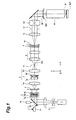
Fig. 1 is a drawing schematically showing a configuration of an exposure apparatus according to an embodiment of the present invention. -
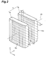
Fig. 2 is a perspective view schematically showing a configuration of a cylindrical micro fly's eye lens. -
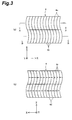
Fig. 3 is a drawing schematically showing a configuration of a micro fly's eye lens for dipole illumination according to the embodiment, wherein (a) is a view from the light source side and (b) a view from the mask side. -
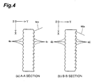
Fig. 4 includes (a) a sectional view along line A-A inFig. 3 (a) and (b) a sectional view along line B-B inFig. 3 (a) . -
Fig. 5 is a drawing schematically showing a secondary light source of a dipole shape formed on the back of the cylindrical micro fly's eye lens in the embodiment. -
Fig. 6 is a drawing to illustrate a configuration and action of a micro fly's eye lens for dipole illumination in a first modification example. -
Fig. 7 is a drawing to illustrate a configuration and action of a micro fly's eye lens for dipole illumination in a second modification example. -
Fig. 8 is a drawing to illustrate a configuration and action of a micro fly's eye lens for dipole illumination in a third modification example. -
Fig. 9 is a view from the light source side of a micro fly's eye lens for quadrupole illumination in a fourth modification example. -
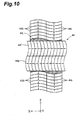
Fig. 10 is a view from the mask side of the micro fly's eye lens for quadrupole illumination in the fourth modification example. -
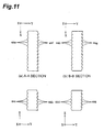
Fig. 11 is sectional views of the micro fly's eye lens for quadrupole illumination in the fourth modification example. -
Fig. 12 is a drawing schematically showing a secondary light source of a cross-shaped quadrupole shape formed with the micro fly's eye lens for quadrupole illumination in the fourth modification example. -
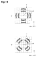
Fig. 13 is a drawing schematically showing a secondary light source of a cross-shaped double quadrupole shape and a secondary light source of an X-shaped double quadrupole shape. -
Fig. 14 is a drawing schematically showing a configuration of a micro fly's eye lens for tripole illumination in a fifth modification example, wherein (a) is a view from the light source side and (b) a view from the mask side. -
Fig. 15 is a drawing schematically showing a secondary light source of a tripole shape formed with the micro fly's eye lens for tripole illumination in the fifth modification example and a configuration of an aperture stop for defining a center pole. -
Fig. 16 is a drawing schematically showing a configuration of a micro fly's eye lens for pentapole illumination in a sixth modification example, wherein (a) is a view from the light source side and (b) a view from the mask side. -
Fig. 17 is a drawing schematically showing a secondary light source of a pentapole shape formed with the micro fly's eye lens for pentapole illumination in the sixth modification example. -
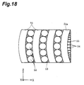
Fig. 18 is a drawing to illustrate another technique for forming a circular surface illuminant of a center pole in the tripole illumination or the pentapole illumination. -
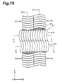
Fig. 19 is a view from the light source side of a micro fly's eye lens for quadrupole illumination with a circumferential polarization state in a seventh modification example. -
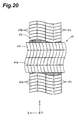
Fig. 20 is a view from the mask side of the micro fly's eye lens for quadrupole illumination with the circumferential polarization state in the seventh modification example. -
Fig. 21 is a sectional view of the micro fly's eye lens for quadrupole illumination with the circumferential polarization state in the seventh modification example. -
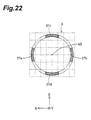
Fig. 22 is a drawing schematically showing a secondary light source of a cross-shaped quadrupole shape formed with the micro fly's eye lens for quadrupole illumination with the circumferential polarization state in the seventh modification example. -
Fig. 23 is a flowchart to illustrate an embodiment of a method for manufacturing the micro fly's eye lens for modified illumination according to each of the embodiment and the modification examples. -
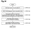
Fig. 24 is a flowchart of a method for obtaining semiconductor devices as micro devices. -
Fig. 25 is a flowchart of a method for obtaining a liquid-crystal display device as a micro device. -
- 1
- light source
- 3
- polarization state switch
- 4, 41-47
- micro fly's eye lens
- 5
- afocal lens
- 7
- conical axicon system
- 8
- zoom lens
- 9
- cylindrical micro fly's eye lens
- 10
- aperture stop
- 11
- condenser optical system
- 12
- mask blind
- 13
- imaging optical system
- M
- mask
- Pl
- projection optical system
- W
- wafer
- Embodiments of the present invention will be described on the basis of the accompanying drawings.
Fig. 1 is a drawing schematically showing a configuration of an exposure apparatus according to an embodiment of the present invention. InFig. 1 , the Z-axis is set along a direction of a normal to a wafer W being a photosensitive substrate, the Y-axis along a direction parallel to the plane ofFig. 1 in a surface of the wafer W, and the X-axis along a direction normal to the plane ofFig. 1 in the surface of the wafer W. With reference toFig. 1 , the exposure apparatus of the present embodiment has alight source 1 for supplying exposure light (illumination light). - The
light source 1 can be, for example, an ArF excimer laser light source for supplying light at the wavelength of 193 nm, a KrF excimer laser light source for supplying light at the wavelength of 248 nm, or the like. Light emitted from thelight source 1 is expanded into a beam of a required sectional shape by a shapingoptical system 2, travels via an automaticaxis tracking unit 2a-2c, thereafter travels through apolarization state switch 3 and a micro fly'seye lens 4 for multi-pole illumination (dipole illumination, quadrupole illumination, or the like), and is then incident to anafocal lens 5. A detailed configuration and action of the micro fly'seye lens 4 for multi-pole illumination will be described later. - The automatic axis tracking unit is composed of at least one
path folding mirror 2a having two or more rotation axes, anangular deviation detector 2b for detecting an angular deviation from the optical axis of the light from thelight source 1, and adriver 2c for rotating (or inclining) thepath folding mirror 2a so as to correct the angular deviation, based on an output from theangular deviation detector 2b, and has a function to keep the angular deviation of light incident to the micro fly'seye lens 4 described below, within a predetermined permissible range. - The
polarization state switch 3 is provided with the following components arranged in the order named from the light source side: aquarter wave plate 3a a crystal optic axis of which is arranged as rotatable around the optical axis AX and which converts elliptically polarized light incident thereinto, into linearly polarized light; ahalf wave plate 3b a crystal optic axis of which is arranged as rotatable around the optical axis AX and which changes a direction of polarization of the linearly polarized light incident thereinto; a depolarizer (depolarizing element) 3c which can be set in or off an illumination optical path. Thepolarization state switch 3, in a state in which thedepolarizer 3c is set off the illumination optical path, has a function to convert the light from thelight source 1 into linearly polarized light with a desired polarization direction and let the linearly polarized light into the micro fly'seye lens 4, and, in a state in which thedepolarizer 3c is set in the illumination optical path, has a function to convert the light from thelight source 1 into substantially unpolarized light and let the unpolarized light into the micro fly'seye lens 4. - The
afocal lens 5 is an afocal system (afocal optic) so set that a front focal position of afront lens unit 5a thereof is approximately coincident with a position of the micro fly'seye lens 4 and that a rear focal position of arear lens unit 5b thereof is approximately coincident with a position of a predetermined plane 6 indicated by a dashed line in the drawing. The micro fly'seye lens 4 for multi-pole illumination, as described later, functions as an optical integrator of a wavefront division type and, when a parallel beam of a rectangular cross section is incident thereinto, it functions to form a light intensity distribution of a multi-pole shape (dipole shape, quadrupole shape, or the like) on the pupil plane of theafocal lens 5. - Therefore, a nearly parallel beam incident into the micro fly's
eye lens 4 forms a light intensity distribution of a multi-pole shape on the pupil plane of theafocal lens 5 and is then emitted in an angular distribution of the multi-pole shape from theafocal lens 5. Aconical axicon system 7 is disposed on or near the pupil plane in the optical path between thefront lens unit 5a and therear lens unit 5b of theafocal lens 5. A configuration and action of theconical axicon system 7 will be described later. - The beam passing through the
afocal lens 5 travels through a zoom lens 8 for variation in σ-value (σ value = mask-side numerical aperture of illumination optical apparatus/mask-side numerical aperture of projection optical system) to enter a cylindrical micro fly'seye lens 9. The cylindrical micro fly'seye lens 9, as shown inFig. 2 , is composed of a first fly'seye member 9a disposed on the light source side, and a second fly'seye member 9b disposed on the mask side. Cylindrical lens groups 9aa and 9ba arrayed in the X-direction are formed each at a pitch p1 in a light-source-side surface of the first fly'seye member 9a and in a light-source-side surface of the second fly'seye member 9b, respectively. - On the other hand, cylindrical lens groups 9ab and 9bb arrayed in the Z-direction are formed each at a pitch p2 (p2 > p1) in a mask-side surface of the first fly's
eye member 9a and in a mask-side surface of the second fly'seye member 9b, respectively. When attention is focused on refraction in the X-direction (or refraction in the XY plane) of the cylindrical micro fly'seye lens 9, a parallel beam incident along the optical axis AX is wavefront-divided at the pitch p1 along the X-direction by the cylindrical lens group 9aa formed on the light source side of the first fly'seye member 9a and is condensed by its refracting surface, and thereafter divided wavefront sections are condensed by refracting surfaces of the corresponding cylindrical lenses in the cylindrical lens group 9ba formed on the light source side of the second fly'seye member 9b, to be converged on the rear focal plane of the cylindrical micro fly'seye lens 9. - On the other hand, when attention is focused on refraction in the Z-direction (or refraction in the YZ plane) of the cylindrical micro fly's
eye lens 9, the parallel beam incident along the optical axis AX is wavefront-divided at the pitch p2 along the Z-direction by the cylindrical lens group 9ab formed on the mask side of the first fly'seye member 9a and condensed by its refracting surface, and thereafter divided wavefront sections are condensed by refracting surfaces of the corresponding cylindrical lenses in the cylindrical lens group 9bb formed on the mask side of the second fly'seye member 9b, to be converged on the rear focal plane of the cylindrical micro fly'seye lens 9. - As described above, the cylindrical micro fly's
eye lens 9 is composed of the first fly'seye member 9a and the second fly'seye member 9b each of which has the cylindrical lens groups disposed on both side faces, and exhibits an optical function similar to that of a micro fly's eye lens in which a large number of rectangular microscopic refracting surfaces having the size of p1 in the X-direction and the size of p2 in the Z-direction are integrally formed vertically and horizontally and densely. With the cylindrical micro fly'seye lens 9, it is feasible to hold down change in distortion due to variation in surface shape of microscopic refracting surfaces, e.g., to keep down influence of a manufacturing error of the large number of microscopic refracting surfaces integrally formed by etching, on the illuminance distribution. - The position of the predetermined plane 6 is located near the front focal position of the zoom lens 8 and the entrance surface of the cylindrical micro fly's
eye lens 9 is located near the rear focal position of the zoom lens 8. In other words, the zoom lens 8 keeps the predetermined plane 6 and the entrance surface of the cylindrical micro fly'seye lens 9 substantially in the Fourier transform relation and, therefore, keeps the pupil plane of theafocal lens 5 optically substantially conjugate with the entrance surface of the cylindrical micro fly'seye lens 9. - Accordingly, for example, an illumination field of a multi-pole shape centered on the optical axis AX is formed on the entrance surface of the cylindrical micro fly's
eye lens 9 as on the pupil plane of theafocal lens 5. The overall shape of this illumination field of a multi-pole shape similarly varies depending upon the focal length of the zoom lens 8. The rectangular microscopic refracting surfaces as wavefront division units in the cylindrical micro fly'seye lens 9 are similar to a shape of an illumination field to be formed on the mask M (or a shape of an exposure region to be formed on the wafer W eventually). - A beam incident into the cylindrical micro fly's
eye lens 9 is two-dimensionally divided and a secondary light source having a light intensity distribution substantially identical with the illumination field formed by the incident beam, i.e., a secondary light source consisting of substantial surface illuminants of the multi-pole shape centered on the optical axis AX is formed on or near the rear focal plane of the cylindrical micro fly's eye lens 9 (therefore, on an illumination pupil). Beams from the secondary light source formed on or near the rear focal plane of the cylindrical micro fly'seye lens 9 are then incident to anaperture stop 10 disposed near it. - The
aperture stop 10 has an aperture (light transmitting portion) of a multi-pole shape corresponding to the secondary light source of the multi-pole shape formed on or near the rear focal plane of the cylindrical micro fly'seye lens 9. Theaperture stop 10 is so arranged that it can be set in or off the illumination optical path and that it can be switched to one of other aperture stops with an aperture different in size and shape. The aperture stops can be switched, for example, by such a method as a well-known turret method or slide method. Theaperture stop 10 is located at a position optically substantially conjugate with an entrance pupil plane of a projection optical system PL described below, to defme a range of contribution of the secondary light source to illumination. - Light beams from the secondary light source limited by the
aperture stop 10 travel through a condenseroptical system 11 to illuminate a mask blind 12 in a superimposed manner. In this manner, a rectangular illumination field according to the shape and focal length of the rectangular microscopic refracting surfaces as wavefront division units in the cylindrical micro fly'seye lens 9 is formed on themask blind 12 as an illumination field stop. The beams passing through a rectangular aperture (light transmitting portion) of themask blind 12 are condensed by an imagingoptical system 13 to illuminate the mask M with a predetermined pattern therein in a superimposed manner. Namely, the imagingoptical system 13 forms an image of the rectangular aperture of themask blind 12 on the mask M. - A beam transmitted by the pattern of the mask M held on a mask stage MS travels through the projection optical system PL to form an image of the mask pattern on the wafer (photosensitive substrate) W held on a wafer stage WS. In this configuration, the pattern of the mask M is sequentially transferred into each of exposure areas on the wafer W by carrying out one-shot exposure or scan exposure while two-dimensionally driving and controlling the wafer stage WS and, therefore, two-dimensionally driving and controlling the wafer W in the plane (XY plane) perpendicular to the optical axis AX of the projection optical system PL.
- Modified illuminations of various forms can be implemented, for example, by setting a micro fly's eye lens with an appropriate property like a micro fly's eye lens for annular illumination or a micro fly's eye lens for circular illumination in the illumination optical path, instead of the micro fly's
eye lens 4 for multi-pole illumination. The micro fly's eye lens can be switched to another, for example, by such a method as the well-known turret method or slide method. - The
conical axicon system 7 is composed of afirst prism member 7a with a plane on the light source side and a refracting surface of a concave conical shape on the mask side, and asecond prism member 7b with a plane on the mask side and a refracting surface of a convex conical shape on the light source side, which are arranged in order from the light source side. The refracting surface of the concave conical shape of thefirst prism member 7a and the refracting surface of the convex conical shape of thesecond prism member 7b are complementarily formed so as to abut on each other. At least one of thefirst prism member 7a and thesecond prism member 7b is arranged as movable along the optical axis AX to make the distance variable between the refracting surface of the concave conical shape of thefirst prism member 7a and the refracting surface of the convex conical shape of thesecond prism member 7b. For easier understanding, the action of theconical axicon system 7 and the action of the zoom lens 8 will be described with focus on the secondary light source of an annular shape or quadrupole shape. - In a state in which the concave conical refracting surface of the
first prism member 7a and the convex conical refracting surface of thesecond prism member 7b are in contact with each other, theconical axicon system 7 functions as a plane-parallel plate and has no effect on the annular or quadrupolar secondary light source formed. However, as the concave conical refracting surface of thefirst prism member 7a is separated away from the convex conical refracting surface of thesecond prism member 7b, the outside diameter (inside diameter) of the annular or quadrupolar secondary light source varies while the width of the annular or quadrupolar secondary light source (half of a difference between the outside diameter and the inside diameter of the annular secondary light source; half of a difference between a diameter (outside diameter) of a circle circumscribed to the quadrupolar secondary light source and a diameter (inside diameter) of a circle inscribed in the quadrupolar secondary light source) is kept constant. Namely, the separation results in varying the annular ratio (inside diameter/outside diameter) and the size (outside diameter) of the annular or quadrupolar secondary light source. - The zoom lens 8 has a function to similarly enlarge or reduce the overall shape of the annular or quadrupolar secondary light source. For example, when the focal length of the zoom lens 8 is increased from a minimum to a predetermined value, the overall shape of the annular or quadrupolar secondary light source is similarly enlarged. In other words, the action of the zoom lens 8 is to vary both the width and size (outside diameter), without change in the annular ratio of the annular or quadrupolar secondary light source. In this manner, the annular ratio and size (outside diameter) of the annular or quadrupolar secondary light source can be controlled by the actions of the
conical axicon system 7 and the zoom lens 8. -
Fig. 3 is a drawing schematically showing a configuration of a micro fly's eye lens for dipole illumination according to the present embodiment, wherein (a) is a view from the light source side and (b) a view from the mask side.Fig. 4 (a) is a sectional view along line A-A inFig. 3 (a) andFig. 4 (b) a sectional view along line B-B inFig. 3 (a) . The micro fly'seye lens 4 for dipole illumination in the present embodiment is constructed as a single optical member (optically transparent member) made, for example, of fluorite (CaF2: calcium fluoride). - The following refracting surface regions are formed on the entrance side (light source side) of the micro fly's
eye lens 4, as shown inFig. 3 (a) : a large number of first refractingsurface regions 4a having an arcuate contour with the center projecting in the -X-direction (first direction); and a large number of second refractingsurface regions 4b having an arcuate contour with the center projecting in the +X-direction (second direction). Each of the arcuate contours of the first refractingsurface regions 4a and the second refractingsurface regions 4b corresponds to a contour of a partial region along a circumferential direction of an annular region. - More specifically, the arcuate contour of the first refracting
surface regions 4a and the second refractingsurface regions 4b, as described below with reference toFig. 5 , corresponds to an arcuate contour defined by two parallel line segments (corresponding to 20e, 20f inFig. 5 ) separated by an equal distance from a center of an annular region, an inside circle of the annular region (corresponding to 20d inFig. 5 ), and an outside circle of the annular region (corresponding to 20c inFig. 5 ). It is, however, noted that when the arcuate contour defined by the two line segments and two circles is faithfully applied to the refractingsurface regions surface regions Fig. 3 (a) , because the curvature of the inside arc is slightly different from that of the outside arc. - For easier understanding of the configuration, it is assumed in the present embodiment that the arcuate contour of each refracting
surface region surface regions - Each refracting
surface region surface region surface region Fig. 4 (a) and (b) . - For simpler description, it is also assumed in the present embodiment that the spherical curvature of the first refracting
surface regions 4a is equal to that of the second refractingsurface regions 4b and that the contour of the first refractingsurface regions 4a is equal to the contour of the second refractingsurface regions 4b. Namely, the contour of the first refractingsurface regions 4a and the contour of the second refractingsurface regions 4b are symmetric with respect to the Z-direction (third direction) and, in turn, are opposite to each other along the X-direction. In this case, the first refractingsurface regions 4a and the second refractingsurface regions 4b are continuously formed and no border line extending in the X-direction actually appears between the first refractingsurface regions 4a and the second refractingsurface regions 4b. However, a border line is illustrated between the first refractingsurface regions 4a and the second refractingsurface regions 4b for clarity of the drawing inFig. 3 (a) . In the configuration wherein the first refractingsurface regions 4a and the second refractingsurface regions 4b are continuously formed and wherein there is no level difference between the first refractingsurface regions 4a and the second refractingsurface regions 4b, it is feasible to reduce (or suppress) occurrence of unwanted light that directly passes through the micro fly's eye lens 4 (or that travels straight to be transmitted). - On the other hand, the following deflecting surface regions are formed on the exit side (mask side) of the micro fly's
eye lens 4, as shown inFig. 3 (b) : a large number of first deflectingsurface regions 4c of an arcuate contour densely arranged along the X-direction so as to correspond to the large number of first refractingsurface regions 4a; and a large number of second deflectingsurface regions 4d of an arcuate contour densely arranged along the X-direction so as to correspond to the large number of second refractingsurface regions 4b. Each deflectingsurface region surface region - More specifically, each first
deflecting surface region 4c, as shown inFig. 4 (a) , has a planar shape with an up slope relative to the +X-direction, i.e., a planar shape inclined so as to be projecting toward the mask side with respect to the +X-direction. On the other hand, each seconddeflecting surface region 4d, as shown inFig. 4 (b) , has a planar shape with an up slope relative to the -X-direction, i.e., a planar shape inclined so as to be projecting toward the mask side with respect to the -X-direction. In other words, each firstdeflecting surface region 4c has a planar shape defined by a first normal 4ca inclined relative to the X-direction, and each seconddeflecting surface region 4d has a planar shape defined by a second normal 4da inclined reversely to the first normal 4ca and relative to the X-direction. - In
Fig. 3 (b) , for easier understanding of the configuration, each deflectingsurface region deflecting surface region 4c is provided with an arrow directed in the +X-direction and each seconddeflecting surface region 4d is provided with an arrow directed in the -X-direction. For clarity of the drawing,Fig. 3 shows only some of the large number of refractingsurface regions surface regions eye lens 4. This also applies toFig. 6 (a) ,Fig. 7 (a) ,Fig. 8 (a) ,Fig. 9 ,Fig. 10 ,Fig. 14 ,Fig. 16 , andFig. 18 associated withFig. 3 . - The micro fly's
eye lens 4 is formed, for example, by physically processing a plane-parallel plate made of fluorite (e.g., micromachining, processing with a die in a high temperature state, or the like). At this time, the plane-parallel plate made of fluorite belonging to the cubic system is preferably one with the crystal plane {111} directed to the optical axis AX (i.e., to the traveling direction of the incident light to each refractingsurface region surface 4a), it is also feasible to well suppress the influence of birefringence of fluorite. - In the micro fly's
eye lens 4 for dipole illumination in the present embodiment, the nearly parallel beam of the rectangular shape incident thereto from thelight source 1 is wavefront-divided by the large number of wavefront dividing regions, i.e., the large number of arcuate first refracting surface regions (first wavefront dividing regions) 4a and the large number of arcuate second refracting surface regions (second wavefront dividing regions) 4b. A beam refracted by each first refractingsurface region 4a is guided to each corresponding first deflectingsurface region 4c and a beam refracted by each second refractingsurface region 4b is guided to each corresponding second deflectingsurface region 4d. - Beams guided through the respective first refracting
surface regions 4a to the respective corresponding first deflectingsurface regions 4c and beams guided through the respective second refractingsurface regions 4b to the respective corresponding second deflectingsurface regions 4d form a light intensity distribution of a dipole shape arranged in the X-direction and in symmetry with respect to the optical axis AX on the pupil plane of theafocal lens 5, in a superimposed manner. In this way, an illumination field of a dipole shape arranged in the X-direction and in symmetry with respect to the optical axis AX is formed on the entrance surface of the cylindrical micro fly'seye lens 9 as on the pupil plane of theafocal lens 5, as described above. Furthermore, a secondary light source of a dipole shape consisting of a pair ofsubstantial surface illuminants Fig. 5 , is formed on or near the rear focal plane of the cylindrical micro fly'seye lens 9. - The pair of
surface illuminants outside circle 20c of an annular region centered on the optical axis AX, aninside circle 20d of the annular region, and twoparallel line segments surface region surface illuminants circles line segments - In this manner, the beams guided through the respective first refracting
surface regions 4a to the respective corresponding first deflectingsurface regions 4c are deflected by the first deflectingsurface regions 4c with the planar shape of the up slope relative to the +X-direction to illuminate a light intensity distribution corresponding to onearcuate surface illuminant 20a among the secondary light source of the dipole shape, in a superimposed manner. The beams guided through the respective second refractingsurface regions 4b to the respective corresponding second deflectingsurface regions 4d are deflected by the seconddeflecting surface regions 4d with the planar shape of the up slope relative to the -X-direction to form a light intensity distribution corresponding to the otherarcuate surface illuminant 20b among the secondary light source of the dipole shape, in a superimposed manner. For making the light intensity on thesurface illuminant 20a substantially coincident with the light intensity on thesurface illuminant 20b, the number of first refractingsurface regions 4a is preferably approximately equal to the number of second refractingsurface regions 4b. - In
Fig. 5 , for clarity of the drawing, the rectangular microscopic refracting surfaces as wavefront division units in the cylindrical micro fly'seye lens 9 are indicated by dashed lines and the number of refracting surfaces depicted is much smaller than the actual number. This also applies toFig. 6 (b) ,Fig. 7 (b) ,Fig. 8 (b) ,Fig. 12 ,Fig. 13 ,Fig. 15 (a) , andFig. 17 associated withFig. 5 . - As described above, the micro fly's
eye lens 4 for dipole illumination in the present embodiment is provided with the large number of arcuate first refractingsurface regions 4a and second refractingsurface regions 4b as wavefront dividing regions. It also has the large number of arcuate first deflectingsurface regions 4c corresponding to the large number of first refractingsurface regions 4a and the large number of arcuate second deflectingsurface regions 4d corresponding to the large number of arcuate second refractingsurface regions 4b. The arcuate contour of the first refractingsurface regions 4a and the arcuate contour of the second refractingsurface regions 4b are symmetric with respect to the Z-direction (or opposite to each other along the X-direction), and the first refractingsurface regions 4a and second deflectingsurface regions 4d have beam deflecting actions opposite to each other along the X-direction. - Accordingly, the beams guided through the respective first refracting
surface regions 4a to the respective corresponding first deflectingsurface regions 4c and the beams guided through the respective second refractingsurface regions 4b to the respective corresponding second deflectingsurface regions 4d are deflected by the first deflectingsurface regions 4c and by the seconddeflecting surface regions 4d, respectively, to form the secondary light source of the dipole shape consisting of the pair ofarcuate surface illuminants eye lens 9. Thefirst surface illuminant 20a is formed in an arcuate first region being a portion along the circumferential direction of the annular region centered on the optical axis AX and thesecond surface illuminant 20b is formed in an arcuate second region being a portion along the circumferential direction of the annular region and being symmetric with the first region with respect to the optical axis AX. - Namely, the pair of
arcuate surface illuminants eye lens 4 for dipole illumination in the present embodiment has the function to form the far field pattern of the dipole shape having the first region of a portion along the circumferential direction of the annular region and the second region of another portion along the circumferential direction of the annular region, based on the incident light. - As a result, the present embodiment is able to hold down the light-quantity loss at the
aperture stop 10, while only a small amount of beams from the secondary light source of the dipole shape (20a, 20b) is blocked by the aperture of the dipole shape of theaperture stop 10. Since in the present embodiment the dipole light intensity distribution of any desired shape is formed by the micro fly'seye lens 4 having the very small wavefront dividing surfaces and the cylindrical micro fly'seye lens 9 having the very small unit wavefront dividing surfaces, the secondary light source of the dipole shape (20a, 20b) does not always have to be limited by theaperture stop 10, according to circumstances. - Since in the present embodiment the pair of
arcuate surface illuminants - For forming the pattern image with high contrast, the annular ratio of the dipole secondary light source (20a, 20b) (or the diameter of the
inside circle 20d/the diameter of theoutside circle 20c inFig. 5 ) is preferably set, for example, to 8/10 or more. For forming the pattern image with high contrast and ensuring a sufficient superposition tolerance of beams onto thearcuate surface illuminants arcuate surface illuminants line segments arcuate surface illuminant 20a inFig. 5 ) θ is preferably, for example, in the range of approximately 35° to 40°. - In passing, a conventional fly's eye lens having only the wavefront division function forms a secondary light source of a rectangular shape (or a regular hexagonal shape or the like) similar to the shape of the wavefront dividing surfaces of the fly's eye lens. For this reason, for forming the pattern image with high contrast in the conventional technology, it is necessary to limit a beam from the secondary light source of the rectangular shape by an aperture of a dipole shape with a large annular ratio, which results in occurrence of a large light-quantity loss at the aperture stop.
- Since in the present embodiment the micro fly's
eye lens 4 for dipole illumination is constructed as a single optical member (optically transparent member) made of fluorite, or since the plurality of refractingsurface regions surface regions - In this manner, the illumination optical apparatus (1-13) of the present embodiment is able to keep down the light-quantity loss at the
aperture stop 10 in the modified illumination such as the dipole illumination and to stably illuminate the mask (illumination target surface) M under a desired illumination condition, using the micro fly's eye lens (optical integrator) 4 with the sufficient durability to light in the ultraviolet region of short wavelengths. The exposure apparatus (1-PL) of the present embodiment is able to stably perform good exposure under a desired illumination condition, using the illumination optical apparatus for stably illuminating the mask M under a desired illumination condition. - In the above-described embodiment, the large number of first refracting
surface regions 4a of the arcuate shape with the center projecting in the -X-direction and the large number of second refractingsurface regions 4b of the arcuate shape with the center projecting in the +X-direction are densely arranged along the X-direction. Namely, the projecting direction of the center of the first refractingsurface regions 4a and the projecting direction of the center of the second refractingsurface regions 4b are set opposite to each other along one straight line. However, without having to be limited to this, it is also possible to adopt a configuration example in which the projecting direction of the center of the first refracting surface regions and the projecting direction of the center of the second refracting surface regions are not set opposite to each other along one straight line. In this case, however, the pair of arcuate surface illuminants constituting the secondary light source of the dipole shape are not formed at positions symmetric with respect to the optical axis. - In the above-described embodiment, each of the first refracting
surface regions 4a and the second refractingsurface regions 4b has the parallel type arcuate contour defined approximately by the two parallel line segments separated by the same distance from the center of the annular region, the inside circle of the annular region, and the outside circle of the annular region. However, without having to be limited to this, the same effect as in the above embodiment is also obtained in a modification example in which a nonparallel type arcuate contour defined approximately by two line segments extending radially at a predetermined angle from the center of the annular region, the inside circle of the annular region, and the outside circle of the annular region is applied to the first refracting surface regions and the second refracting surface regions. -
Fig. 6 is a drawing to illustrate a modification example in which the nonparallel type arcuate contour is applied to the first refracting surface regions and the second refracting surface regions. With reference toFig. 6 (a) , a micro fly'seye lens 41 for dipole illumination in the first modification example has a large number of first refractingsurface regions 41a having a nonparallel type arcuate contour with the center projecting in the -X-direction, and a large number of second refractingsurface regions 41b having a nonparallel type arcuate contour with the center projecting in the +X-direction. The micro fly'seye lens 41 also has a large number of nonparallel type arcuate first deflecting surface regions 41 c corresponding to the large number of first refractingsurface regions 41 a, and a large number of nonparallel type arcuate second deflecting surface regions 41 d corresponding to the large number of arcuate second refractingsurface regions 41b though they are not illustrated in the drawing. - In this manner, the secondary light source of the dipole shape consisting of a pair of nonparallel type
arcuate surface illuminants Fig. 6 (b) , by action of the micro fly'seye lens 41 in the first modification example. Each of the pair ofsurface illuminants outside circle 21 c of an annular region centered on the optical axis AX, aninside circle 21 d of the annular region, and twoline segments surface regions 41a and the second refractingsurface regions 4 1 b along the X-direction, it is also preferable to apply a contour resulting from slight modification of the faithful arcuate shape obtained from the annular region, to the first refractingsurface regions 41 a and the second refractingsurface regions 41 b. - Namely, it is preferable to apply to the first refracting
surface regions 41 a and the second refractingsurface regions 41b, an arcuate contour obtained by making the curvature of the inside arc coincident with that of the outside arc or by making the curvature of the outside arc coincident with that of the inside arc, from the arcuate shape defined by the two line segments extending radially from the center of the annular region (corresponding to 21e, 21f inFig. 6 (b) ), the inside circle of the annular region (corresponding to 21d inFig. 6 (b) ), and the outside circle of the annular region (corresponding to 21c inFig. 6 (b) ). - In the above-described embodiment, each of the first refracting
surface regions 4a and the second refractingsurface regions 4b has the arcuate contour corresponding to a partial region along the circumferential direction of the annular region. However, without having to be limited to this, it is also possible to apply to at least either of the first refracting surface regions and the second refracting surface regions, generally, an arcuate contour with the center projecting in a predetermined direction, e.g., a contour curved in an arcuate shape or a contour bent in an arcuate shape. Specifically, the same effect as in the aforementioned embodiment is also achieved by applying a contour bent in a chevron shape as shown inFig. 7 or a contour bent in a compressed chevron shape as shown inFig. 8 , to the first refracting surface regions and the second refracting surface regions. - With reference to
Fig. 7 (a) , a micro fly'seye lens 42 for dipole illumination in the second modification example is arranged so that each of first refractingsurface regions 42a and second refractingsurface regions 42b has a contour of a hexagonal shape bent in a chevron shape. Accordingly, a secondary light source of a dipole shape consisting of a pair ofsurface illuminants Fig. 7 (b) , by action of the micro fly'seye lens 42 in the second modification example. - With reference to
Fig. 8 (a) , a micro fly'seye lens 43 for dipole illumination in the third modification example is arranged so that each of first refractingsurface regions 43a and second refractingsurface regions 43b has a contour of an octagonal shape bent in a compressed chevron shape. Accordingly, a secondary light source of a dipole shape consisting of a pair ofsurface illuminants Fig. 8 (b) , by action of the micro fly'seye lens 43 in the third modification example. - As described above, a variety of modification examples can be contemplated as to the contours, the number, the arrangement, etc. of the first refracting surface regions and the second refracting surface regions in the micro fly's
eye lens 4 for dipole illumination in the embodiment shown inFigs. 3 to 5 . - The above description shows the examples of the dipole illumination, but, without having to be limited to it, a micro fly's eye lens for quadrupole illumination can also be implemented based on a configuration similar to that in the embodiment in
Figs. 3 to 5 . A micro fly's eye lens for quadrupole illumination in the fourth modification example will be described below with reference toFigs. 9 to 12 . With reference toFig. 9 , the following refracting surface regions are formed on the entrance side (light source side) of the micro fly'seye lens 44 for quadrupole illumination in the fourth modification example: a large number of first refractingsurface regions 44a of an arcuate shape with the center projecting in the -X-direction; a large number of second refractingsurface regions 44b of an arcuate shape with the center projecting in the +X-direction; a large number of third refractingsurface regions 44c of an arcuate shape with the center projecting in the +Z-direction; and a large number of fourth refractingsurface regions 44d of an arcuate shape with the center projecting in the -Z-direction. - The first refracting
surface regions 44a and the second refractingsurface regions 44b have respective configurations corresponding to the first refractingsurface regions 4a and the second refractingsurface regions 4b in the micro fly'seye lens 4 for dipole illumination shown inFigs. 3 to 5 . The third refractingsurface regions 44c have a configuration obtained by rotating the first refractingsurface regions 44a by 90° clockwise in the drawing, and the fourth refractingsurface regions 44d have a configuration obtained by rotating the second refractingsurface regions 44b by 90° clockwise in the drawing.Regions 44e hatched in the drawing are shield regions between the first and second refractingsurface regions surface regions - On the other hand, the following deflecting surface regions are formed on the exit side (mask side) of the micro fly's
eye lens 44 for quadrupole illumination, as shown inFig. 10 : a large number of arcuate first deflectingsurface regions 44f densely arranged along the X-direction corresponding to the large number of first refractingsurface regions 44a; a large number of arcuate second deflectingsurface regions 44g densely arranged along the X-direction corresponding to the large number of second refractingsurface regions 44b; a large number of arcuate third deflectingsurface regions 44h densely arranged along the Z-direction corresponding to the large number of third refractingsurface regions 44c; a large number of arcuate fourth deflectingsurface regions 44i densely arranged along the Z-direction corresponding to the large number of fourth refractingsurface regions 44d.Regions 44j hatched in the drawing are shield regions between the first and second deflectingsurface regions surface regions side shield regions 44j are provided corresponding to the entrance-side shield regions 44e. - With reference to
Figs. 10 and11 , the first deflectingsurface regions 44f have a planar shape with an up slope relative to the +X-direction as the first deflectingsurface regions 4c in the micro fly'seye lens 4 for dipole illumination, and the seconddeflecting surface regions 44g have a planar shape with an up slope relative to the -X-direction as the seconddeflecting surface regions 4d. The thirddeflecting surface regions 44h have a configuration obtained by rotating the first deflectingsurface regions 44f by 90° counterclockwise in the drawing, and the fourth deflectingsurface regions 44i have a configuration obtained by rotating the seconddeflecting surface regions 44g by 90° counterclockwise in the drawing. Namely, the thirddeflecting surface regions 44h have a planar shape with an up slope relative to the -Z-direction and the fourth deflectingsurface regions 44i have a planar shape with an up slope relative to the +Z-direction. - In this manner, the secondary light source is formed in a cross-shaped quadrupole shape consisting of a pair of
arcuate surface illuminants arcuate surface illuminants Fig. 12 , by action of the micro fly'seye lens 44 in the fourth modification example. For approximately matching light intensities on therespective surface illuminants 24a-24d with each other, it is preferable to make the number of first refractingsurface regions 44a, the number of second refractingsurface regions 44b, the number of third refractingsurface regions 44c, and the number of fourth refractingsurface regions 44d approximately equal to each other. - In the fourth modification example, for example, a mask pattern with the pitch direction along a direction optically corresponding to the X-direction on the illumination pupil and a mask pattern with the pitch direction along a direction optically corresponding to the Z-direction on the illumination pupil can be illuminated with beams of a high NA corresponding to the maximum numerical aperture (NA) of the illumination optical apparatus (1-13), so that pattern images can be formed with high contrast on the wafer W.
- It is also possible to apply other appropriate arcuate contours as shown in the first modification example to the third modification example, to the micro fly's
eye lens 44 for quadrupole illumination in the fourth modification example. Namely, various modification examples can be contemplated as to the contours, numbers, arrangement, etc. of the respective refracting surface regions in the fourth modification example and various modification examples can also be contemplated as to the surface shape of each deflecting surface region and others. - Specifically, in the fourth modification example each deflecting
surface region 44f-44i has a planar shape defined by a normal of one kind. Namely, the large number of first deflectingsurface regions 44f have their respective planar shapes parallel to each other; the large number of second deflectingsurface regions 44g have their respective planar shapes parallel to each other; the large number of third deflectingsurface regions 44h have their respective planar shapes parallel to each other; the large number of fourth deflectingsurface regions 44i have their respective planar shapes parallel to each other. However, without having to be limited to this, a secondary light source of a cross-shaped double quadrupole shape as shown inFig. 13 (a) , i.e., a secondary light source of an octupole shape can be formed, for example, based on a configuration in which each deflecting surface region has a shape of planes defined by normals of two kinds. - For forming a secondary light source of an X-shaped double quadrupole shape as shown in
Fig. 13 (b) , it is necessary to define a shape of planes of each deflecting surface region by normals of two kinds and to rotate the arrangement of the large number of refracting surface regions and deflecting surface regions by 45° around the Y-axis, in the micro fly'seye lens 44 for quadrupole illumination in the fourth modification example. In the embodiment ofFigs. 3 to 5 and the first modification example to the third modification example, the planar shape of each deflecting surface region can be defined by normals of two kinds, when necessary, to form a secondary light source of a double dipole shape (not shown). - Furthermore, a micro fly's eye lens for tripole illumination can be realized based on a configuration similar to that in the embodiment of
Figs. 3 to 5 . The micro fly's eye lens for tripole illumination according to the fifth modification example will be described below with reference toFigs. 14 and15 . With reference toFig. 14 (a) , the following refracting surface regions are formed on the entrance side (light source side) of the micro fly'seye lens 45 for tripole illumination according to the fifth modification example: a large number of first refractingsurface regions 45a of an arcuate shape with the center projecting in the -X-direction; a large number of second refractingsurface regions 45b of an arcuate shape with the center projecting in the +X-direction. A large number of third refractingsurface regions 45c are formed between two adjacent first refractingsurface regions 45a and between two adjacent second refractingsurface regions 45b. - The first refracting
surface regions 45a and the second refractingsurface regions 45b have respective configurations corresponding to those of the first refractingsurface regions 4a and the second refractingsurface regions 4b in the micro fly'seye lens 4 for dipole illumination shown inFigs. 3 to 5 . On the other hand, the third refractingsurface regions 45c have a contour of a nearly rectangular shape (or an arcuate shape close to a square) obtained by dividing each arcuate region corresponding to the first refractingsurface regions 45a and the second refractingsurface regions 45b in the Z-direction (Fig. 14 shows an example of division into five equal parts). The third refractingsurface regions 45c have a convex shape (or concave shape) as the first refractingsurface regions 45a and the second refractingsurface regions 45b, and have a function to refract incident light. - In general, it is possible to apply various surface shapes, for example, including a part of a spherical surface, a part of a rotationally symmetric aspherical surface, and a part of a rotationally asymmetric aspherical surface (e.g., a toric surface) to the surface shape of each third refracting
surface region 45c, as in the case of the first refractingsurface regions 45a and the second refractingsurface regions 45b. For simpler description, it is assumed in the fifth modification example that each third refractingsurface region 45c has a spherical convex shape symmetric with respect to each center axis parallel to the optical axis AX, for example. - On the other hand, the following deflecting surface regions are formed on the exit side (mask side) of the micro fly's
eye lens 45 for tripole illumination, as shown inFig. 14 (b) : a large number of arcuate first deflectingsurface regions 45d arranged along the X-direction corresponding to the large number of first refractingsurface regions 45a; a large number of arcuate second deflectingsurface regions 45e arranged along the X-direction corresponding to the large number of second refractingsurface regions 45b; a large number of nearly rectangular third deflectingsurface regions 45f arranged corresponding to the large number of third refractingsurface regions 45c. - The first
deflecting surface regions 45d have a planar shape with an up slope relative to the +X-direction as the first deflectingsurface regions 4c in the micro fly'seye lens 4 for dipole illumination, and the seconddeflecting surface regions 45e have a planar shape with an up slope relative to the -X-direction as the seconddeflecting surface regions 4d. On the other hand, the thirddeflecting surface regions 45f have a planar shape perpendicular to the optical axis AX (and, therefore, perpendicular to the Y-axis) and have a function to transmit rays incident through the corresponding third refractingsurface regions 45c and in parallel with the optical axis AX, without change in their traveling direction. - Accordingly, nearly parallel beams guided through the respective third refracting
surface regions 45c to the respective corresponding third deflectingsurface regions 45f are not substantially subjected to deflection in the respective third deflectingsurface regions 45f, to form a light intensity distribution of a nearly circular shape centered on the optical axis AX on the illumination pupil plane, in a superimposed manner. In this way, a secondary light source of a tripole shape is formed as one consisting of a pair ofarcuate surface illuminants surface illuminant 25c of a nearly circular shape centered on the optical axis AX, as shown inFig. 15 (a) , by action of the micro fly'seye lens 45 in the fifth modification example. - For obtaining an accurate light intensity distribution of a circular shape centered on the optical axis AX on the illumination pupil plane, it is preferable to limit light reaching the
surface illuminant 25c of the center pole or light from thesurface illuminant 25c, by a circular aperture (light transmitting portion) of an aperture member 10aa for the center pole in anaperture stop 10a shown inFig. 15 (b) . Theaperture stop 10a is provided with an outside aperture member 10ab having a circular aperture defined by a circle circumscribed to the pair ofarcuate surface illuminants - Similarly, a micro fly's eye lens for pentapole illumination can be realized based on a configuration similar to that in the fourth modification example of
Figs. 9 to 12 . The micro fly's eye lens for pentapole illumination according to the sixth modification example will be described below with reference toFigs. 16 and17 . With reference toFig. 16 (a) , the following refracting surface regions are formed on the entrance side (light source side) of the micro fly'seye lens 46 for pentapole illumination in the sixth modification example: a large number of first refractingsurface regions 46a of an arcuate shape with the center projecting in the -X-direction; a large number of second refractingsurface regions 46b of an arcuate shape with the center projecting in the +X-direction; a large number of third refractingsurface regions 46c of an arcuate shape with the center projecting in the +Z-direction; a large number of fourth refractingsurface regions 46d of an arcuate shape with the center projecting in the -Z-direction. Furthermore, a large number of fifth refractingsurface regions 46e are formed between two adjacent first refractingsurface regions 46a, between two adjacent second refractingsurface regions 46b, between two adjacent third refractingsurface regions 46c, and between two adjacent fourth refractingsurface regions 46d. - The first refracting
surface regions 46a to the fourth refractingsurface regions 46d have respective configurations corresponding to the first refractingsurface regions 44a to the fourth refractingsurface regions 44d in the micro fly'seye lens 44 for quadrupole illumination shown inFigs. 9 to 12 . On the other hand, the fifth refractingsurface regions 46e have a contour of a nearly rectangular shape (or an arcuate shape close to a square) obtained by dividing an arcuate region corresponding to the first refractingsurface regions 46a and the second refractingsurface regions 46b in the Z-direction (Fig. 16 shows an example of division into five equal parts), or a contour of a nearly rectangular shape (or an arcuate shape close to a square) obtained by dividing an arcuate region corresponding to the third refractingsurface regions 46c and the fourth refractingsurface regions 46d in the X-direction (Fig. 16 shows an example of division into five equal parts). - Namely, the fifth refracting
surface regions 46e formed between two adjacent first refractingsurface regions 46a and between two adjacent second refractingsurface regions 46b have a configuration corresponding to that of the third refractingsurface regions 45c in the fifth modification example. The fifth refractingsurface regions 46e formed between two adjacent third refractingsurface regions 46c and between two adjacent fourth refractingsurface regions 46d have a configuration obtained by rotating the third refractingsurface regions 45c in the fifth modification example by 90° in the drawing. The fifth refractingsurface regions 46e have a convex shape (or concave shape) as the third refractingsurface regions 45c in the fifth modification example, and have a function to refract incident light.Shield regions 46f are provided between the first and second refractingsurface regions surface regions - On the other hand, the following regions are formed on the exit side (mask side) of the micro fly's
eye lens 46 for pentapole illumination, as shown inFig. 16 (b) : a large number of arcuate first deflectingsurface regions 46g arranged along the X-direction corresponding to the large number of first refractingsurface regions 46a; a large number of arcuate second deflectingsurface regions 46h arranged along the X-direction corresponding to the large number of second refractingsurface regions 46b; a large number of arcuate third deflectingsurface regions 46i arranged along the Z-direction corresponding to the large number of third refractingsurface regions 46c; a large number of arcuate fourth deflectingsurface regions 46j arranged along the Z-direction corresponding to the large number of fourth refractingsurface regions 46d; a large number of nearly rectangular fifth deflectingsurface regions 46k arranged corresponding to the large number of fifth refractingsurface regions 46e; shieldregions 46m arranged corresponding to theshield regions 46f. - The first
deflecting surface regions 46g have a planar shape with an up slope relative to the +X-direction as the first deflectingsurface regions 44f in the micro fly'seye lens 44 for quadrupole illumination; the seconddeflecting surface regions 46h have a planar shape with an up slope relative to the -X-direction as the seconddeflecting surface regions 44g; the thirddeflecting surface regions 46i have a planar shape with an up slope relative to the -Z-direction as the thirddeflecting surface regions 44h; the fourth deflectingsurface regions 46j have a planar shape with an up slope relative to the +Z-direction as the fourth deflectingsurface regions 44i. On the other hand, the fifth deflectingsurface regions 46k have a planar shape perpendicular to the optical axis AX (and, therefore, perpendicular to the Y-axis) as the thirddeflecting surface regions 45f in the micro fly'seye lens 45 for tripole illumination, and have a function to transmit rays incident through the corresponding fifth refractingsurface regions 46e and in parallel with the optical axis AX, without change in their traveling direction. - Accordingly, nearly parallel beams guided through the respective fifth refracting
surface regions 46e to the respective corresponding fifth deflectingsurface regions 46k are not substantially subjected to deflection in the respective fifth deflectingsurface regions 46k, to form a light intensity distribution of a nearly circular shape centered on the optical axis AX on the illumination pupil plane, in a superimposed manner. In this manner, a secondary light source of a pentapole shape is formed as one consisting of a pair ofarcuate surface illuminants arcuate surface illuminants surface illuminant 26e of a nearly circular shape centered on the optical axis AX, as shown inFig. 17 , by action of the micro fly'seye lens 46 in the sixth modification example. In the sixth modification example, for obtaining an accurate light intensity distribution of a circular shape centered on the optical axis AX on the illumination pupil plane, it is also preferable to limit light reaching thesurface illuminant 26e of the center pole or light from thesurface illuminant 26e, by the circular aperture of the center-pole aperture member 10aa of theaperture stop 10a shown inFig. 15 (b) . - It is also possible to apply other appropriate arcuate contours as shown in the first modification example to the third modification example, to the micro fly's
eye lens 45 for tripole illumination in the fifth modification example and the micro fly'seye lens 46 for pentapole illumination in the sixth modification example. Namely, in the fifth modification example, various modification examples can be contemplated as to the contours, numbers, arrangement, etc. of the respective refracting surface regions except for the third refractingsurface regions 45c. In the sixth modification example, various modification examples can be contemplated as to the contours, numbers, arrangement, etc. of the respective refracting surface regions except for the fifth refractingsurface regions 46e. - In the fifth modification example and the sixth modification example, the third refracting
surface regions 45c and the fifth refractingsurface regions 46e for illuminating the surface illuminant of the center pole in the superimposed manner have the nearly rectangular contour resulting from division of the arcuate region adjacent to other refracting surface regions. However, without having to be limited to this, various modification examples can be contemplated as to the contour, number, arrangement, etc. of the center-pole refracting surface regions for forming the surface illuminant of the center pole in the superimposed manner. As an example,Fig. 18 shows a configuration example in which the refracting surface regions for the center pole are set in a circular contour. - In the configuration example of
Fig. 18 , a large number of circular refractingsurface regions 52 for the center pole are formed between two adjacent refractingsurface regions 51, on the entrance side (light source side) of the micro fly's eye lens. The refractingsurface regions 51 correspond to the first refractingsurface regions 45a or the second refractingsurface regions 45b in the fifth modification example. Alternatively, the refractingsurface regions 51 correspond to the first refractingsurface regions 46a, the second refractingsurface regions 46b, the third refractingsurface regions 46c, or the fourth refractingsurface regions 46d in the sixth modification example. On the other hand, the refractingsurface regions 52 for the center pole are formed in juxtaposition so as to be adjacent to each other in the arcuate regions corresponding to the refractingsurface regions 51. Hatching is given to regions except for the center-pole refractingsurface regions 52 in the arcuate regions between two adjacent refractingsurface regions 51, and the hatchedregions 53 are shield regions. - The refracting
surface regions 52 for the center pole have a convex shape (or concave shape) as the third refractingsurface regions 45c in the fifth modification example and the fifth refractingsurface regions 46e in the sixth modification example, and have a function to refract incident light. Specifically, the refractingsurface regions 52 for the center pole have, for example, a spherical convex shape symmetric with respect to each center axis parallel to the optical axis AX. On the exit side (mask side) of the micro fly's eye lens, though not shown, a large number of circular center-pole deflecting surface regions are provided corresponding to the large number of center-pole refractingsurface regions 52 and shield regions are provided corresponding to theshield regions 53. - The deflecting surface regions for the center pole have a planar shape perpendicular to the optical axis AX (and, therefore, perpendicular to the Y-axis) as the third
deflecting surface regions 45f in the fifth modification example and the fifth deflectingsurface regions 46k in the sixth modification example, and have a function to transmit rays incident through the corresponding refractingsurface regions 52 for the center pole and in parallel with the optical axis AX, without change in their traveling direction. Accordingly, nearly parallel beams guided through the respective center-pole refractingsurface regions 52 to the respective corresponding center-pole deflecting surface regions are not substantially subjected to deflection in the respective center-pole deflecting surface regions, to form an accurate light intensity distribution of a circular shape centered on the optical axis AX on the illumination pupil plane, in a superimposed manner. In this case, therefore, there is no need for limiting the beams by the circular aperture of the center-pole aperture member 10a of theaperture stop 10a shown inFig. 15 (b) . - It is also possible to adopt a configuration example wherein, instead of the center-pole refracting
surface regions 52 or in addition to the center-pole refractingsurface regions 52, a plurality of circular center-pole refractingsurface regions 54 with various sizes are formed in a crescent region in contact with a refractingsurface region 51a located at an end and the rest region is formed as ashield region 55. In this case, a plurality of circular center-pole deflecting surface regions with various sizes are also provided corresponding to the plurality of center-pole refractingsurface regions 54 and a shield region is provided corresponding to theshield region 55, on the exit side (mask side) of the micro fly's eye lens. - The refracting
surface regions 54 for the center pole have a spherical convex shape symmetric with respect to each center axis parallel to the optical axis AX and the deflecting surface regions for the center pole have a planar shape perpendicular to the optical axis AX (and, therefore, perpendicular to the Y-axis). However, each center-pole refractingsurface region 54 is provided with a refracting power according to the size of the contour thereof so that beams having passed through the respective center-pole refractingsurface regions 54 are superimposed in a circular region centered on the optical axis AX on the illumination pupil plane. In this case, therefore, there is no need for limiting the beams by the circular aperture of the center-pole aperture member 10aa of theaperture stop 10a shown inFig. 15 (b) , either. - Each of the above-described embodiment and modification examples uses the micro fly's eye lens in which the refracting surface regions are formed on the entrance side and in which the deflecting surface regions are formed on the exit side, but it is also possible to realize a micro fly's eye lens in which the deflecting surface regions are formed on the entrance side and in which the refracting surface regions are formed on the exit side.
- In each of the above-described embodiment and modification examples the deflecting surface regions are formed in the planar shape with no refracting power, but, without having to be limited to this, it is also possible to form the deflecting surface regions in a curved surface shape with a substantial refracting power, e.g., a curved surface shape corresponding to a spherical surface or aspherical surface of a convex shape, or a spherical surface or an aspherical surface of a concave shape. This configuration permits the deflecting surface regions to share the refracting action of the refracting surface regions.
- When the micro fly's eye lens (4; 41-46) is made by physical processing, the light intensity distribution of the secondary light source might not be a desired light intensity distribution because of a processing error. In this case, for example, a correction filter may be located on the illumination pupil plane. Such a correction filter located on the illumination pupil plane is disclosed, for example, in Japanese Patent Application Laid-open No.
2004-247527 - In the above description, the micro fly's eye lens (4; 41-46) in each of the above embodiment and modification examples is made of fluorite in order to ensure sufficient durability to light in the ultraviolet region of short wavelengths, but, without having to be limited to this, the micro fly's eye lens can also be made of another fluoride crystal material, e.g., barium fluoride, lithium fluoride, magnesium fluoride, sodium fluoride, or strontium fluoride.
- The micro fly's eye lens (4; 41-46) in each of the above-described embodiment and modification examples can also be made of an oxide crystal material, e.g., rock crystal (SiO2), barium titanate (BaTiO3), titanium trioxide (TiO3), magnesium oxide (MgO), or sapphire (Al2O3). Furthermore, the micro fly's eye lens (4; 41-46) in each of the above-described embodiment and modification examples can also be made of an optically transparent amorphous material such as silica glass.
- The micro fly's eye lens (4; 41-46) in each of the above-described embodiment and modification examples can also be made, for example, of an optical material with optical activity (rotatory polarization characteristic) or an optical material with retardation. This enables the following polarization setting: for example, while forming a secondary light source localized in an annular region, a beam passing through the secondary light source is set in a linearly polarized state with a direction of polarization along its circumferential direction (hereinafter referred to as a " circumferential polarization state").
- A micro fly's eye lens for quadrupole illumination with the circumferential polarization state in the seventh modification example will be described below with reference to
Figs. 19 to 22 . With reference toFig. 19 , the following refracting surface regions are formed on the entrance side (light source side) of the micro fly'seye lens 47 for quadrupole illumination with the circumferential polarization state according to the seventh modification example: a large number of first refractingsurface regions 47a of an arcuate shape with the center projecting in the -X-direction; a large number of second refractingsurface regions 47b of an arcuate shape with the center projecting in the +X-direction; a large number of third refractingsurface regions 47c of an arcuate shape with the center projecting in the +Z-direction; a large number of fourth refractingsurface regions 47d of an arcuate shape with the center projecting in the -Z-direction. - The first to fourth refracting
surface regions 47a-47d have respective configurations corresponding to the first to fourth refractingsurface regions 44a-44d in the micro fly'seye lens 44 for quadrupole illumination shown inFigs. 9 to 12 .Regions 47e hatched in the drawing are shield regions between the first and second refractingsurface regions surface regions - On the other hand, the following deflecting surface regions are formed on the exit side (mask side) of the micro fly's
eye lens 47 for quadrupole illumination with the circumferential polarization state, as shown inFig. 20 : a large number of arcuate first deflectingsurface regions 47f densely arranged along the X-direction corresponding to the large number of first refractingsurface regions 47a; a large number of arcuate second deflectingsurface regions 47g densely arranged along the X-direction corresponding to the large number of second refractingsurface regions 47b; a large number of arcuate third deflectingsurface regions 47h densely arranged along the Z-direction corresponding to the large number of third refractingsurface regions 47c; a large number of arcuate fourth deflecting surface regions 47i densely arranged along the Z-direction corresponding to the large number of fourth refractingsurface regions 47d.Regions 47j hatched in the drawing are shield regions between the first and second deflectingsurface regions surface regions 47h, 47i. The exit-side shield regions 47j are provided corresponding to the entrance-side shield regions 47e. - The first to fourth deflecting
surface regions 47f-47i have respective configurations corresponding to the first to fourth deflectingsurface regions 44f-44i in the micro fly'seye lens 44 for quadrupole illumination shown inFigs. 9 to 12 . The micro fly'seye lens 47 in the seventh modification example is made of an optical material with optical activity, e.g., rock crystal (SiO2). In this case, the crystal optic axis of rock crystal is approximately matched with the optical-axis direction (the Y-axis direction in the drawing). - In the micro fly's
eye lens 47 of the seventh modification example, as shown inFig. 21 , the thickness d1 in the optical-axis direction (Y-axis direction) of the regions corresponding to the first and second refractingsurface regions surface regions surface regions surface regions 47h, 47i) are set so as to satisfy d1·ρ = θ1 and d2·ρ = θ2. - It is, however, provided that ρ represents the optical activity of the optical material (rock crystal), θ1 a rotation angle of the polarization direction of linearly polarized light having passed through the first and second refracting
surface regions surface regions surface regions surface regions 47h, 47i); and a relative difference between the rotation angles θ1 and θ2 is 90°. - When linearly polarized light with the polarization direction along the Z-direction is made incident into the micro fly's
eye lens 47 of the seventh modification example, as shown inFig. 22 , the polarization directions in a pair ofarcuate surface illuminants surface regions surface regions arcuate surface illuminants surface regions surface regions 47h, 47i) can be set in the X-direction in the drawing. Namely, the secondarylight source 27a-27d localized in the annular region can be formed in the circumferential polarization state and, therefore, quadrupole illumination can be implemented in a polarization state of s-polarization for the wafer W. - The micro fly's
eye lens 47 of the seventh modification example can also be made of an optical material with retardation. In this case, the micro fly's eye lens can be set so that a difference between an optical path length corresponding to the first and second refractingsurface regions surface regions surface regions surface regions 47h, 47i) is a half wavelength. - In the seventh modification example the secondary light source is formed in the quadrupole shape with the circumferential polarization state, but it is also possible to form a secondary light source of a cross-shaped double quadrupole shape, a secondary light source of an X-shaped double quadrupole shape, a secondary light source of a tripole shape, or a secondary light source of a pentapole shape, as in the aforementioned modification examples. Furthermore, the shape of each pole is not limited to the arcuate shape, but it is also possible to apply other appropriate arcuate contours. Namely, in the seventh modification example various modification examples can be contemplated as to the contours, numbers, and arrangement of the respective refracting surface regions, the contours, numbers, and arrangement of the respective deflecting surface regions, and the optical path lengths between the respective refracting surface regions and the respective deflecting surface regions.
- The below will describe an embodiment of a method for manufacturing the micro fly's
eye lens 4, 41-47 for modified illumination according to each of the aforementioned embodiment and modification examples, with reference to the flowchart ofFig. 23 . - The
first step 101 inFig. 23 is to prepare a plane-parallel plate made of a fluoride crystal material, e.g., fluorite as in the above-described embodiment. Where the micro fly's eye lens to be manufactured is the one in the seventh modification example, the plane-parallel plate to be prepared is an optical material with optical activity or an optical material with retardation. - The
next step 102 is to measure the crystal plane orientation of the plane-parallel plate of fluorite and to check whether the crystal plane {111} of the plane-parallel plate of fluorite is directed to the optical axis. In thisstep 102, the measurement can be performed by applying a technique of carrying out, for example, the Laue measurement to directly measure the crystal plane orientation, or a technique of measuring birefringence of the plane-parallel plate of fluorite and determining the crystal axis orientation from the measured birefringence, based on the known relationship between crystal axis orientation and birefringence. When the micro fly's eye lens to be manufactured is the one of the seventh modification example, it is checked whether the crystal optic axis of rock crystal as an optical material with optical activity is directed to the optical axis. - Here the sentence "the crystal plane {111} is directed to the optical axis," or "the crystal optic axis is directed to the optical axis" means that a deviation angle between the optical axis and the crystal axis direction is not more than a predetermined tolerance. The measurement of the crystal plane orientation may be carried out by performing the measurement at only a specific point on the plane-parallel plate of fluorite or by performing the measurement at a plurality of points on the plane-parallel plate of fluorite. When a region with a heretical deviation of the crystal plane orientation is locally present in the plane-parallel plate of fluorite, the deviation of the crystal plane orientation can be permitted as long as it is not more than the tolerance.
- The
subsequent step 103 is to physically process the plane-parallel plate of fluorite (by micromachining, processing with a die in a high temperature state, or the like) to create a plurality of deflecting surfaces, a plurality of refracting surfaces, or a plurality of refracting and deflecting surfaces on the fluorite substrate or on the rock crystal substrate. - The
subsequent step 104 is to examine the fluorite substrate with the plurality of deflecting surfaces, the plurality of refracting surfaces, or the plurality of refracting and deflecting surfaces, i.e., the micro fly's eye lens for modified illumination. In this examination of the micro fly's eye lens, it is checked whether the contour and illuminance distribution of the annular or multi-pole illumination field formed in the far field of the micro fly's eye lens are within a predetermined tolerance. This examination can be performed, for example, by using the technology disclosed inU.S. Patent Publication No. 2006/0166142 . TheU.S. Patent Publication No. 2006/0166142 is incorporated herein by reference. - When they are off the predetermined tolerance, the micro fly's eye lens will be used in combination with a correction filter disposed on the illumination pupil plane as described above; therefore, it is preferable to calculate a density distribution of the correction filter for correcting the contour and illuminance distribution of the annular or multi-pole illumination field to the predetermined tolerance. It is preferable to provide the examined micro fly's eye lens with information about this density distribution of the correction filter. A method for providing the micro fly's eye lens for modified illumination with the information about the density distribution of the correction filter can be selected from such techniques as a technique of impressing the information in the substrate of the micro fly's eye lens for modified illumination, a technique of attaching, for example, an RF tag to a below-described holding member for holding the micro fly's eye lens for modified illumination and storing the information in the RF tag, and a technique of storing the information of the correction filter for every manufacture number of the examined micro fly's eye lens in the form of a correspondence table in a computer for process management in a manufacturing factory of the illumination optical apparatus or exposure apparatus incorporated with the micro fly's eye lens.
- The
subsequent step 105 is to incorporate the examined micro fly's eye lens into the holding member. According to the aforementioned embodiment, the micro fly's eye lens can be manufactured with light-quantity loss small at theaperture stop 10 in the modified illumination and with sufficient durability to light in the ultraviolet region of short wavelengths. - The exposure apparatus according to the above-described embodiment can manufacture micro devices (semiconductor devices, imaging devices, liquid-crystal display devices, thin-film magnetic heads, etc.) through a process of illuminating a mask (reticle) by the illumination optical apparatus (illumination step) and exposing a photosensitive substrate with a transfer pattern formed in the mask, by the projection optical system (exposure step). An example of a method for obtaining semiconductor devices as micro devices by forming a predetermined circuit pattern in a wafer or the like as a photosensitive substrate by means of the exposure apparatus of the above embodiment will be described below with reference to the flowchart of
Fig. 24 . - The
first step 301 inFig. 24 is to deposit a metal film on each wafer in one lot. Thenext step 302 is to apply a photoresist onto the metal film on each wafer in the lot. Thesubsequent step 303 is to use the exposure apparatus of the above embodiment to sequentially transfer an image of a pattern on a mask into each shot area on each wafer in the lot through the projection optical system of the exposure apparatus. Thesubsequent step 304 is to perform development of the photoresist on each wafer in the lot and thenext step 305 is to perform etching using the resist pattern on each wafer in the lot as a mask, and thereby to form a circuit pattern corresponding to the pattern on the mask, in each shot area on each wafer. Thereafter, devices such as semiconductor devices are manufactured through steps including formation of circuit patterns in upper layers. The above-described semiconductor device manufacturing method permits us to obtain the semiconductor devices with extremely fine circuit patterns at high throughput. - The exposure apparatus of the above embodiment can also manufacture a liquid-crystal display device as a micro device by forming predetermined patterns (circuit pattern, electrode pattern, etc.) on plates (glass substrates). An example of a method in this case will be described below with reference to the flowchart of
Fig. 25 . InFig. 25 , apattern forming step 401 is to execute the so-called photolithography step of transferring a pattern of a mask onto a photosensitive substrate (a glass substrate coated with a resist or the like) by means of the exposure apparatus of the above embodiment. This photolithography step results in forming a predetermined pattern including a large number of electrodes and others on the photosensitive substrate. Thereafter, the exposed substrate is processed through each of steps including a development step, an etching step, a resist removing step, etc. whereby the predetermined pattern is formed on the substrate, followed by the next colorfilter forming step 402. - The next color
filter forming step 402 is to form a color filter in which a large number of sets of three dots corresponding to R (Red), G (Green), and B (Blue) are arrayed in a matrix pattern or in which sets of filters of three stripes of R, G, and B are arrayed in the horizontal scan line direction. After the colorfilter forming step 402, acell assembling step 403 is executed. Thecell assembling step 403 is to assemble a liquid crystal panel (liquid crystal cell) using the substrate with the predetermined pattern obtained in thepattern forming step 401, the color filter obtained in the colorfilter forming step 402, and others. - In the
cell assembling step 403, the liquid crystal panel (liquid crystal cell) is manufactured, for example, by pouring a liquid crystal into between the substrate with the predetermined pattern obtained in thepattern forming step 401 and the color filter obtained in the colorfilter forming step 402. The subsequentmodule assembling step 404 is to attach various components such as electric circuits and backlights for display operation of the assembled liquid crystal panel (liquid crystal cell) to complete the liquid-crystal display device. The above-described manufacturing method of the liquid-crystal display device permits us to obtain the liquid-crystal display device with extremely fine circuit patterns at high throughput. - The aforementioned embodiment used the ArF excimer laser light (the wavelength: 193 nm) or the KrF excimer laser light (the wavelength: 248 nm) as the exposure light, but the exposure light does not have to be limited to these: the present invention can also be applied to any other appropriate laser light source, e.g., an F2 laser light source for supplying the laser light at the wavelength of 157 nm.
- The foregoing embodiment was the application of the present invention to the illumination optical apparatus for illuminating the mask or the wafer in the exposure apparatus, but, without having to be limited to this, the present invention can also be applied to commonly-used illumination optical apparatus for illuminating an illumination target surface except for the mask or the wafer.
wherein a direction of polarization of the beam to form the far field pattern is set in a circumferential direction of the annular region.
Claims (42)
- An optical integrator of a wavefront division type comprising:a plurality of refracting surface regions which refract incident light,wherein the plurality of refracting surface regions comprise a plurality of first refracting surface regions having an arcuate contour with the center projecting in a first direction, and a plurality of second refracting surface regions having an arcuate contour with the center projecting in a second direction different from the first direction.
- The optical integrator according to claim 1, wherein the first direction and the second direction are opposed to each other.
- The optical integrator according to claim 1 or 2, wherein the first refracting surface regions and the second refracting surface regions are continuously formed.
- The optical integrator according to any one of claims 1 to 3, wherein the contour of the plurality of first refracting surface regions and the contour of the plurality of second refracting surface regions are substantially symmetric with respect to a third direction orthogonal to the first direction.
- The optical integrator according to any one of claims 1 to 4, wherein at least either of the plurality of first refracting surface regions and the plurality of second refracting surface regions have the contour curved in an arcuate shape.
- The optical integrator according to claim 5, wherein the contour curved in the arcuate shape corresponds to a contour of a partial region along a circumferential direction of an annular region.
- The optical integrator according to any one of claims 1 to 4, wherein at least either of the plurality of first refracting surface regions and the plurality of second refracting surface regions have a contour bent in an arcuate shape.
- The optical integrator according to any one of claims 1 to 7, wherein a number of the plurality of first refracting surface regions is substantially equal to a number of the plurality of second refracting surface regions.
- The optical integrator according to any one of claims 1 to 8, wherein the plurality of refracting surface regions comprise a plurality of third refracting surface regions having an arcuate contour with the center projecting in a third direction orthogonal to the first direction, and a plurality of fourth refracting surface regions having an arcuate contour with the center projecting in a fourth direction opposite to the third direction.
- The optical integrator according to claim 9, wherein the contour of the plurality of third refracting surface regions and the contour of the plurality of fourth refracting surface regions are substantially symmetric with respect to the first direction.
- The optical integrator according to claim 9 or 10, wherein at least either of the plurality of third refracting surface regions and the plurality of fourth refracting surface regions have a contour curved in an arcuate shape.
- The optical integrator according to claim 11, wherein the contour curved in the arcuate shape corresponds to a contour of a partial region along a circumferential direction of an annular region.
- The optical integrator according to claim 9 or 10, wherein at least either of the plurality of third refracting surface regions and the plurality of fourth refracting surface regions have a contour bent in an arcuate shape.
- The optical integrator according to any one of claims 9 to 13, wherein a number of the plurality of third refracting surface regions is substantially equal to a number of the plurality of fourth refracting surface regions.
- The optical integrator according to any one of claims 11 to 15, further comprising a plurality of deflecting surface regions provided corresponding to the plurality of refracting surface regions and adapted for changing a traveling direction of the incident light,
wherein the plurality of deflecting surface regions further comprise a plurality of third deflecting surface regions having an arcuate contour with the center projecting in the third direction corresponding to the plurality of third refracting surface regions, and a plurality of fourth deflecting surface regions having an arcuate contour with the center projecting in the fourth direction corresponding to the plurality of fourth refracting surface regions, and
wherein the plurality of third deflecting surface regions have a planar shape defined by a third normal inclined with respect to the third direction, and the plurality of fourth deflecting surface regions further have a planar shape defined by a fourth normal inclined with respect to the fourth direction and reversely to the third normal. - The optical integrator according to any one of claims 1 to 14, comprising a plurality of deflecting surface regions provided corresponding to the plurality of refracting surface regions and adapted for changing a traveling direction of the incident light.
- The optical integrator according to claim 16, wherein the plurality of refracting surface regions are formed on an entrance side of a single optical member, and
wherein the plurality of deflecting surface regions are formed on an exit side of the single optical member and are adapted to change the traveling direction of the light having passed through the plurality of refracting surface regions. - The optical integrator according to claim 16 or 17, wherein the plurality of deflecting surface regions comprise a plurality of first deflecting surface regions having an arcuate contour with the center projecting in the first direction corresponding to the plurality of first refracting surface regions, and a plurality of second deflecting surface regions having an arcuate contour with the center projecting in the second direction corresponding to the plurality of second refracting surface regions, and
wherein the plurality of first deflecting surface regions have a planar shape defined by a first normal inclined with respect to the first direction, and the plurality of second deflecting surface regions have a planar shape defined by a second normal inclined with respect to the second direction and reversely to the first normal. - The optical integrator according to any one of claims 16 to 18, wherein the plurality of refracting surface regions further comprise a plurality of fifth refracting surface regions having a contour substantially different from the arcuate contour, and
wherein the plurality of deflecting surface regions further comprise a plurality of fifth deflecting surface regions having a contour corresponding to the plurality of fifth refracting surface regions and a planar shape substantially parallel to the first direction. - The optical integrator according to claim 16, wherein the plurality of deflecting surface regions are formed on an entrance side of a single optical member and adapted to change the traveling direction of the incident light, and
wherein the plurality of refracting surface regions are formed on an exit side of the single optical member so as to correspond to the plurality of deflecting surface regions. - The optical integrator according to any one of claims 1 to 20, wherein each of the plurality of refracting surface regions has a convex shape or a concave shape.
- The optical integrator according to any one of claims 1 to 21, wherein the plurality of refracting surface regions are formed on a single optical member, and
wherein the single optical member is made of a fluoride crystal material. - The optical integrator according to any one of claims 1 to 22, said optical integrator being formed by processing a plane-parallel plate made of a fluoride crystal material.
- The optical integrator according to any one of claims 1 to 23, wherein the plurality of refracting surface regions are formed on a single optical member, and
wherein the single optical member is made of a fluoride crystal material of the cubic system and includes a crystal plane {111} directed to a traveling direction of the incident light. - The optical integrator according to any one of claims 1 to 21, said optical integrator being made of an optical material with optical activity.
- The optical integrator according to claim 25, wherein the optical material is rock crystal and a crystal optic axis of the rock crystal is matched with the traveling direction of the incident light.
- An optical integrator of a wavefront division type which forms a far field pattern of a predetermined shape on the basis of incident light, comprising:a plurality of wavefront dividing regions which divide a wavefront of the incident light,wherein the plurality of wavefront dividing regions comprise a plurality of first wavefront dividing regions having an arcuate contour with the center projecting in a first direction, and a plurality of second wavefront dividing regions having an arcuate contour with the center projecting in a second direction different from the first direction.
- The optical integrator according to claim 27, wherein the far field pattern of the predetermined shape includes a first region of a portion along a circumferential direction of an annular region, and a second region of another portion along the circumferential direction of the annular region.
- The optical integrator according to claim 28, wherein the far field pattern of the predetermined shape is formed by light having a direction of polarization along the circumferential direction of the annular region.
- The optical integrator according to any one of claims 27 to 29, said optical integrator being made of an optical material with optical activity.
- The optical integrator according to claim 30, wherein the optical material is rock crystal and a crystal optic axis of the rock crystal is matched with a traveling direction of the incident light.
- The optical integrator according to any one of claims 27 to 31, further comprising a plurality of deflecting surface regions provided corresponding to the plurality of wavefront dividing regions and adapted for changing a traveling direction of the incident light.
- An optical integrator of a wavefront division type which forms a far field pattern of a predetermined shape on the basis of incident light, comprising:a plurality of refracting surface regions which refract the incident light, and a plurality of deflecting surface regions provided corresponding to the plurality of refracting surface regions and adapted for changing a traveling direction of the incident light,wherein the far field pattern is formed by a beam having passed through the refracting surface regions and the deflecting surface regions and is localized in an annular region, and
wherein a direction of polarization of the beam to form the far field pattern is set in a circumferential direction of the annular region. - A method for manufacturing an optical integrator of a wavefront division type, comprising:a step of preparing an optically transparent substrate; anda step of forming a plurality of wavefront dividing regions in a surface of the optically transparent substrate,wherein the step of forming the plurality of wavefront dividing regions comprises:a step of forming a plurality of first wavefront dividing regions having an arcuate contour with the center projecting in a first direction, and a step of forming a plurality of second wavefront dividing regions having an arcuate contour with the center projecting in a second direction different from the first direction.
- The method according to claim 34, wherein the step of forming the plurality of wavefront dividing regions comprises a step of forming a plurality of refracting surface regions which refract incident light.
- The method according to claim 35, further comprising a step of forming a plurality of deflecting surface regions which change a traveling direction of the incident light, so as to correspond to the plurality of refracting surface regions, in another surface different from the surface of the optically transparent substrate.
- An optical integrator manufactured by the method as set forth in any one of claims 34 to 36.
- An illumination optical apparatus which illuminates an illumination target surface on the basis of light from a light source, comprising:the optical integrator as set forth in any one of claims 1 to 33 and claim 37, which is disposed in an optical path between the light source and the illumination target surface.
- The illumination optical apparatus according to claim 38, further comprising: a second optical integrator disposed in an optical path of a beam from the optical integrator; and a light-guide optical system which guides light from the second optical integrator to the illumination target surface in a superimposed manner.
- The illumination optical apparatus according to claim 38 or 39, wherein the light source supplies a substantially parallel beam.
- An exposure apparatus comprising the illumination optical apparatus as set forth in any one of claims 38 to 40, which illuminates a predetermined pattern, said exposure apparatus being adapted to effect exposure of a photosensitive substrate with the predetermined pattern.
- A device manufacturing method comprising:an exposure step of effecting the exposure of the photosensitive substrate with the predetermined pattern, using the exposure apparatus as set forth in claim 41; anda development step of developing the photosensitive substrate after the exposure step.
Applications Claiming Priority (2)
| Application Number | Priority Date | Filing Date | Title |
|---|---|---|---|
| JP2005367647 | 2005-12-21 | ||
| PCT/JP2006/322767 WO2007072639A1 (en) | 2005-12-21 | 2006-11-15 | Optical integrator, illumination optical device, aligner, and method for fabricating device |
Publications (2)
| Publication Number | Publication Date |
|---|---|
| EP1970943A1 true EP1970943A1 (en) | 2008-09-17 |
| EP1970943A4 EP1970943A4 (en) | 2010-07-28 |
Family
ID=38188422
Family Applications (1)
| Application Number | Title | Priority Date | Filing Date |
|---|---|---|---|
| EP06823415A Withdrawn EP1970943A4 (en) | 2005-12-21 | 2006-11-15 | OPTICAL INTEGRATOR, OPTICAL LIGHTING DEVICE, ALIGNER, AND DEVICE MANUFACTURING METHOD |
Country Status (6)
| Country | Link |
|---|---|
| US (3) | US20090002664A1 (en) |
| EP (1) | EP1970943A4 (en) |
| JP (1) | JPWO2007072639A1 (en) |
| KR (1) | KR20080053500A (en) |
| TW (1) | TW200730876A (en) |
| WO (1) | WO2007072639A1 (en) |
Cited By (5)
| Publication number | Priority date | Publication date | Assignee | Title |
|---|---|---|---|---|
| US8451427B2 (en) | 2007-09-14 | 2013-05-28 | Nikon Corporation | Illumination optical system, exposure apparatus, optical element and manufacturing method thereof, and device manufacturing method |
| US8520291B2 (en) | 2007-10-16 | 2013-08-27 | Nikon Corporation | Illumination optical system, exposure apparatus, and device manufacturing method |
| US8638420B2 (en) | 2007-03-16 | 2014-01-28 | Nikon Corporation | Optical integrator, illuminating optical device, exposure apparatus and device manufacturing method |
| RU2559158C2 (en) * | 2012-02-28 | 2015-08-10 | Джонсон Энд Джонсон Вижн Кэа, Инк. | Method for arranging ring segments on plate for functionalised layers of ophthalmic lens |
| EP2977816A4 (en) * | 2013-03-22 | 2017-01-25 | Shanghai Institute of Optics and Fine Mechanics Chinese Academy of Sciences | Pupil shaping optical system for lithography machine and method for generating off-axis illumination modes |
Families Citing this family (10)
| Publication number | Priority date | Publication date | Assignee | Title |
|---|---|---|---|---|
| US7920794B1 (en) * | 2007-01-05 | 2011-04-05 | Lockheed Martin Corporation | Free space optical communication |
| US20080297753A1 (en) * | 2007-05-31 | 2008-12-04 | Micron Technology, Inc. | Apparatus and method for defect-free microlithography |
| JPWO2009020014A1 (en) * | 2007-08-03 | 2010-10-28 | 株式会社ニコン | Integrator and lighting apparatus using the integrator |
| US8233210B2 (en) * | 2008-12-30 | 2012-07-31 | Intel Corporation | Illumination aperture for optical lithography |
| EP2354853B1 (en) * | 2010-02-09 | 2013-01-02 | Carl Zeiss SMT GmbH | Optical raster element, optical integrator and illumination system of a microlithographic projection exposure apparatus |
| DE102013212613B4 (en) * | 2013-06-28 | 2015-07-23 | Carl Zeiss Sms Gmbh | Illumination optics for a metrology system and metrology system with such an illumination optics |
| US10122918B2 (en) * | 2016-06-16 | 2018-11-06 | Maurizio Sole Festa | System for producing 360 degree media |
| DE202016103819U1 (en) * | 2016-07-14 | 2017-10-20 | Suss Microtec Lithography Gmbh | Light source arrangement for an exposure system and photolithography exposure system |
| DE102016113978B4 (en) * | 2016-07-28 | 2021-09-02 | Lilas Gmbh | Device for deflecting laser radiation or for deflecting light |
| CN109469884A (en) * | 2017-09-08 | 2019-03-15 | 法雷奥照明公司 | Light distribution element for light emitting device and light emitting device |
Family Cites Families (18)
| Publication number | Priority date | Publication date | Assignee | Title |
|---|---|---|---|---|
| USRE34634E (en) * | 1982-02-26 | 1994-06-07 | Nippon Kogaku Kabushiki Kaisha | Light illumination device |
| JPS622540A (en) * | 1985-06-28 | 1987-01-08 | Canon Inc | Light integrator and Koehler lighting system including it |
| JP2773401B2 (en) * | 1990-07-27 | 1998-07-09 | 松下電器産業株式会社 | Optical lens |
| JP3428055B2 (en) * | 1992-11-05 | 2003-07-22 | 株式会社ニコン | Illumination optical device, exposure apparatus, semiconductor manufacturing method and exposure method |
| US5636003A (en) * | 1992-11-05 | 1997-06-03 | Nikon Corporation | Illumination optical apparatus and scanning exposure apparatus |
| DE19635942A1 (en) * | 1996-09-05 | 1998-03-12 | Vitaly Dr Lissotschenko | Optical beam shaping system |
| JP4329266B2 (en) * | 1998-03-24 | 2009-09-09 | 株式会社ニコン | Illumination apparatus, exposure method and apparatus, and device manufacturing method |
| US6807003B2 (en) * | 2000-12-26 | 2004-10-19 | Olympus Optical Co., Ltd. | Optical sheet, optical sheet manufacturing system, and optical sheet cutting machine |
| JP2002258019A (en) * | 2000-12-26 | 2002-09-11 | Olympus Optical Co Ltd | Optical sheet, optical sheet manufacturing system, optical sheet cutting device |
| JP2003015314A (en) * | 2001-07-02 | 2003-01-17 | Nikon Corp | Illumination optical device and exposure apparatus having the illumination optical device |
| TW567406B (en) * | 2001-12-12 | 2003-12-21 | Nikon Corp | Diffraction optical device, refraction optical device, illuminating optical device, exposure system and exposure method |
| JP2003178952A (en) * | 2001-12-12 | 2003-06-27 | Nikon Corp | Illumination optical device, exposure apparatus, and exposure method |
| EP1367446A1 (en) * | 2002-05-31 | 2003-12-03 | ASML Netherlands B.V. | Lithographic apparatus |
| JP4366948B2 (en) | 2003-02-14 | 2009-11-18 | 株式会社ニコン | Illumination optical apparatus, exposure apparatus, and exposure method |
| WO2005017483A1 (en) * | 2003-08-18 | 2005-02-24 | Nikon Corporation | Illuminant distribution evaluating method, optical member manufacturing method, illumination optical device, exposure apparatus, and exposure method |
| JP4323903B2 (en) * | 2003-09-12 | 2009-09-02 | キヤノン株式会社 | Illumination optical system and exposure apparatus using the same |
| JP5036732B2 (en) | 2006-02-17 | 2012-09-26 | カール・ツァイス・エスエムティー・ゲーエムベーハー | Optical coupler for illumination system of microlithographic projection exposure apparatus |
| TWI456267B (en) * | 2006-02-17 | 2014-10-11 | 卡爾蔡司Smt有限公司 | Lighting system for lithographic projection exposure equipment |
-
2006
- 2006-11-15 JP JP2007551008A patent/JPWO2007072639A1/en active Pending
- 2006-11-15 WO PCT/JP2006/322767 patent/WO2007072639A1/en not_active Ceased
- 2006-11-15 KR KR1020087008774A patent/KR20080053500A/en not_active Ceased
- 2006-11-15 EP EP06823415A patent/EP1970943A4/en not_active Withdrawn
- 2006-11-28 TW TW095143915A patent/TW200730876A/en unknown
-
2008
- 2008-06-19 US US12/142,649 patent/US20090002664A1/en not_active Abandoned
-
2010
- 2010-06-10 US US12/797,680 patent/US8611013B2/en active Active
-
2014
- 2014-04-28 US US14/263,319 patent/US20140226211A1/en not_active Abandoned
Cited By (7)
| Publication number | Priority date | Publication date | Assignee | Title |
|---|---|---|---|---|
| US8638420B2 (en) | 2007-03-16 | 2014-01-28 | Nikon Corporation | Optical integrator, illuminating optical device, exposure apparatus and device manufacturing method |
| US8451427B2 (en) | 2007-09-14 | 2013-05-28 | Nikon Corporation | Illumination optical system, exposure apparatus, optical element and manufacturing method thereof, and device manufacturing method |
| US9057963B2 (en) | 2007-09-14 | 2015-06-16 | Nikon Corporation | Illumination optical system, exposure apparatus, optical element and manufacturing method thereof, and device manufacturing method |
| US9366970B2 (en) | 2007-09-14 | 2016-06-14 | Nikon Corporation | Illumination optical system, exposure apparatus, optical element and manufacturing method thereof, and device manufacturing method |
| US8520291B2 (en) | 2007-10-16 | 2013-08-27 | Nikon Corporation | Illumination optical system, exposure apparatus, and device manufacturing method |
| RU2559158C2 (en) * | 2012-02-28 | 2015-08-10 | Джонсон Энд Джонсон Вижн Кэа, Инк. | Method for arranging ring segments on plate for functionalised layers of ophthalmic lens |
| EP2977816A4 (en) * | 2013-03-22 | 2017-01-25 | Shanghai Institute of Optics and Fine Mechanics Chinese Academy of Sciences | Pupil shaping optical system for lithography machine and method for generating off-axis illumination modes |
Also Published As
| Publication number | Publication date |
|---|---|
| US20090002664A1 (en) | 2009-01-01 |
| JPWO2007072639A1 (en) | 2009-05-28 |
| WO2007072639A1 (en) | 2007-06-28 |
| EP1970943A4 (en) | 2010-07-28 |
| US20140226211A1 (en) | 2014-08-14 |
| KR20080053500A (en) | 2008-06-13 |
| US8611013B2 (en) | 2013-12-17 |
| US20100245796A1 (en) | 2010-09-30 |
| TW200730876A (en) | 2007-08-16 |
Similar Documents
| Publication | Publication Date | Title |
|---|---|---|
| US8611013B2 (en) | Optical integrator, illumination optical device, aligner, and method for fabricating device | |
| US6913373B2 (en) | Optical illumination device, exposure device and exposure method | |
| US7095560B2 (en) | Diffractive optical device, refractive optical device, illumination optical system, exposure apparatus and exposure method | |
| JP5459571B2 (en) | Optical integrator system, illumination optical apparatus, exposure apparatus, and device manufacturing method | |
| KR20020042462A (en) | Illumination optical apparatus, exposure apparatus having the same, manufacturing method of microdevice and exposure method | |
| US7706072B2 (en) | Optical integrator, illumination optical device, photolithograph, photolithography, and method for fabricating device | |
| JP4470095B2 (en) | Illumination optical apparatus, exposure apparatus, and exposure method | |
| HK1250792A1 (en) | Optical integrator system, illumination optical apparatus, exposure apparatus, and device manufacturing method | |
| EP2584589B1 (en) | Illuminating optical system, expose device, and device production method | |
| EP2128892A1 (en) | Optical integrator, illuminating optical device, exposure apparatus and device manufacturing method | |
| JP5761329B2 (en) | Illumination optical apparatus, exposure apparatus, and exposure method | |
| JP2010123983A (en) | Illumination optical device, exposure device, and exposure method | |
| JP5644921B2 (en) | Illumination optics | |
| JP5533917B2 (en) | Illumination optical system, exposure apparatus, and device manufacturing method | |
| JP6547887B2 (en) | Illumination optical system, exposure apparatus and device manufacturing method | |
| JP2003178952A (en) | Illumination optical device, exposure apparatus, and exposure method | |
| JP4697426B2 (en) | Light intensity distribution evaluation method, illumination optical apparatus and adjustment method thereof, exposure apparatus, and exposure method | |
| JP2015172749A (en) | Illumination optical apparatus, exposure device and exposure method | |
| JPWO2004112107A1 (en) | Illumination optical apparatus, exposure apparatus, and exposure method | |
| JP6330830B2 (en) | Illumination optical apparatus, exposure apparatus, and exposure method | |
| JP2003178951A (en) | Diffractive optical device, refractive optical device, illumination optical device, exposure apparatus, and exposure method | |
| WO2007060834A1 (en) | Optical integrator, illumination optical device, exposure device, and device manufacturing method | |
| JP6493445B2 (en) | Illumination optical apparatus, exposure apparatus, and exposure method | |
| JP2007048851A (en) | Illumination optical apparatus, exposure apparatus, and device manufacturing method | |
| JP2007158271A (en) | Illumination optical apparatus, exposure apparatus, and device manufacturing method |
Legal Events
| Date | Code | Title | Description |
|---|---|---|---|
| PUAI | Public reference made under article 153(3) epc to a published international application that has entered the european phase |
Free format text: ORIGINAL CODE: 0009012 |
|
| 17P | Request for examination filed |
Effective date: 20080703 |
|
| AK | Designated contracting states |
Kind code of ref document: A1 Designated state(s): AT BE BG CH CY CZ DE DK EE ES FI FR GB GR HU IE IS IT LI LT LU LV MC NL PL PT RO SE SI SK TR |
|
| A4 | Supplementary search report drawn up and despatched |
Effective date: 20100624 |
|
| RAP1 | Party data changed (applicant data changed or rights of an application transferred) |
Owner name: NIKON CORPORATION |
|
| 17Q | First examination report despatched |
Effective date: 20110418 |
|
| DAX | Request for extension of the european patent (deleted) | ||
| GRAP | Despatch of communication of intention to grant a patent |
Free format text: ORIGINAL CODE: EPIDOSNIGR1 |
|
| STAA | Information on the status of an ep patent application or granted ep patent |
Free format text: STATUS: THE APPLICATION IS DEEMED TO BE WITHDRAWN |
|
| 18D | Application deemed to be withdrawn |
Effective date: 20130312 |