EP1970750A2 - Color filters of liquid crystal display and method for fabricating the same - Google Patents
Color filters of liquid crystal display and method for fabricating the same Download PDFInfo
- Publication number
- EP1970750A2 EP1970750A2 EP08004721A EP08004721A EP1970750A2 EP 1970750 A2 EP1970750 A2 EP 1970750A2 EP 08004721 A EP08004721 A EP 08004721A EP 08004721 A EP08004721 A EP 08004721A EP 1970750 A2 EP1970750 A2 EP 1970750A2
- Authority
- EP
- European Patent Office
- Prior art keywords
- pixel
- sub
- pair
- color
- red
- Prior art date
- Legal status (The legal status is an assumption and is not a legal conclusion. Google has not performed a legal analysis and makes no representation as to the accuracy of the status listed.)
- Granted
Links
Images



Classifications
-
- G—PHYSICS
- G02—OPTICS
- G02F—OPTICAL DEVICES OR ARRANGEMENTS FOR THE CONTROL OF LIGHT BY MODIFICATION OF THE OPTICAL PROPERTIES OF THE MEDIA OF THE ELEMENTS INVOLVED THEREIN; NON-LINEAR OPTICS; FREQUENCY-CHANGING OF LIGHT; OPTICAL LOGIC ELEMENTS; OPTICAL ANALOGUE/DIGITAL CONVERTERS
- G02F1/00—Devices or arrangements for the control of the intensity, colour, phase, polarisation or direction of light arriving from an independent light source, e.g. switching, gating or modulating; Non-linear optics
- G02F1/01—Devices or arrangements for the control of the intensity, colour, phase, polarisation or direction of light arriving from an independent light source, e.g. switching, gating or modulating; Non-linear optics for the control of the intensity, phase, polarisation or colour
- G02F1/13—Devices or arrangements for the control of the intensity, colour, phase, polarisation or direction of light arriving from an independent light source, e.g. switching, gating or modulating; Non-linear optics for the control of the intensity, phase, polarisation or colour based on liquid crystals, e.g. single liquid crystal display cells
- G02F1/133—Constructional arrangements; Operation of liquid crystal cells; Circuit arrangements
- G02F1/1333—Constructional arrangements; Manufacturing methods
- G02F1/1335—Structural association of cells with optical devices, e.g. polarisers or reflectors
-
- G—PHYSICS
- G02—OPTICS
- G02F—OPTICAL DEVICES OR ARRANGEMENTS FOR THE CONTROL OF LIGHT BY MODIFICATION OF THE OPTICAL PROPERTIES OF THE MEDIA OF THE ELEMENTS INVOLVED THEREIN; NON-LINEAR OPTICS; FREQUENCY-CHANGING OF LIGHT; OPTICAL LOGIC ELEMENTS; OPTICAL ANALOGUE/DIGITAL CONVERTERS
- G02F1/00—Devices or arrangements for the control of the intensity, colour, phase, polarisation or direction of light arriving from an independent light source, e.g. switching, gating or modulating; Non-linear optics
- G02F1/01—Devices or arrangements for the control of the intensity, colour, phase, polarisation or direction of light arriving from an independent light source, e.g. switching, gating or modulating; Non-linear optics for the control of the intensity, phase, polarisation or colour
- G02F1/13—Devices or arrangements for the control of the intensity, colour, phase, polarisation or direction of light arriving from an independent light source, e.g. switching, gating or modulating; Non-linear optics for the control of the intensity, phase, polarisation or colour based on liquid crystals, e.g. single liquid crystal display cells
- G02F1/133—Constructional arrangements; Operation of liquid crystal cells; Circuit arrangements
- G02F1/1333—Constructional arrangements; Manufacturing methods
- G02F1/1335—Structural association of cells with optical devices, e.g. polarisers or reflectors
- G02F1/133509—Filters, e.g. light shielding masks
- G02F1/133512—Light shielding layers, e.g. black matrix
-
- G—PHYSICS
- G02—OPTICS
- G02B—OPTICAL ELEMENTS, SYSTEMS OR APPARATUS
- G02B5/00—Optical elements other than lenses
- G02B5/20—Filters
-
- G—PHYSICS
- G02—OPTICS
- G02B—OPTICAL ELEMENTS, SYSTEMS OR APPARATUS
- G02B5/00—Optical elements other than lenses
- G02B5/20—Filters
- G02B5/201—Filters in the form of arrays
-
- G—PHYSICS
- G02—OPTICS
- G02F—OPTICAL DEVICES OR ARRANGEMENTS FOR THE CONTROL OF LIGHT BY MODIFICATION OF THE OPTICAL PROPERTIES OF THE MEDIA OF THE ELEMENTS INVOLVED THEREIN; NON-LINEAR OPTICS; FREQUENCY-CHANGING OF LIGHT; OPTICAL LOGIC ELEMENTS; OPTICAL ANALOGUE/DIGITAL CONVERTERS
- G02F1/00—Devices or arrangements for the control of the intensity, colour, phase, polarisation or direction of light arriving from an independent light source, e.g. switching, gating or modulating; Non-linear optics
- G02F1/01—Devices or arrangements for the control of the intensity, colour, phase, polarisation or direction of light arriving from an independent light source, e.g. switching, gating or modulating; Non-linear optics for the control of the intensity, phase, polarisation or colour
- G02F1/13—Devices or arrangements for the control of the intensity, colour, phase, polarisation or direction of light arriving from an independent light source, e.g. switching, gating or modulating; Non-linear optics for the control of the intensity, phase, polarisation or colour based on liquid crystals, e.g. single liquid crystal display cells
- G02F1/133—Constructional arrangements; Operation of liquid crystal cells; Circuit arrangements
- G02F1/1333—Constructional arrangements; Manufacturing methods
- G02F1/1335—Structural association of cells with optical devices, e.g. polarisers or reflectors
- G02F1/133509—Filters, e.g. light shielding masks
- G02F1/133514—Colour filters
- G02F1/133516—Methods for their manufacture, e.g. printing, electro-deposition or photolithography
-
- G—PHYSICS
- G02—OPTICS
- G02F—OPTICAL DEVICES OR ARRANGEMENTS FOR THE CONTROL OF LIGHT BY MODIFICATION OF THE OPTICAL PROPERTIES OF THE MEDIA OF THE ELEMENTS INVOLVED THEREIN; NON-LINEAR OPTICS; FREQUENCY-CHANGING OF LIGHT; OPTICAL LOGIC ELEMENTS; OPTICAL ANALOGUE/DIGITAL CONVERTERS
- G02F2201/00—Constructional arrangements not provided for in groups G02F1/00 - G02F7/00
- G02F2201/52—RGB geometrical arrangements
Definitions
- the present invention relates to a color filter of a liquid crystal display (LCD) and, more particularly, to a color filter of an LCD that can implement 6 primary colors by adding cyan (C), magenta (M) and yellow (Y) complementary colors to a color reproduction range using the existing red (R), green (G) and blue (B).
- LCD liquid crystal display
- M magenta
- Y yellow
- R red
- G green
- B blue
- the LCD includes two display panels and a liquid crystal layer, which has dielectric anisotropy, interposed between the two display panels.
- an electric field is applied to the liquid crystal layer, and the strength of the electric field is controlled to adjust transmittance of light that passes through the liquid crystal layer to obtain a desired image.
- the LCD is a typical device among portable flat panel displays (FPDs), and a thin film transistor (TFT) LCD including TFTs as switching elements is commonly used.
- FPDs portable flat panel displays
- TFT thin film transistor
- the LCD includes a plurality of sub-pixels including pixel electrodes (not shown) and red, green and blue color filters.
- Each sub-pixel is driven by a signal applied via a display signal line to perform a display operation.
- Signal lines include gate lines (or scan signal lines0 that transfer scan signals and data lines that transfer data signals.
- Each sub-pixel includes a TFT which is connected with a single gate line and a single data line, through which an image signal transferred to a pixel electrode formed in the sub-pixel is controlled.
- red (R), green (G) and blue (B) color filters are arranged in various forms.
- a stripe type color filter arrangement the same color filters are arranged in units of sub-pixel rows.
- the red (R), green (G) and blue (B) color filters are sequentially arranged in rows and columns.
- a delta type color filter arrangement sub-pixels are disposed in zigzags in a column direction, and red (R), green (G) and blue (B) color filters are sequentially arranged.
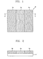
- FIG. 1 is a plan view showing sub-pixels constituting a single pixel of the related art LCD
- FIG. 2 is a sectional view of the sub-pixels constituting a single pixel of the LCD, taken along line II-II in FIG. 1 .
- the related art LCD includes a liquid crystal panel (not shown) that displays a desired image, and a backlight unit (not shown) that supplies light to the liquid crystal panel.
- the liquid crystal panel (not shown) includes an TFT array substrate (not shown) on which TFTs are formed, a color filter substrate (not shown) which is attached to the TFT array substrate and includes red (R), green (G) and blue (B) color filters, and a liquid crystal layer (not shown) filled between the TFT array substrate and the color filter substrate.
- a backlight unit of the LCD includes a plurality of lamps to provide light to the liquid crystal panel.
- three sub-pixels including red (R), green (G) and blue (B) color filters 13a, 17a and 21a constituting a single unit pixel 10 are formed on the color filter substrate.
- the color filters 13a, 17a and 21a will be considered to refer to the sub-pixels.
- the red (R), green (G) and blue (B) color filters 13a, 17a and 21a are arranged in a column direction.
- a black matrix layer (not shown) is formed to block light at boundaries of the red (R), green (G) and blue (B) color filters 13a, 17a and 21a.
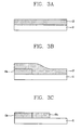
- FIGs. 3a to 3e are sectional views sequentially showing the process of fabricating sub-pixels constituting a single pixel of the related art LCD.
- a black matrix layer (not shown) is formed on the color filter substrate 11, a glass substrate, with ,an opaque material in order to prevent light transmission to other portions than the unit pixel area.
- one of a color, which is among red, green and blue, resin layer is coated on the color filter substrate 11 including the black matrix layer (not shown).
- the red color resin layer 13, among the red, green and blue color resin layers may be first coated.
- the red color resin layer 13 is selectively removed through exposing and developing processes using photolithography to form a red color resin layer pattern 13a.
- the red color resin layer pattern 13a is used as a red color filter and corresponds to the red sub-pixel.
- a green (G) color resin layer 17 is coated on the color filter substrate 11 including the red color resin layer pattern 13a.
- the green color resin layer 17 is selectively removed through exposing and developing processes using photolithography to form the green color resin layer pattern 17a.
- the green color resin layer pattern 17a is used as a green color filter and corresponds to the green sub-pixel.
- a blue (B) color resin layer 21 is coated on the color filter substrate 11 including the red and green color resin layer patterns 13a and 17a.
- the blue color resin layer 21 is selectively removed through exposing and developing processes using photolithography to form the blue color resin layer pattern 21a.
- the blue color resin layer pattern 21a is used as a blue color filter and corresponds to a blue sub-pixel.
- the color filters of the related art LCD fabricated as described above and the fabrication method have the following problems.
- One aspect of the exemplary embodiments is to provide a color filter of a liquid crystal display (LCD) capable of implementing six colors including red (R), green (G) and blue (B) without additional inks or processes by using complementary characteristics of the red (R), green (G) and blue (B), and its fabrication method.
- LCD liquid crystal display
- This specification provides an LCD including: a color filter substrate; and a plurality of pixels formed in a matrix form on the color filter substrate, each pixel including a first red sub-pixel, a first green sub-pixel, a first blue sub-pixel, a pair of second red sub-pixel and third green sub-pixel, a pair of second green sub-pixel and third blue sub-pixel, and a pair of second blue sub-pixel and third red sub-pixel.
- This specification also provides an LCD including: a thin film transistor (TFT) array substrate; a color filter substrate attached to the TFT array substrate; a plurality of pixels formed in a matrix form on the color filter substrate, each pixel including a first red sub-pixel, a first green sub-pixel, a first blue sub-pixel, a pair of second red sub-pixel and third green sub-pixel, a pair of second green sub-pixel and third blue sub-pixel, and a pair of second blue sub-pixel and third red sub-pixel; and a liquid crystal layer formed between the TFT array substrate and the color filter substrate.
- TFT thin film transistor
- This specification also provides a method for fabricating color filters of an LCD, including: providing a color filter substrate; and forming a plurality of pixels on the color filter substrate, wherein the forming of the plurality of pixels includes: forming first to third red sub-pixels on the color filter substrate; forming first to third green sub-pixels on other portions of the color filter substrate than the area where the first to third red sub-pixels have been formed; and forming first to third blue sub-pixels on other portions of the color filter substrate than the area where the first to third green sub-pixels and the first to third red sub-pixels have been formed.
- This specification also provides a method for fabricating an LCD, including: providing a color filter substrate; and forming a plurality of pixels on the color filter substrate, wherein the forming of the plurality of pixels includes: forming first to third red color resin layer patterns on the color filter substrate; forming first to third green sub-pixels on other portions of the color filter substrate than the area where the first to third red color resin layer patterns have been formed; and forming first to third blue color resin layer patterns on other portions of the color filter substrate than the area where the first to third green color resin layer patterns and the first to third red color resin layer patterns have been formed.
- FIG. 5 is an equivalent circuit diagram of a single sub-pixel of an LCD according to an exemplary embodiment of the present invention.
- FIG. 6 is a plan view of sub-pixels constituting a single pixel of the LCD according to an exemplary embodiment of the present invention.
- FIGs. 7a and 7b are sectional views constituting a single pixel of the LCD according to an exemplary embodiment of the present invention, wherein FIG. 7a is a sectional view taken along line VIIa-VIIa in FIG. 6, and FIG. 7b is a sectional view taken along line VIIb-VIIb in FIG. 6 .
- FIG. 8a to 8c are plan views for explaining the process of forming sub-pixels of a single pixel of the LCD according to an exemplary embodiment of the present invention.
- the LCD includes a liquid crystal panel including a thin film transistor (TFT) array substrate 101, a color filter substrate 201 with red (R), green (G) and blue (B) color filters formed thereon, and a liquid crystal layer (not shown) filled between the substrates, and a backlight unit (not shown) that provides light to the liquid crystal panel.
- TFT thin film transistor
- a plurality of gate lines Gm-1 and Gm and a plurality of data lines Dn are arranged to cross each other to form a sub-pixel area on the TFT array substrate 101, and a TFT (T), a switching element, is formed at each crossing of the gate lines and the data lines.
- T TFT
- a pixel electrode 109 is connected with the TFT (T) formed at each sub-pixel area.
- Each sub-pixel includes the TFT (T), the switching element, connected with the gate lines Gm-1 and Gm and the data line Dn, a liquid crystal capacitor Clc connected to the TFT (T), and a storage capacitor Cst.
- the storage capacitor may be omitted as necessary.
- the liquid crystal capacitor Clc uses the pixel electrode 109 of the lower array substrate 101 and a common electrode (not shown) of the upper color filter substrate 201 as two terminals, and the liquid crystal layer (not shown) between the two electrodes serves as a dielectric substance.
- the pixel electrode 109 is connected with the TFT (T), and the common electrode (not shown) is formed on the upper color filter substrate 201 and receives a common voltage Vcom.
- the common electrode (not shown) may be provided on the lower array substrate 101, and in this case, the pixel electrode 109 and the common electrode (not shown) may be formed in a linear or bar shape.
- the backlight unit (not shown) of the LCD includes a plurality of lamps to provide light to the liquid crystal panel.
- the lamps CCFLs (Cold Cathode Fluorescent Lamp), EEFLs (External Electrode Fluorescent Lamps), LEDs (Light Emitting Diodes), and the like, can be used.
- a plurality of pairs of sub-pixels that implement cyan (C), magenta (M) and yellow (Y) colors together with red (R), green (G), and blue (B) colors form a single pixel as a basic unit of an image.
- black matrixes are formed at boundaries of sub-pixels to prevent light transmission.
- the black matrixes are formed at boundaries of the respective sub-pixels in the following description.
- FIG. 6 is a plan view of sub-pixels constituting a single pixel of the LCD according to an exemplary embodiment of the present invention.
- FIGs. 7a and 7b are sectional views constituting a single pixel of the LCD according to an exemplary embodiment of the present invention, wherein FIG. 7a is a sectional view taken along line VIIa-VIIa in FIG. 6, and FIG. 7b is a sectional view taken along line VIIb-VIIb in FIG. 6 .
- the sub-pixels of a single pixel 200 of the color filters of the LCD has a basic structure of 1x6 matrix.
- the first, red (R), the first green (G) and the first blue (B) sub-pixels 203a, 205a and 207a are disposed at the three rows, and pairs of sub-pixels are formed at the remaining rows in a 2x3 matrix form.
- a second red sub-pixel 203b and a third green sup-pixel 205c make a pair in a first column
- a second green sub-pixel 20b and a third blue sub-pixel 207c make a pair in a second column
- a second blue sub-pixel 207b and a third red sub-pixel 203c make a pair in a third column.
- the pair of second red sub-pixel 203b and the third green sub-pixel 205c implement yellow color
- the pair of second green sub-pixel 205b and third blue sub-pixel 207c implement cyan color
- the pair of second blue sub-pixel 207b and third red sub-pixel 203c implement magenta color.
- red, green, blue, cyan, magenta and yellow colors are implemented by the nine sub-pixels (namely, color filters) constituting the single pixel 200.
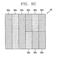
- FIG. 8a to 8c are plan views for explaining the process of forming sub-pixels of a single pixel of the LCD according to an exemplary embodiment of the present invention.
- red, green and blue color filter resin layers not shown are coated on the color filter substrate 201.
- a red color resin layer 13, among the red, green and blue color resin layers, is first coated will be taken as an example.
- color resin layer major components of the color resin layer include photopolymerization type photosensitive composition such as a photopolymerization initiator, monomer, a binder, and organic pigments assuming R, G and B and their similar colors.
- photopolymerization type photosensitive composition such as a photopolymerization initiator, monomer, a binder, and organic pigments assuming R, G and B and their similar colors.
- a black matrix layer (not shown) is formed with an opaque material to prevent light from transmitting through other portions than unit pixel areas on the color filter substrate 201 at a previous stage before the red color resin layer is coated.
- the black matrix is formed at boundaries of the respective sub-pixels in the following description.
- the red color resin layer (not shown) is selectively removed through exposing and developing processes using photolithography to form red color resin layer patterns 203a, 203b and 203c.
- the red color resin layer patterns 203a, 203b and 230c are used as the first to third red sub-pixels 203a, 203b and 230c.
- the second and third red sub-pixels 203b and 203c are disposed in columns different from that of the first red sub-pixel 203a, and respectively have an area corresponding to a half of or smaller than that of the first red sub-pixel 203a.
- a green color resin layer (not shown) is formed on the color filter substrate 201 including the red color resin layer patterns 203a, 230b and 203c.
- the green color resin layer (not shown) is selectively removed through exposing and developing processes using photolithography to form green color resin layer patterns 205a, 205b and 205c.
- the green color resin layer patterns 205a, 205b and 205c can be used as first to third green sub-pixels 205a, 205b and 205c.
- the second and third green sub-pixels 205b and 205c are disposed in columns different from that of the first green sub-pixel 205a and respectively have an area corresponding to a half of or smaller than that of the first green sub-pixel 205a.
- the green sub-pixels 205a, 205b and 205c do not overlap with the red sub-pixels 203a, 203b and 203c.
- the second green sub-pixel 205b is disposed in the a different column from that of the second red sub-pixel 203b, and the third green sub-pixel 205c is disposed in the same column as the second red sub-pixel 203b.
- the third green sub-pixel 205c and the second red sub-pixel 203b disposed in the same column implement the yellow color.
- a blue color resin layer (not shown) is formed on the color filter substrate 201 including the red color resin layer patterns 203a, 203b and 203c and the green color resin layer patterns 205a, 205b and 205c.
- the blue color resin layer (not shown) is selectively removed through exposing and developing processes using photolithography to form the blue color resin layer patterns 207a, 207b and 207c, thus completing formation of the plurality of sub-pixels constituting a single pixel.
- the red color resin layer patterns 207a, 207b and 207c are used as first to third blue sub-pixels 207a, 207b and 207c.
- the blue sub-pixels 207a, 207b and 207c do not overlap with the red sub-pixels 203a, 203b and 203c and the green sub-pixels 205a, 205b and 205c.
- the second blue sub-pixel 207b is disposed in the same column in which the third red sub-pixel 203c is disposed, and the third blue sub-pixel 207c is disposed in the same column in which the second green sub-pixel 205b is disposed.
- the second blue sub-pixel 207b and the red sub-pixel 203c disposed in the same column implement a magenta color
- the third blue sub-pixel 207c and the second green sub-pixel 205b disposed in the same column implement a cyan color.
- the triangle in the color coordinates indicates a general color coordinates, and because cyan (C), magenta (M) and yellow (Y) color coordinates are added, every color within the hexagon can be implemented.
- a gate metallic material is deposited on an insulation substrate made of transparent glass to form a gate metallic film, and the gate metallic film is selectively patterned through a masking process to form gate lines and gate electrodes protruded from the gate lines.
- a aluminum-based metal such as Al, an Al alloy, etc.
- a silver -based metal such as Ag, an Ag alloy, etc.
- a molybdenum-based metal such as Mo, an Mo alloy, etc., Cr, Ti, Ta, etc.
- the gate metallic film may include two layers each having different physical properties, namely, a lower layer and an upper layer.
- the upper layer may be made of a metal with low resistivity, such as an aluminum-based metal or silver-based metal, in order to reduce a signal delay or a voltage drop of the gate line.
- the lower layer may be made of a different material, in particular, a material having good physical, chemical and electrical contact characteristics with ITO (Indium Tin Oxide) or IZO (Indium Zinc Oxide).
- the lower layer may be made of Ti, Ta, Cr, Mo-based metal, etc.
- the combination of the lower layer and the upper layer can be, for example, a Cr/Al-Nd alloy.
- a semiconductor layer made of hydrogenated amorphous silicon, etc., is formed on the gate insulating layer.
- an ohmic contact layer made of a material such as n+ hydrogenated amorphous silicon, etc., in which silicide or 'n' type impurities are doped with a high density, is formed on the semiconductor layer.
- the ohmic contact layer and the semiconductor layer are selectively patterned through a masking process.
- a metallic material for data lines is deposited on the insulation substrate including the selectively patterned ohmic contact layer and semiconductor layer to form a metallic film for data lines, and the metallic film for data lies is then selectively patterned through a masking process to form a data line, a source electrode protruded from the data line, and a drain electrode spaced apart from the source electrode.
- the data line and the gate line are formed to cross each other, and the source electrode and the drain electrode form the TFT, the switching element, together with the lower gate electrode.
- a channel of the TFT is formed at the semiconductor layer between the source electrode and the drain electrode.
- the metallic film for data lines can be made of an aluminum-based metal, a silver-based metal, a molybdenum-based metal, Cr, Ti, Ta, etc., and may be formed as a multi-layer.
- the protection layer is selectively patterned through a masking process to form a contact hole exposing a portion of the drain electrode in the protection layer.
- a metallic material layer made of a transparent conductive material such as ITO or IZO or a reflective metal is deposited on the protection layer including the contact hole, and then selectively removed through a masking process to form a plurality of pixel electrodes.
- the pixel electrodes when data voltage is applied to the pixel electrodes, the pixel electrodes generate an electric field together with the common electrode of the upper color filter substrate which has been received a common voltage, to thus arrange liquid crystal molecules of the liquid crystal layer between the pixel electrodes and the common electrode.
- the common electrode is formed on the upper color filter substrate, and as mentioned above, it may be also formed on the lower insulation substrate as necessary.
- the color filters of the LCD and its fabrication method according to the present invention have the following advantages.
- the six colors can be implemented without performing additional color filter forming process and masking process.
- the fabrication cost can be reduced and the color reproduction characteristics can be improved.
Landscapes
- Physics & Mathematics (AREA)
- Nonlinear Science (AREA)
- General Physics & Mathematics (AREA)
- Optics & Photonics (AREA)
- Mathematical Physics (AREA)
- Chemical & Material Sciences (AREA)
- Crystallography & Structural Chemistry (AREA)
- Liquid Crystal (AREA)
- Optical Filters (AREA)
- Devices For Indicating Variable Information By Combining Individual Elements (AREA)
Abstract
Description
- The present invention relates to a color filter of a liquid crystal display (LCD) and, more particularly, to a color filter of an LCD that can implement 6 primary colors by adding cyan (C), magenta (M) and yellow (Y) complementary colors to a color reproduction range using the existing red (R), green (G) and blue (B).
- In general, the LCD includes two display panels and a liquid crystal layer, which has dielectric anisotropy, interposed between the two display panels.
- In the LCD, an electric field is applied to the liquid crystal layer, and the strength of the electric field is controlled to adjust transmittance of light that passes through the liquid crystal layer to obtain a desired image.
- The LCD is a typical device among portable flat panel displays (FPDs), and a thin film transistor (TFT) LCD including TFTs as switching elements is commonly used.
- The LCD includes a plurality of sub-pixels including pixel electrodes (not shown) and red, green and blue color filters.
- Each sub-pixel is driven by a signal applied via a display signal line to perform a display operation.
- Signal lines include gate lines (or scan signal lines0 that transfer scan signals and data lines that transfer data signals. Each sub-pixel includes a TFT which is connected with a single gate line and a single data line, through which an image signal transferred to a pixel electrode formed in the sub-pixel is controlled.
- In the related art LCD, the red (R), green (G) and blue (B) color filters are arranged in various forms.
- That is, in a stripe type color filter arrangement, the same color filters are arranged in units of sub-pixel rows. In a mosaic type color filter arrangement, the red (R), green (G) and blue (B) color filters are sequentially arranged in rows and columns. In a delta type color filter arrangement, sub-pixels are disposed in zigzags in a column direction, and red (R), green (G) and blue (B) color filters are sequentially arranged.
- The related art LCD using the delta-type color filter arrangement method will now be described with reference to
FIG. 1 and 2 . -
FIG. 1 is a plan view showing sub-pixels constituting a single pixel of the related art LCD, andFIG. 2 is a sectional view of the sub-pixels constituting a single pixel of the LCD, taken along line II-II inFIG. 1 . - Although not shown< the related art LCD includes a liquid crystal panel (not shown) that displays a desired image, and a backlight unit (not shown) that supplies light to the liquid crystal panel.
- Here the liquid crystal panel (not shown) includes an TFT array substrate (not shown) on which TFTs are formed, a color filter substrate (not shown) which is attached to the TFT array substrate and includes red (R), green (G) and blue (B) color filters, and a liquid crystal layer (not shown) filled between the TFT array substrate and the color filter substrate.
- A backlight unit of the LCD includes a plurality of lamps to provide light to the liquid crystal panel.
- With reference to
FIG. 1 , three sub-pixels including red (R), green (G) and blue (B)color filters single unit pixel 10 are formed on the color filter substrate. Here, thecolor filters - The red (R), green (G) and blue (B)
color filters - A black matrix layer (not shown) is formed to block light at boundaries of the red (R), green (G) and blue (B)
color filters - The method for fabricating the color filters of the LCD according to the related art having such array structure will now be described with reference to
FIGs. 3a to 3e . -
FIGs. 3a to 3e are sectional views sequentially showing the process of fabricating sub-pixels constituting a single pixel of the related art LCD. - With reference to
FIG. 3 , first, a black matrix layer (not shown) is formed on thecolor filter substrate 11, a glass substrate, with ,an opaque material in order to prevent light transmission to other portions than the unit pixel area. - Next, one of a color, which is among red, green and blue, resin layer is coated on the
color filter substrate 11 including the black matrix layer (not shown). Here, for example, the redcolor resin layer 13, among the red, green and blue color resin layers, may be first coated. - And then, the red
color resin layer 13 is selectively removed through exposing and developing processes using photolithography to form a red colorresin layer pattern 13a. In this case, the red colorresin layer pattern 13a is used as a red color filter and corresponds to the red sub-pixel. - Subsequently, as shown in
FIG. 3b , a green (G)color resin layer 17 is coated on thecolor filter substrate 11 including the red colorresin layer pattern 13a. - And then, as shown in
FIG. 3c , the greencolor resin layer 17 is selectively removed through exposing and developing processes using photolithography to form the green colorresin layer pattern 17a. In this case, the green colorresin layer pattern 17a is used as a green color filter and corresponds to the green sub-pixel. - Thereafter, as shown in
FIG .3d , a blue (B)color resin layer 21 is coated on thecolor filter substrate 11 including the red and green colorresin layer patterns - And then, as shown in
FIG. 3e , the bluecolor resin layer 21 is selectively removed through exposing and developing processes using photolithography to form the blue colorresin layer pattern 21a. In this case, the blue colorresin layer pattern 21a is used as a blue color filter and corresponds to a blue sub-pixel. - The color filters of the related art LCD fabricated as described above and the fabrication method have the following problems.
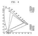
- That is, in the color filters of the related art LCD and its fabrication method, only the three R, G and B colors are used to form the color filters, and as shown in
FIG. 4 , formation of the color filters with three colors has a limitation in implementing color reproduction characteristics close to the natural colors. - Thus, a method of adding three cyan, magenta and yellow color filters to the three R, G and B color filters has been proposed, which, however, has failed to be employed for mass production because it incurs high fabrication costs for development of additional color inks (cyan, magenta and yellow) and an additional photo process.
- Therefore, in order to address the above matters the various features described herein have been conceived. One aspect of the exemplary embodiments is to provide a color filter of a liquid crystal display (LCD) capable of implementing six colors including red (R), green (G) and blue (B) without additional inks or processes by using complementary characteristics of the red (R), green (G) and blue (B), and its fabrication method.
- This specification provides an LCD including: a color filter substrate; and a plurality of pixels formed in a matrix form on the color filter substrate, each pixel including a first red sub-pixel, a first green sub-pixel, a first blue sub-pixel, a pair of second red sub-pixel and third green sub-pixel, a pair of second green sub-pixel and third blue sub-pixel, and a pair of second blue sub-pixel and third red sub-pixel.
- This specification also provides an LCD including: a thin film transistor (TFT) array substrate; a color filter substrate attached to the TFT array substrate; a plurality of pixels formed in a matrix form on the color filter substrate, each pixel including a first red sub-pixel, a first green sub-pixel, a first blue sub-pixel, a pair of second red sub-pixel and third green sub-pixel, a pair of second green sub-pixel and third blue sub-pixel, and a pair of second blue sub-pixel and third red sub-pixel; and a liquid crystal layer formed between the TFT array substrate and the color filter substrate.
- This specification also provides a method for fabricating color filters of an LCD, including: providing a color filter substrate; and forming a plurality of pixels on the color filter substrate, wherein the forming of the plurality of pixels includes: forming first to third red sub-pixels on the color filter substrate; forming first to third green sub-pixels on other portions of the color filter substrate than the area where the first to third red sub-pixels have been formed; and forming first to third blue sub-pixels on other portions of the color filter substrate than the area where the first to third green sub-pixels and the first to third red sub-pixels have been formed.
- This specification also provides a method for fabricating an LCD, including: providing a color filter substrate; and forming a plurality of pixels on the color filter substrate, wherein the forming of the plurality of pixels includes: forming first to third red color resin layer patterns on the color filter substrate; forming first to third green sub-pixels on other portions of the color filter substrate than the area where the first to third red color resin layer patterns have been formed; and forming first to third blue color resin layer patterns on other portions of the color filter substrate than the area where the first to third green color resin layer patterns and the first to third red color resin layer patterns have been formed.
- The foregoing and other objects, features, aspects and advantages of the present invention will become more apparent from the following detailed description of the present invention when taken in conjunction with the accompanying drawings.
-
-
FIG. 1 is a plan view showing sub-pixels constituting a single pixel of a liquid crystal display (LCD) according to the related art; -
FIG. 2 is a sectional view of the sub-pixels constituting a single pixel of the LCD, taken along line II-II inFIG. 1 ; -
FIGs. 3a to 3e are sectional views sequentially showing the process of fabricating sub-pixels of a single pixel of the LCD according to the related art; -
FIG. 4 is a graph showing a color coordinate of a color filter of the LCD according to the related art; -
FIG. 5 is an equivalent circuit diagram of a single sub-pixel of an LCD according to an exemplary embodiment of the present invention; -
FIG. 6 is a plan view of sub-pixels constituting a single pixel of the LCD according to an exemplary embodiment of the present invention; -
FIGs. 7a and 7b are sectional views constituting a single pixel of the LCD according to an exemplary embodiment of the present invention, wherein-
FIG. 7a is a sectional view taken along line VIIa-VIIa inFIG. 6 ; and -
FIG. 7b is a sectional view taken along line Vllb-Vllb inFIG. 6 .
-
-
FIG. 8a to 8c are plan views for explaining the process of forming sub-pixels of a single pixel of the LCD according to an exemplary embodiment of the present invention; and -
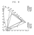
FIG. 9 is a graph showing a color coordinate of a color filter of the LCD according to an exemplary embodiment of the present invention. - Color filters of a liquid crystal display (LCD) and its fabrication method according to an exemplary embodiment of the present invention will now be described in detail with reference to the accompanying drawings.
-
FIG. 5 is an equivalent circuit diagram of a single sub-pixel of an LCD according to an exemplary embodiment of the present invention. -
FIG. 6 is a plan view of sub-pixels constituting a single pixel of the LCD according to an exemplary embodiment of the present invention. -
FIGs. 7a and 7b are sectional views constituting a single pixel of the LCD according to an exemplary embodiment of the present invention, whereinFIG. 7a is a sectional view taken along line VIIa-VIIa inFIG. 6, and FIG. 7b is a sectional view taken along line VIIb-VIIb inFIG. 6 . -
FIG. 8a to 8c are plan views for explaining the process of forming sub-pixels of a single pixel of the LCD according to an exemplary embodiment of the present invention. - With reference to
FIG. 5 , the LCD according to an exemplary embodiment of the present invention includes a liquid crystal panel including a thin film transistor (TFT)array substrate 101, acolor filter substrate 201 with red (R), green (G) and blue (B) color filters formed thereon, and a liquid crystal layer (not shown) filled between the substrates, and a backlight unit (not shown) that provides light to the liquid crystal panel. - A plurality of gate lines Gm-1 and Gm and a plurality of data lines Dn are arranged to cross each other to form a sub-pixel area on the
TFT array substrate 101, and a TFT (T), a switching element, is formed at each crossing of the gate lines and the data lines. - A
pixel electrode 109 is connected with the TFT (T) formed at each sub-pixel area. - Each sub-pixel includes the TFT (T), the switching element, connected with the gate lines Gm-1 and Gm and the data line Dn, a liquid crystal capacitor Clc connected to the TFT (T), and a storage capacitor Cst. In this case, the storage capacitor may be omitted as necessary.
- The liquid crystal capacitor Clc uses the
pixel electrode 109 of thelower array substrate 101 and a common electrode (not shown) of the uppercolor filter substrate 201 as two terminals, and the liquid crystal layer (not shown) between the two electrodes serves as a dielectric substance. - The
pixel electrode 109 is connected with the TFT (T), and the common electrode (not shown) is formed on the uppercolor filter substrate 201 and receives a common voltage Vcom. - The common electrode (not shown) may be provided on the
lower array substrate 101, and in this case, thepixel electrode 109 and the common electrode (not shown) may be formed in a linear or bar shape. - The backlight unit (not shown) of the LCD includes a plurality of lamps to provide light to the liquid crystal panel. In this case, as the lamps, CCFLs (Cold Cathode Fluorescent Lamp), EEFLs (External Electrode Fluorescent Lamps), LEDs (Light Emitting Diodes), and the like, can be used.
- On the color filter substrates, a plurality of pairs of sub-pixels that implement cyan (C), magenta (M) and yellow (Y) colors together with red (R), green (G), and blue (B) colors form a single pixel as a basic unit of an image.
- Although not shown, black matrixes are formed at boundaries of sub-pixels to prevent light transmission. Here, it is assumed that the black matrixes are formed at boundaries of the respective sub-pixels in the following description.
- The disposition structure and disposition method of sub-pixels of the color filter substrates of the LCD according to an exemplary embodiment of the present invention will now be described in detail.
-
FIG. 6 is a plan view of sub-pixels constituting a single pixel of the LCD according to an exemplary embodiment of the present invention. -
FIGs. 7a and 7b are sectional views constituting a single pixel of the LCD according to an exemplary embodiment of the present invention, whereinFIG. 7a is a sectional view taken along line VIIa-VIIa inFIG. 6, and FIG. 7b is a sectional view taken along line VIIb-VIIb inFIG. 6 . - With reference to
FIGs. 6 and 7a and 7b , the sub-pixels of asingle pixel 200 of the color filters of the LCD according to an exemplary embodiment of the present invention has a basic structure of 1x6 matrix. Of the sub-pixels, the first, red (R), the first green (G) and the first blue (B) sub-pixels 203a, 205a and 207a are disposed at the three rows, and pairs of sub-pixels are formed at the remaining rows in a 2x3 matrix form. - In detail, in the 2x3 matrix form, a second
red sub-pixel 203b and a third green sup-pixel 205c make a pair in a first column, a second green sub-pixel 20b and a thirdblue sub-pixel 207c make a pair in a second column, and a secondblue sub-pixel 207b and a thirdred sub-pixel 203c make a pair in a third column. - Here, the pair of second
red sub-pixel 203b and the thirdgreen sub-pixel 205c implement yellow color, the pair of secondgreen sub-pixel 205b and thirdblue sub-pixel 207c implement cyan color, and the pair of secondblue sub-pixel 207b and thirdred sub-pixel 203c implement magenta color. - In this manner the red, green, blue, cyan, magenta and yellow colors are implemented by the nine sub-pixels (namely, color filters) constituting the
single pixel 200. - The method for forming a plurality of sub-pixels constituting a single pixel of the color filter will now be described with reference to
FIGs. 8a to 8c . -
FIG. 8a to 8c are plan views for explaining the process of forming sub-pixels of a single pixel of the LCD according to an exemplary embodiment of the present invention. - Although not shown, one of red, green and blue color filter resin layers not shown) is coated on the
color filter substrate 201. Here, a case where a redcolor resin layer 13, among the red, green and blue color resin layers, is first coated will be taken as an example. - In this case, major components of the color resin layer include photopolymerization type photosensitive composition such as a photopolymerization initiator, monomer, a binder, and organic pigments assuming R, G and B and their similar colors.
- Although not shown, a black matrix layer (not shown) is formed with an opaque material to prevent light from transmitting through other portions than unit pixel areas on the
color filter substrate 201 at a previous stage before the red color resin layer is coated. Here, it is assumed that the black matrix is formed at boundaries of the respective sub-pixels in the following description. - Subsequently, with reference to
FIG. 8a , the red color resin layer (not shown) is selectively removed through exposing and developing processes using photolithography to form red colorresin layer patterns resin layer patterns - Among the sub-pixels 203a, 203b and 203c, the second and third red sub-pixels 203b and 203c are disposed in columns different from that of the first
red sub-pixel 203a, and respectively have an area corresponding to a half of or smaller than that of the firstred sub-pixel 203a. - Thereafter, although not shown, a green color resin layer (not shown) is formed on the
color filter substrate 201 including the red colorresin layer patterns - And then, as shown in
FIG. 8b , the green color resin layer (not shown) is selectively removed through exposing and developing processes using photolithography to form green colorresin layer patterns resin layer patterns green sub-pixels - Among the green sub-pixels 205a, 205b and 205c, the second and third
green sub-pixels green sub-pixel 205a and respectively have an area corresponding to a half of or smaller than that of the firstgreen sub-pixel 205a. - The green sub-pixels 205a, 205b and 205c do not overlap with the red sub-pixels 203a, 203b and 203c.
- The second
green sub-pixel 205b is disposed in the a different column from that of the secondred sub-pixel 203b, and the thirdgreen sub-pixel 205c is disposed in the same column as the secondred sub-pixel 203b. The thirdgreen sub-pixel 205c and the secondred sub-pixel 203b disposed in the same column implement the yellow color. - Subsequently, although not shown, a blue color resin layer (not shown) is formed on the
color filter substrate 201 including the red colorresin layer patterns resin layer patterns - And then, as shown in
FIG. 8c , the blue color resin layer (not shown) is selectively removed through exposing and developing processes using photolithography to form the blue colorresin layer patterns - In this case, the red color
resin layer patterns - The blue sub-pixels 207a, 207b and 207c do not overlap with the red sub-pixels 203a, 203b and 203c and the green sub-pixels 205a, 205b and 205c.
- The second
blue sub-pixel 207b is disposed in the same column in which the thirdred sub-pixel 203c is disposed, and the thirdblue sub-pixel 207c is disposed in the same column in which the secondgreen sub-pixel 205b is disposed. - The second
blue sub-pixel 207b and thered sub-pixel 203c disposed in the same column implement a magenta color, and the thirdblue sub-pixel 207c and the secondgreen sub-pixel 205b disposed in the same column implement a cyan color. - By disposing the nine sub-pixels constituting a single pixel in such manners, a change in six color coordinates of the LCD as shown in
FIG. 9 can be recognized. - Namely, in
FIG. 9 , the triangle in the color coordinates indicates a general color coordinates, and because cyan (C), magenta (M) and yellow (Y) color coordinates are added, every color within the hexagon can be implemented. - A method for fabricating the TFTs on the array substrate which is to be attached to the color filter substrate on which a plurality of sub-pixels are formed will now be described.
- Although not shown, a gate metallic material is deposited on an insulation substrate made of transparent glass to form a gate metallic film, and the gate metallic film is selectively patterned through a masking process to form gate lines and gate electrodes protruded from the gate lines.
- In this case, as the gate metallic material, a aluminum-based metal such as Al, an Al alloy, etc., a silver -based metal such as Ag, an Ag alloy, etc., a molybdenum-based metal such as Mo, an Mo alloy, etc., Cr, Ti, Ta, etc.
- In addition, the gate metallic film may include two layers each having different physical properties, namely, a lower layer and an upper layer. The upper layer may be made of a metal with low resistivity, such as an aluminum-based metal or silver-based metal, in order to reduce a signal delay or a voltage drop of the gate line.
- The lower layer may be made of a different material, in particular, a material having good physical, chemical and electrical contact characteristics with ITO (Indium Tin Oxide) or IZO (Indium Zinc Oxide). For example, the lower layer may be made of Ti, Ta, Cr, Mo-based metal, etc. The combination of the lower layer and the upper layer can be, for example, a Cr/Al-Nd alloy.
- Next, a gate insulating layer made of silicon nitride (SiNx), etc., is formed on the insulation substrate including the gate lines and the gate electrodes.
- Subsequently, a semiconductor layer made of hydrogenated amorphous silicon, etc., is formed on the gate insulating layer.
- And then, an ohmic contact layer made of a material such as n+ hydrogenated amorphous silicon, etc., in which silicide or 'n' type impurities are doped with a high density, is formed on the semiconductor layer.
- Thereafter, the ohmic contact layer and the semiconductor layer are selectively patterned through a masking process.
- And then, a metallic material for data lines is deposited on the insulation substrate including the selectively patterned ohmic contact layer and semiconductor layer to form a metallic film for data lines, and the metallic film for data lies is then selectively patterned through a masking process to form a data line, a source electrode protruded from the data line, and a drain electrode spaced apart from the source electrode.
- The data line and the gate line are formed to cross each other, and the source electrode and the drain electrode form the TFT, the switching element, together with the lower gate electrode. A channel of the TFT is formed at the semiconductor layer between the source electrode and the drain electrode.
- The metallic film for data lines can be made of an aluminum-based metal, a silver-based metal, a molybdenum-based metal, Cr, Ti, Ta, etc., and may be formed as a multi-layer.
- A protection layer made of an organic material having good planarization characteristics and photosensitivity, an insulation material having low dielectric constant characteristics, or silicon nitride, an in organic material, etc., is formed on the insulation substrate including the data line and the drain electrode.
- And then, the protection layer is selectively patterned through a masking process to form a contact hole exposing a portion of the drain electrode in the protection layer.
- Thereafter, a metallic material layer made of a transparent conductive material such as ITO or IZO or a reflective metal is deposited on the protection layer including the contact hole, and then selectively removed through a masking process to form a plurality of pixel electrodes. In this case, when data voltage is applied to the pixel electrodes, the pixel electrodes generate an electric field together with the common electrode of the upper color filter substrate which has been received a common voltage, to thus arrange liquid crystal molecules of the liquid crystal layer between the pixel electrodes and the common electrode.
- In the above description, the common electrode is formed on the upper color filter substrate, and as mentioned above, it may be also formed on the lower insulation substrate as necessary.
- The color filters of the LCD and its fabrication method according to the present invention have the following advantages.
- First, because a plurality of sub-pixels constituting a single pixel are disposed in each different columns and in the same columns to add cyan (C), magenta (M) and yellow (Y) colors to the red (R), green (G) and blue (B) colors, the hexagon of six colors can be implemented, so color reproduction close to the natural colors can be implemented.
- In particular, because the cyan (C), magenta (M) and yellow (Y) colors are implemented by using the complementary characteristics of red (R), green (G) and blue (B) colors, the six colors can be implemented without performing additional color filter forming process and masking process.
- Therefore, because the six colors can be implemented without any additional process, the fabrication cost can be reduced and the color reproduction characteristics can be improved.
- As the present invention may be embodied in several forms without departing from the characteristics thereof, it should also be understood that the above-described embodiments are not limited by any of the details of the foregoing description, unless otherwise specified, but rather should be construed broadly within its scope as defined in the appended claims, and therefore all changes and modifications that fall within the metes and bounds of the claims, or equivalents of such metes and bounds are therefore intended to be embraced by the appended claims.
Claims (20)
- A liquid crystal display device, comprising:a color filter substrate; anda plurality of pixels formed in a matrix form on the color filter substrate, each pixel including a first red sub-pixel, a first green sub-pixel, a first blue sub-pixel, a pair of second red sub-pixel and third green sub-pixel, a pair of second green sub-pixel and third blue sub-pixel, and a pair of second blue sub-pixel and third red sub-pixel.
- The device of claim 1, wherein the first red sub-pixel, the first green sub-pixel and the first blue sub-pixel are disposed in different columns.
- The device of claim 1, wherein the pair of second red sub-pixel and third green sub-pixel, the pair of second green sub-pixel and third blue sub-pixel, and the pair of second blue sub-pixel and third red sub-pixel are disposed in different columns.
- The device of claim 1, wherein the pair of second red sub-pixel and third green sub-pixel, the pair of second green sub-pixel and third blue sub-pixel, and the pair of second blue sub-pixel and third red sub-pixel are disposed in the same columns.
- The device of claim 1, wherein the pair of second red sub-pixel and third green sub-pixel implement yellow (Y) color, the pair of second green sub-pixel and third blue sub-pixel implement cyan (C) color, and the pair of second blue sub-pixel and third red sub-pixel implement magenta (M) color.
- A liquid crystal display device comprising:a thin film transistor (TFT) array substrate;a color filter substrate attached to the TFT array substrate;a plurality of pixels formed in a matrix form on the color filter substrate, each pixel including a first red sub-pixel, a first green sub-pixel, a first blue sub-pixel, a pair of second red sub-pixel and third green sub-pixel, a pair of second green sub-pixel and third blue sub-pixel, and a pair of second blue sub-pixel and third red sub-pixel; anda liquid crystal layer formed between the TFT array substrate and the color filter substrate.
- The device of claim 6, wherein the first red sub-pixel, the first green sub-pixel and the first blue sub-pixel are disposed in different columns.
- The device of claim 6, wherein the pair of second red sub-pixel and third green sub-pixel, the pair of second green sub-pixel and third blue sub-pixel, and the pair of second blue sub-pixel and third red sub-pixel are disposed in different columns.
- The device of claim 6, wherein the pair of second red sub-pixel and third green sub-pixel, the pair of second green sub-pixel and third blue sub-pixel, and the pair of second blue sub-pixel and third red sub-pixel are disposed in the same columns.
- The color filters of claim 6, wherein the pair of second red sub-pixel and third green sub-pixel implement yellow (Y) color, the pair of second green sub-pixel and third blue sub-pixel implement cyan (C) color, and the pair of second blue sub-pixel and third red sub-pixel implement magenta (M) color.
- A method for fabricating color filters of a liquid crystal display, comprising:providing a color filter substrate; andforming a plurality of pixels on the color filter substrate,
wherein the forming of the plurality of pixels comprises:forming first to third red sub-pixels on the color filter substrate;forming first to third green sub-pixels on other portions of the color filter substrate than the area where the first to third red sub-pixels have been formed; andforming first to third blue sub-pixels on other portions of the color filter substrate than the area where the first to third green sub-pixels and the first to third red sub-pixels have been formed. - The method of claim 11, wherein the first red sub-pixel, the first green sub-pixel and the first blue sub-pixel are disposed in different columns.
- The method of claim 11, wherein the pair of second red sub-pixel and third green sub-pixel, the pair of second green sub-pixel and third blue sub-pixel, and the pair of second blue sub-pixel and third red sub-pixel are disposed in different columns.
- The method of claim 13, wherein the pair of second red sub-pixel and third green sub-pixel, the pair of second green sub-pixel and third blue sub-pixel, and the pair of second blue sub-pixel and third red sub-pixel are disposed in the same columns.
- The method of claim 11, wherein the pair of second red sub-pixel and third green sub-pixel implement yellow (Y) color, the pair of second green sub-pixel and third blue sub-pixel implement cyan (C) color, and the pair of second blue sub-pixel and third red sub-pixel implement magenta (M) color.
- A method for fabricating color filters of a liquid crystal display, comprising:providing a color filter substrate; andforming a plurality of pixels on the color filter substrate,
wherein the forming of the plurality of pixels comprises:forming first to third red color resin layer patterns on the color filter substrate;forming first to third green sub-pixels on other portions of the color filter substrate than the area where the first to third red color resin layer patterns have been formed; andforming first to third blue color resin layer patterns on other portions of the color filter substrate than the area where the first to third green color resin layer patterns and the first to third red color resin layer patterns have been formed. - The method of claim 16, wherein the first red color resin layer pattern, the first green color resin layer pattern and the first blue color resin layer pattern are disposed in different columns.
- The method of claim 16, wherein the pair of second red color resin layer pattern and third green color resin layer pattern, the pair of second green color resin layer pattern and third blue color resin layer pattern, and the pair of second blue color resin layer pattern and third red color resin layer pattern are disposed in different columns.
- The method of claim 18, wherein the pair of second red color resin layer pattern and third green color resin layer pattern, the pair of second green color resin layer pattern and third blue color resin layer pattern, and the pair of second blue color resin layer pattern and third red color resin layer pattern are disposed in the same columns.
- The color filters of claim 1, wherein the pair of second red color resin layer pattern and third green color resin layer pattern implement yellow (Y) color, the pair of second green color resin layer pattern and third blue color resin layer pattern implement cyan (C) color, and the pair of second blue color resin layer pattern and third red color resin layer pattern implement magenta (M) color.
Applications Claiming Priority (1)
| Application Number | Priority Date | Filing Date | Title |
|---|---|---|---|
| KR1020070025111A KR20080084034A (en) | 2007-03-14 | 2007-03-14 | Color filter and manufacturing method of liquid crystal display |
Publications (3)
| Publication Number | Publication Date |
|---|---|
| EP1970750A2 true EP1970750A2 (en) | 2008-09-17 |
| EP1970750A3 EP1970750A3 (en) | 2009-09-23 |
| EP1970750B1 EP1970750B1 (en) | 2016-08-17 |
Family
ID=39373099
Family Applications (1)
| Application Number | Title | Priority Date | Filing Date |
|---|---|---|---|
| EP08004721.0A Active EP1970750B1 (en) | 2007-03-14 | 2008-03-13 | Color filters of liquid crystal display and method for fabricating the same |
Country Status (6)
| Country | Link |
|---|---|
| US (1) | US7911566B2 (en) |
| EP (1) | EP1970750B1 (en) |
| JP (1) | JP2008225481A (en) |
| KR (1) | KR20080084034A (en) |
| CN (1) | CN101266356A (en) |
| TW (1) | TWI382376B (en) |
Families Citing this family (11)
| Publication number | Priority date | Publication date | Assignee | Title |
|---|---|---|---|---|
| TWI439738B (en) * | 2011-07-01 | 2014-06-01 | E Ink Holdings Inc | Color filter and color display device with the same |
| CN103257494B (en) * | 2013-04-27 | 2016-03-30 | 北京京东方光电科技有限公司 | Display base plate and display device |
| TWI574078B (en) | 2014-12-02 | 2017-03-11 | 聯詠科技股份有限公司 | Display device and driving module thereof |
| TWI587041B (en) | 2014-12-02 | 2017-06-11 | 聯詠科技股份有限公司 | Display device and driving module thereof |
| TWI556048B (en) * | 2014-12-02 | 2016-11-01 | 聯詠科技股份有限公司 | Display device and driving module thereof |
| KR102508727B1 (en) * | 2015-11-19 | 2023-03-14 | 삼성디스플레이 주식회사 | Display device |
| CN106873236B (en) * | 2017-04-11 | 2019-11-29 | 惠科股份有限公司 | Display panel manufacturing method and display panel |
| CN107065294A (en) * | 2017-06-29 | 2017-08-18 | 京东方科技集团股份有限公司 | Color membrane substrates and preparation method, display panel |
| CN107799013B (en) * | 2017-10-30 | 2020-04-24 | 武汉天马微电子有限公司 | Display panel, display screen and display device |
| CN211786494U (en) * | 2019-12-27 | 2020-10-27 | 深圳Tcl数字技术有限公司 | A backlight module and liquid crystal display |
| CN115267961B (en) * | 2022-08-25 | 2024-05-24 | 济南大学 | Ultrathin color filter based on effective medium theory and preparation method thereof |
Citations (1)
| Publication number | Priority date | Publication date | Assignee | Title |
|---|---|---|---|---|
| US20070008462A1 (en) | 2005-07-08 | 2007-01-11 | Samsung Electronics Co., Ltd. | Color filter substrate, method of manufacturing the same and display apparatus having the same |
Family Cites Families (8)
| Publication number | Priority date | Publication date | Assignee | Title |
|---|---|---|---|---|
| JP3902691B2 (en) * | 1997-05-05 | 2007-04-11 | 共同印刷株式会社 | Color filter for liquid crystal display and manufacturing method thereof |
| JP2001033774A (en) * | 1999-05-19 | 2001-02-09 | Rohm Co Ltd | Part color liquid crystal display device |
| JP2003161912A (en) * | 2001-09-13 | 2003-06-06 | Hit Design:Kk | Three-dimensional image display device and color reproduction method in three-dimensional image display |
| KR101125248B1 (en) * | 2004-12-23 | 2012-03-21 | 엘지디스플레이 주식회사 | Color Filter Substrate of Transflective Type And Fabricating Method Thereof |
| JP4648165B2 (en) * | 2005-11-22 | 2011-03-09 | エルジー ディスプレイ カンパニー リミテッド | Color filter substrate for liquid crystal display element and manufacturing method thereof |
| TWI273285B (en) * | 2005-12-23 | 2007-02-11 | Wintek Corp | Color filter having capability of changing light-color |
| JP2007178899A (en) * | 2005-12-28 | 2007-07-12 | Lg Philips Lcd Co Ltd | Color filter, manufacturing method thereof, and liquid crystal display device |
| JP4201019B2 (en) * | 2006-05-30 | 2008-12-24 | エプソンイメージングデバイス株式会社 | Liquid crystal display device and method of manufacturing liquid crystal display device |
-
2007
- 2007-03-14 KR KR1020070025111A patent/KR20080084034A/en not_active Withdrawn
-
2008
- 2008-03-13 EP EP08004721.0A patent/EP1970750B1/en active Active
- 2008-03-14 CN CNA200810085429XA patent/CN101266356A/en active Pending
- 2008-03-14 TW TW097109168A patent/TWI382376B/en active
- 2008-03-14 US US12/076,262 patent/US7911566B2/en active Active
- 2008-03-14 JP JP2008066530A patent/JP2008225481A/en active Pending
Patent Citations (1)
| Publication number | Priority date | Publication date | Assignee | Title |
|---|---|---|---|---|
| US20070008462A1 (en) | 2005-07-08 | 2007-01-11 | Samsung Electronics Co., Ltd. | Color filter substrate, method of manufacturing the same and display apparatus having the same |
Also Published As
| Publication number | Publication date |
|---|---|
| CN101266356A (en) | 2008-09-17 |
| US7911566B2 (en) | 2011-03-22 |
| EP1970750A3 (en) | 2009-09-23 |
| TWI382376B (en) | 2013-01-11 |
| TW200849167A (en) | 2008-12-16 |
| KR20080084034A (en) | 2008-09-19 |
| US20080225213A1 (en) | 2008-09-18 |
| JP2008225481A (en) | 2008-09-25 |
| EP1970750B1 (en) | 2016-08-17 |
Similar Documents
| Publication | Publication Date | Title |
|---|---|---|
| EP1970750B1 (en) | Color filters of liquid crystal display and method for fabricating the same | |
| US10338443B2 (en) | Amorphous silicon thin film transistor-liquid crystal display device and method of manufacturing the same | |
| US20160035271A1 (en) | Display device and driving method thereof | |
| US7787065B2 (en) | Liquid crystal display with photosensor and method of fabricating the same | |
| CN118838085A (en) | Liquid crystal display device having a light shielding layer | |
| KR101408252B1 (en) | Liquid crystal display device and manufacturing method thereof | |
| JP4813164B2 (en) | Thin film transistor display panel and liquid crystal display device including the same | |
| US20070024775A1 (en) | Liquid crystal display and method of manufacturing the same | |
| JP5101851B2 (en) | Thin film transistor display panel | |
| WO2004017129A1 (en) | Pixel array for display device and liquid crystal display | |
| US7714964B2 (en) | Transflective liquid crystal display | |
| CN1982987A (en) | Liquid crystal display and method of manufacturing thereof | |
| JP2007226245A (en) | Liquid crystal display | |
| US8547509B2 (en) | Transflective type liquid crystal display device and method of fabricating the same | |
| JP2007011355A (en) | Polarizing film, liquid crystal display device including the same, and manufacturing method thereof | |
| US7851835B2 (en) | Display substrate, method of manufacturing the same and display device having the same | |
| US10802323B2 (en) | Liquid crystal display device | |
| US20070002260A1 (en) | Liquid crystal display | |
| KR102405404B1 (en) | Display device and methed of manufacturing the display device | |
| KR20080023380A (en) | Method of manufacturing display panel and display substrate | |
| KR101006310B1 (en) | Manufacturing method of liquid crystal display device | |
| KR20060057196A (en) | Liquid crystal display panel and manufacturing method thereof | |
| KR20080046960A (en) | Electrophoretic display device and manufacturing method thereof | |
| KR20060007151A (en) | Liquid crystal display panel | |
| KR20060080393A (en) | LCD panel and manufacturing method |
Legal Events
| Date | Code | Title | Description |
|---|---|---|---|
| PUAI | Public reference made under article 153(3) epc to a published international application that has entered the european phase |
Free format text: ORIGINAL CODE: 0009012 |
|
| AK | Designated contracting states |
Kind code of ref document: A2 Designated state(s): AT BE BG CH CY CZ DE DK EE ES FI FR GB GR HR HU IE IS IT LI LT LU LV MC MT NL NO PL PT RO SE SI SK TR |
|
| AX | Request for extension of the european patent |
Extension state: AL BA MK RS |
|
| PUAL | Search report despatched |
Free format text: ORIGINAL CODE: 0009013 |
|
| AK | Designated contracting states |
Kind code of ref document: A3 Designated state(s): AT BE BG CH CY CZ DE DK EE ES FI FR GB GR HR HU IE IS IT LI LT LU LV MC MT NL NO PL PT RO SE SI SK TR |
|
| AX | Request for extension of the european patent |
Extension state: AL BA MK RS |
|
| 17P | Request for examination filed |
Effective date: 20091126 |
|
| 17Q | First examination report despatched |
Effective date: 20100104 |
|
| AKX | Designation fees paid |
Designated state(s): AT BE BG CH CY CZ DE DK EE ES FI FR GB GR HR HU IE IS IT LI LT LU LV MC MT NL NO PL PT RO SE SI SK TR |
|
| GRAP | Despatch of communication of intention to grant a patent |
Free format text: ORIGINAL CODE: EPIDOSNIGR1 |
|
| INTG | Intention to grant announced |
Effective date: 20160310 |
|
| RAP1 | Party data changed (applicant data changed or rights of an application transferred) |
Owner name: LG DISPLAY CO., LTD. |
|
| GRAS | Grant fee paid |
Free format text: ORIGINAL CODE: EPIDOSNIGR3 |
|
| GRAA | (expected) grant |
Free format text: ORIGINAL CODE: 0009210 |
|
| AK | Designated contracting states |
Kind code of ref document: B1 Designated state(s): AT BE BG CH CY CZ DE DK EE ES FI FR GB GR HR HU IE IS IT LI LT LU LV MC MT NL NO PL PT RO SE SI SK TR |
|
| REG | Reference to a national code |
Ref country code: GB Ref legal event code: FG4D |
|
| REG | Reference to a national code |
Ref country code: CH Ref legal event code: EP |
|
| REG | Reference to a national code |
Ref country code: IE Ref legal event code: FG4D |
|
| REG | Reference to a national code |
Ref country code: AT Ref legal event code: REF Ref document number: 821625 Country of ref document: AT Kind code of ref document: T Effective date: 20160915 |
|
| REG | Reference to a national code |
Ref country code: DE Ref legal event code: R096 Ref document number: 602008045659 Country of ref document: DE |
|
| REG | Reference to a national code |
Ref country code: NL Ref legal event code: MP Effective date: 20160817 |
|
| REG | Reference to a national code |
Ref country code: LT Ref legal event code: MG4D |
|
| REG | Reference to a national code |
Ref country code: AT Ref legal event code: MK05 Ref document number: 821625 Country of ref document: AT Kind code of ref document: T Effective date: 20160817 |
|
| PG25 | Lapsed in a contracting state [announced via postgrant information from national office to epo] |
Ref country code: NL Free format text: LAPSE BECAUSE OF FAILURE TO SUBMIT A TRANSLATION OF THE DESCRIPTION OR TO PAY THE FEE WITHIN THE PRESCRIBED TIME-LIMIT Effective date: 20160817 Ref country code: NO Free format text: LAPSE BECAUSE OF FAILURE TO SUBMIT A TRANSLATION OF THE DESCRIPTION OR TO PAY THE FEE WITHIN THE PRESCRIBED TIME-LIMIT Effective date: 20161117 Ref country code: LT Free format text: LAPSE BECAUSE OF FAILURE TO SUBMIT A TRANSLATION OF THE DESCRIPTION OR TO PAY THE FEE WITHIN THE PRESCRIBED TIME-LIMIT Effective date: 20160817 Ref country code: HR Free format text: LAPSE BECAUSE OF FAILURE TO SUBMIT A TRANSLATION OF THE DESCRIPTION OR TO PAY THE FEE WITHIN THE PRESCRIBED TIME-LIMIT Effective date: 20160817 Ref country code: IT Free format text: LAPSE BECAUSE OF FAILURE TO SUBMIT A TRANSLATION OF THE DESCRIPTION OR TO PAY THE FEE WITHIN THE PRESCRIBED TIME-LIMIT Effective date: 20160817 Ref country code: FI Free format text: LAPSE BECAUSE OF FAILURE TO SUBMIT A TRANSLATION OF THE DESCRIPTION OR TO PAY THE FEE WITHIN THE PRESCRIBED TIME-LIMIT Effective date: 20160817 |
|
| PG25 | Lapsed in a contracting state [announced via postgrant information from national office to epo] |
Ref country code: SE Free format text: LAPSE BECAUSE OF FAILURE TO SUBMIT A TRANSLATION OF THE DESCRIPTION OR TO PAY THE FEE WITHIN THE PRESCRIBED TIME-LIMIT Effective date: 20160817 Ref country code: LV Free format text: LAPSE BECAUSE OF FAILURE TO SUBMIT A TRANSLATION OF THE DESCRIPTION OR TO PAY THE FEE WITHIN THE PRESCRIBED TIME-LIMIT Effective date: 20160817 Ref country code: PL Free format text: LAPSE BECAUSE OF FAILURE TO SUBMIT A TRANSLATION OF THE DESCRIPTION OR TO PAY THE FEE WITHIN THE PRESCRIBED TIME-LIMIT Effective date: 20160817 Ref country code: PT Free format text: LAPSE BECAUSE OF FAILURE TO SUBMIT A TRANSLATION OF THE DESCRIPTION OR TO PAY THE FEE WITHIN THE PRESCRIBED TIME-LIMIT Effective date: 20161219 Ref country code: AT Free format text: LAPSE BECAUSE OF FAILURE TO SUBMIT A TRANSLATION OF THE DESCRIPTION OR TO PAY THE FEE WITHIN THE PRESCRIBED TIME-LIMIT Effective date: 20160817 Ref country code: GR Free format text: LAPSE BECAUSE OF FAILURE TO SUBMIT A TRANSLATION OF THE DESCRIPTION OR TO PAY THE FEE WITHIN THE PRESCRIBED TIME-LIMIT Effective date: 20161118 Ref country code: ES Free format text: LAPSE BECAUSE OF FAILURE TO SUBMIT A TRANSLATION OF THE DESCRIPTION OR TO PAY THE FEE WITHIN THE PRESCRIBED TIME-LIMIT Effective date: 20160817 |
|
| REG | Reference to a national code |
Ref country code: FR Ref legal event code: PLFP Year of fee payment: 10 |
|
| PG25 | Lapsed in a contracting state [announced via postgrant information from national office to epo] |
Ref country code: EE Free format text: LAPSE BECAUSE OF FAILURE TO SUBMIT A TRANSLATION OF THE DESCRIPTION OR TO PAY THE FEE WITHIN THE PRESCRIBED TIME-LIMIT Effective date: 20160817 Ref country code: RO Free format text: LAPSE BECAUSE OF FAILURE TO SUBMIT A TRANSLATION OF THE DESCRIPTION OR TO PAY THE FEE WITHIN THE PRESCRIBED TIME-LIMIT Effective date: 20160817 |
|
| REG | Reference to a national code |
Ref country code: DE Ref legal event code: R097 Ref document number: 602008045659 Country of ref document: DE |
|
| PG25 | Lapsed in a contracting state [announced via postgrant information from national office to epo] |
Ref country code: CZ Free format text: LAPSE BECAUSE OF FAILURE TO SUBMIT A TRANSLATION OF THE DESCRIPTION OR TO PAY THE FEE WITHIN THE PRESCRIBED TIME-LIMIT Effective date: 20160817 Ref country code: DK Free format text: LAPSE BECAUSE OF FAILURE TO SUBMIT A TRANSLATION OF THE DESCRIPTION OR TO PAY THE FEE WITHIN THE PRESCRIBED TIME-LIMIT Effective date: 20160817 Ref country code: SK Free format text: LAPSE BECAUSE OF FAILURE TO SUBMIT A TRANSLATION OF THE DESCRIPTION OR TO PAY THE FEE WITHIN THE PRESCRIBED TIME-LIMIT Effective date: 20160817 Ref country code: BE Free format text: LAPSE BECAUSE OF FAILURE TO SUBMIT A TRANSLATION OF THE DESCRIPTION OR TO PAY THE FEE WITHIN THE PRESCRIBED TIME-LIMIT Effective date: 20160817 Ref country code: BG Free format text: LAPSE BECAUSE OF FAILURE TO SUBMIT A TRANSLATION OF THE DESCRIPTION OR TO PAY THE FEE WITHIN THE PRESCRIBED TIME-LIMIT Effective date: 20161117 |
|
| PLBE | No opposition filed within time limit |
Free format text: ORIGINAL CODE: 0009261 |
|
| STAA | Information on the status of an ep patent application or granted ep patent |
Free format text: STATUS: NO OPPOSITION FILED WITHIN TIME LIMIT |
|
| 26N | No opposition filed |
Effective date: 20170518 |
|
| PG25 | Lapsed in a contracting state [announced via postgrant information from national office to epo] |
Ref country code: SI Free format text: LAPSE BECAUSE OF FAILURE TO SUBMIT A TRANSLATION OF THE DESCRIPTION OR TO PAY THE FEE WITHIN THE PRESCRIBED TIME-LIMIT Effective date: 20160817 |
|
| REG | Reference to a national code |
Ref country code: CH Ref legal event code: PL |
|
| PG25 | Lapsed in a contracting state [announced via postgrant information from national office to epo] |
Ref country code: MC Free format text: LAPSE BECAUSE OF FAILURE TO SUBMIT A TRANSLATION OF THE DESCRIPTION OR TO PAY THE FEE WITHIN THE PRESCRIBED TIME-LIMIT Effective date: 20160817 |
|
| REG | Reference to a national code |
Ref country code: IE Ref legal event code: MM4A |
|
| REG | Reference to a national code |
Ref country code: FR Ref legal event code: PLFP Year of fee payment: 11 |
|
| PG25 | Lapsed in a contracting state [announced via postgrant information from national office to epo] |
Ref country code: LU Free format text: LAPSE BECAUSE OF NON-PAYMENT OF DUE FEES Effective date: 20170313 |
|
| PG25 | Lapsed in a contracting state [announced via postgrant information from national office to epo] |
Ref country code: LI Free format text: LAPSE BECAUSE OF NON-PAYMENT OF DUE FEES Effective date: 20170331 Ref country code: CH Free format text: LAPSE BECAUSE OF NON-PAYMENT OF DUE FEES Effective date: 20170331 Ref country code: IE Free format text: LAPSE BECAUSE OF NON-PAYMENT OF DUE FEES Effective date: 20170313 |
|
| PG25 | Lapsed in a contracting state [announced via postgrant information from national office to epo] |
Ref country code: MT Free format text: LAPSE BECAUSE OF NON-PAYMENT OF DUE FEES Effective date: 20170313 |
|
| PG25 | Lapsed in a contracting state [announced via postgrant information from national office to epo] |
Ref country code: HU Free format text: LAPSE BECAUSE OF FAILURE TO SUBMIT A TRANSLATION OF THE DESCRIPTION OR TO PAY THE FEE WITHIN THE PRESCRIBED TIME-LIMIT; INVALID AB INITIO Effective date: 20080313 |
|
| PG25 | Lapsed in a contracting state [announced via postgrant information from national office to epo] |
Ref country code: CY Free format text: LAPSE BECAUSE OF NON-PAYMENT OF DUE FEES Effective date: 20160817 |
|
| PG25 | Lapsed in a contracting state [announced via postgrant information from national office to epo] |
Ref country code: TR Free format text: LAPSE BECAUSE OF FAILURE TO SUBMIT A TRANSLATION OF THE DESCRIPTION OR TO PAY THE FEE WITHIN THE PRESCRIBED TIME-LIMIT Effective date: 20160817 |
|
| PG25 | Lapsed in a contracting state [announced via postgrant information from national office to epo] |
Ref country code: IS Free format text: LAPSE BECAUSE OF FAILURE TO SUBMIT A TRANSLATION OF THE DESCRIPTION OR TO PAY THE FEE WITHIN THE PRESCRIBED TIME-LIMIT Effective date: 20161217 |
|
| PGFP | Annual fee paid to national office [announced via postgrant information from national office to epo] |
Ref country code: GB Payment date: 20260122 Year of fee payment: 19 |
|
| PGFP | Annual fee paid to national office [announced via postgrant information from national office to epo] |
Ref country code: DE Payment date: 20260120 Year of fee payment: 19 |
|
| PGFP | Annual fee paid to national office [announced via postgrant information from national office to epo] |
Ref country code: FR Payment date: 20260121 Year of fee payment: 19 |