EP1968183A1 - Output contact for feedback in integrated circuit motor driver - Google Patents
Output contact for feedback in integrated circuit motor driver Download PDFInfo
- Publication number
- EP1968183A1 EP1968183A1 EP08075141A EP08075141A EP1968183A1 EP 1968183 A1 EP1968183 A1 EP 1968183A1 EP 08075141 A EP08075141 A EP 08075141A EP 08075141 A EP08075141 A EP 08075141A EP 1968183 A1 EP1968183 A1 EP 1968183A1
- Authority
- EP
- European Patent Office
- Prior art keywords
- motor
- integrated circuit
- circuit
- motor control
- signal
- Prior art date
- Legal status (The legal status is an assumption and is not a legal conclusion. Google has not performed a legal analysis and makes no representation as to the accuracy of the status listed.)
- Granted
Links
Images
Classifications
-
- H—ELECTRICITY
- H02—GENERATION; CONVERSION OR DISTRIBUTION OF ELECTRIC POWER
- H02P—CONTROL OR REGULATION OF ELECTRIC MOTORS, ELECTRIC GENERATORS OR DYNAMO-ELECTRIC CONVERTERS; CONTROLLING TRANSFORMERS, REACTORS OR CHOKE COILS
- H02P6/00—Arrangements for controlling synchronous motors or other dynamo-electric motors using electronic commutation dependent on the rotor position; Electronic commutators therefor
- H02P6/14—Electronic commutators
- H02P6/16—Circuit arrangements for detecting position
- H02P6/18—Circuit arrangements for detecting position without separate position detecting elements
- H02P6/182—Circuit arrangements for detecting position without separate position detecting elements using back-emf in windings
Definitions
- the invention is related to integrated circuits for motor drivers that can make measurements for feedback purposes such as measurement of the back electromotive to drive electrical motors.
- the art recognizes the interest of integrated electrical motor driver circuit integrating as many functions as possible on the same semiconductor circuit and that are flexible enough to be used for various applications.
- the same integrated motor driver circuit may be used to control a motor with or without sensor(s).
- the usual sensors known to the art for control of motors are hall sensors or optical encoders. Flexibility may also concern the format of the data and the amount of data that is made available to circuit(s) and/or components external to the integrated motor driver circuit: such data can be analog or digital in nature and if digital in nature, the number of bits used to encode the data might need to vary from one application to another in function of desired characteristics for the resulting motor drive / control loop.
- BEMF back electromotive force
- Freescale Semiconductor offers yet another solution in the integrated circuit MM908E625.
- This integrated circuit consists of basically 2 dies in one package: an analogue chip and a digital (microcontroller) chip.
- the BEMF of a motor is measured indirectly by means of detecting the existence and duration of a recirculation current.
- a signal called "BEMF output” is basically a single bit flag (binary output data from an analogue comparator that is integrated in the analogue die) that indicates if (yes or no) a recirculation current in the motor exists.
- This flag is generated each PWM cycle during the recirculation phase and is made available as an analogue output for connection to the second die (the embedded microcontroller) for further processing inside the integrated circuit MM908E625. Because the information of the "BEMF output" is contained in the time-domain (i.e. the duration of the pulse "BEMF output” indicates the duration of the existence of recirculation current and this is a measure for the amount of Bemf), the microcontroller needs to be equipped with a timer circuit that measures the duration of the pulse. This timing information can then be transformed into other data and can be exchanged with an external circuit, in particular an external micro-controller, through a serial interface using output pins distinct from the BEMF pin.
- An object of the invention is to provide an improved apparatus or method.
- Some of the embodiments of the invention can provide a more flexible integrated electrical motor driver that can interface with as many different micro-controllers as possible, that can be used in both analog and discrete time feedback loop for motor control and that can satisfy various precision requirements (bit resolution and/or power dissipation, component counts, ).
- an integrated circuit having drive circuitry to drive windings of an electrical motor, the integrated circuit comprising means to make a measurement from the drive circuitry during rotation of the motor suitable for use as motor control feedback.
- the integrated circuit has an output contact where the motor control feedback measurement is available as an analog output signal.
- An analog signal can assume a continuum of values (voltage or current) between a lower value and a higher value (e.g. between the ground reference and a supply voltage).
- a digital signal on the contrary is either low or high and e.g. 10 bits are necessary to encode an analog signal varying between 0 and 5V with a resolution of approximately 5mV. Those 10 bits must either be transmitted in parallel (at the cost of more pins and more connections) or in series (at the cost of bandwidth). This unusual approach is contrary to the usual trend of more and more digital processing. It was realized, after extensive experimentation with various communication protocols, and data formats that having the motor load related information obtained by the motor driver circuit available as an analog signal on a dedicated pin of said circuit gave the highest flexibility to the circuit. In other words, it allowed the design of motor control loop (1) with any bit resolution, (2) with a bandwidth limited to the processing speed of the micro-controller (if any) used, (3) that is either discrete time or continuous time.
- the analog feedback output gives more flexibility to the design of a motor control loop in terms of bit resolution, bandwidth and choice of discrete time or continuous time control.
- the analog signal available on the output pin may be the result of signal processing by one or more analog and/or digital circuits (integrated in the same semiconductor substrate as the motor driver) of motor load related information. These signal processing circuits may process the signal in series or in parallel. A binary signal may determine which output of said signal processing circuits will be made available on the output pin.
- the signal processing circuit may be a sample and hold circuit.
- the motor load related signal is the back electromotive force (BEMF) that is induced in the windings of the motor during operation of said motor, though other signals are conceivable.
- BEMF back electromotive force
- Another aspect of the invention provides a system having the integrated circuit, and a motor control circuit coupled to receive the analog output signal.
- the integrated circuit according to embodiments of the present invention may be used with an external motor control circuit coupled to receive the analog output signal to generate motor control signals, to control the drive circuitry.
- the system comprises an integrated circuit according to the present invention, and a motor control circuit coupled to receive the analog output signal having the motor feedback measurement signal, from the integrated circuit.
- the motor control circuit may be arranged to use the motor control feedback signal to generate motor control signals, the motor control signals being coupled to the integrated circuit, to control the drive circuitry.
- the motor control circuit may comprise digital circuitry, and the system having a converter for converting the analog output signal to a digital signal.
- references to an integrated circuit can encompass a semiconductor die, in which case the output contact is typically a contact pad on the die.
- References to an integrated circuit can also encompass a packaged die, in which case the output contact is typically a pin, or pad, or solder ball, or similar, typically coupled to the die by a wire bond.
- the packaging of the die can encompass any type of packaging, including resin packaging, packaging as part of a hybrid circuit having die and other components, integrated or discrete, and so on.
- references to an output contact can encompass a contact pad on the die, a wire bond, a contact on an integrated circuit package such as a pin, solder pad, or solder ball for example.
- Embodiments of the invention described below show examples of an integrated circuit having drive circuitry to drive the windings of an electrical motor, with means to make a measurement from the drive circuitry during rotation of the motor suitable for use as motor control feedback, as set out above.
- Additional features of some embodiments can include the measurement comprising a motor load related, or motor speed related measurement, or the measurement means being arranged to make a number of measurements and having a first selection circuit for selecting which of the measurements is to be output.
- Another such additional feature is one or more analog circuits for signal processing the motor control feedback measurement before it is output as the analog output signal.
- Another such additional feature is having a number of the analog circuits and having a second selection circuit for selecting which of the analog circuits is to be coupled to the output contact. At least one of the analog circuits can be a sample and hold circuit.
- the motor control feedback measurement can comprise a measurement of the back electromotive force (BEMF) generated across the windings of the motor during rotation of the rotor of said motor.
- BEMF back electromotive force
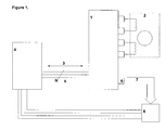
- Figure 1 shows an integrated circuit IC in the form of a motor driver circuit 1 having circuitry for driving the current in the windings of a motor 2.
- the motor driver IC 1 may exchange data 3 with a motor control circuit in the form of another integrated circuit 4, such as a micro-controller, through a data bus 5 linking the circuits 1 and 4.
- the circuit 1 makes a measurement from the drive circuitry for use as feedback in a control loop.
- the feedback may be in the form of a BEMF.
- the measurement of BEMF can be made in any way as is known from the art, and so need not be explained in more detail here. For example it can involve measuring voltage across the windings and voltage applied, or current through the windings.
- the BEMF information so gathered may be signal processed (for example filtered, amplified, sampled, ...) and is made available on a dedicated output 6 of the circuit 1.
- the signal processing might be needed to adjust the signal voltage amplitude to the required voltage ranges of the output contact and can consist of (but not limited to) for example voltage scaling through an analogue resistive divider or amplification or offset compensation through an amplification circuit or sampling as depicted in Figure 2 .
- the processed BEMF related data 7 on the output contact for example an output pin 6 is then directly available to an external circuit without having to go through the data bus 5. This means it is no longer necessary to format the BEMF related data 7 to fit the communication protocol used to exchange information between circuits 1 and 4 through the data bus 5.
- the data 7 is analog in nature it might for instance be sent to an analog to digital converter (ADC) 8 with the desired resolution (contrarily to what happens in the known art) to satisfy the requirements of a given motor drive application.
- ADC analog to digital converter
- the analog to digital converter 8 may be a stand alone component or may be part of the circuit 4.
- the bandwidth of the control loop will depend on the processing power of the circuit 4 and the data conversion rate of the analog to digital converter 8. Therefore a control loop of any desired bandwidth and precision can be realized by selecting the (most) suitable micro-controller and analog digital converter (both of which exist in a multitude of variations).
- there is no analog to digital converter 8 and the circuit 4 can be a continuous time analog regulator or filter that generates control signals transmitted on the bus 5 directly from the analog signal available on pin 6.
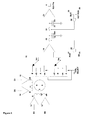
- FIG. 2 shows how the BEMF related information can be generated and shared on the output 6.
- motor 2 being a bipolar stepper motor without intent to restrict the invention to that particular case.
- the windings 10 and 11 of the bipolar stepper motor are alternatively driven by drivers 12, 13, 14 and 15 (controlled by circuitry not shown through the signals D0 to D3).
- the drivers 12, 13, 14 and 15 are integrated in the circuit 1.
- the drivers can be transistors associated to form an H-bridge, or other motor drive configurations can be used. In one example, the transistors are MOS transistors in a full H-bridge. During rotation of the rotor 9, the windings are driven for a proportion of each rotation.
- the permanent magnet(s) located at the rotor induces a BEMF in the windings 10 and 11 at the stator.
- the BEMF across the winding 10 or 11 can be measured when it is not energized (that is when the drivers do not force a current through the winding or do not impose a given voltage difference across the winding).
- the correct winding is selected at different parts of each rotation by a first selection circuit in the form of switches 16 controlled by winding select signals 17 (the signals 17 may be generated in a number of ways known to the art by circuitry not shown on figure 2 ).
- the BEMF across a given winding may be amplified and/or filtered by an amplifier and/or filter 18. The result is sampled and held under control of circuitry such as switches 20, 22 and the sampling capacitors 19 and 21.
- the voltage stored across capacitor 21 may be buffered by a buffer circuit 23 before being applied to the output pin 6.
- the switches 20 and 22 are open or closed as a function of signals generated by logic combinations of the binary signals 26 (SH - as sample and hold signal) 27 (POS - a signal related to the position of the rotor), 28 (NOT POS being the logical inverse of POS) and 29 (SLAT) as will be discussed below.
- the signal that closes or open the switch 20 is generated by AND-ing signals 26 and 27 with the AND gate 25.
- the signal that closes or open the switch 22 is generated by OR-ing signals 28 and 29 with the OR gate 25.
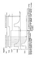
- the resulting signal available at the output pin 6 can be seen in the graph of figure 3 .
- time is represented left to right.
- a top line shows a timing of signal SH, which triggers the sample hold circuit..
- a second line shows binary signal POS.
- a third line shows SLAT.
- the SLAT signal 29 enables the user to chose between having the samples of the BEMF signal (Vbemf on figure 3 ) successively available on output pin 6 or having a chosen sample being held on output pin 6.
- the binary SLAT signal may be generated by any appropriate means (for example a mechanical switch such as a dipswitch connected to circuit 1, circuit 1 itself, control signals generated by circuit 4 and sent to circuit 1 through the communication bus 5, .
- a fourth line in fig 3 shows a bemf voltage signal, and the bottom line shows signal SLA, the analog output.
- the SLA output is "transparent", and at the right hand side in this example the output is only updated at the end of the period.
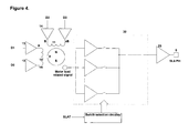
- Figure 4 shows another embodiment.
- the analog processing circuitry 30 has a number of distinct signal processing circuits for processing a motor load related signal. These can process the signal in different ways.
- the different outputs can be selected by switching or mixing, by selection circuitry.
- the selection circuitry can be driven by selection signal SLAT. The selected output is fed to the output contact 6. It can be combined with the selection circuit 16 for selecting different measurements for signal processing as shown in fig 2 .
- an output can be dedicated to an analog signal related to the back electromotive force whereas the prior art involves (a) the back electromotive force signal first being AD converted before being output over a general purpose communication port or (b) the back electromotive force signal being compared to a threshold value to generate a binary signal (Yes/No signal) made available on a dedicated output contact.
- a dedicated contact is a shared contact, for example sharing by time sharing, or by frequency sharing for example.
Landscapes
- Engineering & Computer Science (AREA)
- Power Engineering (AREA)
- Control Of Electric Motors In General (AREA)
- Control Of Stepping Motors (AREA)
- Control Of Ac Motors In General (AREA)
- Control Of Motors That Do Not Use Commutators (AREA)
- Control Of Direct Current Motors (AREA)
Abstract
Description
- The invention is related to integrated circuits for motor drivers that can make measurements for feedback purposes such as measurement of the back electromotive to drive electrical motors.
- The art recognizes the interest of integrated electrical motor driver circuit integrating as many functions as possible on the same semiconductor circuit and that are flexible enough to be used for various applications. For example, the same integrated motor driver circuit may be used to control a motor with or without sensor(s). The usual sensors known to the art for control of motors are hall sensors or optical encoders. Flexibility may also concern the format of the data and the amount of data that is made available to circuit(s) and/or components external to the integrated motor driver circuit: such data can be analog or digital in nature and if digital in nature, the number of bits used to encode the data might need to vary from one application to another in function of desired characteristics for the resulting motor drive / control loop.
- The art does recognize the advantage that there is to use the back electromotive force (BEMF) measured across the windings at the stator of a motor to derive signals that can be used to detect a stall condition, detect the position and/or speed of the rotor of a motor, determine the load conditions of a motor.... In particular as disclosed in the published patent application
EP-A-1460757 , it may be advantageous in certain applications to measure and use the BEMF at several sampling instants instead of a single BEMF measurement. - In the application note AN235/0788 Stepper Motor Driving by H. Sax from SGS-Thomson Microelectronics (a.k.a. ST), the art also recognizes the interest there is to reduce the number of connections between a first integrated circuit (a motor driver circuit) and a second integrated circuit (a control circuit or data processing circuit, digital or otherwise, in particular a micro-controller or micro-computer chip).
- TRINAMIC Motion control GmbH & Co KG offers a solution in the integrated circuit TMC 249/A. As described in the data sheet of the TMC 249/A (version 2.02 dated August 12th, 2005), the BEMF of a motor is measured in order to detect a stall condition of that motor. The BEMF measurement is made available as a digital, three bits indicator that can be shared with an external micro-controller through a serial interface.
- Freescale Semiconductor offers yet another solution in the integrated circuit MM908E625. This integrated circuit consists of basically 2 dies in one package: an analogue chip and a digital (microcontroller) chip. As described in the data sheet of the MM908E625 (Rev. 4.0 dated September 2005), the BEMF of a motor is measured indirectly by means of detecting the existence and duration of a recirculation current. A signal called "BEMF output" is basically a single bit flag (binary output data from an analogue comparator that is integrated in the analogue die) that indicates if (yes or no) a recirculation current in the motor exists. This flag is generated each PWM cycle during the recirculation phase and is made available as an analogue output for connection to the second die (the embedded microcontroller) for further processing inside the integrated circuit MM908E625. Because the information of the "BEMF output" is contained in the time-domain (i.e. the duration of the pulse "BEMF output" indicates the duration of the existence of recirculation current and this is a measure for the amount of Bemf), the microcontroller needs to be equipped with a timer circuit that measures the duration of the pulse. This timing information can then be transformed into other data and can be exchanged with an external circuit, in particular an external micro-controller, through a serial interface using output pins distinct from the BEMF pin.
- In yet other integrated circuits, those from the ST7MC family offered by ST, information related to the BEMF is offered under the form of a single bit binary signal on a first output pin of the semiconductor chip for use by external circuitry. The actual BEMF signal is available to a micro-controller integrated in the same semiconductor substrate as the motor driver circuit, thereby eliminating the need for transmission of detailed BEMF information to an external circuit.
- There remains a need to improve on the art.
- An object of the invention is to provide an improved apparatus or method. Some of the embodiments of the invention can provide a more flexible integrated electrical motor driver that can interface with as many different micro-controllers as possible, that can be used in both analog and discrete time feedback loop for motor control and that can satisfy various precision requirements (bit resolution and/or power dissipation, component counts, ...).
- According to a first aspect of the invention, there is provided an integrated circuit having drive circuitry to drive windings of an electrical motor, the integrated circuit comprising means to make a measurement from the drive circuitry during rotation of the motor suitable for use as motor control feedback. The integrated circuit has an output contact where the motor control feedback measurement is available as an analog output signal.
- An analog signal can assume a continuum of values (voltage or current) between a lower value and a higher value (e.g. between the ground reference and a supply voltage). A digital signal on the contrary is either low or high and e.g. 10 bits are necessary to encode an analog signal varying between 0 and 5V with a resolution of approximately 5mV. Those 10 bits must either be transmitted in parallel (at the cost of more pins and more connections) or in series (at the cost of bandwidth). This unusual approach is contrary to the usual trend of more and more digital processing. It was realized, after extensive experimentation with various communication protocols, and data formats that having the motor load related information obtained by the motor driver circuit available as an analog signal on a dedicated pin of said circuit gave the highest flexibility to the circuit. In other words, it allowed the design of motor control loop (1) with any bit resolution, (2) with a bandwidth limited to the processing speed of the micro-controller (if any) used, (3) that is either discrete time or continuous time.
- The analog feedback output gives more flexibility to the design of a motor control loop in terms of bit resolution, bandwidth and choice of discrete time or continuous time control.
- The analog signal available on the output pin may be the result of signal processing by one or more analog and/or digital circuits (integrated in the same semiconductor substrate as the motor driver) of motor load related information. These signal processing circuits may process the signal in series or in parallel. A binary signal may determine which output of said signal processing circuits will be made available on the output pin. In particular, the signal processing circuit may be a sample and hold circuit. Often, the motor load related signal is the back electromotive force (BEMF) that is induced in the windings of the motor during operation of said motor, though other signals are conceivable.
- Another aspect of the invention provides a system having the integrated circuit, and a motor control circuit coupled to receive the analog output signal.
- The integrated circuit according to embodiments of the present invention may be used with an external motor control circuit coupled to receive the analog output signal to generate motor control signals, to control the drive circuitry.
- According to embodiments of the present invention, the system comprises an integrated circuit according to the present invention, and a motor control circuit coupled to receive the analog output signal having the motor feedback measurement signal, from the integrated circuit. The motor control circuit may be arranged to use the motor control feedback signal to generate motor control signals, the motor control signals being coupled to the integrated circuit, to control the drive circuitry.
- According to some embodiments, the motor control circuit may comprise digital circuitry, and the system having a converter for converting the analog output signal to a digital signal.
- Any additional features can be added without departing from the scope of the claims. Any of the additional features can be combined together and combined with any of the aspects. Other advantages will be apparent to those skilled in the art, especially over other prior art. Numerous variations and modifications can be made without departing from the claims of the present invention. Therefore, it should be clearly understood that the form of the present invention is illustrative only and is not intended to limit the scope of the present invention.
- How the present invention may be put into effect will now be described by way of example with reference to the appended drawings, in which:
-
Figure 1 - Shows an integrated motor driver circuit according to embodiments of the present invention -
Figure 2 - Shows an example of measurement means used to generate the signal available on an output pin of the integrated motor driver circuit. -
Figure 3 - Shows signals generated during operation of the integrated motor driver circuit at a number of nodes of the circuit. -
Figure 4 - Shows a generalization of the circuit example circuit offigure 3 to any signals that are a function of motor load and/or speed. - The present invention will be described with respect to particular embodiments and with reference to certain drawings but the invention is not limited thereto but only by the claims. The drawings described are only schematic and are non-limiting. In the drawings, the size of some of the elements may be exaggerated and not drawn on scale for illustrative purposes. The dimensions and the relative dimensions do not correspond to actual reductions to practice of the invention.
- It is to be noticed that the term "comprising", used in the claims, should not be interpreted as being restricted to the means/steps listed thereafter; it does not exclude other elements or steps. It is thus to be interpreted as specifying the presence of the stated features, integers, steps or components as referred to, but does not preclude the presence or addition of one or more other features, integers, steps or components, or groups thereof. Thus, the scope of the expression "a device comprising means A and B" should not be limited to devices consisting only of components A and B. It means that with respect to the present invention, the only relevant components of the device are A and B.
- The invention will now be described by a detailed description of several embodiments of the invention. It is clear that other embodiments of the invention can be configured according to the knowledge of persons skilled in the art without departing from the true spirit or technical teaching of the invention, the invention being limited only by the terms of the appended claims.
- References to an integrated circuit can encompass a semiconductor die, in which case the output contact is typically a contact pad on the die. References to an integrated circuit can also encompass a packaged die, in which case the output contact is typically a pin, or pad, or solder ball, or similar, typically coupled to the die by a wire bond. The packaging of the die can encompass any type of packaging, including resin packaging, packaging as part of a hybrid circuit having die and other components, integrated or discrete, and so on. Hence references to an output contact can encompass a contact pad on the die, a wire bond, a contact on an integrated circuit package such as a pin, solder pad, or solder ball for example.
- Embodiments of the invention described below show examples of an integrated circuit having drive circuitry to drive the windings of an electrical motor, with means to make a measurement from the drive circuitry during rotation of the motor suitable for use as motor control feedback, as set out above.
- Additional features of some embodiments can include the measurement comprising a motor load related, or motor speed related measurement, or the measurement means being arranged to make a number of measurements and having a first selection circuit for selecting which of the measurements is to be output.
- Another such additional feature is one or more analog circuits for signal processing the motor control feedback measurement before it is output as the analog output signal. Another such additional feature is having a number of the analog circuits and having a second selection circuit for selecting which of the analog circuits is to be coupled to the output contact. At least one of the analog circuits can be a sample and hold circuit.
- The motor control feedback measurement can comprise a measurement of the back electromotive force (BEMF) generated across the windings of the motor during rotation of the rotor of said motor.
- It has now been appreciated that the prior art circuits suffer from several disadvantages: use of a specific communication interface (given protocol, number of bits, bit rate, ...) that may impose limits on the bandwidth of the control loop, use of a predetermined number of bits to encode BEMF related information that impose limitations on the precision that can be achieved for the resulting motor drive, use of a given/specific micro-controller when it is in the same chip (same package or same semiconductor substrate) as the motor drive circuitry.
- It has now been appreciated that there can be benefit from an integrated motor driver circuit that would reduce the number of connections between an integrated motor driver circuit and a micro-controller yet be flexible enough to satisfy the needs of motor control applications regardless of the nature of the signals (analog or digital, in particular motor load or BEMF related signals and in general signals that are function of the motor load), the number of bits used to encode signals (in particular motor load or BEMF related signals), the required bandwidth expected from the motor drive, and so on.
-
Figure 1 shows an integrated circuit IC in the form of amotor driver circuit 1 having circuitry for driving the current in the windings of amotor 2. Themotor driver IC 1 may exchangedata 3 with a motor control circuit in the form of anotherintegrated circuit 4, such as a micro-controller, through adata bus 5 linking thecircuits circuit 1 makes a measurement from the drive circuitry for use as feedback in a control loop. The feedback may be in the form of a BEMF. The measurement of BEMF can be made in any way as is known from the art, and so need not be explained in more detail here. For example it can involve measuring voltage across the windings and voltage applied, or current through the windings. The BEMF information so gathered may be signal processed (for example filtered, amplified, sampled, ...) and is made available on adedicated output 6 of thecircuit 1. The signal processing might be needed to adjust the signal voltage amplitude to the required voltage ranges of the output contact and can consist of (but not limited to) for example voltage scaling through an analogue resistive divider or amplification or offset compensation through an amplification circuit or sampling as depicted inFigure 2 . The processed BEMFrelated data 7 on the output contact, for example anoutput pin 6 is then directly available to an external circuit without having to go through thedata bus 5. This means it is no longer necessary to format the BEMFrelated data 7 to fit the communication protocol used to exchange information betweencircuits data bus 5. If thedata 7 is analog in nature it might for instance be sent to an analog to digital converter (ADC) 8 with the desired resolution (contrarily to what happens in the known art) to satisfy the requirements of a given motor drive application. The analog todigital converter 8 may be a stand alone component or may be part of thecircuit 4. The bandwidth of the control loop will depend on the processing power of thecircuit 4 and the data conversion rate of the analog todigital converter 8. Therefore a control loop of any desired bandwidth and precision can be realized by selecting the (most) suitable micro-controller and analog digital converter (both of which exist in a multitude of variations). In some embodiments, there is no analog todigital converter 8 and thecircuit 4 can be a continuous time analog regulator or filter that generates control signals transmitted on thebus 5 directly from the analog signal available onpin 6. -
Figure 2 shows how the BEMF related information can be generated and shared on theoutput 6. For the sake of clarity we will discuss the particular case ofmotor 2 being a bipolar stepper motor without intent to restrict the invention to that particular case. Thewindings drivers drivers circuit 1. The drivers can be transistors associated to form an H-bridge, or other motor drive configurations can be used. In one example, the transistors are MOS transistors in a full H-bridge. During rotation of therotor 9, the windings are driven for a proportion of each rotation. The permanent magnet(s) located at the rotor induces a BEMF in thewindings switches 16 controlled by winding select signals 17 (thesignals 17 may be generated in a number of ways known to the art by circuitry not shown onfigure 2 ). - The BEMF across a given winding may be amplified and/or filtered by an amplifier and/or
filter 18. The result is sampled and held under control of circuitry such asswitches sampling capacitors capacitor 21 may be buffered by abuffer circuit 23 before being applied to theoutput pin 6. - The
switches switch 20 is generated by AND-ing signals 26 and 27 with the ANDgate 25. The signal that closes or open theswitch 22 is generated by OR-ing signals OR gate 25. - The resulting signal available at the
output pin 6 can be seen in the graph offigure 3 . Infig 3 , time is represented left to right. A top line shows a timing of signal SH, which triggers the sample hold circuit.. A second line shows binary signal POS. A third line shows SLAT. TheSLAT signal 29 enables the user to chose between having the samples of the BEMF signal (Vbemf onfigure 3 ) successively available onoutput pin 6 or having a chosen sample being held onoutput pin 6. The binary SLAT signal may be generated by any appropriate means (for example a mechanical switch such as a dipswitch connected tocircuit 1,circuit 1 itself, control signals generated bycircuit 4 and sent tocircuit 1 through thecommunication bus 5, ...). - A fourth line in
fig 3 shows a bemf voltage signal, and the bottom line shows signal SLA, the analog output. At the left hand side, the SLA output is "transparent", and at the right hand side in this example the output is only updated at the end of the period. -
Figure 4 shows another embodiment. In this case theanalog processing circuitry 30 has a number of distinct signal processing circuits for processing a motor load related signal. These can process the signal in different ways. The different outputs can be selected by switching or mixing, by selection circuitry. The selection circuitry can be driven by selection signal SLAT. The selected output is fed to theoutput contact 6. It can be combined with theselection circuit 16 for selecting different measurements for signal processing as shown infig 2 . - As has been described, an output can be dedicated to an analog signal related to the back electromotive force whereas the prior art involves (a) the back electromotive force signal first being AD converted before being output over a general purpose communication port or (b) the back electromotive force signal being compared to a threshold value to generate a binary signal (Yes/No signal) made available on a dedicated output contact. Another alternative to a dedicated contact is a shared contact, for example sharing by time sharing, or by frequency sharing for example. Although the examples described show only a single output, clearly it is feasible to have two or more contacts for separate feedback signals, according to the application.
Claims (9)
- An integrated circuit (1) having drive circuitry (12,13,14,15) to drive the windings of an electrical motor (2), the integrated circuit (1) comprising means to make a measurement from the drive circuitry during rotation of the motor (2), suitable for use as motor control feedback, the integrated circuit (1) being characterized by an output contact (6) through which the motor control feedback measurement is available as an analog output signal.
- The integrated circuit of claim 1, wherein the measurement comprises a motor load related, or motor speed related measurement.
- The integrated circuit of claim 1 or 2, wherein the measurement means is arranged to make a number of measurements and having a first selection circuit (17) for selecting which of the measurements is to be output.
- The integrated circuit of claim 1 having one or more analog circuits (18, 19, 20, 21, 22, 23) for signal processing the motor control feedback measurement before it is output as the analog output signal.
- The integrated circuit of claim 4 having a number of the analog circuits and having a second selection circuit for selecting which of the analog circuits (10) is to be coupled to the output contact (6).
- The integrated circuit of claim 4 or 5 where at least one of the analog circuits is a sample and hold circuit.
- The integrated circuit of any preceding claim where the motor control feedback measurement comprises a measurement of the back electromotive force (BEMF) generated across the windings of the motor (2) during rotation of the rotor of said motor (2).
- A system having an integrated circuit of any preceding claim, and a motor control circuit (4) coupled to receive the analog output signal having the motor feedback measurement signal, from the integrated circuit, the motor control circuit being arranged to use the motor control feedback signal to generate motor control signals, the motor control signals being coupled to the integrated circuit, to control the drive circuitry.
- The system of claim 8, the motor control circuit comprising digital circuitry, and the system having a converter for converting the analog output signal to a digital signal.
Applications Claiming Priority (1)
| Application Number | Priority Date | Filing Date | Title |
|---|---|---|---|
| GBGB0704439.9A GB0704439D0 (en) | 2007-03-08 | 2007-03-08 | Output contact for feedback in intergrated circuit motor driver |
Publications (2)
| Publication Number | Publication Date |
|---|---|
| EP1968183A1 true EP1968183A1 (en) | 2008-09-10 |
| EP1968183B1 EP1968183B1 (en) | 2011-03-23 |
Family
ID=37988567
Family Applications (1)
| Application Number | Title | Priority Date | Filing Date |
|---|---|---|---|
| EP08075141A Not-in-force EP1968183B1 (en) | 2007-03-08 | 2008-02-25 | Output contact for feedback in integrated circuit motor driver |
Country Status (8)
| Country | Link |
|---|---|
| US (1) | US8339092B2 (en) |
| EP (1) | EP1968183B1 (en) |
| JP (1) | JP5775247B2 (en) |
| CN (1) | CN101261311B (en) |
| AT (1) | ATE503297T1 (en) |
| DE (1) | DE602008005658D1 (en) |
| GB (1) | GB0704439D0 (en) |
| TW (1) | TWI436579B (en) |
Cited By (2)
| Publication number | Priority date | Publication date | Assignee | Title |
|---|---|---|---|---|
| US8058894B2 (en) | 2009-03-31 | 2011-11-15 | Semiconductor Components Industries, Llc | Method for detecting a fault condition |
| US8736298B2 (en) | 2011-10-26 | 2014-05-27 | Semiconductor Components Industries, Llc | Method for detecting a step loss condition |
Families Citing this family (5)
| Publication number | Priority date | Publication date | Assignee | Title |
|---|---|---|---|---|
| WO2007131947A1 (en) * | 2006-05-17 | 2007-11-22 | Continental Teves Ag & Co. Ohg | Method and pulse-width-modulated current control circuit for driving inductive loads in motor vehicles |
| US8089239B2 (en) * | 2008-04-16 | 2012-01-03 | Renesas Electronics America Inc. | Advanced method for stepper motor speed determination |
| GB2462948B (en) * | 2009-10-15 | 2011-08-31 | Protean Holdings Corp | Method and system for measuring a characteristic of an electric motor |
| CN106685285A (en) * | 2016-12-29 | 2017-05-17 | 深圳市微芯智能科技有限公司 | Integrated chip for driving stepping motor and motor driving device |
| US11447108B1 (en) * | 2017-10-30 | 2022-09-20 | Creed Monarch, Inc. | Braking control system and method to sysnchronize the operation of the braking of a towed vehicle |
Citations (6)
| Publication number | Priority date | Publication date | Assignee | Title |
|---|---|---|---|---|
| JP2002236136A (en) * | 2001-02-08 | 2002-08-23 | Shindengen Electric Mfg Co Ltd | Measuring device |
| US6504328B1 (en) * | 1995-02-24 | 2003-01-07 | Stmicroelectronics Inc. | Sensorless motor driver with BEMF mask extender |
| EP1303036A2 (en) * | 2001-10-16 | 2003-04-16 | STMicroelectronics, Inc. | Multi-mode motor controller chip set |
| EP1460757A1 (en) | 2003-03-21 | 2004-09-22 | AMI Semiconductor Belgium BVBA | Device and method for detecting rotor speed of a multiple phase motor with bipolar drive |
| US20050184688A1 (en) * | 2004-02-24 | 2005-08-25 | Denso Corporation | Brushless motor driving device |
| US20050248305A1 (en) * | 2004-05-04 | 2005-11-10 | International Business Machines Corporation | Method, system, and program product for feedback control of a target system utilizing imposition of a periodic modulating signal onto a command signal |
Family Cites Families (27)
| Publication number | Priority date | Publication date | Assignee | Title |
|---|---|---|---|---|
| DE3140432C2 (en) * | 1980-10-13 | 1985-10-10 | Hitachi, Ltd., Tokio/Tokyo | Speed control circuit |
| US4737661A (en) * | 1985-08-09 | 1988-04-12 | Black & Decker Inc. | Variable speed trigger switch |
| US4679102A (en) * | 1985-11-20 | 1987-07-07 | Seagate Technology | Method and means for parking read/write heads in a disc drive using the back-EMF of the spindle motor to operate a stepper motor |
| US4978909A (en) * | 1988-11-14 | 1990-12-18 | Martin Marietta Energy Systems, Inc. | Demodulation circuit for AC motor current spectral analysis |
| US5182685A (en) * | 1989-02-03 | 1993-01-26 | Seagate Technology, Inc. | Stepper motor torque variance compensation using varied applied voltage |
| US5017845A (en) * | 1990-10-05 | 1991-05-21 | Sgs-Thomson Microelectronics, Inc. | Brushless direct current motor starting and operating apparatus and method |
| JPH05207799A (en) * | 1991-11-04 | 1993-08-13 | Xerox Corp | Control system of stepping motor |
| US5592058A (en) * | 1992-05-27 | 1997-01-07 | General Electric Company | Control system and methods for a multiparameter electronically commutated motor |
| US5444583A (en) * | 1992-09-30 | 1995-08-22 | Quantum Corporation | Disk drive having on-board triggered digital sampling analyzer |
| WO1994026022A1 (en) * | 1993-04-27 | 1994-11-10 | Sankyo Seiki Mfg. Co., Ltd. | Device for detecting rotational position of brushless motor |
| US5586306A (en) * | 1993-06-04 | 1996-12-17 | Cirrus Logic, Inc. | Integrated circuit servo system control for computer mass storage device with distributed control functionality to reduce transport delay |
| KR950004717A (en) * | 1993-07-15 | 1995-02-18 | 가나이 쯔또무 | Brushless Motor Drive Circuit |
| US5530326A (en) * | 1993-07-19 | 1996-06-25 | Quantum Corporation | Brushless DC spindle motor startup control |
| US5584524A (en) * | 1994-12-01 | 1996-12-17 | Vogel; Tony | Liner for truck bed |
| DE19511865C1 (en) * | 1995-03-31 | 1996-06-05 | Daimler Benz Ag | Setting element drive using electric stepping motor |
| JP3958819B2 (en) * | 1997-01-31 | 2007-08-15 | ミネベア株式会社 | Method of driving a two-phase claw pole type stepping motor used in a recording disk driving device of an information storage device |
| US6081091A (en) * | 1999-03-08 | 2000-06-27 | Motorola, Inc. | Motor controller, integrated circuit, and method of controlling a motor |
| US6686761B2 (en) * | 2000-06-27 | 2004-02-03 | Industrial Technology Research Institute | Method for determining whether a rotor is good in magnetic induction by measuring the EMF of a motor |
| JP3353781B2 (en) * | 2000-09-28 | 2002-12-03 | 松下電器産業株式会社 | Motor control device |
| CA2513550A1 (en) * | 2003-01-24 | 2004-08-12 | Tecumseh Products Company | Brushless and sensorless dc motor control system with locked and stopped rotor detection |
| JP3813587B2 (en) * | 2003-01-30 | 2006-08-23 | 東芝エルエスアイシステムサポート株式会社 | Motor control circuit, semiconductor integrated circuit, pointing device, and motor control method |
| JP4420317B2 (en) * | 2003-09-26 | 2010-02-24 | 株式会社ルネサステクノロジ | Motor driving device and integrated circuit device for motor driving |
| KR100532483B1 (en) * | 2003-12-12 | 2005-12-02 | 삼성전자주식회사 | Calibration method and apparatus therefor |
| JP2005228733A (en) * | 2004-01-16 | 2005-08-25 | Fuji Photo Film Co Ltd | Light-emitting element |
| JP4565466B2 (en) * | 2004-02-26 | 2010-10-20 | ルネサスエレクトロニクス株式会社 | Motor driving device and integrated circuit device for motor driving |
| JP4583111B2 (en) * | 2004-08-31 | 2010-11-17 | ルネサスエレクトロニクス株式会社 | Motor drive control device and disk rotation system |
| JP4877764B2 (en) * | 2006-08-01 | 2012-02-15 | ローム株式会社 | Motor drive circuit, method and disk device using them |
-
2007
- 2007-03-08 GB GBGB0704439.9A patent/GB0704439D0/en not_active Ceased
-
2008
- 2008-02-20 TW TW097105848A patent/TWI436579B/en active
- 2008-02-25 DE DE602008005658T patent/DE602008005658D1/en active Active
- 2008-02-25 AT AT08075141T patent/ATE503297T1/en not_active IP Right Cessation
- 2008-02-25 EP EP08075141A patent/EP1968183B1/en not_active Not-in-force
- 2008-03-05 JP JP2008054788A patent/JP5775247B2/en active Active
- 2008-03-05 US US12/042,724 patent/US8339092B2/en active Active
- 2008-03-07 CN CN2008100817445A patent/CN101261311B/en not_active Expired - Fee Related
Patent Citations (6)
| Publication number | Priority date | Publication date | Assignee | Title |
|---|---|---|---|---|
| US6504328B1 (en) * | 1995-02-24 | 2003-01-07 | Stmicroelectronics Inc. | Sensorless motor driver with BEMF mask extender |
| JP2002236136A (en) * | 2001-02-08 | 2002-08-23 | Shindengen Electric Mfg Co Ltd | Measuring device |
| EP1303036A2 (en) * | 2001-10-16 | 2003-04-16 | STMicroelectronics, Inc. | Multi-mode motor controller chip set |
| EP1460757A1 (en) | 2003-03-21 | 2004-09-22 | AMI Semiconductor Belgium BVBA | Device and method for detecting rotor speed of a multiple phase motor with bipolar drive |
| US20050184688A1 (en) * | 2004-02-24 | 2005-08-25 | Denso Corporation | Brushless motor driving device |
| US20050248305A1 (en) * | 2004-05-04 | 2005-11-10 | International Business Machines Corporation | Method, system, and program product for feedback control of a target system utilizing imposition of a periodic modulating signal onto a command signal |
Cited By (2)
| Publication number | Priority date | Publication date | Assignee | Title |
|---|---|---|---|---|
| US8058894B2 (en) | 2009-03-31 | 2011-11-15 | Semiconductor Components Industries, Llc | Method for detecting a fault condition |
| US8736298B2 (en) | 2011-10-26 | 2014-05-27 | Semiconductor Components Industries, Llc | Method for detecting a step loss condition |
Also Published As
| Publication number | Publication date |
|---|---|
| JP5775247B2 (en) | 2015-09-09 |
| TW200849796A (en) | 2008-12-16 |
| CN101261311A (en) | 2008-09-10 |
| ATE503297T1 (en) | 2011-04-15 |
| DE602008005658D1 (en) | 2011-05-05 |
| CN101261311B (en) | 2013-03-13 |
| US20080218113A1 (en) | 2008-09-11 |
| JP2008228561A (en) | 2008-09-25 |
| EP1968183B1 (en) | 2011-03-23 |
| US8339092B2 (en) | 2012-12-25 |
| TWI436579B (en) | 2014-05-01 |
| GB0704439D0 (en) | 2007-04-18 |
Similar Documents
| Publication | Publication Date | Title |
|---|---|---|
| EP1968183B1 (en) | Output contact for feedback in integrated circuit motor driver | |
| CN1238960C (en) | Frequency converter device | |
| TW533673B (en) | Sensorless control device for synchronous electric motor | |
| EP1460757A1 (en) | Device and method for detecting rotor speed of a multiple phase motor with bipolar drive | |
| CN101232266A (en) | Control method and device of DC brushless motor | |
| US10199974B2 (en) | Motor driving circuit and motor driving method | |
| TW201126889A (en) | Driving circuit | |
| KR20150071449A (en) | Apparatus for driving motor and Controlling Method thereof | |
| EP2345148B1 (en) | Method of detecting an operating condition of an electric stepper motor | |
| KR101203088B1 (en) | Stationary position detection apparatus | |
| US10910967B2 (en) | Motor driver device and semiconductor device | |
| CN209963970U (en) | Half-bridge drive circuit and related system | |
| US9300238B2 (en) | Motor driving device | |
| KR20200023224A (en) | Hall element sensing circuit | |
| JP2020025435A (en) | Integrated circuit and motor device | |
| US20250007433A1 (en) | Method and driver circuit for sensorless stepper motor back electromotive force detection | |
| CN115811261B (en) | Motor multi-turn counting device, method, drive system, and joint control system | |
| CN107703929B (en) | DC brushless motor controller testing device | |
| TW201705671A (en) | Control apparatus for dynamically adjusting a phase switching of the DC motor and method thereof | |
| US9257919B2 (en) | Method and apparatus for brushless DC motor control | |
| KR100492616B1 (en) | Device of pulse translation for frequency generator of bldc motor | |
| JP2008193777A (en) | Control method and controller of dc brushless motor | |
| JP4409663B2 (en) | Motor rotation pulse output circuit | |
| Morar | Unipolar Fixed-current Chopper–4 Phase Stepper Motor Driver System | |
| JP3075647U (en) | Hall element sensitive three-phase DC brushless motor |
Legal Events
| Date | Code | Title | Description |
|---|---|---|---|
| PUAI | Public reference made under article 153(3) epc to a published international application that has entered the european phase |
Free format text: ORIGINAL CODE: 0009012 |
|
| AK | Designated contracting states |
Kind code of ref document: A1 Designated state(s): AT BE BG CH CY CZ DE DK EE ES FI FR GB GR HR HU IE IS IT LI LT LU LV MC MT NL NO PL PT RO SE SI SK TR |
|
| AX | Request for extension of the european patent |
Extension state: AL BA MK RS |
|
| 17P | Request for examination filed |
Effective date: 20090305 |
|
| AKX | Designation fees paid |
Designated state(s): AT BE BG CH CY CZ DE DK EE ES FI FR GB GR HR HU IE IS IT LI LT LU LV MC MT NL NO PL PT RO SE SI SK TR |
|
| 17Q | First examination report despatched |
Effective date: 20091103 |
|
| RAP1 | Party data changed (applicant data changed or rights of an application transferred) |
Owner name: SEMICONDUCTOR COMPONENTS INDUSTRIES, LLC |
|
| GRAP | Despatch of communication of intention to grant a patent |
Free format text: ORIGINAL CODE: EPIDOSNIGR1 |
|
| GRAS | Grant fee paid |
Free format text: ORIGINAL CODE: EPIDOSNIGR3 |
|
| GRAA | (expected) grant |
Free format text: ORIGINAL CODE: 0009210 |
|
| AK | Designated contracting states |
Kind code of ref document: B1 Designated state(s): AT BE BG CH CY CZ DE DK EE ES FI FR GB GR HR HU IE IS IT LI LT LU LV MC MT NL NO PL PT RO SE SI SK TR |
|
| REG | Reference to a national code |
Ref country code: GB Ref legal event code: FG4D |
|
| REG | Reference to a national code |
Ref country code: CH Ref legal event code: EP |
|
| REG | Reference to a national code |
Ref country code: IE Ref legal event code: FG4D |
|
| REF | Corresponds to: |
Ref document number: 602008005658 Country of ref document: DE Date of ref document: 20110505 Kind code of ref document: P |
|
| REG | Reference to a national code |
Ref country code: DE Ref legal event code: R096 Ref document number: 602008005658 Country of ref document: DE Effective date: 20110505 |
|
| REG | Reference to a national code |
Ref country code: NL Ref legal event code: VDEP Effective date: 20110323 |
|
| PG25 | Lapsed in a contracting state [announced via postgrant information from national office to epo] |
Ref country code: GR Free format text: LAPSE BECAUSE OF FAILURE TO SUBMIT A TRANSLATION OF THE DESCRIPTION OR TO PAY THE FEE WITHIN THE PRESCRIBED TIME-LIMIT Effective date: 20110624 Ref country code: LV Free format text: LAPSE BECAUSE OF FAILURE TO SUBMIT A TRANSLATION OF THE DESCRIPTION OR TO PAY THE FEE WITHIN THE PRESCRIBED TIME-LIMIT Effective date: 20110323 Ref country code: SE Free format text: LAPSE BECAUSE OF FAILURE TO SUBMIT A TRANSLATION OF THE DESCRIPTION OR TO PAY THE FEE WITHIN THE PRESCRIBED TIME-LIMIT Effective date: 20110323 Ref country code: HR Free format text: LAPSE BECAUSE OF FAILURE TO SUBMIT A TRANSLATION OF THE DESCRIPTION OR TO PAY THE FEE WITHIN THE PRESCRIBED TIME-LIMIT Effective date: 20110323 Ref country code: LT Free format text: LAPSE BECAUSE OF FAILURE TO SUBMIT A TRANSLATION OF THE DESCRIPTION OR TO PAY THE FEE WITHIN THE PRESCRIBED TIME-LIMIT Effective date: 20110323 |
|
| LTIE | Lt: invalidation of european patent or patent extension |
Effective date: 20110323 |
|
| PG25 | Lapsed in a contracting state [announced via postgrant information from national office to epo] |
Ref country code: SI Free format text: LAPSE BECAUSE OF FAILURE TO SUBMIT A TRANSLATION OF THE DESCRIPTION OR TO PAY THE FEE WITHIN THE PRESCRIBED TIME-LIMIT Effective date: 20110323 Ref country code: FI Free format text: LAPSE BECAUSE OF FAILURE TO SUBMIT A TRANSLATION OF THE DESCRIPTION OR TO PAY THE FEE WITHIN THE PRESCRIBED TIME-LIMIT Effective date: 20110323 Ref country code: AT Free format text: LAPSE BECAUSE OF FAILURE TO SUBMIT A TRANSLATION OF THE DESCRIPTION OR TO PAY THE FEE WITHIN THE PRESCRIBED TIME-LIMIT Effective date: 20110323 Ref country code: BG Free format text: LAPSE BECAUSE OF FAILURE TO SUBMIT A TRANSLATION OF THE DESCRIPTION OR TO PAY THE FEE WITHIN THE PRESCRIBED TIME-LIMIT Effective date: 20110623 Ref country code: NO Free format text: LAPSE BECAUSE OF FAILURE TO SUBMIT A TRANSLATION OF THE DESCRIPTION OR TO PAY THE FEE WITHIN THE PRESCRIBED TIME-LIMIT Effective date: 20110623 Ref country code: CY Free format text: LAPSE BECAUSE OF FAILURE TO SUBMIT A TRANSLATION OF THE DESCRIPTION OR TO PAY THE FEE WITHIN THE PRESCRIBED TIME-LIMIT Effective date: 20110323 |
|
| PG25 | Lapsed in a contracting state [announced via postgrant information from national office to epo] |
Ref country code: BE Free format text: LAPSE BECAUSE OF FAILURE TO SUBMIT A TRANSLATION OF THE DESCRIPTION OR TO PAY THE FEE WITHIN THE PRESCRIBED TIME-LIMIT Effective date: 20110323 |
|
| PG25 | Lapsed in a contracting state [announced via postgrant information from national office to epo] |
Ref country code: EE Free format text: LAPSE BECAUSE OF FAILURE TO SUBMIT A TRANSLATION OF THE DESCRIPTION OR TO PAY THE FEE WITHIN THE PRESCRIBED TIME-LIMIT Effective date: 20110323 Ref country code: PT Free format text: LAPSE BECAUSE OF FAILURE TO SUBMIT A TRANSLATION OF THE DESCRIPTION OR TO PAY THE FEE WITHIN THE PRESCRIBED TIME-LIMIT Effective date: 20110725 |
|
| PG25 | Lapsed in a contracting state [announced via postgrant information from national office to epo] |
Ref country code: IS Free format text: LAPSE BECAUSE OF FAILURE TO SUBMIT A TRANSLATION OF THE DESCRIPTION OR TO PAY THE FEE WITHIN THE PRESCRIBED TIME-LIMIT Effective date: 20110723 Ref country code: RO Free format text: LAPSE BECAUSE OF FAILURE TO SUBMIT A TRANSLATION OF THE DESCRIPTION OR TO PAY THE FEE WITHIN THE PRESCRIBED TIME-LIMIT Effective date: 20110323 Ref country code: SK Free format text: LAPSE BECAUSE OF FAILURE TO SUBMIT A TRANSLATION OF THE DESCRIPTION OR TO PAY THE FEE WITHIN THE PRESCRIBED TIME-LIMIT Effective date: 20110323 Ref country code: CZ Free format text: LAPSE BECAUSE OF FAILURE TO SUBMIT A TRANSLATION OF THE DESCRIPTION OR TO PAY THE FEE WITHIN THE PRESCRIBED TIME-LIMIT Effective date: 20110323 Ref country code: ES Free format text: LAPSE BECAUSE OF FAILURE TO SUBMIT A TRANSLATION OF THE DESCRIPTION OR TO PAY THE FEE WITHIN THE PRESCRIBED TIME-LIMIT Effective date: 20110704 |
|
| PG25 | Lapsed in a contracting state [announced via postgrant information from national office to epo] |
Ref country code: NL Free format text: LAPSE BECAUSE OF FAILURE TO SUBMIT A TRANSLATION OF THE DESCRIPTION OR TO PAY THE FEE WITHIN THE PRESCRIBED TIME-LIMIT Effective date: 20110323 |
|
| PLBE | No opposition filed within time limit |
Free format text: ORIGINAL CODE: 0009261 |
|
| STAA | Information on the status of an ep patent application or granted ep patent |
Free format text: STATUS: NO OPPOSITION FILED WITHIN TIME LIMIT |
|
| 26N | No opposition filed |
Effective date: 20111227 |
|
| PG25 | Lapsed in a contracting state [announced via postgrant information from national office to epo] |
Ref country code: DK Free format text: LAPSE BECAUSE OF FAILURE TO SUBMIT A TRANSLATION OF THE DESCRIPTION OR TO PAY THE FEE WITHIN THE PRESCRIBED TIME-LIMIT Effective date: 20110323 Ref country code: PL Free format text: LAPSE BECAUSE OF FAILURE TO SUBMIT A TRANSLATION OF THE DESCRIPTION OR TO PAY THE FEE WITHIN THE PRESCRIBED TIME-LIMIT Effective date: 20110323 |
|
| REG | Reference to a national code |
Ref country code: DE Ref legal event code: R097 Ref document number: 602008005658 Country of ref document: DE Effective date: 20111227 |
|
| PG25 | Lapsed in a contracting state [announced via postgrant information from national office to epo] |
Ref country code: IT Free format text: LAPSE BECAUSE OF FAILURE TO SUBMIT A TRANSLATION OF THE DESCRIPTION OR TO PAY THE FEE WITHIN THE PRESCRIBED TIME-LIMIT Effective date: 20110323 |
|
| PG25 | Lapsed in a contracting state [announced via postgrant information from national office to epo] |
Ref country code: MC Free format text: LAPSE BECAUSE OF NON-PAYMENT OF DUE FEES Effective date: 20120229 |
|
| REG | Reference to a national code |
Ref country code: CH Ref legal event code: PL |
|
| PG25 | Lapsed in a contracting state [announced via postgrant information from national office to epo] |
Ref country code: LI Free format text: LAPSE BECAUSE OF NON-PAYMENT OF DUE FEES Effective date: 20120229 Ref country code: CH Free format text: LAPSE BECAUSE OF NON-PAYMENT OF DUE FEES Effective date: 20120229 |
|
| REG | Reference to a national code |
Ref country code: IE Ref legal event code: MM4A |
|
| PG25 | Lapsed in a contracting state [announced via postgrant information from national office to epo] |
Ref country code: IE Free format text: LAPSE BECAUSE OF NON-PAYMENT OF DUE FEES Effective date: 20120225 |
|
| PG25 | Lapsed in a contracting state [announced via postgrant information from national office to epo] |
Ref country code: MT Free format text: LAPSE BECAUSE OF FAILURE TO SUBMIT A TRANSLATION OF THE DESCRIPTION OR TO PAY THE FEE WITHIN THE PRESCRIBED TIME-LIMIT Effective date: 20110323 |
|
| PG25 | Lapsed in a contracting state [announced via postgrant information from national office to epo] |
Ref country code: TR Free format text: LAPSE BECAUSE OF FAILURE TO SUBMIT A TRANSLATION OF THE DESCRIPTION OR TO PAY THE FEE WITHIN THE PRESCRIBED TIME-LIMIT Effective date: 20110323 |
|
| PG25 | Lapsed in a contracting state [announced via postgrant information from national office to epo] |
Ref country code: LU Free format text: LAPSE BECAUSE OF NON-PAYMENT OF DUE FEES Effective date: 20120225 |
|
| PG25 | Lapsed in a contracting state [announced via postgrant information from national office to epo] |
Ref country code: HU Free format text: LAPSE BECAUSE OF FAILURE TO SUBMIT A TRANSLATION OF THE DESCRIPTION OR TO PAY THE FEE WITHIN THE PRESCRIBED TIME-LIMIT Effective date: 20080225 |
|
| REG | Reference to a national code |
Ref country code: FR Ref legal event code: PLFP Year of fee payment: 9 |
|
| REG | Reference to a national code |
Ref country code: FR Ref legal event code: PLFP Year of fee payment: 10 |
|
| REG | Reference to a national code |
Ref country code: FR Ref legal event code: PLFP Year of fee payment: 11 |
|
| PGFP | Annual fee paid to national office [announced via postgrant information from national office to epo] |
Ref country code: DE Payment date: 20210120 Year of fee payment: 14 Ref country code: GB Payment date: 20210120 Year of fee payment: 14 |
|
| REG | Reference to a national code |
Ref country code: DE Ref legal event code: R119 Ref document number: 602008005658 Country of ref document: DE |
|
| GBPC | Gb: european patent ceased through non-payment of renewal fee |
Effective date: 20220225 |
|
| PG25 | Lapsed in a contracting state [announced via postgrant information from national office to epo] |
Ref country code: GB Free format text: LAPSE BECAUSE OF NON-PAYMENT OF DUE FEES Effective date: 20220225 Ref country code: DE Free format text: LAPSE BECAUSE OF NON-PAYMENT OF DUE FEES Effective date: 20220901 |
|
| P01 | Opt-out of the competence of the unified patent court (upc) registered |
Effective date: 20230519 |
|
| PGFP | Annual fee paid to national office [announced via postgrant information from national office to epo] |
Ref country code: FR Payment date: 20240123 Year of fee payment: 17 |
|
| PG25 | Lapsed in a contracting state [announced via postgrant information from national office to epo] |
Ref country code: FR Free format text: LAPSE BECAUSE OF NON-PAYMENT OF DUE FEES Effective date: 20250228 |