EP1968109A2 - Semiconductor device and method of manufacturing the same - Google Patents
Semiconductor device and method of manufacturing the same Download PDFInfo
- Publication number
- EP1968109A2 EP1968109A2 EP08004084A EP08004084A EP1968109A2 EP 1968109 A2 EP1968109 A2 EP 1968109A2 EP 08004084 A EP08004084 A EP 08004084A EP 08004084 A EP08004084 A EP 08004084A EP 1968109 A2 EP1968109 A2 EP 1968109A2
- Authority
- EP
- European Patent Office
- Prior art keywords
- region
- main face
- semiconductor device
- semiconductor chip
- crystalline defect
- Prior art date
- Legal status (The legal status is an assumption and is not a legal conclusion. Google has not performed a legal analysis and makes no representation as to the accuracy of the status listed.)
- Withdrawn
Links
Images





Classifications
-
- H—ELECTRICITY
- H10—SEMICONDUCTOR DEVICES; ELECTRIC SOLID-STATE DEVICES NOT OTHERWISE PROVIDED FOR
- H10W—GENERIC PACKAGES, INTERCONNECTIONS, CONNECTORS OR OTHER CONSTRUCTIONAL DETAILS OF DEVICES COVERED BY CLASS H10
- H10W70/00—Package substrates; Interposers; Redistribution layers [RDL]
- H10W70/60—Insulating or insulated package substrates; Interposers; Redistribution layers
- H10W70/67—Insulating or insulated package substrates; Interposers; Redistribution layers characterised by their insulating layers or insulating parts
- H10W70/68—Shapes or dispositions thereof
- H10W70/6875—Shapes or dispositions thereof being on a metallic substrate, e.g. insulated metal substrates [IMS]
-
- H—ELECTRICITY
- H10—SEMICONDUCTOR DEVICES; ELECTRIC SOLID-STATE DEVICES NOT OTHERWISE PROVIDED FOR
- H10D—INORGANIC ELECTRIC SEMICONDUCTOR DEVICES
- H10D62/00—Semiconductor bodies, or regions thereof, of devices having potential barriers
- H10D62/10—Shapes, relative sizes or dispositions of the regions of the semiconductor bodies; Shapes of the semiconductor bodies
- H10D62/117—Shapes of semiconductor bodies
-
- H—ELECTRICITY
- H10—SEMICONDUCTOR DEVICES; ELECTRIC SOLID-STATE DEVICES NOT OTHERWISE PROVIDED FOR
- H10D—INORGANIC ELECTRIC SEMICONDUCTOR DEVICES
- H10D62/00—Semiconductor bodies, or regions thereof, of devices having potential barriers
- H10D62/50—Physical imperfections
- H10D62/53—Physical imperfections the imperfections being within the semiconductor body
-
- H—ELECTRICITY
- H10—SEMICONDUCTOR DEVICES; ELECTRIC SOLID-STATE DEVICES NOT OTHERWISE PROVIDED FOR
- H10W—GENERIC PACKAGES, INTERCONNECTIONS, CONNECTORS OR OTHER CONSTRUCTIONAL DETAILS OF DEVICES COVERED BY CLASS H10
- H10W42/00—Arrangements for protection of devices
- H10W42/121—Arrangements for protection of devices protecting against mechanical damage
-
- H—ELECTRICITY
- H10—SEMICONDUCTOR DEVICES; ELECTRIC SOLID-STATE DEVICES NOT OTHERWISE PROVIDED FOR
- H10W—GENERIC PACKAGES, INTERCONNECTIONS, CONNECTORS OR OTHER CONSTRUCTIONAL DETAILS OF DEVICES COVERED BY CLASS H10
- H10W72/00—Interconnections or connectors in packages
- H10W72/30—Die-attach connectors
-
- H—ELECTRICITY
- H10—SEMICONDUCTOR DEVICES; ELECTRIC SOLID-STATE DEVICES NOT OTHERWISE PROVIDED FOR
- H10W—GENERIC PACKAGES, INTERCONNECTIONS, CONNECTORS OR OTHER CONSTRUCTIONAL DETAILS OF DEVICES COVERED BY CLASS H10
- H10W72/00—Interconnections or connectors in packages
- H10W72/071—Connecting or disconnecting
- H10W72/073—Connecting or disconnecting of die-attach connectors
- H10W72/07331—Connecting techniques
- H10W72/07336—Soldering or alloying
Definitions
- the present invention relates to a semiconductor device and a method of manufacturing the semiconductor device.
- JP8070069 discloses a conventional semiconductor chip which is quadrilateral and has a backface bonded and fixed to a proper metallic substrate.
- materials used for the above bonding include solder (having a melting point of 400° C or below), braze (having a melting point over 400° C), metallic paste made from silver particles, a conductive adhesive, and the like.
- a semiconductor device comprising: a semiconductor chip including: a first main face having an edge portion, a second main face locating the opposite side to the first main face, a crystalline defect region present within a region of the edge portion and adjacent to the first main face, the crystalline region being configured to have a lower stress than the stress in the other semiconductor region for the same strain; and a metallic substrate to be bonded via a bonding member to the first main face of the semiconductor chip.
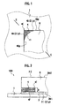
- Fig. 2 is a cross-sectional view taken along the face through the line segment II-II in Fig. 1 and cut perpendicularly to the paper.
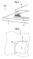
- Fig. 3 is a transparent perspective view for explaining the first embodiment of the present invention.
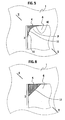
- Fig. 4 is a plan view for explaining an ideal shape of an edge portion of a semiconductor chip to avoid stress concentration, according to a first example of the first embodiment of the present invention.
- Fig. 5 is a transparent plan view for explaining a second example of the first embodiment of the present invention.
- Fig. 6 is a transparent plan view for explaining a third example of the first embodiment of the present invention.
- Fig. 7 is a transparent plan view for explaining a fourth example of the first embodiment of the present invention.
- Fig. 8 is a cross-sectional view for explaining a fifth example of the first embodiment of the present invention, taken along the face through the line segment IITV-IIIV in Fig. 9 and cut perpendicularly to the paper.
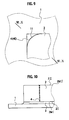
- Fig. 9 is a transparent plan view showing Fig. 8 or Fig. 10 from the top.
- Fig. 10 is a cross-sectional view for explaining a sixth example of the first embodiment of the present invention, taken along the face through the line segment X-X in Fig. 9 and cut perpendicularly to the paper.
- Fig. 11 is a transparent plan view for explaining a seventh example of the first embodiment of the present invention.
- Fig. 12 is a cross-sectional view taken along the face through the line segment XII-XII in Fig. 11 and cut perpendicularly to the paper.
- Fig. 13 is a cross-sectional view for explaining an eighth example of the first embodiment of the present invention.
- Fig. 14 is a cross-sectional view for explaining a ninth example of the first embodiment of the present invention.
- Fig. 15 is a cross-sectional view for explaining a tenth example of the first embodiment of the present invention.
- Fig. 16 is a cross-sectional view for explaining an eleventh example of the first embodiment of the present invention.
- Fig. 17 is a cross-sectional view for explaining a twelfth example of the first embodiment of the present invention.
- Fig. 18 is a view for explaining a second embodiment of the present invention.
- Fig. 19A, Fig. 19B and Fig. 19C are views for explaining a first manufacturing method the semiconductor device under the present invention.
- Fig. 20A, Fig. 20B and Fig. 20C are views for explaining a second manufacturing method of the semiconductor device under the present invention.
- Fig. 21A, Fig. 21B and Fig. 21C are views for explaining a third manufacturing method of the semiconductor device under the present invention.
- a first embodiment of the present invention is to be described below.
- the semiconductor chip 2 is made of single crystal semiconductor material(s) such as SiC, Si, Ge, GaAs and GaN.
- An active region is formed on a surface 2II (otherwise referred to as "second main face 2II") side or formed from the surface 2II to a backface 2I (otherwise referred to as "first main face 2I").
- the active region functioning such as transistor or diode (not shown in Fig. 1 to Fig. 3 ) is formed on the semiconductor chip 2.
- On the surface 2II of the semiconductor chip 2 there are one or more electrodes made from a second metallic thin film 2MII. The electrodes are respectively connected to corresponding external electrodes (not shown in Fig. 1 to Fig. 3 ).
- the details of the electronic device is to be omitted.
- a first metallic thin film 2MI is formed on the backface 2I (first main face 2I of semiconductor chip 2).
- the first metallic thin film 2MI enables the semiconductor chip 2 and the adhesive 3 to be bonded to each other.
- solder solder, braze, metallic paste made from silver particles, or a conductive adhesive may be used.
- the solder is used according to the first embodiment.
- the adhesive 3 may be referred to as solder 3.
- a crystalline defect region 4 is formed adjacent to the backface 2I at the edge portion of the semiconductor chip 2. Compared with a surrounding other semiconductor region 6, the crystalline defect region 4 is a region including more crystalline defects. Moreover, against the same amount of strain due to an external force, the strength of stress induced in the crystalline defect region 4 is smaller than that of stress induced in the other semiconductor region 6.
- the crystalline defect region 4 is an aggregation of the above regions.
- a method of forming the crystalline defect region 4 is to be described later.
- the crystalline defects existing in the crystalline defect region 4 may be present in the entire region drawn with hatching in the drawings ( Fig. 1 to Fig. 3 and the like) or may be locally present in a particular location (to be described afterward) in the crystalline defect region 4.
- the crystalline defect region 4 has a certain volume 4V defined as a pillar-like region having the following structure:
- bonding of the semiconductor chip 2 with the metallic substrate 1 is completed after heating the semiconductor chip 2 and the metallic substrate 1 to the solder 3's melting temperature or higher, placing the thus molten solder 3 between the semiconductor chip 2 and the metallic substrate 1, and thereafter deceasing the entire temperature to solidify the solder 3.
- the thermal expansion coefficients of the semiconductor chip 2 and the metallic substrate 1 are different from each other. Therefore, after the solder 3 is solidified, a stress is generated in a bonded region.
- the stress is concentrated especially in the edge portion of the semiconductor chip 2.
- Fig. 4 is a plan view for explaining an ideal shape of the edge portion of the semiconductor chip 2 to avoid the concentration of the stress induced from above-mentioned difference of thermal expansion coefficient between the metallic substrate 1 and the semiconductor chip 2. It is known that when the edge portion of the semiconductor chip 2 is rounded to have a circular arc being fit to the circle 13 in Fig. 4 , the stress concentration can be reduced considerably. In view of the current forming technology, however, it is highly difficult to realize such round edge shape.
- the crystalline defect region 4 is formed in the edge portion of the semiconductor chip 2.
- the difference of thermal expansion coefficients between the semiconductor chip 2 and the metallic substrate 1 causes a strain to the bonded portion especially to an edge portion of it.
- the crystalline defect region 4 can reduce the stress concentrated at the edge portion of the semiconductor chip 2.
- the stress in the bonded portion becomes closer to the one caused by the rounded edge portion in Fig. 4 , thus lowering a possibility of crack generation and deceasing degradation of heat-radiating performance.
- the lowered possibility of crack generation can bring about such an effect that the life of the bonded portion is elongated.
- the present technology has controlled the probability of such inconvenient phenomena caused by the crack not to fall the device's life span below the demanded value by taking a countermeasure such that the solder 3's thickness thicken to reduce the strain of the solder 3 with same deformation.
- this measure causes another demerit, that is, increase of electric and thermal resistance in the bonded region.
- the present invention can act the same role with avoiding these fault.
- the present invention capable of deceasing the adhesive (solder) 3's thickness can bring about such an effect that the electric resistance and heat resistance of the adhesive 3's layer can be decreased.
- the profile 4E may be a curve tangent to each of the first and second sides 4A, 4B which share the point 4C. Otherwise, the profile 4E may be a part of a polygon.
- Fig. 5 is a transparent plan view for explaining a second example of the first embodiment of the present invention.
- the profile 4E is a part of a polygon P.
- Fig. 6 is a transparent plan view for explaining a third example of the first embodiment of the present invention.
- Using a triangle shape as shown in Fig. 6 instead of the circular arc 13 shown in Fig. 4 is effective to a certain degree.
- the connecting line 11 is a straight line for connecting the first side 4A and the second side 4B which share the point 4C.
- Fig. 7 is a transparent plan view for explaining a fourth example of the first embodiment of the present invention.
- the profile 4E may also have a shape like a part of number 10 in Japanese kanji character which looks like a cross shape "+" (hereinafter, referred to as a cross region 2Ia).
- the curvature is larger at positions farther from a center O (equivalent to the point 4C) and an edge portion 4G of the crystalline defect region 4 is also in curve.
- the semiconductor chip 2 is cut out from a disc-like wafer. Forming the crystalline defect region 4 before cutting out the chip from the wafer is, as the case may be, more efficient. In such a case, a mark for cutting out the semiconductor chip 2 is generally made on a surface of the wafer, but the crystalline defect region 4 exists on a backface of the water. Hence, technically, some displacement must be allowed.
- the shape shown, in Fig. 7 is formed by rounding off the end portion 4G which is typically acute-angled.
- the shape in Fig. 7 can also bring about an effect that the displacement between the surface 2II and the backface 2I is allowed to a certain extent.
- the first method uses a technology including the following operations for forming a region including a large amount of crystalline defects:
- dot-like crystalline defect regions 4 may be effectively distributed in various fashions within the region of the edge portion.
- Fig. 8 is a cross-sectional view for explaining a fifth example of the first embodiment of the present invention, taken along the face through the line segment IIIV-IIIV in Fig. 9 and cut perpendicularly to the paper. As shown in Fig. 8 , approximately the same effect may be obtained by introducing crystalline defects from the backface 2I of the semiconductor chip 2 to a certain depth D1 along the profile 4E.
- the thick dotted line in Fig. 8 represents the crystalline defect region 4 and is introduced as shown in Fig. 9 in the plan view.
- Fig. 10 is a cross-sectional view for explaining a sixth example of the first embodiment of the present invention, taken along the face through the line segment X-X in Fig. 9 and cut perpendicularly to the paper.
- the crystalline defect regions 4 can be introduced to such an extent as to reach the surface 2II of the semiconductor chip 2 as shown in Fig. 10 .
- the edge portion may be separated due to extension of a crack, there will be no substantial problem since the semiconductor chip 2 is generally covered with some organic substance.
- Fig. 11 is a transparent plan view for explaining a seventh example of the first embodiment of the present invention.
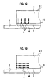
- the crystalline defect region 4 may be introduced in a plurality of lines in ripple-like shape as shown in Fig. 11 .
- Fig. 12 is a cross-sectional view taken along the face through the line segment XII-XII in Fig. 11 and cut perpendicularly to the paper.
- Fig. 13 is a cross-sectional view for explaining an eighth example of the first embodiment of the present invention. As shown in Fig. 13 , a plurality of crystalline defect regions 4 may be formed in parallel with the bottom face 4F (the first main face 2I). In this case, a corresponding plan view is Fig. 1 .
- Fig. 14 is a cross-sectional view for explaining a ninth example of the first embodiment of the present invention.
- the crystalline defect regions 4 may be so configured as to have a shape in Fig. 14.
- Fig. 14 is a combination of Fig. 8 and Fig. 13 .
- the edge portion is separated when the crack extends, which is, however, not a substantial problem.
- Fig. 15 is a cross-sectional view for explaining a tenth example of the first embodiment of the present invention.
- the shape of the crystalline defect region 4 is formed arbitrarily Therefore, the shape of the region tangent to the bottom face 4F of the crystalline defect region 4 (the backface 2I of the semiconductor chip 2) may be, for example, like the one shown in Fig. 9 , while the cross-sectional shape may be like the one shown in Fig. 15 .
- a second method of forming the crystalline defect region 4 introduces different types of materials.
- the second method includes the following operations for forming the crystalline defect region 4:
- any other materials may be used as long as such materials do not deform so much with some MPa
- the above materials are those capable of absorbing a possible strain caused by bending, plastic deforming or crack with a stress about 100 MPa.
- Fig. 16 is a cross-sectional view for explaining an eleventh example of the first embodiment of the present invention.
- a third method of forming the crystalline defect region 4 forms a groove 5.
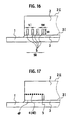
- a plurality of grooves 5 each having a depth 5D equal to or larger than a width 5W are formed in the first main face 2I of the semiconductor region 2, as shown in Fig. 16 .
- a region 50 where the grooves 5 are formed generates a smaller stress than a region where the grooves 5 are not formed. Moreover, the region 50 has the same effect as that brought about by the crystalline defect region 4.
- the region 50 where the grooves 5 are formed may be considered as a crystalline defect region which has an effect equivalent to that brought about by the crystalline defect region 4.
- the region 50 a part of crystal is missing.
- Fig. 17 is a cross-sectional view for explaining a twelfth example of the first embodiment of the present invention. Moreover, as shown in Fig. 17 , the grooves 5 may be arranged along the profile 4E of the crystalline defect region 4 and the crystalline defect regions 4 may be placed in parallel with the bottom face 4F (the first main face 2I) following Fig. 13 .
- the metallic substrate 1 is bonded via the adhesive 3 to the backface 2I of the semiconductor chip 2 having the edge portion.
- the semiconductor chip 2 includes the crystalline defect region 4 which includes the edge portion of the backface 2I, and the other semiconductor region 6 other than the crystalline defect region 4.
- the strength of stress induced in the crystalline defect region 4 is smaller than that of stress induced in the other semiconductor region 6.
- the presence of the crystalline defect region 4 can reduce the stress concentration considerably. As far as a stress in the bonded portion is concerned, it is closer to a state where a rounded shape of the edge portion is realized, thus obtaining an effect that a possibility of crack generation is lowered and degradation of heat-radiating performance is deceased.
- the lowered possibility of crack generation can bring about such an effect that the life of the bonded portion is elongated.
- the present technology has controlled the probability of such inconvenient phenomena caused by the crack not to fall the device's life span below the demanded value by taking a countermeasure such that the solder 3's thickness thicken to reduce the strain of the solder 3 with same deformation.
- this measure causes another demerit, that, is increase of electric and thermal resistance in the bonded region.
- the present invention can act the same role with avoiding these fault.
- the present invention capable of decreasing the adhesive (solder) 3's thickness can bring about such an effect that the electric resistance and heat resistance of the adhesive 3's layer can be decreased.
- the crystalline defect region 4 is formed to include more crystalline defects than the other semiconductor region 6, the crystalline defect region 4 can be formed according to a normal semiconductor manufacturing method, and realized inexpensively. Moreover, forming the grooves 5 can be realized easily and inexpensively by using a normal lithography technology.
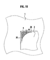
- Fig. 18 according to the second embodiment is a plan view based on Fig. 1 according to the first embodiment.
- forming the crystalline defect region 4 before cutting out the semiconductor chip 2 from the wafer process is, as the case may be, more efficient.
- the edge portion is formed slightly inside (for example, approximately 10 ⁇ m: defined as "certain distance D2") from an end 2E of the semiconductor chip 2 which is to be cut out.
- the method of placing the certain distance D2 between the end 2E of the semiconductor chip 2 and the crystalline defect region 4 can be applied to all the first to twelfth examples according to the first embodiment.
- the crystalline defect region 4 is so formed as to be away from the end 2E of the semiconductor chip 2 by the certain distance D2. Therefore, in addition to the effects brought about according to the first embodiment, the second embodiment can bring about the following effect: Before the crystalline defect region 4 exerts its original function, deformation or loss of a part of the crystalline defect region 4 can be avoided.
- a method of manufacturing the semiconductor device 100 under the present invention has the following sequential operations:
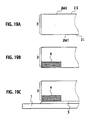
- FIG. 19A A first method of manufacturing the semiconductor device 100 shown in Fig. 2 is described referring to Fig. 19A, Fig. 19B and Fig. 19C .
- the crystalline defect region 4 is formed in a part (certain region) of the semiconductor chip 2 shown in Fig. 19A to thereby realize the state in Fig. 19B .
- the crystalline defect region 4 should be formed according to the second forming method including the following operations:
- FIG. 8 A second method of manufacturing the semiconductor device 100 shown in Fig. 8 is described referring to Fig. 20A, Fig. 20B and Fig. 20C .
- the crystalline defect region 4 is formed in a part (certain region) of the semiconductor chip 2 shown in Fig. 20A to thereby realize the state in Fig. 20B .
- the crystalline defect region 4 should be formed according to the first forming method including the following operations:
- FIG. 21A A third method of manufacturing the semiconductor device 100 shown in Fig. 16 is described referring to Fig. 21A, Fig. 21B and Fig. 21C .
- the crystalline defect region 4 is formed in a part (certain region) of the semiconductor chip 2 shown in Fig. 21A to thereby realize the state in Fig. 21B .
- the crystalline defect region should be formed according to the third method including the following operation:
Landscapes
- Internal Circuitry In Semiconductor Integrated Circuit Devices (AREA)
- Die Bonding (AREA)
- Dicing (AREA)
Abstract
Description
- The present invention relates to a semiconductor device and a method of manufacturing the semiconductor device.
- Japanese Patent Laid-Open Publication No.
Heisei 8(1996)-070069 JP8070069 - Note that, since the semiconductor chip and the solder do not bond to each other directly, a metallic thin film is formed on the backface of the semiconductor chip, and the metallic thin film and the metallic substrate are bonded to each other by the adhesive.
- It is an object of the present invention to provide a semiconductor device structure which can have longer lifetime with avoiding concentration of the stress in the bonded region between a semiconductor chip and a metallic substrate, and its manufacturing method.
- It is another object of the present invention to provide a method of manufacturing the above semiconductor device.
- According to a first aspect of the present invention, there is provided a semiconductor device comprising: a semiconductor chip including: a first main face having an edge portion, a second main face locating the opposite side to the first main face, a crystalline defect region present within a region of the edge portion and adjacent to the first main face, the crystalline region being configured to have a lower stress than the stress in the other semiconductor region for the same strain; and a metallic substrate to be bonded via a bonding member to the first main face of the semiconductor chip.
- According to a second aspect of the present invention, 16, there is provided a method of manufacturing the semiconductor device according to
claim 1, the method comprising: forming the crystalline defect region in a certain region of the semiconductor chip; forming a first metallic thin film on the first main face of the semiconductor chip which is in a state of being bonded to the metallic substrate; and bonding the metallic substrate to the first metallic thin film via the bonding member which is an adhesive. - Other objects and features of the present invention will become understood from the following description with reference to the accompanying drawings.
-
-
Fig. 1 is a transparent plan view for explaining a first embodiment of the present invention. -
Fig. 2 is a cross-sectional view taken along the face through the line segment II-II inFig. 1 and cut perpendicularly to the paper. -
Fig. 3 is a transparent perspective view for explaining the first embodiment of the present invention. -
Fig. 4 is a plan view for explaining an ideal shape of an edge portion of a semiconductor chip to avoid stress concentration, according to a first example of the first embodiment of the present invention. -
Fig. 5 is a transparent plan view for explaining a second example of the first embodiment of the present invention. -
Fig. 6 is a transparent plan view for explaining a third example of the first embodiment of the present invention. -
Fig. 7 is a transparent plan view for explaining a fourth example of the first embodiment of the present invention. -
Fig. 8 is a cross-sectional view for explaining a fifth example of the first embodiment of the present invention, taken along the face through the line segment IITV-IIIV inFig. 9 and cut perpendicularly to the paper. -
Fig. 9 is a transparent plan view showingFig. 8 orFig. 10 from the top. -
Fig. 10 is a cross-sectional view for explaining a sixth example of the first embodiment of the present invention, taken along the face through the line segment X-X inFig. 9 and cut perpendicularly to the paper. -
Fig. 11 is a transparent plan view for explaining a seventh example of the first embodiment of the present invention. -
Fig. 12 is a cross-sectional view taken along the face through the line segment XII-XII inFig. 11 and cut perpendicularly to the paper. -
Fig. 13 is a cross-sectional view for explaining an eighth example of the first embodiment of the present invention. -
Fig. 14 is a cross-sectional view for explaining a ninth example of the first embodiment of the present invention. -
Fig. 15 is a cross-sectional view for explaining a tenth example of the first embodiment of the present invention. -
Fig. 16 is a cross-sectional view for explaining an eleventh example of the first embodiment of the present invention. -
Fig. 17 is a cross-sectional view for explaining a twelfth example of the first embodiment of the present invention. -
Fig. 18 is a view for explaining a second embodiment of the present invention. -
Fig. 19A, Fig. 19B and Fig. 19C are views for explaining a first manufacturing method the semiconductor device under the present invention. -
Fig. 20A, Fig. 20B and Fig. 20C are views for explaining a second manufacturing method of the semiconductor device under the present invention. -
Fig. 21A, Fig. 21B and Fig. 21C are views for explaining a third manufacturing method of the semiconductor device under the present invention. - In the following, various embodiments of the present invention will be described in detail with reference to the accompanying drawings.
- For ease of understanding, the following description will include various directional terms, such as left, right, upper, lower, forward, rearward and the like. However, such terms are to be understood with respect to only a drawing or drawings on which the corresponding part of element is shown.
- A first embodiment of the present invention is to be described below.
-
-
Fig. 1 is a transparent plan view of asemiconductor device 100 under the present invention viewed from the top, depicting only an area in the vicinity of one edge portion of asemiconductor chip 2. -
Fig. 2 is a cross-sectional view taken along the face through the line segment II-II inFig. 1 and cut perpendicularly to the paper. -
Fig. 3 is a transparent perspective view of the area in the vicinity of the edge portion shown inFig. 1 . - The
semiconductor chip 2 is bonded onto a flat plate-shapedmetallic substrate 1 via an adhesive 3 serving as an adhesive member (= bonding member). - The
semiconductor chip 2 is made of single crystal semiconductor material(s) such as SiC, Si, Ge, GaAs and GaN. An active region is formed on a surface 2II (otherwise referred to as "second main face 2II") side or formed from the surface 2II to a backface 2I (otherwise referred to as "first main face 2I"). The active region functioning such as transistor or diode (not shown inFig. 1 to Fig. 3 ) is formed on thesemiconductor chip 2. On the surface 2II of thesemiconductor chip 2, there are one or more electrodes made from a second metallic thin film 2MII. The electrodes are respectively connected to corresponding external electrodes (not shown inFig. 1 to Fig. 3 ). In the description of the first embodiment, the details of the electronic device is to be omitted. - Moreover, since the
semiconductor chip 2 and the adhesive (bonding member) 3 do not bond to each other directly, a first metallic thin film 2MI is formed on the backface 2I (first main face 2I of semiconductor chip 2). The first metallic thin film 2MI enables thesemiconductor chip 2 and theadhesive 3 to be bonded to each other. - For the adhesive 3, solder, braze, metallic paste made from silver particles, or a conductive adhesive may be used. The solder is used according to the first embodiment. Hereinafter, the adhesive 3 may be referred to as
solder 3. - A
crystalline defect region 4 is formed adjacent to the backface 2I at the edge portion of thesemiconductor chip 2. Compared with a surroundingother semiconductor region 6, thecrystalline defect region 4 is a region including more crystalline defects. Moreover, against the same amount of strain due to an external force, the strength of stress induced in thecrystalline defect region 4 is smaller than that of stress induced in theother semiconductor region 6. - Otherwise, the
crystalline defect region 4 is an aggregation of the above regions. - A method of forming the
crystalline defect region 4 is to be described later. - Note that the crystalline defects existing in the
crystalline defect region 4 may be present in the entire region drawn with hatching in the drawings (Fig. 1 to Fig. 3 and the like) or may be locally present in a particular location (to be described afterward) in thecrystalline defect region 4. - In
Fig. 1, Fig. 2 andFig. 3 , thecrystalline defect region 4 has acertain volume 4V defined as a pillar-like region having the following structure: - 1) in the plan view of
Fig. 1 , afirst side line 4A and asecond side line 4B sharing apoint 4C, and aline 11 connecting to a first point 4Ap on thefirst side 4A and a second point 4Bp on thesecond side 4B forms as an outer periphery of abottom side area 4F which is a part of the first main face 2I, and - 2) in the side view of
Fig. 2 , a top side ofarea boundary 4T between thecrystalline defect region 4 and thesemiconductor region 6, which is apart from thebottom side area 4F with a distance D. - As described earlier, bonding of the
semiconductor chip 2 with themetallic substrate 1 is completed after heating thesemiconductor chip 2 and themetallic substrate 1 to thesolder 3's melting temperature or higher, placing the thusmolten solder 3 between thesemiconductor chip 2 and themetallic substrate 1, and thereafter deceasing the entire temperature to solidify thesolder 3. - The thermal expansion coefficients of the
semiconductor chip 2 and themetallic substrate 1 are different from each other. Therefore, after thesolder 3 is solidified, a stress is generated in a bonded region. - The stress is concentrated especially in the edge portion of the
semiconductor chip 2. The smaller the curvature radius of the edge portion is, the larger the intensity of the stress becomes.
Throughout the description of the present invention, it is thesemiconductor device 100's edge portion that is set forth in detail. -
Fig. 4 is a plan view for explaining an ideal shape of the edge portion of thesemiconductor chip 2 to avoid the concentration of the stress induced from above-mentioned difference of thermal expansion coefficient between themetallic substrate 1 and thesemiconductor chip 2. It is known that when the edge portion of thesemiconductor chip 2 is rounded to have a circular arc being fit to thecircle 13 inFig. 4 , the stress concentration can be reduced considerably. In view of the current forming technology, however, it is highly difficult to realize such round edge shape. - Therefore, the
crystalline defect region 4 is formed in the edge portion of thesemiconductor chip 2. As is mentioned above, the difference of thermal expansion coefficients between thesemiconductor chip 2 and themetallic substrate 1 causes a strain to the bonded portion especially to an edge portion of it. Thecrystalline defect region 4 can reduce the stress concentrated at the edge portion of thesemiconductor chip 2. - The stress in the bonded portion becomes closer to the one caused by the rounded edge portion in
Fig. 4 , thus lowering a possibility of crack generation and deceasing degradation of heat-radiating performance. - Also, the lowered possibility of crack generation can bring about such an effect that the life of the bonded portion is elongated.
- The present technology has controlled the probability of such inconvenient phenomena caused by the crack not to fall the device's life span below the demanded value by taking a countermeasure such that the
solder 3's thickness thicken to reduce the strain of thesolder 3 with same deformation. However, this measure causes another demerit, that is, increase of electric and thermal resistance in the bonded region. The present invention can act the same role with avoiding these fault. - In other words, the present invention capable of deceasing the adhesive (solder) 3's thickness can bring about such an effect that the electric resistance and heat resistance of the adhesive 3's layer can be decreased.
- Note that a
profile 4E (= the connecting line 11) of thecrystalline defect region 4, which is a circular arc inFig. 1 andFig. 3 , may have any shape as long as theprofile 4E gentles the curvature of the edge portion. Theprofile 4E may be a curve tangent to each of the first andsecond sides point 4C. Otherwise, theprofile 4E may be a part of a polygon. -
Fig. 5 is a transparent plan view for explaining a second example of the first embodiment of the present invention.
InFig. 5 , theprofile 4E is a part of a polygon P. -
Fig. 6 is a transparent plan view for explaining a third example of the first embodiment of the present invention.
Using a triangle shape as shown inFig. 6 instead of thecircular arc 13 shown inFig. 4 is effective to a certain degree. In this case, the connectingline 11 is a straight line for connecting thefirst side 4A and thesecond side 4B which share thepoint 4C. -
Fig. 7 is a transparent plan view for explaining a fourth example of the first embodiment of the present invention.
As shown inFig. 7 , theprofile 4E may also have a shape like a part of number 10 in Japanese kanji character which looks like a cross shape "+" (hereinafter, referred to as a cross region 2Ia). In this case, the curvature is larger at positions farther from a center O (equivalent to thepoint 4C) and anedge portion 4G of thecrystalline defect region 4 is also in curve. - The
semiconductor chip 2 is cut out from a disc-like wafer. Forming thecrystalline defect region 4 before cutting out the chip from the wafer is, as the case may be, more efficient. In such a case, a mark for cutting out thesemiconductor chip 2 is generally made on a surface of the wafer, but thecrystalline defect region 4 exists on a backface of the water. Hence, technically, some displacement must be allowed. - Forming the shape of the
crystalline defect region 4 as shown in each ofFig. 1 ,Fig. 5 and Fig. 6 its of difficulty. Therefore, the shape shown, inFig. 7 is formed by rounding off theend portion 4G which is typically acute-angled. The shape inFig. 7 can also bring about an effect that the displacement between the surface 2II and the backface 2I is allowed to a certain extent. - Next, first to third methods of forming the
crystalline defect region 4 are described below. - The first method uses a technology including the following operations for forming a region including a large amount of crystalline defects:
- 1) focusing, into the
semiconductor chip 2, a laser beam having a wavelength to be absorbed by thesemiconductor chip 2, - 2) instantaneously heating dot-like regions within a region including the edge portion of the first main face 2I, and
- 3) instantaneously quenching the dot-like regions.
- The above operations form a structure where the crack is generated only in the
crystalline defect region 4 with a relatively small stress. As a result, the extension of cracks is limited within theprofile 4E. - Note that dot-like
crystalline defect regions 4 may be effectively distributed in various fashions within the region of the edge portion. -
Fig. 8 is a cross-sectional view for explaining a fifth example of the first embodiment of the present invention, taken along the face through the line segment IIIV-IIIV inFig. 9 and cut perpendicularly to the paper.
As shown inFig. 8 , approximately the same effect may be obtained by introducing crystalline defects from the backface 2I of thesemiconductor chip 2 to a certain depth D1 along theprofile 4E. The thick dotted line inFig. 8 represents thecrystalline defect region 4 and is introduced as shown inFig. 9 in the plan view. -
Fig. 10 is a cross-sectional view for explaining a sixth example of the first embodiment of the present invention, taken along the face through the line segment X-X inFig. 9 and cut perpendicularly to the paper.
Alternatively, thecrystalline defect regions 4 can be introduced to such an extent as to reach the surface 2II of thesemiconductor chip 2 as shown inFig. 10 . In this case, although the edge portion may be separated due to extension of a crack, there will be no substantial problem since thesemiconductor chip 2 is generally covered with some organic substance. -
Fig. 11 is a transparent plan view for explaining a seventh example of the first embodiment of the present invention.
Alternatively, thecrystalline defect region 4 may be introduced in a plurality of lines in ripple-like shape as shown inFig. 11 . -
Fig. 12 is a cross-sectional view taken along the face through the line segment XII-XII inFig. 11 and cut perpendicularly to the paper. -
Fig. 13 is a cross-sectional view for explaining an eighth example of the first embodiment of the present invention,
As shown inFig. 13 , a plurality ofcrystalline defect regions 4 may be formed in parallel with thebottom face 4F (the first main face 2I). In this case, a corresponding plan view isFig. 1 . -
Fig. 14 is a cross-sectional view for explaining a ninth example of the first embodiment of the present invention.
Alternatively, thecrystalline defect regions 4 may be so configured as to have a shape inFig. 14. Fig. 14 is a combination ofFig. 8 andFig. 13 . In this case too, the edge portion is separated when the crack extends, which is, however, not a substantial problem. -
Fig. 15 is a cross-sectional view for explaining a tenth example of the first embodiment of the present invention.
In the first method using the technology for introducing the dot-likecrystalline defect regions 4, the shape of thecrystalline defect region 4 is formed arbitrarily
Therefore, the shape of the region tangent to thebottom face 4F of the crystalline defect region 4 (the backface 2I of the semiconductor chip 2) may be, for example, like the one shown inFig. 9 , while the cross-sectional shape may be like the one shown inFig. 15 . - A second method of forming the
crystalline defect region 4 introduces different types of materials. - For example, in a process before cutting out the
semiconductor chip 2 from the wafer, the second method includes the following operations for forming the crystalline defect region 4: - 1) forming a shallow groove in the backface of the wafer, as depicted by the cross region 2Ia drawn with the hatching in
Fig. 7 , - 2) by means of a CVD (Chemical Vapor Deposition) or the like, depositing, in the shallow groove, different types of materials such as polycrystalline semiconductor, amorphous semiconductor, PSG (phosphosilicate glass) and the like, and
- 3) flattening the portion where the shallow groove is formed.
- Any other materials may be used as long as such materials do not deform so much with some MPa Specifically, the above materials are those capable of absorbing a possible strain caused by bending, plastic deforming or crack with a stress about 100 MPa.
-
Fig. 16 is a cross-sectional view for explaining an eleventh example of the first embodiment of the present invention.
A third method of forming thecrystalline defect region 4 forms agroove 5.
Following the plan view ofFig. 11 , a plurality ofgrooves 5 each having adepth 5D equal to or larger than awidth 5W are formed in the first main face 2I of thesemiconductor region 2, as shown inFig. 16 . - Against the same strain due to an external force, a
region 50 where thegrooves 5 are formed generates a smaller stress than a region where thegrooves 5 are not formed. Moreover, theregion 50 has the same effect as that brought about by thecrystalline defect region 4. - In other words, the
region 50 where thegrooves 5 are formed may be considered as a crystalline defect region which has an effect equivalent to that brought about by thecrystalline defect region 4. In theregion 50, a part of crystal is missing. In this case, it is preferable to set thedepth 5D of each of thegrooves 5 to equal to or larger than twice aninterval 5I between ends of thegrooves 5. -
Fig. 17 is a cross-sectional view for explaining a twelfth example of the first embodiment of the present invention.
Moreover, as shown inFig. 17 , thegrooves 5 may be arranged along theprofile 4E of thecrystalline defect region 4 and thecrystalline defect regions 4 may be placed in parallel with thebottom face 4F (the first main face 2I) followingFig. 13 . - In some processes for forming the
grooves 5, a part of the first metallic thin film 2MI necessary for soldering (solder 3) is put in thegrooves 5. In the above processes, however, whether the first metallic thin film 2MI is put in thegrooves 5 or not does not influence the effect so much. - As described so far, according to the first embodiment, the
metallic substrate 1 is bonded via the adhesive 3 to the backface 2I of thesemiconductor chip 2 having the edge portion. Thesemiconductor chip 2 includes thecrystalline defect region 4 which includes the edge portion of the backface 2I, and theother semiconductor region 6 other than thecrystalline defect region 4. - Moreover, against the same amount of strain due to an external force, the strength of stress induced in the
crystalline defect region 4 is smaller than that of stress induced in theother semiconductor region 6. - Therefore, the presence of the
crystalline defect region 4 can reduce the stress concentration considerably. As far as a stress in the bonded portion is concerned, it is closer to a state where a rounded shape of the edge portion is realized, thus obtaining an effect that a possibility of crack generation is lowered and degradation of heat-radiating performance is deceased. - Furthermore, in the backface 2I of the
semiconductor chip 2 within the region including the edge portion, forming thegroove 5 having thedepth 5D equal to or larger than thewidth 5W can bring about the same effects as above. - Also, the lowered possibility of crack generation can bring about such an effect that the life of the bonded portion is elongated.
- The present technology has controlled the probability of such inconvenient phenomena caused by the crack not to fall the device's life span below the demanded value by taking a countermeasure such that the
solder 3's thickness thicken to reduce the strain of thesolder 3 with same deformation. However, this measure causes another demerit, that, is increase of electric and thermal resistance in the bonded region. The present invention can act the same role with avoiding these fault. - In other words, the present invention capable of decreasing the adhesive (solder) 3's thickness can bring about such an effect that the electric resistance and heat resistance of the adhesive 3's layer can be decreased.
- Furthermore, since the
crystalline defect region 4 is formed to include more crystalline defects than theother semiconductor region 6, thecrystalline defect region 4 can be formed according to a normal semiconductor manufacturing method, and realized inexpensively. Moreover, forming thegrooves 5 can be realized easily and inexpensively by using a normal lithography technology. - Next, a second embodiment of the present invention is to be described.
-
Fig. 18 according to the second embodiment is a plan view based onFig. 1 according to the first embodiment. As stated earlier, forming thecrystalline defect region 4 before cutting out thesemiconductor chip 2 from the wafer process is, as the case may be, more efficient. In such a case, in order to prevent thecrystalline defect region 4, which is vulnerable to an external force, from being affected by the external force in the cutting-out process, the edge portion is formed slightly inside (for example, approximately 10 µm: defined as "certain distance D2") from anend 2E of thesemiconductor chip 2 which is to be cut out. By forming thecrystalline defect region 4 in the above configuration, deformation or loss of a part of thecrystalline defect region 4 before exerting the original function thereof is avoided. - Note that the method of placing the certain distance D2 between the
end 2E of thesemiconductor chip 2 and thecrystalline defect region 4 can be applied to all the first to twelfth examples according to the first embodiment. - As described above, according to the second embodiment, the
crystalline defect region 4 is so formed as to be away from theend 2E of thesemiconductor chip 2 by the certain distance D2. Therefore, in addition to the effects brought about according to the first embodiment, the second embodiment can bring about the following effect: Before thecrystalline defect region 4 exerts its original function, deformation or loss of a part of thecrystalline defect region 4 can be avoided. - A method of manufacturing the
semiconductor device 100 under the present invention has the following sequential operations: - 1) a first operation of forming the
crystalline defect region 4 in a certain region of thesemiconductor chip 2, - 2) a second operation of forming the first metallic thin film 2MI on the first main face 2I which is in a state before being bonded to the
metallic substrate 1, and - 3) a third operation of bonding the
metallic substrate 1 and the first metallic thin film 2MI to each other. - A first method of manufacturing the
semiconductor device 100 shown inFig. 2 is described referring toFig. 19A, Fig. 19B and Fig. 19C . - The
crystalline defect region 4 is formed in a part (certain region) of thesemiconductor chip 2 shown inFig. 19A to thereby realize the state inFig. 19B . In this case, thecrystalline defect region 4 should be formed according to the second forming method including the following operations: - 1) forming a shallow groove in a certain portion (cross region 2Ia) of the first main face 2I,
- 2) depositing, in the shallow groove, a material different from a semiconductor material that is a constituent of the
semiconductor chip 2, and - 3) flattening the certain portion (cross region 2Ia) where the shallow groove is formed
- Next, after the forming of the first metallic thin film 2MI on the backface 2I of the
semiconductor chip 2, the following operations are implemented: - 1) placing the adhesive 3 between the backface 2I of the
semiconductor chip 2 and themetallic substrate 1, - 2) heating all components to equal to or higher than the melting temperature of the adhesive 3,
- 3) decreasing the temperature back to room temperature, and
- 4) accomplishing the state of
Fig. 19C , in other words, a state where thesemiconductor device 100 shown inFig. 2 is completed. - A second method of manufacturing the
semiconductor device 100 shown inFig. 8 is described referring toFig. 20A, Fig. 20B and Fig. 20C . - The
crystalline defect region 4 is formed in a part (certain region) of thesemiconductor chip 2 shown inFig. 20A to thereby realize the state inFig. 20B . In this case, thecrystalline defect region 4 should be formed according to the first forming method including the following operations: - 1) focusing, into the
semiconductor chip 2, a laser beam having a wavelength to be absorbed by thesemiconductor chip 2, - 2) instantaneously heating the dot-like regions, and
- 3) instantaneously quenching the dot-like regions.
- Next, after the forming of the first metallic thin film 2MI on the backface 2I of the
semiconductor chip 2, the following operations are implemented: - 1) placing the adhesive 3 between the backface 2I of the
semiconductor chip 2 and themetallic substrate 1, - 2) heating all components to equal to or higher than the melting temperature of the adhesive 3,
- 3) decreasing the temperature back to room temperature, and
- 4) accomplishing the state of
Fig. 20C , in other words, a state where thesemiconductor device 100 shown inFig. 8 is completed. - A third method of manufacturing the
semiconductor device 100 shown inFig. 16 is described referring toFig. 21A, Fig. 21B and Fig. 21C . - The
crystalline defect region 4 is formed in a part (certain region) of thesemiconductor chip 2 shown inFig. 21A to thereby realize the state inFig. 21B . In this case, the crystalline defect region should be formed according to the third method including the following operation: - 1) forming the
groove 5 in the first main face 2I of thesemiconductor chip 2, such that thedepth 5D of thegroove 5 is equal to or larger than thewidth 5W of thegroove 5. - 1) placing the adhesive 3 between the backface 2I of the
semiconductor chip 2 and themetallic substrate 1, - 2) heating all components to equal to or higher than the melting temperature of the adhesive 3,
- 3) decreasing the temperature back to room temperature, and
- 4) accomplishing the state of
Fig. 21C , in other words, a state where thesemiconductor device 100 shown inFig. 16 is completed. - Although the present invention has been described above by reference to certain embodiments, the present invention is not limited to the embodiments described above. Modifications and variations of the embodiments described above will occur to those skilled in the art, in light of the above teachings.
- This application is based on a prior Japanese Patent Application Nos.
P2007-058505 (filed on March 8, 2007 P2007-278693 (filed on October 26, 2007 P2007-058505 P2007-278693 - The scope of the present invention is defined with reference to the following claims.
Claims (20)
- A semiconductor device (100) comprising:a semiconductor chip (2) including:a first main face (2I) having an edge portion,a second main face (2II) locating the opposite side to the first main face (2I),a crystalline defect region (4, 5) present within a region of the edge portion and adjacent to the first main face (2I) the crystalline region (4, 5) being configured to have a lower stress than the stress in the other semiconductor region (6) for the same strain; anda metallic substrate (1) to be bonded via a bonding member (3) to the first main face (2I) of the semiconductor chip (2).
- The semiconductor device (100) according to claim 1, wherein
the crystalline defect region (4) is a region or an aggregation of the regions including more crystalline defects than the other semiconductor region (6). - The semiconductor device (100) according to any of claims 1 and 2, wherein
the crystalline defect region (4) has a certain volume (4V) defined by as a pillar-like region (4) having:a bottom area (4F) being defined its periphery by a first side edge (4A) and a second side edge (4B) which are a part of the periphery of the first main face (2I) respectively, and a line (11) in the first main face (2I) connecting a first point (4Ap) on the first side (4A) with a second point (4Bp) on the second side (4B); anda height (D) of the pillar (4) of which height (4) being not larger than a thickness of the semiconductor chip (2). - The semiconductor device (100) according to claim 3, wherein
the connecting line (11) has a circular arc (13) tangent to the first side (4A) at the first point (4Ap) and the second side (4B) at the second point (4Bp). - The semiconductor device (100) according to claim 3, wherein
the connecting line (11) is a straight line for connecting the first side (4A) at the first point (4Ap) and the second side (4B) at the second point (4Bp). - The semiconductor device (100) according to claim 3, wherein
the connecting line (11) is a plurality of straight lines each of which is a part of a polygon (P). - The semiconductor device (100) according to claim 1, wherein
the crystalline defect region (4, 5) includes at least one groove (5) formed in the fust main face (2I) of the semiconductor chip (2), and
a depth (5D) of the groove (5) is equal to or larger than a width (5W) of the groove (5). - The semiconductor device (100) according to claim 7, wherein
the depth (5D) of the groove (5) is equal to or larger than twice an interval (5I) between ends of the grooves (5). - The semiconductor device (100) according to any of claims 1 to 5, wherein
the crystalline defect region (4) is formed inside the semiconductor chip (2) away from side faces of the semiconductor chip (2), by a certain distance (D2), and each side face shares an edge line (2E) with the first main face (2I). - The semiconductor device (100) according to claim 9, wherein
the certain distance (D2) is approximately 10 µm. - The semiconductor device (100) according to any of claims 3 to 5, wherein
a plurality of the crystalline defect regions (4) are formed to be reached to the first main face (2I) and to be along the connecting line (11) perpendicularly to the first main face (2I). - The semiconductor device (100) according to any of claims 1 to 5, wherein
the crystalline defect region (4) is formed in a substantially planer shape in parallel with the first main face (2I). - The semiconductor device (100) according to claim 1, wherein
the crystalline defect region (4) is configured to be formed by the following operations:focusing, into the semiconductor chip (2), a laser beam having a wavelength to be absorbed by the semiconductor chip (2),heating a dot-like region within a region including the edge portion of the first main face (2I), andquenching the dot-like region. - The semiconductor device (100) according to claim 1, wherein
the crystalline defect region (4) is configured to be formed by the following operations:forming a groove in a certain portion (2Ia) of the first main face (2I),depositing, in the groove, a material different from a semiconductor material which is a constituent of the semiconductor chip (2), andflattening the certain portion (2Ia) of the first main face (2I). - The semiconductor device (100) according to claim 14, wherein
the certain portion (2Ia) of the first main face (2I) is a cross region (2Ia) on a backface of a wafer. - A method of manufacturing the semiconductor device (100) according to claim 1, the method comprising:forming the crystalline defect region (4, 5) in a certain region of the semiconductor chip (2);forming a first metallic thin film (2MI) on the first main face (2I) of the semiconductor chip (2) which is in a state of being bonded to the metallic substrate (1); andbonding the metallic substrate (1) to the first metallic thin film (2MI) via the bonding member (3) which is an adhesive (3).
- The method of manufacturing the semiconductor device (100) according to claim. 16, further comprising the following operations for forming the crystalline defect region (4, 5):focusing, into the semiconductor chip (2), a laser beam having a wavelength to be absorbed by the semiconductor chip (2),heating a dot-like region within a region including the edge portion of the first main face (2I), andquenching the dot-like region.
- The method of manufacturing the semiconductor device (100) according to claim 16, further comprising the following operations for forming the crystalline defect region (4, 5):forming a groove in a certain portion (2Ia) of the first main face (2I),depositing in the groove a material different from a semiconductor material which is a constituent of the semiconductor chip (2), andflattening the certain portion (2Ia) of the first main face (2I).
- The method of manufacturing the semiconductor device (100) according to claim 16, further comprising the following operation for forming the crystalline defect region (4,5):forming a groove (5) in the first main face (2I) of the semiconductor chip (2), such that a depth (5D) of the groove (5) is equal to or larger than a width (5W) of the groove (5).
- The method of manufacturing the semiconductor device (100) according to claim 19, wherein
the depth (5D) of the groove (5) is equal to or larger than twice an interval (5I) between ends of the grooves (5).
Applications Claiming Priority (2)
| Application Number | Priority Date | Filing Date | Title |
|---|---|---|---|
| JP2007058505 | 2007-03-08 | ||
| JP2007278693A JP5251073B2 (en) | 2007-03-08 | 2007-10-26 | Semiconductor device and manufacturing method thereof |
Publications (2)
| Publication Number | Publication Date |
|---|---|
| EP1968109A2 true EP1968109A2 (en) | 2008-09-10 |
| EP1968109A3 EP1968109A3 (en) | 2012-08-01 |
Family
ID=39463136
Family Applications (1)
| Application Number | Title | Priority Date | Filing Date |
|---|---|---|---|
| EP08004084A Withdrawn EP1968109A3 (en) | 2007-03-08 | 2008-03-05 | Semiconductor device and method of manufacturing the same |
Country Status (2)
| Country | Link |
|---|---|
| US (1) | US8575726B2 (en) |
| EP (1) | EP1968109A3 (en) |
Families Citing this family (2)
| Publication number | Priority date | Publication date | Assignee | Title |
|---|---|---|---|---|
| US9496193B1 (en) * | 2015-09-18 | 2016-11-15 | Infineon Technologies Ag | Semiconductor chip with structured sidewalls |
| TWI669789B (en) * | 2016-04-25 | 2019-08-21 | 矽品精密工業股份有限公司 | Electronic package |
Citations (1)
| Publication number | Priority date | Publication date | Assignee | Title |
|---|---|---|---|---|
| JPH0870069A (en) | 1994-08-30 | 1996-03-12 | Hitachi Ltd | Semiconductor device |
Family Cites Families (12)
| Publication number | Priority date | Publication date | Assignee | Title |
|---|---|---|---|---|
| JPH04312933A (en) | 1991-03-29 | 1992-11-04 | Mitsubishi Electric Corp | Semiconductor device |
| US6225695B1 (en) * | 1997-06-05 | 2001-05-01 | Lsi Logic Corporation | Grooved semiconductor die for flip-chip heat sink attachment |
| US5955781A (en) * | 1998-01-13 | 1999-09-21 | International Business Machines Corporation | Embedded thermal conductors for semiconductor chips |
| JP2001338947A (en) * | 2000-05-26 | 2001-12-07 | Nec Corp | Flip chip type semiconductor device and manufacturing method thereof |
| JP2002237454A (en) * | 2001-02-08 | 2002-08-23 | Seiko Epson Corp | Manufacturing method of thin film semiconductor |
| US7498608B2 (en) * | 2001-10-29 | 2009-03-03 | Sharp Kabushiki Kaisha | Nitride-composite semiconductor laser element, its manufacturing method, and semiconductor optical device |
| US7462882B2 (en) * | 2003-04-24 | 2008-12-09 | Sharp Kabushiki Kaisha | Nitride semiconductor light-emitting device, method of fabricating it, and semiconductor optical apparatus |
| DE10341186A1 (en) * | 2003-09-06 | 2005-03-31 | Martin Michalk | Method and device for contacting semiconductor chips |
| JP4461767B2 (en) | 2003-10-16 | 2010-05-12 | 株式会社ブリヂストン | Anisotropic conductive film |
| JP2005150220A (en) | 2003-11-12 | 2005-06-09 | Seiko Epson Corp | Semiconductor device, semiconductor wafer, and manufacturing method thereof |
| JP4340578B2 (en) * | 2004-04-09 | 2009-10-07 | 富士通株式会社 | Component mounting board and component mounting structure |
| JP4759948B2 (en) * | 2004-07-28 | 2011-08-31 | ルネサスエレクトロニクス株式会社 | Manufacturing method of semiconductor device |
-
2008
- 2008-03-05 EP EP08004084A patent/EP1968109A3/en not_active Withdrawn
- 2008-03-06 US US12/073,489 patent/US8575726B2/en not_active Expired - Fee Related
Patent Citations (1)
| Publication number | Priority date | Publication date | Assignee | Title |
|---|---|---|---|---|
| JPH0870069A (en) | 1994-08-30 | 1996-03-12 | Hitachi Ltd | Semiconductor device |
Non-Patent Citations (2)
| Title |
|---|
| "CHAPTER 4: Material property charts ED - Ashby M F", 1 January 2005, MATERIALS SELECTION IN MECHANICAL DESIGN, AMSTERDAM [U.A.] : ELSEVIER BUTTERWORTH-HEINEMANN, PAGE(S) 45 - 78, ISBN: 978-0-7506-6168-3, XP007922204 * |
| ANONYMOUS: "Crystallographic defect - Wikipedia, the free encyclopedia", 16 August 2016 (2016-08-16), XP055296797, Retrieved from the Internet <URL:https://en.wikipedia.org/wiki/Crystallographic_defect> [retrieved on 20160822] * |
Also Published As
| Publication number | Publication date |
|---|---|
| EP1968109A3 (en) | 2012-08-01 |
| US20080217744A1 (en) | 2008-09-11 |
| US8575726B2 (en) | 2013-11-05 |
Similar Documents
| Publication | Publication Date | Title |
|---|---|---|
| CN107256903B (en) | Metal foil pattern laminate, metal foil laminate, metal foil laminate substrate, solar cell module, and manufacturing method thereof | |
| CN102891231B (en) | Method for manufacturing light-emitting device | |
| US8859307B2 (en) | Semiconductor device and method for manufacturing same | |
| US20150217400A1 (en) | Method for cutting object to be processed | |
| EP2922156B1 (en) | Semiconductor laser light source | |
| EP1850400A1 (en) | Light-emitting element and method for manufacturing light-emitting element | |
| EP1947703B1 (en) | Interconnector, solar battery string using such interconnector | |
| KR20220156662A (en) | Solar cell interconnection | |
| TW201248870A (en) | Solar cell | |
| JP2015012244A (en) | Semiconductor light-emitting element | |
| US10707389B2 (en) | Light emitting device | |
| CN113369677A (en) | Wafer cutting method and cutting equipment | |
| CN104167389A (en) | Semiconductor devices having a glass substrate, and method for manufacturing thereof | |
| US7276740B2 (en) | Submount for light emitting device | |
| EP3872876B1 (en) | Semiconductor device | |
| US8575726B2 (en) | Semiconductor device and method of manufacturing the same | |
| US10497843B2 (en) | Light emitting device | |
| TW201530825A (en) | Method for arranging light-emitting diode crystal grains of different shapes or different sizes in a sub-base | |
| TW201532303A (en) | Method for stress-induced cutting semiconductor device | |
| CN104112729A (en) | Method For Manufacturing Semiconductor Devices Having A Glass Substrate | |
| US20100084002A1 (en) | Method for manufacturing a solderable lfc solar cell rear side and a solar module from such connected lfc solar cells | |
| US8537867B2 (en) | Method for fabricating optical device | |
| US20050275114A1 (en) | Semiconductor device and semiconductor apparatus | |
| CN1370306A (en) | Device and method for making devices comprising at least chip mounted on support | |
| CN108475898A (en) | Semiconductor laser and the method for manufacturing semiconductor laser and wafer |
Legal Events
| Date | Code | Title | Description |
|---|---|---|---|
| PUAI | Public reference made under article 153(3) epc to a published international application that has entered the european phase |
Free format text: ORIGINAL CODE: 0009012 |
|
| 17P | Request for examination filed |
Effective date: 20080305 |
|
| AK | Designated contracting states |
Kind code of ref document: A2 Designated state(s): AT BE BG CH CY CZ DE DK EE ES FI FR GB GR HR HU IE IS IT LI LT LU LV MC MT NL NO PL PT RO SE SI SK TR |
|
| AX | Request for extension of the european patent |
Extension state: AL BA MK RS |
|
| PUAL | Search report despatched |
Free format text: ORIGINAL CODE: 0009013 |
|
| AK | Designated contracting states |
Kind code of ref document: A3 Designated state(s): AT BE BG CH CY CZ DE DK EE ES FI FR GB GR HR HU IE IS IT LI LT LU LV MC MT NL NO PL PT RO SE SI SK TR |
|
| AX | Request for extension of the european patent |
Extension state: AL BA MK RS |
|
| RIC1 | Information provided on ipc code assigned before grant |
Ipc: H01L 23/14 20060101ALI20120628BHEP Ipc: H01L 29/32 20060101ALI20120628BHEP Ipc: H01L 29/06 20060101ALI20120628BHEP Ipc: H01L 23/00 20060101ALI20120628BHEP Ipc: H01L 21/60 20060101AFI20120628BHEP |
|
| AKX | Designation fees paid |
Designated state(s): DE FR GB |
|
| 17Q | First examination report despatched |
Effective date: 20140116 |
|
| STAA | Information on the status of an ep patent application or granted ep patent |
Free format text: STATUS: EXAMINATION IS IN PROGRESS |
|
| STAA | Information on the status of an ep patent application or granted ep patent |
Free format text: STATUS: THE APPLICATION IS DEEMED TO BE WITHDRAWN |
|
| 18D | Application deemed to be withdrawn |
Effective date: 20170106 |