EP1967371A1 - Light amount control, optical writing, and image forming apparatuses - Google Patents
Light amount control, optical writing, and image forming apparatuses Download PDFInfo
- Publication number
- EP1967371A1 EP1967371A1 EP08152256A EP08152256A EP1967371A1 EP 1967371 A1 EP1967371 A1 EP 1967371A1 EP 08152256 A EP08152256 A EP 08152256A EP 08152256 A EP08152256 A EP 08152256A EP 1967371 A1 EP1967371 A1 EP 1967371A1
- Authority
- EP
- European Patent Office
- Prior art keywords
- amount
- light
- value
- drive current
- unit
- Prior art date
- Legal status (The legal status is an assumption and is not a legal conclusion. Google has not performed a legal analysis and makes no representation as to the accuracy of the status listed.)
- Granted
Links
- 230000003287 optical effect Effects 0.000 title claims abstract description 19
- 238000006243 chemical reaction Methods 0.000 claims 8
- 238000013459 approach Methods 0.000 claims 2
- 238000000034 method Methods 0.000 description 40
- 239000003990 capacitor Substances 0.000 description 12
- 238000010586 diagram Methods 0.000 description 8
- 238000012544 monitoring process Methods 0.000 description 6
- 101100115778 Caenorhabditis elegans dac-1 gene Proteins 0.000 description 5
- 238000005070 sampling Methods 0.000 description 4
- 230000003247 decreasing effect Effects 0.000 description 1
- 229920005994 diacetyl cellulose Polymers 0.000 description 1
- 238000007599 discharging Methods 0.000 description 1
- 238000012986 modification Methods 0.000 description 1
- 230000004048 modification Effects 0.000 description 1
Images




Classifications
-
- B—PERFORMING OPERATIONS; TRANSPORTING
- B41—PRINTING; LINING MACHINES; TYPEWRITERS; STAMPS
- B41J—TYPEWRITERS; SELECTIVE PRINTING MECHANISMS, i.e. MECHANISMS PRINTING OTHERWISE THAN FROM A FORME; CORRECTION OF TYPOGRAPHICAL ERRORS
- B41J2/00—Typewriters or selective printing mechanisms characterised by the printing or marking process for which they are designed
- B41J2/435—Typewriters or selective printing mechanisms characterised by the printing or marking process for which they are designed characterised by selective application of radiation to a printing material or impression-transfer material
- B41J2/447—Typewriters or selective printing mechanisms characterised by the printing or marking process for which they are designed characterised by selective application of radiation to a printing material or impression-transfer material using arrays of radiation sources
- B41J2/45—Typewriters or selective printing mechanisms characterised by the printing or marking process for which they are designed characterised by selective application of radiation to a printing material or impression-transfer material using arrays of radiation sources using light-emitting diode [LED] or laser arrays
Definitions
- the present invention relates to a light amount control apparatus for a light source used in optical writing, an optical writing apparatus with the light amount control apparatus, and an image forming apparatus with the optical writing apparatus.
- a laser diode is generally used as a writing light source for a printing device such as a printer or copier.
- the laser diode used as an optical writing light source requires that a light emission amount be kept to a constant value for making the density of a generated image constant.
- JP2001-138566A discloses, for keeping a light amount of a laser diode (LD) constant, detecting at a photodetecting device (PD) housed in the same package as the LD light from the LD, and using a monitoring current generated at the detecting PD to control the light amount to be constant.
- LD laser diode
- PD photodetecting device
- the monitoring current generated at the PD due to the detected light passes through a light-amount setting variable resistor so as to be converted to a monitoring voltage, which is input to a comparator so as to be compared with a reference voltage and controls the voltage of a hold capacitor.
- the process is performed such that, with a sample-and-hold signal input to a control circuit in the sample mode, the monitoring and reference voltages are compared so that when "the monitoring voltage > the reference voltage", a current passes through the hold capacitor from a constant discharging current source so as to cause a voltage drop across the hold capacitor; when "the monitoring voltage ⁇ the reference voltage", a current passes through the hold capacitor from a constant charging current source so as to cause a voltage rise across the hold capacitor.
- the constant current source is disconnected from the hold capacitor.
- the terminal voltage of the hold capacitor is input to a differential amplifier, causing a current supplied to the LD to be increased or decreased according to the difference with the reference voltage.
- a series of control loops as described above allows the light emission amount of the LD to be kept constant.
- JP2003-266774A discloses an image-forming apparatus using a VCSEL with 32 light-emitting points.
- a problem to be solved by the present invention is to ensure control sufficient to keep the light amount constant, and to ensure control sufficient to keep the light amount constant even with, especially, a light source with a large number of light-emitting points.
- Embodiments according to the present invention are described, referring to FIG. 1 through FIG. 10 .
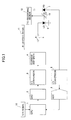
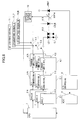
- FIG. 1 is a block diagram illustrating a circuit configuration of a light amount control apparatus according to a first embodiment of the invention.
- the light amount control apparatus basically includes a CPU 1, a DAC (digital/analog converter) 2, a V/I (voltage/current) converter 3, a current amplifier 4, a switching element 5, a LD (laser diode) 6, a PD (photodiode) 7, an I/V (current/voltage) converter 8, and an ADC (analog/digital converter) 9.
- the CPU 1 sets a DAC code corresponding to a LD drive current in the DAC 2 based on a sample-and-hold signal 10 input from a sample-and-hold circuit (not shown).
- the DAC 2 outputs a voltage according to the set DAC code.
- the voltage output from the DAC 2 is converted at the V/I converter 3 to a current, which is input to the current amplifier 4.
- a current output from the current amplifier 4 is supplied to the LD 6, which turns on at a light amount according to the current.
- a light output from the LD 6 is divided with a half mirror 14 into two beams, one of which is input to the PD 7 as a photodetector. The other is directed to a recording medium 12 of the image forming apparatus body.
- the beam input to the PD 7 is converted to a current, which, at the I/V converter 8, is converted to a voltage, which is input to the ADC 9.
- the converted digital output of the ADC 9 is input to the CPU 1.
- the CPU 1 compares the converted digital value input from the ADC 9 with a predetermined target digital value, and computes a new DAC code such that the converted digital input and the target digital value match. Thereafter, the CPU 1 sets a new DAC code in the DAC 2.
- Executing such a series of control loops as described above allows keeping an output light amount of the LD 6 at the predetermined target value.
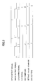
- FIG. 2 is a timing chart illustrating timings of controlling the light amount while outputting an image.
- the timing chart shows output timings of a sync detect signal, an image output period, a LD lighting signal, a sample-and-hold (S/H) signal, an ADC sampling signal, a setting-value compute signal, and a DAC setting signal.
- the sync detect signal which is for setting a write-start timing when starting optical writing, and for synchronizing the subsequent timing, is obtained by detecting a scanned light with a sync detect sensor. A predetermined time after the sync detect signal is turned on, an image output period starts and the LD 6 turns on.
- inputting a sample-and-hold signal 10 leads to an ADC sampling signal output, according to which the setting value of the DAC 2 is computed and the DAC code set.
- FIG. 3 is a block diagram illustrating a circuit configuration for determining a target digital value.
- the control process here requires determining in advance the target digital value in order to keep the light amount of the LD 6 at a target value.
- an optical power meter 13 for measuring a physical amount of the LD light amount, an output of which meter is input to the CPU 1.
- measuring a physical amount means obtaining an absolute value of a light amount.
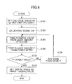
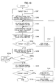
- FIG. 4 is a flowchart illustrating a control procedure for determining a target digital value with the circuit configuration in FIG. 3 .
- the CPU 1 sets a DAC code to a value corresponding to the LD 6 not emitting light (Step S101) with the LD lighting signal turned on (Step S102).
- a digital value is taken in from the PD 7 based on a light-emitting amount of the LD 6 (Step S103), and an optical amount P is taken in from the power meter 13 (Step S104).
- the procedure of Steps S103 to S105 is repeated, incrementing by 1 the DAC code until P becomes the target value (Steps 105, 106).
- the digital value based on the DAC code at that time becomes the target digital value (Step 107).
- the control procedure as described above, which is programmed, is executed at the CPU 1.
- the CPU 1 keeps the target digital value determined in Step S107, and thereafter uses the target digital value to keep the light amount of the LD 6 at a constant value.
- Controlling in this way allows doing away with a hold capacitor as the setting value of the LD drive current is set in the DAC 2.
- FIG. 5 is a flowchart illustrating another control procedure for determining the target digital value with the circuit configuration in FIG. 3 .
- the decision as to whether the light amount P in Step S105 is the target value is changed to a decision as to whether it is greater than the target value, and the process of making the increment of the DAC code of step S106 to be 1 is changed to the process of making the increment of the DAC code of step S106 to be m.
- Step S105a - No With the control procedure in FIG. 5 , with the light amount not reaching the target (Step S105a - No), the DAC code is incremented by a step m which is larger than the minimum resolution of the DAC. Then, when the light amount reaches an amount not less than the target, the target digital value is calculated from the digital value from the PD 7, the light amount, and the target light amount as shown in equation (1) (Step S107a). In this way, a target digital value can be accurately determined even if the light amount does not match the target. Moreover, increasing the DAC code in an increment larger than a minimum resolution of the DAC makes it possible to reduce the time required for the control process. Each of the other steps is processed in a similar manner to that of FIG. 3 .
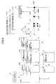
- FIG. 6 is a block diagram illustrating a circuit configuration of a light amount control apparatus according to a second embodiment of the invention. While the first embodiment is directed to an arrangement with a single light-emitting point (light-emitting source), the second embodiment here is directed to an arrangement with N light-emitting points (where N is a positive integer no less than 2).
- N DACs 2, N V/I converters 3, N current amplifiers 4, N switching elements 5, and N LDs 6 are provided. As shown, the respective elements 1 to N are marked _1, _2, ..., _N.
- the CPU 1 sets a DAC code 1 corresponding to a LD drive current in a DAC_1 (2_1).
- the DAC_1 (2_1) outputs a voltage according to the set DAC code 1.
- the voltage output from the DAC_1 (2_1) is converted at the V/I converter_1 (3_1) to a current, which is input to the current amplifier_1 (4_1).
- the output current from the current amplifier_1 (4_1) is supplied to LD_1 (6_1), which turns on at a light amount according to the current.
- the light output from the LD_1 (6_1) is divided with a half mirror 14 into two beams, one of which is input to the PD (photodetector) 7, while the other is directed to the recording medium 12.
- the beam input to the PD 7 is converted to a current, which, at the I/V converter 8 is converted to a voltage, which is input to the ADC 9.
- the converted digital output of the ADC 9 is input to the CPU 1.
- the CPU 1 compares the converted digital input from the ADC 9 with the predetermined target digital value_1, and computes a new DAC code_1 such that the converted digital input and the target digital value_1 match. Thereafter, the CPU 1 sets the new DAC code_1 in the DAC 2.
- the control process as described above is sequentially performed for LD_2...N, which repeating allows keeping the respective LD 6 output light amounts at a predetermined target value.
- FIG. 7 is a timing chart illustrating timings of controlling the light amount while outputting an image.
- the illustrated timing chart shows output timings of a sync detect signal, an image output period, a sample-and-hold (S/H) signal, LD lighting signals 1 through 4, an ADC sampling signal, setting-value compute signals 1 through 4, and DAC setting signals 1 through 4.
- the sync detect signal which is for setting a write-start timing when starting optical writing and for synchronizing the subsequent timing, is obtained by detecting a scanned light with a sync detect sensor. A predetermined time after the sync detect signal is turned on, an image output period starts and the LD_1 to 4 (6_1 to 4) turns on.
- inputting a sample-and-hold signal 10 leads to an ADC sampling signal output, according to which the setting value of the DAC_1 to 4 (2_1 to 4) is computed and the respective DAC_1 to 4 (2_1 to 4) codes are set.
- FIG. 8 is a block diagram illustrating a circuit configuration for determining a target digital value according to the second embodiment.
- FIG. 8 shows the arrangement in FIG. 6 additionally provided with just an optical power meter 13.
- FIG. 9 is a flowchart illustrating a control procedure for determining a target digital value with the circuit configuration in FIG. 8 .
- the control target is set to Channel 1 (Step S201) to start the procedure from a "_1" circuit.
- the CPU 1 sets a DAC code to a value corresponding to the LD_1 (6_1) not emitting light (Step S202) with the LD lighting signal of the target channel turned on (Step S203).
- a digital value is taken in from PD_1 (7_1) based on a light-emitting amount of LD_1 (6_1) (Step S204), and an optical amount P is taken in from the power meter 13 (Step S205).
- Steps S202 through S206 are repeated, incrementing the DAC code until P becomes the target value (Steps 206, 207).
- the digital value based on the DAC code at that time becomes the target digital value (Step 208).
- the LD lighting signal of the target channel is turned off (Step S209), and procedures of Steps S202 through S211 are repeated until the target channel becomes N (Steps 210, 211) to determine the target digital value for Channels 1 to N.
- the procedure ends once the target digital values are determined for all the Channels.
- the flowchart for the above procedure, which is programmed, is executed at the CPU 1.
- the multiple target digital values determined with the control procedure as shown in FIG. 9 are kept in the CPU 1, and thereafter, the multiple target digital values are used to keep the respective LD light amounts at a constant value.
- Controlling in this way allows doing away with a hold capacitor as the setting values of the LD drive currents are set equal to the corresponding DAC_1-N (2_1-N).
- This embodiment may be arranged such that, while the CPU 1 is operating with the procedure in FIG. 8 to determine a target digital value, the control procedure is embodied with an adjusting step and the determined target digital value is stored in a CPU 1-associated non-volatile storing device (not shown).
- the target digital value stored in the non-volatile storing device is used to keep the LD light amount at a constant value.
- the control procedure for determining a target digital value makes it unnecessary to execute it at a printing device.
- FIG. 10 is a flowchart illustrating another control procedure for determining the target digital values with the circuit configuration in FIG. 8 .
Landscapes
- Physics & Mathematics (AREA)
- Optics & Photonics (AREA)
- Health & Medical Sciences (AREA)
- General Health & Medical Sciences (AREA)
- Toxicology (AREA)
- Semiconductor Lasers (AREA)
- Laser Beam Printer (AREA)
- Exposure Or Original Feeding In Electrophotography (AREA)
Abstract
Description
- The present invention relates to a light amount control apparatus for a light source used in optical writing, an optical writing apparatus with the light amount control apparatus, and an image forming apparatus with the optical writing apparatus.
- A laser diode is generally used as a writing light source for a printing device such as a printer or copier. The laser diode used as an optical writing light source requires that a light emission amount be kept to a constant value for making the density of a generated image constant. Thus,
JP2001-138566A - Recently, a light-emitting device has also been developed which has a large number of light-emitting points in one package, and is used as a writing light source for a printing device. For example,
JP2003-266774A - However, with the control method as disclosed in
JP2001-138566 JP2003-266774A - Now, a problem to be solved by the present invention is to ensure control sufficient to keep the light amount constant, and to ensure control sufficient to keep the light amount constant even with, especially, a light source with a large number of light-emitting points.
- Accordingly, it is a general object of the present invention to provide techniques for light amount control for a light source used in optical writing, for optical writing with the light amount control, and for image forming with the optical writing apparatus that substantially obviate one or more problems caused by the limitations and disadvantages of the related art.
- According to the invention, a light-amount control apparatus for controlling an output light amount of light sources used for optical writing includes one or more drive units for supplying a drive current to the light source; one or more drive-current setting units for determining an amount of the drive current provided to the light source from the drive unit; a light-amount detecting unit for detecting an output light from the light source, and outputting a voltage according to the detected light amount; and a processing unit for setting the drive current amount based on the detected value detected with the light-amount detecting unit.
- Other objects, features, and advantages of the present invention will become more apparent from the following detailed descriptions when read in conjunction with the accompanying drawings, in which:
-
FIG. 1 is a block diagram illustrating a circuit configuration of a light amount control apparatus according to a first embodiment of the invention; -
FIG. 2 is a timing chart illustrating timings of controlling the light amount while outputting an image, according to the first embodiment of the invention; -
FIG. 3 is a block diagram illustrating a circuit configuration for determining a target digital value according to the first embodiment; -
FIG. 4 is a flowchart illustrating a control procedure for determining a target digital value with the circuit configuration inFIG. 3 ; -
FIG. 5 is a flowchart illustrating another control procedure for determining the target digital value with the circuit configuration inFIG. 3 ; -
FIG. 6 is a block diagram illustrating a circuit configuration of a light amount control apparatus according to a second embodiment of the invention; -
FIG. 7 is a timing chart illustrating timings of controlling the light amount while outputting an image, according to the second embodiment of the invention; -
FIG. 8 is a block diagram illustrating a circuit configuration for determining a target digital value according to the second embodiment; -
FIG. 9 is a flowchart illustrating a control procedure for determining a target digital value with the circuit configuration inFIG. 8 ; and -
FIG. 10 is a flowchart illustrating another control procedure for determining the target digital values with the circuit configuration inFIG. 8 . - Descriptions are given next, with reference to the accompanying drawings, of embodiments of the present invention.
- The present invention is not limited to the specifically disclosed embodiments, but variations and modifications may be made without departing from the scope of the present invention.
- Embodiments according to the present invention are described, referring to
FIG. 1 through FIG. 10 . -
FIG. 1 is a block diagram illustrating a circuit configuration of a light amount control apparatus according to a first embodiment of the invention. As shown, the light amount control apparatus basically includes aCPU 1, a DAC (digital/analog converter) 2, a V/I (voltage/current)converter 3, acurrent amplifier 4, aswitching element 5, a LD (laser diode) 6, a PD (photodiode) 7, an I/V (current/voltage)converter 8, and an ADC (analog/digital converter) 9. - In a light amount control apparatus having the constituting elements as described above, the
CPU 1 sets a DAC code corresponding to a LD drive current in theDAC 2 based on a sample-and-hold signal 10 input from a sample-and-hold circuit (not shown). TheDAC 2 outputs a voltage according to the set DAC code. The voltage output from theDAC 2 is converted at the V/I converter 3 to a current, which is input to thecurrent amplifier 4. With aLD lighting signal 11 on, a current output from thecurrent amplifier 4 is supplied to theLD 6, which turns on at a light amount according to the current. - A light output from the
LD 6 is divided with ahalf mirror 14 into two beams, one of which is input to thePD 7 as a photodetector. The other is directed to arecording medium 12 of the image forming apparatus body. The beam input to thePD 7 is converted to a current, which, at the I/V converter 8, is converted to a voltage, which is input to theADC 9. The converted digital output of theADC 9 is input to theCPU 1. TheCPU 1 compares the converted digital value input from theADC 9 with a predetermined target digital value, and computes a new DAC code such that the converted digital input and the target digital value match. Thereafter, theCPU 1 sets a new DAC code in theDAC 2. - Executing such a series of control loops as described above allows keeping an output light amount of the
LD 6 at the predetermined target value. -
FIG. 2 is a timing chart illustrating timings of controlling the light amount while outputting an image. The timing chart shows output timings of a sync detect signal, an image output period, a LD lighting signal, a sample-and-hold (S/H) signal, an ADC sampling signal, a setting-value compute signal, and a DAC setting signal. The sync detect signal, which is for setting a write-start timing when starting optical writing, and for synchronizing the subsequent timing, is obtained by detecting a scanned light with a sync detect sensor. A predetermined time after the sync detect signal is turned on, an image output period starts and theLD 6 turns on. Moreover, inputting a sample-and-hold signal 10 leads to an ADC sampling signal output, according to which the setting value of theDAC 2 is computed and the DAC code set. -
FIG. 3 is a block diagram illustrating a circuit configuration for determining a target digital value. The control process here requires determining in advance the target digital value in order to keep the light amount of theLD 6 at a target value. Now, as illustrated inFIG. 3 , in order to determine a target digital value with the light amount of theLD 6 being the target value, within a light path to therecording medium 12 is inserted anoptical power meter 13 for measuring a physical amount of the LD light amount, an output of which meter is input to theCPU 1. Here, measuring a physical amount means obtaining an absolute value of a light amount. -
FIG. 4 is a flowchart illustrating a control procedure for determining a target digital value with the circuit configuration inFIG. 3 . With the control procedure, theCPU 1 sets a DAC code to a value corresponding to theLD 6 not emitting light (Step S101) with the LD lighting signal turned on (Step S102). Then, a digital value is taken in from thePD 7 based on a light-emitting amount of the LD 6 (Step S103), and an optical amount P is taken in from the power meter 13 (Step S104). Then, the procedure of Steps S103 to S105 is repeated, incrementing by 1 the DAC code until P becomes the target value (Steps 105, 106). When the light amount P becomes the target value, the digital value based on the DAC code at that time becomes the target digital value (Step 107). The control procedure as described above, which is programmed, is executed at theCPU 1. - In this way, the
CPU 1 keeps the target digital value determined in Step S107, and thereafter uses the target digital value to keep the light amount of theLD 6 at a constant value. - Controlling in this way allows doing away with a hold capacitor as the setting value of the LD drive current is set in the
DAC 2. -
FIG. 5 is a flowchart illustrating another control procedure for determining the target digital value with the circuit configuration inFIG. 3 . With this control procedure, the decision as to whether the light amount P in Step S105 is the target value is changed to a decision as to whether it is greater than the target value, and the process of making the increment of the DAC code of step S106 to be 1 is changed to the process of making the increment of the DAC code of step S106 to be m. Moreover, with the changes as described above, the process of computing the target digital value in Step S107 is changed to the process in step S107 of:
- In other words, with the control procedure in
FIG. 5 , with the light amount not reaching the target (Step S105a - No), the DAC code is incremented by a step m which is larger than the minimum resolution of the DAC. Then, when the light amount reaches an amount not less than the target, the target digital value is calculated from the digital value from thePD 7, the light amount, and the target light amount as shown in equation (1) (Step S107a). In this way, a target digital value can be accurately determined even if the light amount does not match the target. Moreover, increasing the DAC code in an increment larger than a minimum resolution of the DAC makes it possible to reduce the time required for the control process. Each of the other steps is processed in a similar manner to that ofFIG. 3 . - The control procedure as described above, which is programmed, is executed at the
CPU 1. -
FIG. 6 is a block diagram illustrating a circuit configuration of a light amount control apparatus according to a second embodiment of the invention. While the first embodiment is directed to an arrangement with a single light-emitting point (light-emitting source), the second embodiment here is directed to an arrangement with N light-emitting points (where N is a positive integer no less than 2). - Thus, in this embodiment, compared to the light amount control apparatus in the first embodiment,
N DACs 2, N V/I converters 3, Ncurrent amplifiers 4,N switching elements 5, andN LDs 6 are provided. As shown, therespective elements 1 to N are marked _1, _2, ..., _N. - In the light amount control apparatus thus arranged, the
CPU 1 sets aDAC code 1 corresponding to a LD drive current in a DAC_1 (2_1). The DAC_1 (2_1) outputs a voltage according to theset DAC code 1. The voltage output from the DAC_1 (2_1) is converted at the V/I converter_1 (3_1) to a current, which is input to the current amplifier_1 (4_1). When the LD lighting signal_1 (11_1) is on, the output current from the current amplifier_1 (4_1) is supplied to LD_1 (6_1), which turns on at a light amount according to the current. - The light output from the LD_1 (6_1) is divided with a
half mirror 14 into two beams, one of which is input to the PD (photodetector) 7, while the other is directed to therecording medium 12. The beam input to thePD 7 is converted to a current, which, at the I/V converter 8 is converted to a voltage, which is input to theADC 9. The converted digital output of theADC 9 is input to theCPU 1. - The
CPU 1 compares the converted digital input from theADC 9 with the predetermined target digital value_1, and computes a new DAC code_1 such that the converted digital input and the target digital value_1 match. Thereafter, theCPU 1 sets the new DAC code_1 in theDAC 2. - The control process as described above is sequentially performed for LD_2...N, which repeating allows keeping the
respective LD 6 output light amounts at a predetermined target value. -
FIG. 7 is a timing chart illustrating timings of controlling the light amount while outputting an image. In this example, for N=4, light amounts of two LDs are controlled within one scan period. - The illustrated timing chart shows output timings of a sync detect signal, an image output period, a sample-and-hold (S/H) signal, LD lighting signals 1 through 4, an ADC sampling signal, setting-value compute signals 1 through 4, and DAC setting signals 1 through 4. The sync detect signal, which is for setting a write-start timing when starting optical writing and for synchronizing the subsequent timing, is obtained by detecting a scanned light with a sync detect sensor. A predetermined time after the sync detect signal is turned on, an image output period starts and the LD_1 to 4 (6_1 to 4) turns on. Moreover, inputting a sample-and-
hold signal 10 leads to an ADC sampling signal output, according to which the setting value of the DAC_1 to 4 (2_1 to 4) is computed and the respective DAC_1 to 4 (2_1 to 4) codes are set. - Again the control process here requires individually determining in advance the target digital value in order to keep the light amount of the respective LD_1 to 4 (6_1 to 4) at a target value. Now in this embodiment, as in the first embodiment, in order to determine a target digital value with the light amount of the respective LDs being the target value, within a light path to the recording medium is inserted an
optical power meter 13 for measuring a physical amount of the LD light amount, an output of which meter is input to theCPU 1.FIG. 8 is a block diagram illustrating a circuit configuration for determining a target digital value according to the second embodiment.FIG. 8 shows the arrangement inFIG. 6 additionally provided with just anoptical power meter 13. Thus, the identical elements are assigned the identical reference letters, so that duplicating explanations are omitted. -
FIG. 9 is a flowchart illustrating a control procedure for determining a target digital value with the circuit configuration inFIG. 8 . With this control procedure, first the control target is set to Channel 1 (Step S201) to start the procedure from a "_1" circuit. Now, theCPU 1 sets a DAC code to a value corresponding to the LD_1 (6_1) not emitting light (Step S202) with the LD lighting signal of the target channel turned on (Step S203). Then, a digital value is taken in from PD_1 (7_1) based on a light-emitting amount of LD_1 (6_1) (Step S204), and an optical amount P is taken in from the power meter 13 (Step S205). Then, the procedures of Steps S202 through S206 are repeated, incrementing the DAC code until P becomes the target value (Steps 206, 207). When the light amount P becomes the target value, the digital value based on the DAC code at that time becomes the target digital value (Step 208). Then, the LD lighting signal of the target channel is turned off (Step S209), and procedures of Steps S202 through S211 are repeated until the target channel becomes N (Steps 210, 211) to determine the target digital value forChannels 1 to N. The procedure ends once the target digital values are determined for all the Channels. The flowchart for the above procedure, which is programmed, is executed at theCPU 1. - The multiple target digital values determined with the control procedure as shown in
FIG. 9 are kept in theCPU 1, and thereafter, the multiple target digital values are used to keep the respective LD light amounts at a constant value. - Controlling in this way allows doing away with a hold capacitor as the setting values of the LD drive currents are set equal to the corresponding DAC_1-N (2_1-N).
- This embodiment may be arranged such that, while the
CPU 1 is operating with the procedure inFIG. 8 to determine a target digital value, the control procedure is embodied with an adjusting step and the determined target digital value is stored in a CPU 1-associated non-volatile storing device (not shown). When operating as a printing device, the target digital value stored in the non-volatile storing device is used to keep the LD light amount at a constant value. Here, the control procedure for determining a target digital value makes it unnecessary to execute it at a printing device. -
FIG. 10 is a flowchart illustrating another control procedure for determining the target digital values with the circuit configuration inFIG. 8 . With this control procedure, for determining the target digital values for the second and subsequent LD_2...N (6_2...N), as an initial value for the DAC code, a multiplier less than 1 (the multiplier=0.8 inFIG. 10 ) is multiplied by the DAC code at the time the first LD_1 (6_1) reaches the target value, with the process of Steps S203 and thereafter being executed from theChannel 1 to N based on the resulting value. This makes it possible to reduce the time required for the control process as LD_l...N (6_1...N) would not emit light more than necessary, and the process flow starts from a light amount close to the target light amount. Each of the other steps are processed in a manner similar to that ofFIG. 9 . - Again the control procedure as described above, which is programmed, is executed at the
CPU 1. - The present application is based on the Japanese Priority Application No.
2007-054312 filed on March 5, 2007
Claims (13)
- A light-amount control apparatus for controlling an output light amount of one or more light sources used for optical writing, comprising:a drive unit for supplying a drive current to the light source;a drive-current setting unit for determining an amount of the drive current supplied to the light source from the drive unit;a light-amount detecting unit for detecting an output light from the light source, and outputting a voltage according to the detected light amount; anda processing unit for setting the drive current amount based on the detected value detected with the light-amount detecting unit.
- The light-amount control apparatus as claimed in claim 1, further comprising an A/D conversion unit, wherein the A/D conversion unit A/D converts the detected value of the light amount detected as the voltage with the light-amount detecting unit,
and the processing unit sets the drive current amount based on the voltage value A/D converted with the A/D conversion unit. - The light-amount control apparatus as claimed in claim 2, wherein
there are multiple numbers of the drive units and the drive-current setting units. - The light-amount control apparatus as claimed in claim 2, further comprising:a light-amount measuring unit for measuring a physical amount of the light amount output from the light source, whereinthe processing unit progressively increments the drive current amount from a value at which the light source does not emit light, and sets the drive current amount with the converted value at the A/D conversion unit at a time the physical amount measured with the light-amount measuring unit becomes a target value.
- The light-amount control apparatus as claimed in claim 2, further comprising:a light-amount measuring unit for measuring a physical amount of the light amount output from the light source, whereinthe processing unit progressively increments the drive current amount from a value at which the light source does not emit light, and computes a subsequent target value from the converted value at the A/D conversion unit at a time the physical amount measured with the light-amount measuring unit approaches a physical amount near a target value and from the physical amount near the target value to set the drive current amount as the subsequent target value.
- The light-amount control apparatus as claimed in claim 3, further comprising a light-amount measuring unit for measuring a physical amount of the light amount output from the light source, wherein
the processing unit progressively increments the drive current amount for the respective light sources from a value at which the light source does not emit light, and sets the drive current amount of the respective light sources with the converted value at the A/D conversion unit at a time the physical amount measured with the light-amount measuring unit becomes a target value as a subsequent target value. - The light-amount control apparatus as claimed in claim 3, further comprising a light-amount measuring unit for measuring a physical amount of the light amount output from the light source, wherein
the processing unit repeats the steps of:progressively incrementing the drive current amount for a first light source from a value at which the light source does not emit light, setting the drive current amount of the light source with the converted value at the A/D conversion unit at a time the physical amount measured with the light-amount measuring unit becomes a target value as a subsequent target value, keeping the set drive current amount, and, for a second light source and subsequent light sources, progressively incrementing from a value multiplied by a predetermined multiplier to a value of the kept drive current amount kept at the drive current amount supplied to the light sources, and setting the drive current amount. - The light-amount control apparatus as claimed in claim 3, further comprising a light-amount measuring unit for measuring a physical amount of the light amount output from the light source, wherein
the processing unit progressively increments the drive current amount for the respective light sources from a value at which the light source does not emit light, and sets the drive current amount of the respective light sources with a value computed from the converted value at the A/D conversion unit at a time the physical amount measured with the light-amount measuring unit approaches a physical amount near the target value and from the physical amount near the target value as a subsequent target value. - The light-amount control apparatus as claimed in claim 8, wherein an equation for calculating a subsequent target value from an A/D converted value of the detected value of the light amount at a time the physical amount of the light amount becomes a value near the target value, and the physical amount of the light amount is:a target A/D converted value of the detected value of the light amount = (the physical amount of the target light amount / the physical amount of the measured light amount) x (the A/D converted value of the detected value of the current light amount).
- The light-amount control apparatus as claimed in claim 8, wherein
the processing unit includes a storing unit for storing the target value. - The light-amount control apparatus as claimed in claim 10, wherein
the light source is a laser diode. - An optical writing apparatus, comprising:the light-amount control apparatus as claimed in claim 1.
- An image forming apparatus, comprising:the light-amount control apparatus as claimed in claim 12.
Applications Claiming Priority (1)
| Application Number | Priority Date | Filing Date | Title |
|---|---|---|---|
| JP2007054312A JP2008218720A (en) | 2007-03-05 | 2007-03-05 | Light amount control device, optical writing device, and image forming device |
Publications (2)
| Publication Number | Publication Date |
|---|---|
| EP1967371A1 true EP1967371A1 (en) | 2008-09-10 |
| EP1967371B1 EP1967371B1 (en) | 2010-05-12 |
Family
ID=39383988
Family Applications (1)
| Application Number | Title | Priority Date | Filing Date |
|---|---|---|---|
| EP08152256A Ceased EP1967371B1 (en) | 2007-03-05 | 2008-03-04 | Light amount control, optical writing, and image forming apparatuses |
Country Status (4)
| Country | Link |
|---|---|
| US (1) | US8076626B2 (en) |
| EP (1) | EP1967371B1 (en) |
| JP (1) | JP2008218720A (en) |
| DE (1) | DE602008001177D1 (en) |
Families Citing this family (3)
| Publication number | Priority date | Publication date | Assignee | Title |
|---|---|---|---|---|
| US8022347B2 (en) * | 2008-06-23 | 2011-09-20 | Ricoh Company, Ltd. | Optical scanning device, image forming apparatus, and optical scanning method having a plurality of light intensity control devices with a switching unit |
| JP5446635B2 (en) | 2008-09-16 | 2014-03-19 | 株式会社リコー | Image forming apparatus and image forming method |
| JP5728862B2 (en) | 2010-09-16 | 2015-06-03 | 株式会社リコー | Optical device, optical device control method, and image forming apparatus |
Citations (6)
| Publication number | Priority date | Publication date | Assignee | Title |
|---|---|---|---|---|
| JPS62124576A (en) | 1985-11-26 | 1987-06-05 | Ricoh Co Ltd | Semiconductor laser output adjustment device |
| EP0258060A2 (en) | 1986-08-27 | 1988-03-02 | Canon Kabushiki Kaisha | Light quantity control device |
| JPH02151455A (en) | 1988-12-02 | 1990-06-11 | Ricoh Co Ltd | Semiconductor laser light intensity modulation circuit |
| US5965868A (en) | 1996-04-16 | 1999-10-12 | Canon Kabushiki Kaisha | Laser light quantity control device |
| US20040145546A1 (en) | 2002-11-21 | 2004-07-29 | Fuji Photo Film Co., Ltd. | Exposure apparatus |
| EP1528501A1 (en) | 2003-10-29 | 2005-05-04 | Ricoh Company, Ltd. | Method and apparatus for optical writing capable of writing a wide format image using a plurality of light emitting devices |
Family Cites Families (5)
| Publication number | Priority date | Publication date | Assignee | Title |
|---|---|---|---|---|
| JPS6190540A (en) * | 1984-10-09 | 1986-05-08 | Olympus Optical Co Ltd | Optical output stabilizer |
| JP3567645B2 (en) * | 1996-08-12 | 2004-09-22 | 富士ゼロックス株式会社 | Image recording device |
| JP2001138566A (en) | 1999-11-12 | 2001-05-22 | Ricoh Co Ltd | Image forming device |
| JP4045822B2 (en) | 2002-03-19 | 2008-02-13 | 富士ゼロックス株式会社 | Image forming apparatus |
| JP3695413B2 (en) * | 2002-03-29 | 2005-09-14 | ソニー株式会社 | Light emitting element driving apparatus and image forming apparatus |
-
2007
- 2007-03-05 JP JP2007054312A patent/JP2008218720A/en active Pending
-
2008
- 2008-02-29 US US12/039,955 patent/US8076626B2/en not_active Expired - Fee Related
- 2008-03-04 EP EP08152256A patent/EP1967371B1/en not_active Ceased
- 2008-03-04 DE DE602008001177T patent/DE602008001177D1/en active Active
Patent Citations (6)
| Publication number | Priority date | Publication date | Assignee | Title |
|---|---|---|---|---|
| JPS62124576A (en) | 1985-11-26 | 1987-06-05 | Ricoh Co Ltd | Semiconductor laser output adjustment device |
| EP0258060A2 (en) | 1986-08-27 | 1988-03-02 | Canon Kabushiki Kaisha | Light quantity control device |
| JPH02151455A (en) | 1988-12-02 | 1990-06-11 | Ricoh Co Ltd | Semiconductor laser light intensity modulation circuit |
| US5965868A (en) | 1996-04-16 | 1999-10-12 | Canon Kabushiki Kaisha | Laser light quantity control device |
| US20040145546A1 (en) | 2002-11-21 | 2004-07-29 | Fuji Photo Film Co., Ltd. | Exposure apparatus |
| EP1528501A1 (en) | 2003-10-29 | 2005-05-04 | Ricoh Company, Ltd. | Method and apparatus for optical writing capable of writing a wide format image using a plurality of light emitting devices |
Also Published As
| Publication number | Publication date |
|---|---|
| DE602008001177D1 (en) | 2010-06-24 |
| EP1967371B1 (en) | 2010-05-12 |
| US20080218723A1 (en) | 2008-09-11 |
| US8076626B2 (en) | 2011-12-13 |
| JP2008218720A (en) | 2008-09-18 |
Similar Documents
| Publication | Publication Date | Title |
|---|---|---|
| EP1821512B1 (en) | Exposure apparatus | |
| EP2602668A2 (en) | Optical scanning apparatus and image forming apparatus | |
| EP2785037B1 (en) | Image reading device, image forming apparatus, and image reading method | |
| EP3133446A1 (en) | Image forming apparatus | |
| US8957932B2 (en) | Exposure apparatus and image forming apparatus | |
| US8076626B2 (en) | Light amount control, optical writing, and image forming apparatuses having a plurality of drive-current setting units | |
| US7852363B2 (en) | Light scanning apparatus, image forming apparatus, and light power control method | |
| US9225867B2 (en) | Image reading apparatus | |
| US9500980B2 (en) | Image forming apparatus of electrophotographic system | |
| JP2011187494A (en) | Semiconductor laser-driving device and image forming device equipped with the same | |
| JPH05212900A (en) | Image forming method | |
| US9185256B2 (en) | Image reading device, image forming apparatus, and non-transitory computer readable medium storing image reading program | |
| US7406110B2 (en) | Method and apparatus for controlling power of laser diodes | |
| US8933979B2 (en) | Electrophotographic-type image forming apparatus | |
| US8289356B2 (en) | Light output device and image forming apparatus including the same | |
| JP2009023145A (en) | Image formation device and exposure device | |
| JPH05212892A (en) | Recording density correction device | |
| US20050083978A1 (en) | Method for controlling laser beam power balance in laser scanning unit | |
| JP5667746B2 (en) | Image forming apparatus | |
| US6714231B2 (en) | Image forming apparatus and laser drive control method therein | |
| JP5848598B2 (en) | Optical scanning apparatus and image forming apparatus | |
| JP2002190641A (en) | Image forming device | |
| JP2010165981A (en) | Semiconductor laser driving device and light scanning device with the same, and image forming apparatus | |
| JP5219405B2 (en) | Correction value determination device, correction value determination method, and optical scanning device | |
| JP5707759B2 (en) | Light quantity control device, optical scanning device, and image forming apparatus |
Legal Events
| Date | Code | Title | Description |
|---|---|---|---|
| PUAI | Public reference made under article 153(3) epc to a published international application that has entered the european phase |
Free format text: ORIGINAL CODE: 0009012 |
|
| AK | Designated contracting states |
Kind code of ref document: A1 Designated state(s): AT BE BG CH CY CZ DE DK EE ES FI FR GB GR HR HU IE IS IT LI LT LU LV MC MT NL NO PL PT RO SE SI SK TR |
|
| AX | Request for extension of the european patent |
Extension state: AL BA MK RS |
|
| 17P | Request for examination filed |
Effective date: 20090109 |
|
| AKX | Designation fees paid |
Designated state(s): DE ES FR GB IT NL |
|
| GRAP | Despatch of communication of intention to grant a patent |
Free format text: ORIGINAL CODE: EPIDOSNIGR1 |
|
| GRAS | Grant fee paid |
Free format text: ORIGINAL CODE: EPIDOSNIGR3 |
|
| GRAA | (expected) grant |
Free format text: ORIGINAL CODE: 0009210 |
|
| AK | Designated contracting states |
Kind code of ref document: B1 Designated state(s): DE ES FR GB IT NL |
|
| REG | Reference to a national code |
Ref country code: GB Ref legal event code: FG4D |
|
| REF | Corresponds to: |
Ref document number: 602008001177 Country of ref document: DE Date of ref document: 20100624 Kind code of ref document: P |
|
| REG | Reference to a national code |
Ref country code: NL Ref legal event code: VDEP Effective date: 20100512 |
|
| PG25 | Lapsed in a contracting state [announced via postgrant information from national office to epo] |
Ref country code: ES Free format text: LAPSE BECAUSE OF FAILURE TO SUBMIT A TRANSLATION OF THE DESCRIPTION OR TO PAY THE FEE WITHIN THE PRESCRIBED TIME-LIMIT Effective date: 20100823 Ref country code: NL Free format text: LAPSE BECAUSE OF FAILURE TO SUBMIT A TRANSLATION OF THE DESCRIPTION OR TO PAY THE FEE WITHIN THE PRESCRIBED TIME-LIMIT Effective date: 20100512 |
|
| PLBE | No opposition filed within time limit |
Free format text: ORIGINAL CODE: 0009261 |
|
| STAA | Information on the status of an ep patent application or granted ep patent |
Free format text: STATUS: NO OPPOSITION FILED WITHIN TIME LIMIT |
|
| PG25 | Lapsed in a contracting state [announced via postgrant information from national office to epo] |
Ref country code: IT Free format text: LAPSE BECAUSE OF FAILURE TO SUBMIT A TRANSLATION OF THE DESCRIPTION OR TO PAY THE FEE WITHIN THE PRESCRIBED TIME-LIMIT Effective date: 20100512 |
|
| 26N | No opposition filed |
Effective date: 20110215 |
|
| REG | Reference to a national code |
Ref country code: DE Ref legal event code: R097 Ref document number: 602008001177 Country of ref document: DE Effective date: 20110214 |
|
| REG | Reference to a national code |
Ref country code: FR Ref legal event code: PLFP Year of fee payment: 9 |
|
| REG | Reference to a national code |
Ref country code: FR Ref legal event code: PLFP Year of fee payment: 10 |
|
| REG | Reference to a national code |
Ref country code: FR Ref legal event code: PLFP Year of fee payment: 11 |
|
| PGFP | Annual fee paid to national office [announced via postgrant information from national office to epo] |
Ref country code: GB Payment date: 20220321 Year of fee payment: 15 |
|
| PGFP | Annual fee paid to national office [announced via postgrant information from national office to epo] |
Ref country code: FR Payment date: 20220322 Year of fee payment: 15 |
|
| PGFP | Annual fee paid to national office [announced via postgrant information from national office to epo] |
Ref country code: DE Payment date: 20220620 Year of fee payment: 16 |
|
| GBPC | Gb: european patent ceased through non-payment of renewal fee |
Effective date: 20230304 |
|
| PG25 | Lapsed in a contracting state [announced via postgrant information from national office to epo] |
Ref country code: GB Free format text: LAPSE BECAUSE OF NON-PAYMENT OF DUE FEES Effective date: 20230304 |
|
| PG25 | Lapsed in a contracting state [announced via postgrant information from national office to epo] |
Ref country code: GB Free format text: LAPSE BECAUSE OF NON-PAYMENT OF DUE FEES Effective date: 20230304 Ref country code: FR Free format text: LAPSE BECAUSE OF NON-PAYMENT OF DUE FEES Effective date: 20230331 |
|
| REG | Reference to a national code |
Ref country code: DE Ref legal event code: R119 Ref document number: 602008001177 Country of ref document: DE |
|
| PG25 | Lapsed in a contracting state [announced via postgrant information from national office to epo] |
Ref country code: DE Free format text: LAPSE BECAUSE OF NON-PAYMENT OF DUE FEES Effective date: 20241001 |
|
| PG25 | Lapsed in a contracting state [announced via postgrant information from national office to epo] |
Ref country code: DE Free format text: LAPSE BECAUSE OF NON-PAYMENT OF DUE FEES Effective date: 20241001 |