EP1965420A2 - Compliant pin strip with integrated dam bar - Google Patents
Compliant pin strip with integrated dam bar Download PDFInfo
- Publication number
- EP1965420A2 EP1965420A2 EP08151654A EP08151654A EP1965420A2 EP 1965420 A2 EP1965420 A2 EP 1965420A2 EP 08151654 A EP08151654 A EP 08151654A EP 08151654 A EP08151654 A EP 08151654A EP 1965420 A2 EP1965420 A2 EP 1965420A2
- Authority
- EP
- European Patent Office
- Prior art keywords
- compliant
- pins
- circuit board
- printed circuit
- pin
- Prior art date
- Legal status (The legal status is an assumption and is not a legal conclusion. Google has not performed a legal analysis and makes no representation as to the accuracy of the status listed.)
- Withdrawn
Links
Images
Classifications
-
- B—PERFORMING OPERATIONS; TRANSPORTING
- B29—WORKING OF PLASTICS; WORKING OF SUBSTANCES IN A PLASTIC STATE IN GENERAL
- B29C—SHAPING OR JOINING OF PLASTICS; SHAPING OF MATERIAL IN A PLASTIC STATE, NOT OTHERWISE PROVIDED FOR; AFTER-TREATMENT OF THE SHAPED PRODUCTS, e.g. REPAIRING
- B29C45/00—Injection moulding, i.e. forcing the required volume of moulding material through a nozzle into a closed mould; Apparatus therefor
- B29C45/14—Injection moulding, i.e. forcing the required volume of moulding material through a nozzle into a closed mould; Apparatus therefor incorporating preformed parts or layers, e.g. injection moulding around inserts or for coating articles
- B29C45/14639—Injection moulding, i.e. forcing the required volume of moulding material through a nozzle into a closed mould; Apparatus therefor incorporating preformed parts or layers, e.g. injection moulding around inserts or for coating articles for obtaining an insulating effect, e.g. for electrical components
-
- B—PERFORMING OPERATIONS; TRANSPORTING
- B29—WORKING OF PLASTICS; WORKING OF SUBSTANCES IN A PLASTIC STATE IN GENERAL
- B29C—SHAPING OR JOINING OF PLASTICS; SHAPING OF MATERIAL IN A PLASTIC STATE, NOT OTHERWISE PROVIDED FOR; AFTER-TREATMENT OF THE SHAPED PRODUCTS, e.g. REPAIRING
- B29C45/00—Injection moulding, i.e. forcing the required volume of moulding material through a nozzle into a closed mould; Apparatus therefor
- B29C45/14—Injection moulding, i.e. forcing the required volume of moulding material through a nozzle into a closed mould; Apparatus therefor incorporating preformed parts or layers, e.g. injection moulding around inserts or for coating articles
- B29C45/14336—Coating a portion of the article, e.g. the edge of the article
- B29C45/14418—Sealing means between mould and article
-
- H—ELECTRICITY
- H10—SEMICONDUCTOR DEVICES; ELECTRIC SOLID-STATE DEVICES NOT OTHERWISE PROVIDED FOR
- H10W—GENERIC PACKAGES, INTERCONNECTIONS, CONNECTORS OR OTHER CONSTRUCTIONAL DETAILS OF DEVICES COVERED BY CLASS H10
- H10W74/00—Encapsulations, e.g. protective coatings
- H10W74/01—Manufacture or treatment
Definitions
- This invention relates to the field of electrical packages and more particularly to electrical packages utilizing compliant pin connectors.
- Encased electronic packages with a plurality of pin connectors have typically been prepared by utilizing wave soldering to physically and electrically attach a plurality of pin connectors to a printed circuit board.
- wave soldering has been favored primarily due to the resulting superior mechanical strength of the attachment and the low process costs associated with wave soldering.
- pin-in-paste techniques may be used for electrically and mechanically attaching pin connectors to a printed circuit board. This technique involves applying solder paste to a through hole in the printed circuit board, inserting a connector pin into the solder paste, and then using a reflow soldering technique to achieve a mechanically and electrically robust attachment of the connector pin to the through hole.
- the invention provides an improved technique for fabricating an electrical package having a printed circuit board encased in a housing and pin connectors mechanically and electrically connected to the printed circuit board and extending outwardly away from an outer surface of the housing.
- the process involves first providing a compliant pin strip comprising a plurality of compliant pins that are held together in a spaced apart relationship. At one end of each of the pins there is a compliant portion used for achieving a compliant pin or press-fit connection with a corresponding compliant pin receiving hole in a printed circuit board.
- a dam bar comprises aligned members that extend between adjacent pins transversely of the length direction of the pins. The dam bar and pins together define surfaces for a molding tool to close on and seal a mold cavity during a molding step.
- the compliant portion of each of the plurality of compliant pins is inserted into a corresponding compliant pin receiving hole in a printed circuit board to attach the compliant pin strip to the printed circuit board and thereby make an electrical connection between the printed circuit board and each of the compliant pins.
- the printed circuit board with the attached compliant pin strip is then positioned in a molding tool, and the molding tool is closed so that the printed circuit board is contained within a mold cavity defined by the closed molding tool, and so that molding tool surfaces close on surfaces of the dam bar and pins to seal around the dam bar during a molding step.
- a moldable plastic material is then introduced into the mold cavity. The moldable plastic material is allowed to solidify and form an enclosure for the printed circuit board assembly with a portion of each of the compliant pins projecting outwardly away from a surface of the housing.
- FIG. 1 Shown in FIG. 1 is a compliant pin strip 10 with an integrated dam bar 16.
- the strip 10 comprises a plurality of generally parallel spaced apart electrically conductive compliant pins having a conventional compliant pin portion 12 for achieving a compliant pin or press-fit connection with a through-hole in a printed circuit board 20 that mechanically and electrically joins each of pins 17 to the printed circuit board ( FIG. 3 ).
- Dam bar 16 comprises a plurality of strip-like members that extend between adjacent pins 17 transversely of the length direction of pins 17. In the illustrated embodiment, dam bar 16 is located approximately midway between the ends of the pins.
- dam bar does not interfere with interconnection of the compliant portion 12 with a corresponding compliant pin receiving hole in the printed circuit board, and provided that it is located sufficiently from the end opposite the compliant portion 12 to allow portions of the pins to project outwardly away from a surface of a housing as shown in FIGS. 4 and 5 .
- Pressure tabs 14 may optionally be provided adjacent the compliant portions 12 to provide bearing surfaces for applying pressure to insert the compliant portions 12 into the corresponding receiving holes provided in a printed circuit board.
- a pin tie-down strip 18 may be provided to connect the ends of the pins opposite the compliant portion ends 12 of the pins, such as to maintain a generally parallel spaced apart relationship of the pins during a shaping operation of the compliant pin strip 10, if necessary.
- Compliant pin strip 10 is made of an electrically conductive material (e.g., a metal) and may be formed by using a stamping technique.
- an electrically conductive material e.g., a metal
- pin strip 10 may be shaped or bent in a tool so that the portions of the pins projecting from housing 25 extend at a right angle to the portions of the pins that are inserted into the circuit board 20.
- the printed circuit board and attached strip 10 is inserted into a mold cavity of a molding tool, and the molding tool is closed around the dam bar so that surfaces of the molding tool mate with surfaces of the dam bar to seal the mold cavity.
- a moldable plastic material is injected into the mold cavity.
- Suitable moldable plastic materials include molten thermoplastics and curable thermosetting compositions.
- a housing encasing the printed circuit board 20 is made by cooling the moldable plastic material and thereby solidifying the housing 25.
- curing or cross-linking may be heat initiated or initiated in another suitable manner to cause the liquid thermosetting material to solidify and form housing 25.
- FIG. 5 A substantially completed connector package having a circuit board 20 encased in a housing 25 with pin connectors 17 mechanically and electrically connected to the circuit board and extending outwardly away from an outer surface of housing 25 is shown in FIG. 5 .
- dam bar and pin tie-down strip 10 are sheared away to singulate pins 17.
Landscapes
- Engineering & Computer Science (AREA)
- Manufacturing & Machinery (AREA)
- Mechanical Engineering (AREA)
- Coupling Device And Connection With Printed Circuit (AREA)
- Multi-Conductor Connections (AREA)
Abstract
Description
- This invention relates to the field of electrical packages and more particularly to electrical packages utilizing compliant pin connectors.
- Encased electronic packages with a plurality of pin connectors have typically been prepared by utilizing wave soldering to physically and electrically attach a plurality of pin connectors to a printed circuit board. The use of wave soldering has been favored primarily due to the resulting superior mechanical strength of the attachment and the low process costs associated with wave soldering. Alternatively, pin-in-paste techniques may be used for electrically and mechanically attaching pin connectors to a printed circuit board. This technique involves applying solder paste to a through hole in the printed circuit board, inserting a connector pin into the solder paste, and then using a reflow soldering technique to achieve a mechanically and electrically robust attachment of the connector pin to the through hole. Although these processes have proven satisfactory, improved processes that are less cumbersome and expensive are desirable.
- The invention provides an improved technique for fabricating an electrical package having a printed circuit board encased in a housing and pin connectors mechanically and electrically connected to the printed circuit board and extending outwardly away from an outer surface of the housing. The process involves first providing a compliant pin strip comprising a plurality of compliant pins that are held together in a spaced apart relationship. At one end of each of the pins there is a compliant portion used for achieving a compliant pin or press-fit connection with a corresponding compliant pin receiving hole in a printed circuit board. A dam bar comprises aligned members that extend between adjacent pins transversely of the length direction of the pins. The dam bar and pins together define surfaces for a molding tool to close on and seal a mold cavity during a molding step. In accordance with the invention, the compliant portion of each of the plurality of compliant pins is inserted into a corresponding compliant pin receiving hole in a printed circuit board to attach the compliant pin strip to the printed circuit board and thereby make an electrical connection between the printed circuit board and each of the compliant pins. The printed circuit board with the attached compliant pin strip is then positioned in a molding tool, and the molding tool is closed so that the printed circuit board is contained within a mold cavity defined by the closed molding tool, and so that molding tool surfaces close on surfaces of the dam bar and pins to seal around the dam bar during a molding step. A moldable plastic material is then introduced into the mold cavity. The moldable plastic material is allowed to solidify and form an enclosure for the printed circuit board assembly with a portion of each of the compliant pins projecting outwardly away from a surface of the housing.
- These and other features, advantages and objects of the present invention will be further understood and appreciated by those skilled in the art by reference to the following specification, claims and appended drawings.
- The present invention will now be described, by way of example, with reference to the accompanying drawings, in which:
-
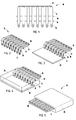
FIG. 1 is a plan view of a compliant pin strip in accordance with the invention. -
FIG. 2 is a perspective view of the compliant pin strip of FIG. after a shaping operation. -
FIG. 3 is a perspective view of the shaped compliant pin strip ofFIG. 2 attached to a printed circuit board. -
FIG. 4 is a perspective view of a finished connector package assembly with the circuit board and compliant pin shown in dashed lines. -
FIG. 5 is a perspective view of the completed connector package assembly. - Shown in
FIG. 1 is acompliant pin strip 10 with an integrateddam bar 16. Thestrip 10 comprises a plurality of generally parallel spaced apart electrically conductive compliant pins having a conventionalcompliant pin portion 12 for achieving a compliant pin or press-fit connection with a through-hole in a printedcircuit board 20 that mechanically and electrically joins each ofpins 17 to the printed circuit board (FIG. 3 ). At the end of eachpin 17 opposite the compliant end portion is a distal end that may be used to connect with an external device.Dam bar 16 comprises a plurality of strip-like members that extend betweenadjacent pins 17 transversely of the length direction ofpins 17. In the illustrated embodiment,dam bar 16 is located approximately midway between the ends of the pins. However, some variation in the location of the dam bar is acceptable, provided that the dam bar does not interfere with interconnection of thecompliant portion 12 with a corresponding compliant pin receiving hole in the printed circuit board, and provided that it is located sufficiently from the end opposite thecompliant portion 12 to allow portions of the pins to project outwardly away from a surface of a housing as shown inFIGS. 4 and 5 . -
Pressure tabs 14 may optionally be provided adjacent thecompliant portions 12 to provide bearing surfaces for applying pressure to insert thecompliant portions 12 into the corresponding receiving holes provided in a printed circuit board. A pin tie-down strip 18 may be provided to connect the ends of the pins opposite thecompliant portion ends 12 of the pins, such as to maintain a generally parallel spaced apart relationship of the pins during a shaping operation of thecompliant pin strip 10, if necessary. -
Compliant pin strip 10 is made of an electrically conductive material (e.g., a metal) and may be formed by using a stamping technique. - As shown in
FIG. 2 ,pin strip 10 may be shaped or bent in a tool so that the portions of the pins projecting fromhousing 25 extend at a right angle to the portions of the pins that are inserted into thecircuit board 20. - After the
compliant portions 12 have been inserted into compliant portion receiving holes defined in printedcircuit board 20, the printed circuit board and attachedstrip 10 is inserted into a mold cavity of a molding tool, and the molding tool is closed around the dam bar so that surfaces of the molding tool mate with surfaces of the dam bar to seal the mold cavity. After the mold is closed, a moldable plastic material is injected into the mold cavity. Suitable moldable plastic materials include molten thermoplastics and curable thermosetting compositions. In the case of thermoplastic materials, a housing encasing the printedcircuit board 20 is made by cooling the moldable plastic material and thereby solidifying thehousing 25. In the case of thermosetting materials, curing or cross-linking may be heat initiated or initiated in another suitable manner to cause the liquid thermosetting material to solidify and formhousing 25. - A substantially completed connector package having a
circuit board 20 encased in ahousing 25 withpin connectors 17 mechanically and electrically connected to the circuit board and extending outwardly away from an outer surface ofhousing 25 is shown inFIG. 5 . - After molding is completed, the dam bar and pin tie-down
strip 10 are sheared away to singulatepins 17. - The techniques employed in accordance with the invention result in a simplified, cost effective, and more robust manufacturing process. Overmolding compliant pins results in increased reliability and may enable the use of thinner printed circuit boards.
- It will be understood by those who practice the invention and those skilled in the art that various modifications and improvements may be made to the invention without departing from the spirit of the disclosed concept. The scope of protection afforded is to be determined by the claims and by the breadth of interpretation allowed by law.
Claims (8)
- A process for fabricating an electrical package having a circuit board encased in a housing and pin connectors mechanically and electrically connected to the circuit board and extending through the housing and outwardly away from an outer surface of the housing, comprising:providing a compliant pin strip comprising a plurality of compliant pins that are held together in a spaced apart relationship, a compliant portion at one end of each pin, a dam bar comprising aligned members that extend between adjacent pins transversely of the length direction of the pins, the dam bar and pins defining surfaces for a molding tool to close on and seal a mold cavity;inserting the compliant portion of each of the plurality of compliant pins and a corresponding compliant pin receiving hole in a printed circuit board to attach the compliant pin strip to the printed circuit board and thereby make an electrical connection between the printed circuit board and each of the compliant pins;positioning the printed circuit board with the attached compliant pin strip on a molding tool and closing the molding tool so that the printed circuit board is contained within a mold cavity defined by the closed molding tool and so that surfaces of the molding tool close on surfaces of the dam bar and pins to seal around the dam bar;introducing a moldable plastic material into the mold cavity; andsolidifying the moldable plastic material to form a housing for the printed circuit board with portions of the compliant pins projecting outwardly away from a surface of the housing.
- The process of claim 1, wherein the compliant pin strip includes a tie-down strip connecting ends of the pins opposite the compliant portion end of the pins.
- The process of claim 1, wherein the moldable plastic material is a thermoplastic.
- The process of claim 1, wherein the moldable plastic material is a thermosettable resin.
- The process of claim 1, wherein the pin strip is bent before introducing a moldable plastic material into the mold cavity.
- A compliant pin strip comprising:a plurality of compliant pins held together in a spaced apart relationship, each pin having a compliant end portion and an opposite distal end portion; anda dam bar comprising aligned members that extend between adjacent compliant pins transversely of the length direction of the pins, the dam bar being located between opposite ends of the pins.
- The compliant pin strip of claim 6, further comprising pressure tabs adjacent the compliant end portions to provide bearing surfaces for applying pressure to insert the compliant portions into receiving holes of a printed circuit board.
- The compliant pin strip of claim 7, further comprising a tie-down strip connecting the distal end portions of the compliant pins.
Applications Claiming Priority (1)
| Application Number | Priority Date | Filing Date | Title |
|---|---|---|---|
| US11/712,750 US20100032183A1 (en) | 2007-03-01 | 2007-03-01 | Compliant pin strip with integrated dam bar |
Publications (2)
| Publication Number | Publication Date |
|---|---|
| EP1965420A2 true EP1965420A2 (en) | 2008-09-03 |
| EP1965420A3 EP1965420A3 (en) | 2010-05-26 |
Family
ID=39472471
Family Applications (1)
| Application Number | Title | Priority Date | Filing Date |
|---|---|---|---|
| EP08151654A Withdrawn EP1965420A3 (en) | 2007-03-01 | 2008-02-20 | Compliant pin strip with integrated dam bar |
Country Status (2)
| Country | Link |
|---|---|
| US (1) | US20100032183A1 (en) |
| EP (1) | EP1965420A3 (en) |
Cited By (1)
| Publication number | Priority date | Publication date | Assignee | Title |
|---|---|---|---|---|
| WO2016061224A1 (en) * | 2014-10-15 | 2016-04-21 | Continental Automotive Systems, Inc. | Pin to pcb connection structure and method |
Families Citing this family (1)
| Publication number | Priority date | Publication date | Assignee | Title |
|---|---|---|---|---|
| US9622355B2 (en) | 2013-07-08 | 2017-04-11 | Delphi Technologies, Inc. | Environmentally sealed electrical housing assembly with integrated connector |
Family Cites Families (13)
| Publication number | Priority date | Publication date | Assignee | Title |
|---|---|---|---|---|
| US4606589A (en) * | 1984-01-12 | 1986-08-19 | H & V Services | Compliant pin |
| US4626478A (en) * | 1984-03-22 | 1986-12-02 | Unitrode Corporation | Electronic circuit device components having integral spacers providing uniform thickness bonding film |
| US5053852A (en) * | 1990-07-05 | 1991-10-01 | At&T Bell Laboratories | Molded hybrid IC package and lead frame therefore |
| US5252784A (en) * | 1990-11-27 | 1993-10-12 | Ibiden Co., Ltd. | Electronic-parts mounting board and electronic-parts mounting board frame |
| US5420758A (en) * | 1992-09-10 | 1995-05-30 | Vlsi Technology, Inc. | Integrated circuit package using a multi-layer PCB in a plastic package |
| US5394607A (en) * | 1993-05-20 | 1995-03-07 | Texas Instruments Incorporated | Method of providing low cost heat sink |
| US5723899A (en) * | 1994-08-30 | 1998-03-03 | Amkor Electronics, Inc. | Semiconductor lead frame having connection bar and guide rings |
| TW393748B (en) * | 1997-08-22 | 2000-06-11 | Enomoto Kk | Manufacturing of semiconductor devices and semiconductor lead frame |
| US6121674A (en) * | 1998-02-23 | 2000-09-19 | Micron Technology, Inc. | Die paddle clamping method for wire bond enhancement |
| US6977214B2 (en) * | 1998-12-11 | 2005-12-20 | Micron Technology, Inc. | Die paddle clamping method for wire bond enhancement |
| IT1317559B1 (en) * | 2000-05-23 | 2003-07-09 | St Microelectronics Srl | CHIP SUPPORT FRAME WITH LOW RESISTANCE INTERCONNECTIONS. |
| JP4302545B2 (en) * | 2004-02-10 | 2009-07-29 | 株式会社オートネットワーク技術研究所 | Press-fit terminal |
| US7381593B2 (en) * | 2004-08-05 | 2008-06-03 | St Assembly Test Services Ltd. | Method and apparatus for stacked die packaging |
-
2007
- 2007-03-01 US US11/712,750 patent/US20100032183A1/en not_active Abandoned
-
2008
- 2008-02-20 EP EP08151654A patent/EP1965420A3/en not_active Withdrawn
Cited By (2)
| Publication number | Priority date | Publication date | Assignee | Title |
|---|---|---|---|---|
| WO2016061224A1 (en) * | 2014-10-15 | 2016-04-21 | Continental Automotive Systems, Inc. | Pin to pcb connection structure and method |
| US9585263B2 (en) | 2014-10-15 | 2017-02-28 | Continental Automotive Systems, Inc. | Pin to PCB connection structure and method |
Also Published As
| Publication number | Publication date |
|---|---|
| US20100032183A1 (en) | 2010-02-11 |
| EP1965420A3 (en) | 2010-05-26 |
Similar Documents
| Publication | Publication Date | Title |
|---|---|---|
| US5590463A (en) | Circuit board connectors | |
| US5108317A (en) | Sealed metal shell connector and method of molding a plastic insert within a metal shell | |
| US7739791B2 (en) | Method of producing an overmolded electronic module with a flexible circuit pigtail | |
| US5518427A (en) | Pin header | |
| US6007387A (en) | Connector producing method and a connector produced by insert molding | |
| CN110800093B (en) | Circuit device, method for manufacturing circuit device, and connector | |
| CN102576970A (en) | Connector | |
| KR101131594B1 (en) | Socket and header for connector and insert molding method therefor | |
| US20040201969A1 (en) | Method for packaging small size memory cards | |
| JP4595655B2 (en) | Electronic circuit device and manufacturing method thereof | |
| JP4940017B2 (en) | Manufacturing method of electronic unit | |
| CN111316505B (en) | circuit device | |
| EP1926182A2 (en) | Overmolded electronic assembly | |
| JP2020161480A (en) | A method for manufacturing an electric unit for a vehicle having a plug-in connection part, a plug for the plug-in connection part of the electric unit, and a plug for the plug-in connection part of the electric unit. | |
| CN101401263B (en) | Wire connection structure | |
| WO1999025534A1 (en) | Method for transfer molding standard electronic packages and apparatus formed thereby | |
| US5879610A (en) | Method of making an electrical connector | |
| CN112352475B (en) | Electronic modules with plug connections | |
| EP1965420A2 (en) | Compliant pin strip with integrated dam bar | |
| US8480422B2 (en) | Connector assemblies with overmolds | |
| CN104466613A (en) | Conductive ink elastomeric molded connector | |
| EP0654184B1 (en) | Connector device and method for manufacturing same | |
| CN102315549B (en) | Electrical connector with encapsulating injection molding material and assembly method thereof | |
| JP6897332B2 (en) | connector | |
| JP2017174876A (en) | Electronic apparatus unit |
Legal Events
| Date | Code | Title | Description |
|---|---|---|---|
| PUAI | Public reference made under article 153(3) epc to a published international application that has entered the european phase |
Free format text: ORIGINAL CODE: 0009012 |
|
| AK | Designated contracting states |
Kind code of ref document: A2 Designated state(s): AT BE BG CH CY CZ DE DK EE ES FI FR GB GR HR HU IE IS IT LI LT LU LV MC MT NL NO PL PT RO SE SI SK TR |
|
| AX | Request for extension of the european patent |
Extension state: AL BA MK RS |
|
| PUAL | Search report despatched |
Free format text: ORIGINAL CODE: 0009013 |
|
| AK | Designated contracting states |
Kind code of ref document: A3 Designated state(s): AT BE BG CH CY CZ DE DK EE ES FI FR GB GR HR HU IE IS IT LI LT LU LV MC MT NL NO PL PT RO SE SI SK TR |
|
| AX | Request for extension of the european patent |
Extension state: AL BA MK RS |
|
| RIC1 | Information provided on ipc code assigned before grant |
Ipc: B29C 45/14 20060101ALI20080611BHEP Ipc: H01L 23/495 20060101AFI20100420BHEP |
|
| AKY | No designation fees paid | ||
| REG | Reference to a national code |
Ref country code: DE Ref legal event code: 8566 |
|
| STAA | Information on the status of an ep patent application or granted ep patent |
Free format text: STATUS: THE APPLICATION IS DEEMED TO BE WITHDRAWN |
|
| 18D | Application deemed to be withdrawn |
Effective date: 20100901 |