EP1964622A1 - Method for forming image pattern on surface of metallic glass member, apparatus for forming image pattern, and metallic glass member having image pattern on its surface - Google Patents
Method for forming image pattern on surface of metallic glass member, apparatus for forming image pattern, and metallic glass member having image pattern on its surface Download PDFInfo
- Publication number
- EP1964622A1 EP1964622A1 EP06811514A EP06811514A EP1964622A1 EP 1964622 A1 EP1964622 A1 EP 1964622A1 EP 06811514 A EP06811514 A EP 06811514A EP 06811514 A EP06811514 A EP 06811514A EP 1964622 A1 EP1964622 A1 EP 1964622A1
- Authority
- EP
- European Patent Office
- Prior art keywords
- mold
- metallic glass
- forming
- pattern
- image pattern
- Prior art date
- Legal status (The legal status is an assumption and is not a legal conclusion. Google has not performed a legal analysis and makes no representation as to the accuracy of the status listed.)
- Granted
Links
Images



Classifications
-
- B—PERFORMING OPERATIONS; TRANSPORTING
- B23—MACHINE TOOLS; METAL-WORKING NOT OTHERWISE PROVIDED FOR
- B23K—SOLDERING OR UNSOLDERING; WELDING; CLADDING OR PLATING BY SOLDERING OR WELDING; CUTTING BY APPLYING HEAT LOCALLY, e.g. FLAME CUTTING; WORKING BY LASER BEAM
- B23K26/00—Working by laser beam, e.g. welding, cutting or boring
- B23K26/352—Working by laser beam, e.g. welding, cutting or boring for surface treatment
- B23K26/355—Texturing
-
- B—PERFORMING OPERATIONS; TRANSPORTING
- B22—CASTING; POWDER METALLURGY
- B22D—CASTING OF METALS; CASTING OF OTHER SUBSTANCES BY THE SAME PROCESSES OR DEVICES
- B22D23/00—Casting processes not provided for in groups B22D1/00 - B22D21/00
-
- B—PERFORMING OPERATIONS; TRANSPORTING
- B23—MACHINE TOOLS; METAL-WORKING NOT OTHERWISE PROVIDED FOR
- B23K—SOLDERING OR UNSOLDERING; WELDING; CLADDING OR PLATING BY SOLDERING OR WELDING; CUTTING BY APPLYING HEAT LOCALLY, e.g. FLAME CUTTING; WORKING BY LASER BEAM
- B23K26/00—Working by laser beam, e.g. welding, cutting or boring
- B23K26/36—Removing material
- B23K26/40—Removing material taking account of the properties of the material involved
-
- B—PERFORMING OPERATIONS; TRANSPORTING
- B44—DECORATIVE ARTS
- B44C—PRODUCING DECORATIVE EFFECTS; MOSAICS; TARSIA WORK; PAPERHANGING
- B44C1/00—Processes, not specifically provided for elsewhere, for producing decorative surface effects
- B44C1/22—Removing surface-material, e.g. by engraving, by etching
- B44C1/228—Removing surface-material, e.g. by engraving, by etching by laser radiation
-
- B—PERFORMING OPERATIONS; TRANSPORTING
- B23—MACHINE TOOLS; METAL-WORKING NOT OTHERWISE PROVIDED FOR
- B23K—SOLDERING OR UNSOLDERING; WELDING; CLADDING OR PLATING BY SOLDERING OR WELDING; CUTTING BY APPLYING HEAT LOCALLY, e.g. FLAME CUTTING; WORKING BY LASER BEAM
- B23K2101/00—Articles made by soldering, welding or cutting
- B23K2101/20—Tools
-
- B—PERFORMING OPERATIONS; TRANSPORTING
- B23—MACHINE TOOLS; METAL-WORKING NOT OTHERWISE PROVIDED FOR
- B23K—SOLDERING OR UNSOLDERING; WELDING; CLADDING OR PLATING BY SOLDERING OR WELDING; CUTTING BY APPLYING HEAT LOCALLY, e.g. FLAME CUTTING; WORKING BY LASER BEAM
- B23K2103/00—Materials to be soldered, welded or cut
- B23K2103/02—Iron or ferrous alloys
-
- B—PERFORMING OPERATIONS; TRANSPORTING
- B23—MACHINE TOOLS; METAL-WORKING NOT OTHERWISE PROVIDED FOR
- B23K—SOLDERING OR UNSOLDERING; WELDING; CLADDING OR PLATING BY SOLDERING OR WELDING; CUTTING BY APPLYING HEAT LOCALLY, e.g. FLAME CUTTING; WORKING BY LASER BEAM
- B23K2103/00—Materials to be soldered, welded or cut
- B23K2103/02—Iron or ferrous alloys
- B23K2103/04—Steel or steel alloys
-
- B—PERFORMING OPERATIONS; TRANSPORTING
- B23—MACHINE TOOLS; METAL-WORKING NOT OTHERWISE PROVIDED FOR
- B23K—SOLDERING OR UNSOLDERING; WELDING; CLADDING OR PLATING BY SOLDERING OR WELDING; CUTTING BY APPLYING HEAT LOCALLY, e.g. FLAME CUTTING; WORKING BY LASER BEAM
- B23K2103/00—Materials to be soldered, welded or cut
- B23K2103/08—Non-ferrous metals or alloys
-
- B—PERFORMING OPERATIONS; TRANSPORTING
- B23—MACHINE TOOLS; METAL-WORKING NOT OTHERWISE PROVIDED FOR
- B23K—SOLDERING OR UNSOLDERING; WELDING; CLADDING OR PLATING BY SOLDERING OR WELDING; CUTTING BY APPLYING HEAT LOCALLY, e.g. FLAME CUTTING; WORKING BY LASER BEAM
- B23K2103/00—Materials to be soldered, welded or cut
- B23K2103/08—Non-ferrous metals or alloys
- B23K2103/12—Copper or alloys thereof
-
- B—PERFORMING OPERATIONS; TRANSPORTING
- B23—MACHINE TOOLS; METAL-WORKING NOT OTHERWISE PROVIDED FOR
- B23K—SOLDERING OR UNSOLDERING; WELDING; CLADDING OR PLATING BY SOLDERING OR WELDING; CUTTING BY APPLYING HEAT LOCALLY, e.g. FLAME CUTTING; WORKING BY LASER BEAM
- B23K2103/00—Materials to be soldered, welded or cut
- B23K2103/08—Non-ferrous metals or alloys
- B23K2103/14—Titanium or alloys thereof
-
- B—PERFORMING OPERATIONS; TRANSPORTING
- B23—MACHINE TOOLS; METAL-WORKING NOT OTHERWISE PROVIDED FOR
- B23K—SOLDERING OR UNSOLDERING; WELDING; CLADDING OR PLATING BY SOLDERING OR WELDING; CUTTING BY APPLYING HEAT LOCALLY, e.g. FLAME CUTTING; WORKING BY LASER BEAM
- B23K2103/00—Materials to be soldered, welded or cut
- B23K2103/16—Composite materials
- B23K2103/166—Multilayered materials
- B23K2103/172—Multilayered materials wherein at least one of the layers is non-metallic
-
- B—PERFORMING OPERATIONS; TRANSPORTING
- B23—MACHINE TOOLS; METAL-WORKING NOT OTHERWISE PROVIDED FOR
- B23K—SOLDERING OR UNSOLDERING; WELDING; CLADDING OR PLATING BY SOLDERING OR WELDING; CUTTING BY APPLYING HEAT LOCALLY, e.g. FLAME CUTTING; WORKING BY LASER BEAM
- B23K2103/00—Materials to be soldered, welded or cut
- B23K2103/18—Dissimilar materials
- B23K2103/26—Alloys of Nickel and Cobalt and Chromium
Definitions
- the present invention relates to an image pattern forming method used for forming a design onto a surface of metallic glass or for adding a decorative pattern, an image, a letter to the surface of the metallic glass (e.g. a mechanical component), a device for forming the image pattern, and a metallic glass with the image pattern formed onto the surface thereof.
- an image pattern forming method used for forming a design onto a surface of metallic glass or for adding a decorative pattern, an image, a letter to the surface of the metallic glass (e.g. a mechanical component), a device for forming the image pattern, and a metallic glass with the image pattern formed onto the surface thereof.
- Patent Document 1 Japanese Patent Laid-Open Application No. 2005-152968 , "Image marking device for cellular phone” Techno Polymer Co., Ltd.
- Patent Document 2 Japanese Patent Laid-Open Application No. 2004-115901 , "Method for forming picture onto aluminum alloy surface "AISIN KEIKINZOKU, Co., Ltd.).
- Patent Document 3 Japanese Patent Laid-Open Application No. 2004-291288 , "Mold cavity for molding resin and its manufacturing method” SUNARROW LIMITED.
- Non-patent Document 4 Functional Materials
- the present inventors conducted trials of a variety of methods, conditions and dedicated devices in which the number of operating steps required for pattern formation is small and the pattern forming operation itself is efficient, and which are also applicable to press-forming at not lower than 400°C, and proceeded their tests and studies.
- a reversely replicated pattern can be repeatedly formed in a simple and efficient manner especially onto the surfaces of Zr based, Ti based, Cu based, Ni based and Fe based metallic glass with the surface of a heat-resistant metal-made mold which is irradiated with high energy density light to form a pattern.
- a clear image pattern can be expressed by dividing a worked area on the mold surface into rectangular domains each having one side length of not smaller than 10 ⁇ m and not larger than 500 ⁇ m, dividing the inside of each of the rectangular domains into M by N units (3 ⁇ M,N ⁇ 10; M and N are integers) of regions to determine a resolution, and providing, or not providing, dot holes in each of the M by N units of divided regions (and further controlling the depth of the dot worked holes) to form a shaded dots assembled pattern onto the mold.
- the image pattern becomes clearer, thereby enabling further reduction in time for generating an NC program which controls an irradiation pattern of the high energy density light and for the irradiation process.
- the present inventors further conducted extensive studies, to reach completion of the present invention based upon a device with a basic configuration shown in FIG. 1 .
- a method for forming an image pattern onto a surface of the metallic glass member 1 comprising: (a) preparing a bitmap data being mirror reversed with respect to a real image; (b) forming the image pattern as dots assembled pattern onto a surface of a mold in accordance with the bitmap data by flashing high energy density light 15 repeatedly and scanning the surface of the mold 20 while forming one dot hole 24 by one-time irradiation of the high energy density light 15; and (c) reverse replicating the dots assembled pattern onto the metallic glass within a supercooled liquid temperature range Tg-Tx by means of the mold 20 which is for dots assembled pattern formation.
- a worked area of the surface of the mold 20 may be divided into rectangular domains each having one side length of not smaller than 10 ⁇ m and not larger than 500 ⁇ m; the dots assembled pattern may have shades; the shades may be formed by forming the dot holes or not within each of the rectangular domains
- the surface of the mold 20 may be divided into rectangular domains each having one side length of not smaller than 10 ⁇ m and not larger than 500 ⁇ m; each of the rectangular domains may be divided into M by N units (3 ⁇ M,N ⁇ 10; M and N are integers) of regions for setting a resolution; the dots assembled pattern 21 may have shades; the shades may be formed by forming the dot holes 24 or not within each of the regions.
- Power of the high energy density light 15 may be controlled so as to make a depth of the dot hole 24 not smaller than 0.1 ⁇ m and not larger than 10 ⁇ m.
- the mold 20 may be made of a cemented carbide alloy.
- the high energy density light 15 may be laser light.
- the metallic glass may be Zr based, Ti based, Ni based, Cu based or Fe based metallic glass
- a device for forming an image pattern onto a surface of a metallic glass 1 with a mold 20 comprising:(a) a digital processing device 10 for preparing a bitmap data being mirror reversed with respect to a real image; (b) a software for dividing a worked area of the surface of the mold 20 into rectangular domains each having one side length of not smaller than 10 ⁇ m and not larger than 500 ⁇ m, dividing each of the rectangular domains into M by N units (3 ⁇ M,N ⁇ 10; M and N are integers) of regions, and making on/of signals for forming dot holes 24 or not respectively within each of the regions;
- a metallic glass 1 comprising; a surface formed an image pattern with shades by assembly of dot holes in accordance with a bitmap data.
- the shades may be formed by any one of the methods of the present invention.
- the method or the device of the present invention has made it possible to form a pattern efficiently with positional accuracy onto metallic glass, especially even onto Zr based, Ti based, Cu based, Ni based and Fe based metallic glass , which have supercooled liquid temperature ranges of not lower than 400°C and are also required to be press-formed at not lower than 400°C, in large number with the simple operating steps required for pattern formation.
- Figure 1 is a basic device configuration of the present invention.
- Figure 2 is a process chart showing a flow of a basic process of the present invention, where the following procedure has been adopted: "inputting a digital data of an image pattern” ⁇ "making mirror reversed bitmap data” ⁇ "determining a domain size” ⁇ "converting into bitmap data with N shading gradation” ⁇ "converting into NC data for controlling power of high energy density light (laser) and position of it on a coordinate” ⁇ "applying the high energy density light (laser) with controlling the power of high energy density light (laser) and the position of it on a coordinate” ⁇ “forming a reversed image pattern onto the mold surface” ⁇ “warm press-forming a metallic glass so as to reversely replicate the image pattern of the mold thereto”.
- an image pattern is converted into bitmap data being mirror reversed with respect to a real image.
- the real image is a digital photograph captured by a digital camera or an analog image (analog photograph, painting, or other analog images).
- "Input of data” means reading a digital data of the digital photograph and digitizing the analog image by a digital device (not shown), and converting the digitized data into a bitmap by a digital processing device 10 such as a personal computer.
- the image pattern is converted into the bitmap data by mirror reversing with respect to the real image.
- high energy density light 15 is repeatedly flashed.
- the mold surface 22 is scanned while one dot holes 24 is formed with each irradiation of the high energy density light 15, to form an image pattern as a dots assembled pattern 21 onto the mold surface 22 in accordance with the bitmap data.
- the high energy density light 15 may for example be YAG laser light, YVO 4 laser light that is to be most easily handled, infrared laser, ultraviolet laser, or the like. Further, the high energy density light 15 may be laser light having a conversion wavelength from its higher harmonic wave. Moreover, an electron beam may be used.
- a cemented carbide alloy which is heat resistant and has high hardness is preferably selected in a case where the mold 20 is used for image transfer to a metallic glass at a temperature not lower than 400°C.
- Another hard metal material such as a hot work tool steel may also be selected.
- the mold 20 may be previously formed into three-dimensional shape in line with the shape of the metallic glass 1 as a member to which an image is reversely replicated.
- the worked surface 22 of the mold 20 preferably has a smooth flat shape so as to be in a mirror surface state, but another pattern may be previously inscribed to the worked surface 22 by machining, etching processing (embossed pattern working), or the like.
- the image pattern formed surface 22 of the mold 20 is worked by forming dots assembled pattern 21 onto the mold surface 22 in accordance with the bitmap data.
- Each domains is divided into M by N units (33 ⁇ M,N ⁇ 10; M and N are integers) of regions, and then subjected to processing of dot holes (including no dot hole).
- the reason that the worked area on the mold 20 is divided into the rectangular domains is to regulate a working speed. If the sides are smaller than 10 ⁇ m, the division is too fine to be realistic in terms of time for data processing and the working.
- the sides are larger than 500 ⁇ m, the time for the processing and working are short, but the image pattern loses its clearness, and consequently, its appearance becomes significantly poor with respect to the real image.
- the length of sides are uniformed each other in length and width in this case, but the length of the sides can be made different each other in the length and width.
- the shades of the image pattern are expressed by density of dots formed onto the surface. Furthermore, the depth of the dot holes 24 may be changed in the range of not smaller than 0.1 ⁇ m and not larger than 10 ⁇ m. The reason is that as follows. If the depth of the dot holes 24 is smaller than 0.1 ⁇ m, unclear shade makes the image pattern blurred. On the other hand, if the depth of the dot holes 24 is larger than 10 ⁇ m, the shading is clear, but the dot holes 24 make the metallic glass surface rough that appears and is sensed by touching with a hand, which is unfavorable.
- This dot hole processing is executed with the high energy density light 15 such as laser light applied from the oscillator 14 by means of a control signal from the control computer 12. And the bitmap data with N shading gradation is converted into NC data for controlling the power of the high energy density light (laser) and the position of it on a coordinate.
- the high energy density light 15, which is controlled by software loaded on the control computer 12 makes the dot holes in line with an on/off signal based upon the NC data. The depth of the dot holes is controlled based upon the power of the high energy density light 15 as described above.
- the power of the high energy density light 15 is controlled such that the depth of the dot holes 24 are not smaller than 0.1 ⁇ m and not larger than 10 ⁇ m as described above.
- the depth of the dot holes may be uniformed each other.
- the mirror 19 in the galvanometer optical scanner 18 makes the high energy density light 15 scans the image pattern formed surface 22 with changing reflection angles of the high energy density light 15.
- the software loaded on the control computer 12 includes the image pattern information such as division information for dividing the image pattern formed surface into the rectangular domains, and conversion information for processing bitmap data, which is to be allocated to each of the domains, into M by N units (3 ⁇ M,N ⁇ 10; M and N are integers) of shading gradation, and thereafter converting the gradation into on/off signals representing presence or absence of the dot holes 24 on the image pattern formation surface (as well as "power" information of the high energy density light 15 in the case of controlling its power).
- image pattern information such as division information for dividing the image pattern formed surface into the rectangular domains, and conversion information for processing bitmap data, which is to be allocated to each of the domains, into M by N units (3 ⁇ M,N ⁇ 10; M and N are integers) of shading gradation, and thereafter converting the gradation into on/off signals representing presence or absence of the dot holes 24 on the image pattern formation surface (as well as "power" information of the high energy density light 15 in the case of controlling its power).
- the sample stage 28, which serves to hold the mold, is installed to receive the high energy density light 15 such as laser light applied from the oscillator 14.
- a warm press-forming device 30 comprises a chamber 31 having a temperature control heater 32, and a pair of die bases 35 (lower) and 36 (upper). And inside of the chamber 31 is filled and aerated with high vacuum or inert gases (helium, nitrogen, argon gas, etc.) so that the warm press-forming can be performed within a non-oxidizing atmosphere.
- the metallic glass 1 which is set within the chamber 31 can be accessed through an open/close section (not shown).
- the warm press-forming may be performed under the oxidizing atmosphere such as air.
- the warm press-forming should be rapidly performed so as to be completed before crystallization, whereby an oxide film of the surface of the metallic glass 1 can serve as a protection film so as to prevent oxidization inside. And so long as such a condition is satisfied, the warm press-forming can also be performed in the air.
- the die base 35 is for being loaded with the mold.
- the die base 36 is for pressing the metallic glass 1 onto the mold 20. In the case of the present example, the die base 36 presses the metallic glass 1 onto the mold 20.
- the metallic glass 1 is held at the temperature within the supercooled liquid temperature range Tg-Tx by the temperature control heater 32 inside the chamber 31 of the warm press-forming device 30.
- the warm press-forming device 30 it is possible to form the superfine reverse replica onto the metallic glass 1 with the mold 20 within the supercooled liquid temperature range [Tg (metallic glass transition start temperature) to Tx (metallic glass transition end temperature); within this range, a viscous flowing property like a glass is obtained and a pattern as superfine as a nano size can be formed (or replicated)].
- Tg metallic glass transition start temperature
- Tx metallic glass transition end temperature
- metallic glass Zr based, Ti based, Ni based, Cu based or Fe based metallic glass is preferred. Because those types of metallic glass which have relatively broad supercooled liquid temperature ranges contain no high-priced metal element as the main constituent element, the low cost of metallic glass makes this method an economical process.
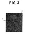
- Figure 3 shows an example of the present invention. This is an example, in which a reversed image of a digital photograph is converted into a dot pattern on a cemented carbide alloy mold by means of YVO 4 laser. The pattern is drawn in the foregoing method.
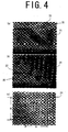
- Figure 4 is another example of the present invention, in which a letter "N" is formed also onto the cemented carbide alloy mold.
- (a) is an perspective view of the surface after formed
- (b) is an enlarged view of (a)
- (c) is also an enlarged view of a dot array observed from the top.
- Figure 5 shows another example of the present invention, which is a view of a case in which an image pattern made with a digital camera is laser processed onto the mold, and then reversely replicated onto the metallic glass.
Landscapes
- Engineering & Computer Science (AREA)
- Mechanical Engineering (AREA)
- Physics & Mathematics (AREA)
- Optics & Photonics (AREA)
- Plasma & Fusion (AREA)
- Health & Medical Sciences (AREA)
- General Health & Medical Sciences (AREA)
- Toxicology (AREA)
- Laser Beam Processing (AREA)
- Moulds For Moulding Plastics Or The Like (AREA)
- Mounting, Exchange, And Manufacturing Of Dies (AREA)
Abstract
Description
- The present invention relates to an image pattern forming method used for forming a design onto a surface of metallic glass or for adding a decorative pattern, an image, a letter to the surface of the metallic glass (e.g. a mechanical component), a device for forming the image pattern, and a metallic glass with the image pattern formed onto the surface thereof.
- In order to form a surface design of a resin-made mechanical product, a photographic image has been directly inscribed by laser marking on a product (e.g. Patent Document 1: Japanese Patent Laid-Open Application No.
2005-152968 2004-115901 2004-291288 - There have been problems with the conventional image pattern forming methods as below.
- (a) First, in the method of laser marking directly onto the product shown in
Patent Documents 1 and 2, to inscribe a fine pattern onto a large number of products with positional accuracy, a large amount of machining time and a large number of devices to execute the operation are required, and consequently, operating efficiency becomes worse. - (b) Next, with using the method described in Patent Document 3, a large number of resin products having fine patterns can be formed by the laser marking onto the mold cavity for resin molding, and then efficiently reverse transferring the patterns to the resin product. But this method could not be used for forming a metallic glass and a metal.
- (c) Further, with using the method described in Non-Patent Document 4, a pattern can be transferred to a metallic glass. But a large number of mold producing steps requires taking a long period of time, it makes the cost of the mold high accordingly. Because lithography and Ni electro forming are used for the method. Further, the mold for Ni electro forming can be used for a Pd based metallic glass, which has a low supercooled liquid temperature range and is press-formed at not higher than 400°C. But the mold cannot be used for Zr based, Ti based, Cu based, Ni based and Fe based metallic glass, which supercooled liquid temperature ranges are not lower than 400°C (which are press-formed at not lower than 400°C), and consequently, the strength of the mold is insufficient.
- In order to solve the foregoing problems, the present inventors conducted trials of a variety of methods, conditions and dedicated devices in which the number of operating steps required for pattern formation is small and the pattern forming operation itself is efficient, and which are also applicable to press-forming at not lower than 400°C, and proceeded their tests and studies. As a result, the present inventors have found that, a reversely replicated pattern can be repeatedly formed in a simple and efficient manner especially onto the surfaces of Zr based, Ti based, Cu based, Ni based and Fe based metallic glass with the surface of a heat-resistant metal-made mold which is irradiated with high energy density light to form a pattern.
- It has been further found at that time that a clear image pattern can be expressed by dividing a worked area on the mold surface into rectangular domains each having one side length of not smaller than 10 µm and not larger than 500 µm, dividing the inside of each of the rectangular domains into M by N units (3≤M,N≤10; M and N are integers) of regions to determine a resolution, and providing, or not providing, dot holes in each of the M by N units of divided regions (and further controlling the depth of the dot worked holes) to form a shaded dots assembled pattern onto the mold.
- With such the method, the image pattern becomes clearer, thereby enabling further reduction in time for generating an NC program which controls an irradiation pattern of the high energy density light and for the irradiation process. On the basis of such findings, the present inventors further conducted extensive studies, to reach completion of the present invention based upon a device with a basic configuration shown in
FIG. 1 . - In accordance with a first aspect of the present invention, a method for forming an image pattern onto a surface of the
metallic glass member 1, comprising: (a) preparing a bitmap data being mirror reversed with respect to a real image; (b) forming the image pattern as dots assembled pattern onto a surface of a mold in accordance with the bitmap data by flashing highenergy density light 15 repeatedly and scanning the surface of themold 20 while forming onedot hole 24 by one-time irradiation of the highenergy density light 15; and (c) reverse replicating the dots assembled pattern onto the metallic glass within a supercooled liquid temperature range Tg-Tx by means of themold 20 which is for dots assembled pattern formation. - A worked area of the surface of the
mold 20 may be divided into rectangular domains each having one side length of not smaller than 10 µm and not larger than 500 µm; the dots assembled pattern may have shades; the shades may be formed by forming the dot holes or not within each of the rectangular domains - The surface of the
mold 20 may be divided into rectangular domains each having one side length of not smaller than 10 µm and not larger than 500 µm; each of the rectangular domains may be divided into M by N units (3≤M,N≤10; M and N are integers) of regions for setting a resolution; the dots assembledpattern 21 may have shades; the shades may be formed by forming thedot holes 24 or not within each of the regions. - Power of the high
energy density light 15 may be controlled so as to make a depth of thedot hole 24 not smaller than 0.1 µm and not larger than 10 µm. - The
mold 20 may be made of a cemented carbide alloy. - The high
energy density light 15 may be laser light. - The metallic glass may be Zr based, Ti based, Ni based, Cu based or Fe based metallic glass
- In accordance with a second aspect of the present invention, a device for forming an image pattern onto a surface of a
metallic glass 1 with amold 20, comprising:(a) adigital processing device 10 for preparing a bitmap data being mirror reversed with respect to a real image; (b) a software for dividing a worked area of the surface of themold 20 into rectangular domains each having one side length of not smaller than 10 µm and not larger than 500 µm, dividing each of the rectangular domains into M by N units (3≤M,N≤10; M and N are integers) of regions, and making on/of signals for formingdot holes 24 or not respectively within each of the regions; - (c) a
control computer 12 for scanning while repeatedly flashing output of highenergy density light 15; - (d) an
oscillator 14 for generating highenergy density light 15 by means of a control signal, amirror 19 in a galvanometeroptical scanner 18 for scanning with the highenergy density light 15, asample stage 28 for holding themold 20; and - (e) a warm press-forming
device 30 for transferring a mirror reversed image pattern on the surface of themold 20 onto themetallic glass 1 within a supercooled liquid temperature range (Tg-Tx). - In accordance with a third aspect of the present invention, a
metallic glass 1, comprising; a surface formed an image pattern with shades by assembly of dot holes in accordance with a bitmap data. - The shades may be formed by any one of the methods of the present invention.
- The method or the device of the present invention has made it possible to form a pattern efficiently with positional accuracy onto metallic glass, especially even onto Zr based, Ti based, Cu based, Ni based and Fe based metallic glass , which have supercooled liquid temperature ranges of not lower than 400°C and are also required to be press-formed at not lower than 400°C, in large number with the simple operating steps required for pattern formation.
-
-
Figure 1 is a view showing a basic configuration of a device of the present invention; -
Figure 2 is a process chart showing a typical image pattern forming method of the present invention; -
Figure 3 is a front view of the mold, which is an example of the present invention, on which a reversed image of a digital photograph in dot pattern is drawn; -
Figure 4 is a front view of the mold, which is an example of the present invention, on which a letter "N" is drawn; and -
Figure 5 is a front view of the metallic glass on which an image pattern made with a digital camera and laser processed onto a mold are transferred. - A preferred embodiment of the present invention is described below.
Figure 1 is a basic device configuration of the present invention.Figure 2 is a process chart showing a flow of a basic process of the present invention, where the following procedure has been adopted: "inputting a digital data of an image pattern" → "making mirror reversed bitmap data" → "determining a domain size" → "converting into bitmap data with N shading gradation" → "converting into NC data for controlling power of high energy density light (laser) and position of it on a coordinate" → "applying the high energy density light (laser) with controlling the power of high energy density light (laser) and the position of it on a coordinate" → "forming a reversed image pattern onto the mold surface" → "warm press-forming a metallic glass so as to reversely replicate the image pattern of the mold thereto". Further, as described later, "determining a domain size" → "converting into bitmap data with N shading gradation" may be deleted, and the process shifts from "producing mirror reversed bitmap data" to "converting into NC data for controlling power of high energy density light (laser) and position of it on a coordinate". - In the present invention, first, an image pattern is converted into bitmap data being mirror reversed with respect to a real image. The real image is a digital photograph captured by a digital camera or an analog image (analog photograph, painting, or other analog images). "Input of data" means reading a digital data of the digital photograph and digitizing the analog image by a digital device (not shown), and converting the digitized data into a bitmap by a
digital processing device 10 such as a personal computer. Then, the image pattern is converted into the bitmap data by mirror reversing with respect to the real image. - Next, high
energy density light 15 is repeatedly flashed. Themold surface 22 is scanned while onedot holes 24 is formed with each irradiation of the highenergy density light 15, to form an image pattern as a dots assembledpattern 21 onto themold surface 22 in accordance with the bitmap data. The highenergy density light 15 may for example be YAG laser light, YVO4 laser light that is to be most easily handled, infrared laser, ultraviolet laser, or the like. Further, the highenergy density light 15 may be laser light having a conversion wavelength from its higher harmonic wave. Moreover, an electron beam may be used. - Furthermore, as for the
mold 20, a cemented carbide alloy (WC-Co alloy), which is heat resistant and has high hardness is preferably selected in a case where themold 20 is used for image transfer to a metallic glass at a temperature not lower than 400°C. Another hard metal material such as a hot work tool steel may also be selected. Further, themold 20 may be previously formed into three-dimensional shape in line with the shape of themetallic glass 1 as a member to which an image is reversely replicated. The workedsurface 22 of themold 20 preferably has a smooth flat shape so as to be in a mirror surface state, but another pattern may be previously inscribed to the workedsurface 22 by machining, etching processing (embossed pattern working), or the like. - The image pattern formed
surface 22 of themold 20 is worked by forming dots assembledpattern 21 onto themold surface 22 in accordance with the bitmap data. In the present invention, it is preferable to work on each of domains of divided rectangles (squares are adopted in the present example) each having sides length of not smaller than 10 µm and not larger than 500 µm. Each domains is divided into M by N units (33≤M,N≤10; M and N are integers) of regions, and then subjected to processing of dot holes (including no dot hole). The reason that the worked area on themold 20 is divided into the rectangular domains is to regulate a working speed. If the sides are smaller than 10 µm, the division is too fine to be realistic in terms of time for data processing and the working. On the other hand, if the sides are larger than 500 µm, the time for the processing and working are short, but the image pattern loses its clearness, and consequently, its appearance becomes significantly poor with respect to the real image. (The length of sides are uniformed each other in length and width in this case, but the length of the sides can be made different each other in the length and width.) - The reason that each rectangular domain is divided into M by N units of regions, and each of M and N is not smaller than 3 and not larger than 10 is as follows. If each of M and N is smaller than 3, the amount of information for expressing the shape outline is reduced, causing significant deterioration in image quality at the time of conversion of a fine picture pattern such as a photograph into the bitmap data. On the other hand, if each of M and N is larger than 10, the resolution increases. But classification operation processing on data to have shading gradation takes too long time. (The length and width of region may be the same each other [or may be different (= rectangular domain)], and the number of division of the region may be the same N [or may be different as described above], to give a square domain. In addition, the dot holes may be made in accordance with the bitmap data without the division of the rectangular domains.
- The shades of the image pattern are expressed by density of dots formed onto the surface. Furthermore, the depth of the dot holes 24 may be changed in the range of not smaller than 0.1 µm and not larger than 10 µm. The reason is that as follows. If the depth of the dot holes 24 is smaller than 0.1 µm, unclear shade makes the image pattern blurred. On the other hand, if the depth of the dot holes 24 is larger than 10 µm, the shading is clear, but the dot holes 24 make the metallic glass surface rough that appears and is sensed by touching with a hand, which is unfavorable.
- This dot hole processing is executed with the high
energy density light 15 such as laser light applied from theoscillator 14 by means of a control signal from thecontrol computer 12. And the bitmap data with N shading gradation is converted into NC data for controlling the power of the high energy density light (laser) and the position of it on a coordinate. The highenergy density light 15, which is reflected on themirror 19 in the galvanometeroptical scanner 18, scans the image pattern formedsurface 22 of themold 20. And the highenergy density light 15, which is controlled by software loaded on thecontrol computer 12 makes the dot holes in line with an on/off signal based upon the NC data. The depth of the dot holes is controlled based upon the power of the highenergy density light 15 as described above. When the depth of the dot holes are controlled, the power of the highenergy density light 15 is controlled such that the depth of the dot holes 24 are not smaller than 0.1 µm and not larger than 10 µm as described above. The depth of the dot holes may be uniformed each other. - The
mirror 19 in the galvanometeroptical scanner 18 makes the highenergy density light 15 scans the image pattern formedsurface 22 with changing reflection angles of the highenergy density light 15. - The software loaded on the
control computer 12 includes the image pattern information such as division information for dividing the image pattern formed surface into the rectangular domains, and conversion information for processing bitmap data, which is to be allocated to each of the domains, into M by N units (3≤M,N≤10; M and N are integers) of shading gradation, and thereafter converting the gradation into on/off signals representing presence or absence of the dot holes 24 on the image pattern formation surface (as well as "power" information of the highenergy density light 15 in the case of controlling its power). - The
sample stage 28, which serves to hold the mold, is installed to receive the highenergy density light 15 such as laser light applied from theoscillator 14. - As shown in
Figure 1 , a warm press-formingdevice 30 comprises achamber 31 having atemperature control heater 32, and a pair of die bases 35 (lower) and 36 (upper). And inside of thechamber 31 is filled and aerated with high vacuum or inert gases (helium, nitrogen, argon gas, etc.) so that the warm press-forming can be performed within a non-oxidizing atmosphere. Themetallic glass 1 which is set within thechamber 31 can be accessed through an open/close section (not shown). (It is to be noted that, the warm press-forming may be performed under the oxidizing atmosphere such as air. In this case, the warm press-forming should be rapidly performed so as to be completed before crystallization, whereby an oxide film of the surface of themetallic glass 1 can serve as a protection film so as to prevent oxidization inside. And so long as such a condition is satisfied, the warm press-forming can also be performed in the air.) Thedie base 35 is for being loaded with the mold. Thedie base 36 is for pressing themetallic glass 1 onto themold 20. In the case of the present example, thedie base 36 presses themetallic glass 1 onto themold 20. Themetallic glass 1 is held at the temperature within the supercooled liquid temperature range Tg-Tx by thetemperature control heater 32 inside thechamber 31 of the warm press-formingdevice 30. - With the warm press-forming
device 30, it is possible to form the superfine reverse replica onto themetallic glass 1 with themold 20 within the supercooled liquid temperature range [Tg (metallic glass transition start temperature) to Tx (metallic glass transition end temperature); within this range, a viscous flowing property like a glass is obtained and a pattern as superfine as a nano size can be formed (or replicated)]. - As for the metallic glass, Zr based, Ti based, Ni based, Cu based or Fe based metallic glass is preferred. Because those types of metallic glass which have relatively broad supercooled liquid temperature ranges contain no high-priced metal element as the main constituent element, the low cost of metallic glass makes this method an economical process.
-
Figure 3 shows an example of the present invention. This is an example, in which a reversed image of a digital photograph is converted into a dot pattern on a cemented carbide alloy mold by means of YVO4 laser. The pattern is drawn in the foregoing method. Further,Figure 4 is another example of the present invention, in which a letter "N" is formed also onto the cemented carbide alloy mold. (a) is an perspective view of the surface after formed, (b) is an enlarged view of (a), and (c) is also an enlarged view of a dot array observed from the top.Figure 5 shows another example of the present invention, which is a view of a case in which an image pattern made with a digital camera is laser processed onto the mold, and then reversely replicated onto the metallic glass. - According to the present invention, it becomes possible to form an image pattern especially on the surfaces of Zr based, Ti based, Ni based, Cu based and Fe based metallic glass that are required to be press-formed at not lower than 400°C, which has not hitherto been realizable, so as to significantly enhance industrial availabilities of these types of metallic glass.
Claims (10)
- A method for forming an image pattern onto a surface of a metallic glass, comprising:(a) preparing bitmap data, which is mirror reversed with respect to a real image;(b) forming the image pattern as an assembled pattern of dots onto a surface of a mold in accordance with the bitmap data by flashing high energy density light repeatedly and scanning the surface of the mold while forming one dot hole at each irradiation of the high energy density light; and(c) reversely replicating the assembled pattern of dots onto the metallic glass within a supercooled liquid temperature range by means of the mold.
- The method according to claim 1, wherein a processed area of the surface of the mold is divided into rectangular domains each having one side length of not smaller than 10 µm and not larger than 500 µm;
the assembled pattern of dots has shades;
the shades are formed by forming the dot holes or not within each of the rectangular domains. - The method according to claim 1, wherein the surface of the mold is divided into rectangular domains each having one side length of not smaller than 10 µm and not larger than 500 µm;
each of the rectangular domains is divided into M by N units (3≤M,N≤10; M and N are integers) of regions for setting a resolution;
the assembled pattern of dots has shades;
the shades are formed by forming the dot holes or not within each of the regions. - The method according to any one of claims 1 to 3, wherein power of the high energy density light is controlled so as to make a depth of the dot hole not smaller than 0.1 µm and not larger than 10 µm.
- The method according to any one of claims 1 to 4, wherein the mold is made of a cemented carbide alloy.
- The method according to any one of claims 1 to 5, wherein the high energy density light is laser light.
- The method according to any one of claims 1 to 6, wherein the metallic glass is Zr based, Ti based, Ni based, Cu based or Fe based metallic glass.
- A device for forming an image pattern onto a surface of a metallic glass with a mold, comprising:(a) a digital processing device for preparing bitmap data, which is mirror reversed with respect to a real image;(b) a software for dividing a processed area of the surface of the mold into rectangular domains each having one side length of not smaller than 10 µm and not larger than 500 µm, dividing each of the rectangular domains into M by N units (3≤M,N≤10; M and N are integers) of regions, and making on/of signals for forming dot holes or not respectively within each of the regions;(c) a control computer for scanning while repeatedly flashing output of high energy density light;(d) an oscillator for generating high energy density light by means of a control signal, a mirror for scanning with the high energy density light, a sample stage for holding the mold; and(e) a warm press-forming device for replicating a mirror reversed image pattern on the surface of the mold onto the metallic glass within a supercooled liquid temperature range.
- A metallic glass, comprising:a surface on which an image pattern with shades is formed by an assembly of dot holes in accordance with bitmap data.
- The metallic glass according to claim 9, wherein the shades is formed by any one of the methods according to claims 1 to 7.
Applications Claiming Priority (2)
| Application Number | Priority Date | Filing Date | Title |
|---|---|---|---|
| JP2005359305 | 2005-12-13 | ||
| PCT/JP2006/320201 WO2007069385A1 (en) | 2005-12-13 | 2006-10-10 | Method for forming image pattern on surface of metallic glass member, apparatus for forming image pattern, and metallic glass member having image pattern on its surface |
Publications (3)
| Publication Number | Publication Date |
|---|---|
| EP1964622A1 true EP1964622A1 (en) | 2008-09-03 |
| EP1964622A4 EP1964622A4 (en) | 2009-11-11 |
| EP1964622B1 EP1964622B1 (en) | 2013-01-23 |
Family
ID=38162700
Family Applications (1)
| Application Number | Title | Priority Date | Filing Date |
|---|---|---|---|
| EP06811514A Not-in-force EP1964622B1 (en) | 2005-12-13 | 2006-10-10 | Method of forming an image pattern on surface of a metallic glass member |
Country Status (6)
| Country | Link |
|---|---|
| US (1) | US20090044924A1 (en) |
| EP (1) | EP1964622B1 (en) |
| JP (1) | JP5407013B2 (en) |
| KR (1) | KR101360805B1 (en) |
| CN (1) | CN101300091B (en) |
| WO (1) | WO2007069385A1 (en) |
Cited By (1)
| Publication number | Priority date | Publication date | Assignee | Title |
|---|---|---|---|---|
| WO2012072740A1 (en) * | 2010-12-03 | 2012-06-07 | Basf Se | Method for producing multi-layer composite bodies |
Families Citing this family (11)
| Publication number | Priority date | Publication date | Assignee | Title |
|---|---|---|---|---|
| RS52165B (en) * | 2009-08-26 | 2012-08-31 | Indaffil Holding Ag | PROCEDURE FOR THE DESIGN OF A SURFACE STRUCTURE OF A METAL PRESSURE PLATE, ENDLESS BAND OR ENGRAVING ROLLER |
| CN102686074A (en) * | 2011-03-08 | 2012-09-19 | 鸿富锦精密工业(深圳)有限公司 | Electronic device shell and manufacture method thereof |
| CN103170727B (en) * | 2011-12-26 | 2015-12-09 | 武汉金运激光股份有限公司 | Laser galvanometer bitmap processing mode |
| CN102581109B (en) * | 2012-03-26 | 2014-05-28 | 江苏大学 | Method for manufacturing non-smooth surface of organism and device |
| CN102615820A (en) * | 2012-04-12 | 2012-08-01 | 中国科学院物理研究所 | Metallic glass-based plastic thermal embossing micro-molding mold and preparation method thereof |
| CN103273157B (en) * | 2013-05-31 | 2015-08-19 | 哈尔滨工业大学 | A kind of method accelerating Zr bast block metal glass and Sn base solder metallurgical binding |
| CN103286406B (en) * | 2013-05-31 | 2015-10-07 | 哈尔滨工业大学 | The low temperature method of attachment of a kind of Zr bast block metal glass and Sn base solder |
| KR101483966B1 (en) * | 2013-07-03 | 2015-01-22 | 이은상 | laser marking method of metal panel |
| CN104754888A (en) * | 2013-12-25 | 2015-07-01 | 正达国际光电股份有限公司 | Glass case, molding die and molding method for manufacturing the glass case |
| CN107790536A (en) * | 2017-10-17 | 2018-03-13 | 深圳大学 | Glassy metal embossing forming device |
| CN112108774B (en) * | 2020-09-04 | 2022-07-01 | 深圳泰软软件科技有限公司 | Three-dimensional laser bitmap marking method and device and computer readable storage medium |
Family Cites Families (25)
| Publication number | Priority date | Publication date | Assignee | Title |
|---|---|---|---|---|
| JPH0230306A (en) * | 1988-07-15 | 1990-01-31 | Sumitomo Metal Ind Ltd | Metal sheet having good surface quality and manufacturing method and rolling roll used in manufacture of above mentioned sheet |
| CN1034060C (en) * | 1993-08-25 | 1997-02-19 | 史庭兆 | Method of forming gold photo |
| DE4441337A1 (en) * | 1994-11-08 | 1996-05-09 | Thomas Elm | Application of pattern onto steel plate by laser process |
| US5950704A (en) * | 1996-07-18 | 1999-09-14 | Amorphous Technologies International | Replication of surface features from a master model to an amorphous metallic article |
| JP3315916B2 (en) * | 1998-01-08 | 2002-08-19 | 日立建機株式会社 | Laser marking device |
| JP2951646B1 (en) * | 1998-06-26 | 1999-09-20 | ニチハ株式会社 | Surface shape data creation system and recording medium |
| JP2001314984A (en) * | 2000-05-01 | 2001-11-13 | Rofin Marubeni Laser Kk | Laser stamping method and apparatus for metal mold |
| US6620264B2 (en) * | 2000-06-09 | 2003-09-16 | California Institute Of Technology | Casting of amorphous metallic parts by hot mold quenching |
| JP2002244370A (en) * | 2000-11-16 | 2002-08-30 | Canon Inc | Image forming apparatus and method, process cartridge |
| JP2002351241A (en) * | 2001-05-29 | 2002-12-06 | Canon Inc | Image forming device |
| JP2003117647A (en) * | 2001-10-09 | 2003-04-23 | Ykk Corp | Hollow casting with slit, and manufacturing method and manufacturing device thereof |
| JP3495359B2 (en) * | 2001-12-21 | 2004-02-09 | コニカミノルタホールディングス株式会社 | Marking method for photosensitive material |
| JP4204293B2 (en) | 2002-09-30 | 2009-01-07 | アイシン軽金属株式会社 | Image forming method on aluminum alloy surface |
| JP4507591B2 (en) * | 2003-01-09 | 2010-07-21 | 東洋製罐株式会社 | Pattern transfer can and manufacturing method thereof |
| JP2004291288A (en) | 2003-03-26 | 2004-10-21 | Sunarrow Ltd | Mold cavity for resin molding and method of manufacturing the same |
| JP2005093391A (en) * | 2003-09-19 | 2005-04-07 | Daido Steel Co Ltd | Metal separator for fuel cell, manufacturing method of metal separator for fuel cell, and fuel cell |
| DE10345080A1 (en) * | 2003-09-26 | 2005-05-12 | Peguform Gmbh | Method and device for layer-removing 3-dimensional material processing |
| JP2005121730A (en) * | 2003-10-14 | 2005-05-12 | Seiko Epson Corp | Reflective diffraction grating and method of manufacturing the same |
| JP2005138169A (en) * | 2003-11-10 | 2005-06-02 | Gijutsu Transfer Service:Kk | Laser marking device, laser marking method, and object to be marked |
| JP2005152968A (en) | 2003-11-27 | 2005-06-16 | Techno Polymer Co Ltd | Image marking device for cellular phone |
| JP2005152966A (en) * | 2003-11-27 | 2005-06-16 | Fuji Photo Film Co Ltd | Laser processing method and material transfer method |
| JP2005186080A (en) * | 2003-12-24 | 2005-07-14 | Gijutsu Transfer Service:Kk | Laser marking device and laser marking method |
| EP2479309B1 (en) * | 2004-03-25 | 2016-05-11 | Tohoku Techno Arch Co., Ltd. | Metallic glass laminates, production methods and applications thereof |
| JP4693772B2 (en) * | 2004-05-28 | 2011-06-01 | 日本碍子株式会社 | Metal glass forming method |
| US20050277286A1 (en) * | 2004-06-14 | 2005-12-15 | Daewoong Suh | Metallic glass microtool |
-
2006
- 2006-10-10 WO PCT/JP2006/320201 patent/WO2007069385A1/en not_active Ceased
- 2006-10-10 JP JP2007550090A patent/JP5407013B2/en not_active Expired - Fee Related
- 2006-10-10 US US12/097,189 patent/US20090044924A1/en not_active Abandoned
- 2006-10-10 EP EP06811514A patent/EP1964622B1/en not_active Not-in-force
- 2006-10-10 CN CN2006800413370A patent/CN101300091B/en not_active Expired - Fee Related
- 2006-10-10 KR KR1020087013458A patent/KR101360805B1/en not_active Expired - Fee Related
Cited By (1)
| Publication number | Priority date | Publication date | Assignee | Title |
|---|---|---|---|---|
| WO2012072740A1 (en) * | 2010-12-03 | 2012-06-07 | Basf Se | Method for producing multi-layer composite bodies |
Also Published As
| Publication number | Publication date |
|---|---|
| KR101360805B1 (en) | 2014-02-11 |
| CN101300091B (en) | 2011-06-08 |
| US20090044924A1 (en) | 2009-02-19 |
| EP1964622B1 (en) | 2013-01-23 |
| CN101300091A (en) | 2008-11-05 |
| JP5407013B2 (en) | 2014-02-05 |
| JPWO2007069385A1 (en) | 2009-05-21 |
| WO2007069385A1 (en) | 2007-06-21 |
| EP1964622A4 (en) | 2009-11-11 |
| KR20080076925A (en) | 2008-08-20 |
Similar Documents
| Publication | Publication Date | Title |
|---|---|---|
| EP1964622B1 (en) | Method of forming an image pattern on surface of a metallic glass member | |
| US5329381A (en) | Automatic engraving method and apparatus | |
| EP3652676B1 (en) | 3d printed identification labels | |
| US5116174A (en) | Method and apparatus for manufacturing jewelry, and an article of jewelry made thereby | |
| CN108817674A (en) | A kind of dual-beam five-shaft numerical control laser polishing method | |
| BG64251B1 (en) | Process for producing dies, engraved object, made by the process, and application of the engaved object | |
| WO2005104005A1 (en) | Method for forming 2-dimensional code by laser marking and laser marking device | |
| JP2008265344A (en) | Color marking method using laser | |
| US7126619B2 (en) | System and method for direct laser engraving of images onto a printing substrate | |
| Hubeatir et al. | A review: Effect of different laser types on material engraving process | |
| Friedrich et al. | Precision structuring and functionalization of ceramics with ultra-short laser pulses | |
| US5804342A (en) | Method of bar-code printing on ceramic members | |
| JPH01114423A (en) | Laser etching method of foaming base material | |
| US20020092322A1 (en) | Refrigerator art jewelry | |
| KR20010054712A (en) | Engraving a photo, a picture or letters on a stone with laser technology | |
| CN114571087A (en) | Laser engraving method capable of editing curved surface 3D texture | |
| JP2004358662A (en) | Method of making uneven pattern and stamping die and stamping die | |
| JPH11119409A (en) | Method and apparatus for creating a printing plate for a three-dimensional object | |
| KR20240093631A (en) | How to engrave a code pattern on the tool surface of a solid piece | |
| JP2000006597A (en) | Processed paper | |
| US6520049B2 (en) | Method of digitizing emboss dies and the like | |
| JP3655879B2 (en) | Laser beam engraving method | |
| JP3094612U (en) | Decorative pattern | |
| Duc et al. | Ceramic engraving using pulse fiber laser: numerical simulation and experiment | |
| JP2004082493A (en) | A method of drawing various color patterns on a special oxide-coated metal plate with a laser |
Legal Events
| Date | Code | Title | Description |
|---|---|---|---|
| PUAI | Public reference made under article 153(3) epc to a published international application that has entered the european phase |
Free format text: ORIGINAL CODE: 0009012 |
|
| 17P | Request for examination filed |
Effective date: 20080709 |
|
| AK | Designated contracting states |
Kind code of ref document: A1 Designated state(s): DE FI FR GB |
|
| RAP1 | Party data changed (applicant data changed or rights of an application transferred) |
Owner name: NGK INSULATORS, LTD. |
|
| DAX | Request for extension of the european patent (deleted) | ||
| RBV | Designated contracting states (corrected) |
Designated state(s): DE FI FR GB |
|
| RIC1 | Information provided on ipc code assigned before grant |
Ipc: B23K 26/00 20060101ALI20090827BHEP Ipc: B21D 22/02 20060101AFI20070813BHEP Ipc: B22D 23/00 20060101ALI20090827BHEP Ipc: B21D 37/00 20060101ALI20090827BHEP Ipc: B41M 5/26 20060101ALI20090827BHEP Ipc: B29C 33/38 20060101ALI20090827BHEP Ipc: B44C 1/22 20060101ALI20090827BHEP |
|
| RA4 | Supplementary search report drawn up and despatched (corrected) |
Effective date: 20090914 |
|
| A4 | Supplementary search report drawn up and despatched |
Effective date: 20090914 |
|
| 17Q | First examination report despatched |
Effective date: 20100520 |
|
| GRAP | Despatch of communication of intention to grant a patent |
Free format text: ORIGINAL CODE: EPIDOSNIGR1 |
|
| GRAS | Grant fee paid |
Free format text: ORIGINAL CODE: EPIDOSNIGR3 |
|
| GRAA | (expected) grant |
Free format text: ORIGINAL CODE: 0009210 |
|
| AK | Designated contracting states |
Kind code of ref document: B1 Designated state(s): DE FI FR GB |
|
| REG | Reference to a national code |
Ref country code: GB Ref legal event code: FG4D |
|
| REG | Reference to a national code |
Ref country code: DE Ref legal event code: R096 Ref document number: 602006034390 Country of ref document: DE Effective date: 20130321 |
|
| PLBE | No opposition filed within time limit |
Free format text: ORIGINAL CODE: 0009261 |
|
| STAA | Information on the status of an ep patent application or granted ep patent |
Free format text: STATUS: NO OPPOSITION FILED WITHIN TIME LIMIT |
|
| 26N | No opposition filed |
Effective date: 20131024 |
|
| REG | Reference to a national code |
Ref country code: DE Ref legal event code: R097 Ref document number: 602006034390 Country of ref document: DE Effective date: 20131024 |
|
| REG | Reference to a national code |
Ref country code: FR Ref legal event code: PLFP Year of fee payment: 11 |
|
| PGFP | Annual fee paid to national office [announced via postgrant information from national office to epo] |
Ref country code: FR Payment date: 20160919 Year of fee payment: 11 |
|
| PGFP | Annual fee paid to national office [announced via postgrant information from national office to epo] |
Ref country code: GB Payment date: 20161005 Year of fee payment: 11 Ref country code: DE Payment date: 20161004 Year of fee payment: 11 Ref country code: FI Payment date: 20161010 Year of fee payment: 11 |
|
| REG | Reference to a national code |
Ref country code: DE Ref legal event code: R119 Ref document number: 602006034390 Country of ref document: DE |
|
| GBPC | Gb: european patent ceased through non-payment of renewal fee |
Effective date: 20171010 |
|
| REG | Reference to a national code |
Ref country code: FR Ref legal event code: ST Effective date: 20180629 |
|
| PG25 | Lapsed in a contracting state [announced via postgrant information from national office to epo] |
Ref country code: GB Free format text: LAPSE BECAUSE OF NON-PAYMENT OF DUE FEES Effective date: 20171010 Ref country code: FI Free format text: LAPSE BECAUSE OF NON-PAYMENT OF DUE FEES Effective date: 20171010 Ref country code: DE Free format text: LAPSE BECAUSE OF NON-PAYMENT OF DUE FEES Effective date: 20180501 |
|
| PG25 | Lapsed in a contracting state [announced via postgrant information from national office to epo] |
Ref country code: FR Free format text: LAPSE BECAUSE OF NON-PAYMENT OF DUE FEES Effective date: 20171031 |