EP1962668B1 - Sandwich sensor for the determination of an analyte concentration - Google Patents
Sandwich sensor for the determination of an analyte concentration Download PDFInfo
- Publication number
- EP1962668B1 EP1962668B1 EP06819917A EP06819917A EP1962668B1 EP 1962668 B1 EP1962668 B1 EP 1962668B1 EP 06819917 A EP06819917 A EP 06819917A EP 06819917 A EP06819917 A EP 06819917A EP 1962668 B1 EP1962668 B1 EP 1962668B1
- Authority
- EP
- European Patent Office
- Prior art keywords
- electrode
- layer
- implantable sensor
- carrier substrate
- electrode contact
- Prior art date
- Legal status (The legal status is an assumption and is not a legal conclusion. Google has not performed a legal analysis and makes no representation as to the accuracy of the status listed.)
- Active
Links
- 239000012491 analyte Substances 0.000 title claims abstract description 32
- 239000000758 substrate Substances 0.000 claims abstract description 121
- 239000012528 membrane Substances 0.000 claims abstract description 44
- 210000001124 body fluid Anatomy 0.000 claims abstract description 25
- 238000000034 method Methods 0.000 claims description 124
- 239000012212 insulator Substances 0.000 claims description 37
- 238000004519 manufacturing process Methods 0.000 claims description 28
- 238000003780 insertion Methods 0.000 claims description 23
- 230000037431 insertion Effects 0.000 claims description 23
- 210000001519 tissue Anatomy 0.000 claims description 23
- 238000005520 cutting process Methods 0.000 claims description 20
- 238000000576 coating method Methods 0.000 claims description 15
- 229910052751 metal Inorganic materials 0.000 claims description 12
- 239000002184 metal Substances 0.000 claims description 12
- 239000000126 substance Substances 0.000 claims description 8
- 239000002313 adhesive film Substances 0.000 claims description 7
- 229920002635 polyurethane Polymers 0.000 claims description 6
- 239000004814 polyurethane Substances 0.000 claims description 6
- 238000010030 laminating Methods 0.000 claims description 4
- 229920000642 polymer Polymers 0.000 claims description 4
- 210000000577 adipose tissue Anatomy 0.000 claims description 3
- 238000005229 chemical vapour deposition Methods 0.000 claims description 3
- 229920000728 polyester Polymers 0.000 claims description 3
- 239000011810 insulating material Substances 0.000 claims description 2
- 239000010839 body fluid Substances 0.000 abstract description 21
- 238000010276 construction Methods 0.000 abstract description 10
- 239000010410 layer Substances 0.000 description 293
- 239000000463 material Substances 0.000 description 25
- WQZGKKKJIJFFOK-GASJEMHNSA-N Glucose Natural products OC[C@H]1OC(O)[C@H](O)[C@@H](O)[C@@H]1O WQZGKKKJIJFFOK-GASJEMHNSA-N 0.000 description 22
- 239000008103 glucose Substances 0.000 description 22
- NUJOXMJBOLGQSY-UHFFFAOYSA-N manganese dioxide Chemical compound O=[Mn]=O NUJOXMJBOLGQSY-UHFFFAOYSA-N 0.000 description 22
- 238000005259 measurement Methods 0.000 description 21
- 239000010408 film Substances 0.000 description 19
- 230000008569 process Effects 0.000 description 19
- 108010015776 Glucose oxidase Proteins 0.000 description 17
- 239000004366 Glucose oxidase Substances 0.000 description 15
- 229940116332 glucose oxidase Drugs 0.000 description 15
- 235000019420 glucose oxidase Nutrition 0.000 description 15
- 239000008280 blood Substances 0.000 description 14
- 210000004369 blood Anatomy 0.000 description 14
- 229910021607 Silver chloride Inorganic materials 0.000 description 13
- 238000009792 diffusion process Methods 0.000 description 13
- HKZLPVFGJNLROG-UHFFFAOYSA-M silver monochloride Chemical compound [Cl-].[Ag+] HKZLPVFGJNLROG-UHFFFAOYSA-M 0.000 description 13
- 239000011888 foil Substances 0.000 description 8
- 108090000790 Enzymes Proteins 0.000 description 7
- 102000004190 Enzymes Human genes 0.000 description 7
- 239000011248 coating agent Substances 0.000 description 7
- 239000003792 electrolyte Substances 0.000 description 7
- 229940088598 enzyme Drugs 0.000 description 7
- 230000015572 biosynthetic process Effects 0.000 description 6
- 238000005516 engineering process Methods 0.000 description 6
- NOESYZHRGYRDHS-UHFFFAOYSA-N insulin Chemical compound N1C(=O)C(NC(=O)C(CCC(N)=O)NC(=O)C(CCC(O)=O)NC(=O)C(C(C)C)NC(=O)C(NC(=O)CN)C(C)CC)CSSCC(C(NC(CO)C(=O)NC(CC(C)C)C(=O)NC(CC=2C=CC(O)=CC=2)C(=O)NC(CCC(N)=O)C(=O)NC(CC(C)C)C(=O)NC(CCC(O)=O)C(=O)NC(CC(N)=O)C(=O)NC(CC=2C=CC(O)=CC=2)C(=O)NC(CSSCC(NC(=O)C(C(C)C)NC(=O)C(CC(C)C)NC(=O)C(CC=2C=CC(O)=CC=2)NC(=O)C(CC(C)C)NC(=O)C(C)NC(=O)C(CCC(O)=O)NC(=O)C(C(C)C)NC(=O)C(CC(C)C)NC(=O)C(CC=2NC=NC=2)NC(=O)C(CO)NC(=O)CNC2=O)C(=O)NCC(=O)NC(CCC(O)=O)C(=O)NC(CCCNC(N)=N)C(=O)NCC(=O)NC(CC=3C=CC=CC=3)C(=O)NC(CC=3C=CC=CC=3)C(=O)NC(CC=3C=CC(O)=CC=3)C(=O)NC(C(C)O)C(=O)N3C(CCC3)C(=O)NC(CCCCN)C(=O)NC(C)C(O)=O)C(=O)NC(CC(N)=O)C(O)=O)=O)NC(=O)C(C(C)CC)NC(=O)C(CO)NC(=O)C(C(C)O)NC(=O)C1CSSCC2NC(=O)C(CC(C)C)NC(=O)C(NC(=O)C(CCC(N)=O)NC(=O)C(CC(N)=O)NC(=O)C(NC(=O)C(N)CC=1C=CC=CC=1)C(C)C)CC1=CN=CN1 NOESYZHRGYRDHS-UHFFFAOYSA-N 0.000 description 6
- BASFCYQUMIYNBI-UHFFFAOYSA-N platinum Chemical compound [Pt] BASFCYQUMIYNBI-UHFFFAOYSA-N 0.000 description 6
- 239000003814 drug Substances 0.000 description 5
- 239000007772 electrode material Substances 0.000 description 5
- 230000006870 function Effects 0.000 description 5
- 239000007789 gas Substances 0.000 description 5
- 238000003475 lamination Methods 0.000 description 5
- 238000007639 printing Methods 0.000 description 5
- 210000003491 skin Anatomy 0.000 description 5
- 230000008901 benefit Effects 0.000 description 4
- WQZGKKKJIJFFOK-VFUOTHLCSA-N beta-D-glucose Chemical compound OC[C@H]1O[C@@H](O)[C@H](O)[C@@H](O)[C@@H]1O WQZGKKKJIJFFOK-VFUOTHLCSA-N 0.000 description 4
- 230000008859 change Effects 0.000 description 4
- 238000013461 design Methods 0.000 description 4
- 238000001514 detection method Methods 0.000 description 4
- 238000007598 dipping method Methods 0.000 description 4
- 229940079593 drug Drugs 0.000 description 4
- 238000001035 drying Methods 0.000 description 4
- 230000002401 inhibitory effect Effects 0.000 description 4
- 239000007788 liquid Substances 0.000 description 4
- 238000005240 physical vapour deposition Methods 0.000 description 4
- 230000002829 reductive effect Effects 0.000 description 4
- 229910052709 silver Inorganic materials 0.000 description 4
- 239000004332 silver Substances 0.000 description 4
- 238000012360 testing method Methods 0.000 description 4
- 102000004877 Insulin Human genes 0.000 description 3
- 108090001061 Insulin Proteins 0.000 description 3
- JVTAAEKCZFNVCJ-UHFFFAOYSA-M Lactate Chemical compound CC(O)C([O-])=O JVTAAEKCZFNVCJ-UHFFFAOYSA-M 0.000 description 3
- 238000010292 electrical insulation Methods 0.000 description 3
- PCHJSUWPFVWCPO-UHFFFAOYSA-N gold Chemical compound [Au] PCHJSUWPFVWCPO-UHFFFAOYSA-N 0.000 description 3
- 229910052737 gold Inorganic materials 0.000 description 3
- 239000010931 gold Substances 0.000 description 3
- 229940125396 insulin Drugs 0.000 description 3
- 238000001459 lithography Methods 0.000 description 3
- 239000000203 mixture Substances 0.000 description 3
- 230000035699 permeability Effects 0.000 description 3
- 229910052697 platinum Inorganic materials 0.000 description 3
- 150000003626 triacylglycerols Chemical class 0.000 description 3
- OKTJSMMVPCPJKN-UHFFFAOYSA-N Carbon Chemical compound [C] OKTJSMMVPCPJKN-UHFFFAOYSA-N 0.000 description 2
- PHOQVHQSTUBQQK-SQOUGZDYSA-N D-glucono-1,5-lactone Chemical compound OC[C@H]1OC(=O)[C@H](O)[C@@H](O)[C@@H]1O PHOQVHQSTUBQQK-SQOUGZDYSA-N 0.000 description 2
- BQCADISMDOOEFD-UHFFFAOYSA-N Silver Chemical compound [Ag] BQCADISMDOOEFD-UHFFFAOYSA-N 0.000 description 2
- 229910052782 aluminium Inorganic materials 0.000 description 2
- XAGFODPZIPBFFR-UHFFFAOYSA-N aluminium Chemical compound [Al] XAGFODPZIPBFFR-UHFFFAOYSA-N 0.000 description 2
- 238000006243 chemical reaction Methods 0.000 description 2
- 238000007796 conventional method Methods 0.000 description 2
- 238000011161 development Methods 0.000 description 2
- 230000018109 developmental process Effects 0.000 description 2
- 238000002848 electrochemical method Methods 0.000 description 2
- 238000003487 electrochemical reaction Methods 0.000 description 2
- 235000012209 glucono delta-lactone Nutrition 0.000 description 2
- 229960003681 gluconolactone Drugs 0.000 description 2
- 238000007654 immersion Methods 0.000 description 2
- 238000000608 laser ablation Methods 0.000 description 2
- 238000000691 measurement method Methods 0.000 description 2
- 150000002739 metals Chemical class 0.000 description 2
- 239000012811 non-conductive material Substances 0.000 description 2
- 239000004033 plastic Substances 0.000 description 2
- 229920003023 plastic Polymers 0.000 description 2
- 238000007650 screen-printing Methods 0.000 description 2
- 238000004544 sputter deposition Methods 0.000 description 2
- 230000002123 temporal effect Effects 0.000 description 2
- 239000010409 thin film Substances 0.000 description 2
- 238000007740 vapor deposition Methods 0.000 description 2
- 238000007704 wet chemistry method Methods 0.000 description 2
- 241001631457 Cannula Species 0.000 description 1
- 101710112752 Cytotoxin Proteins 0.000 description 1
- UFHFLCQGNIYNRP-UHFFFAOYSA-N Hydrogen Chemical compound [H][H] UFHFLCQGNIYNRP-UHFFFAOYSA-N 0.000 description 1
- 239000000853 adhesive Substances 0.000 description 1
- 239000002390 adhesive tape Substances 0.000 description 1
- 239000002671 adjuvant Substances 0.000 description 1
- 230000002411 adverse Effects 0.000 description 1
- 238000013459 approach Methods 0.000 description 1
- QVGXLLKOCUKJST-UHFFFAOYSA-N atomic oxygen Chemical compound [O] QVGXLLKOCUKJST-UHFFFAOYSA-N 0.000 description 1
- 230000004888 barrier function Effects 0.000 description 1
- 239000000560 biocompatible material Substances 0.000 description 1
- 230000005540 biological transmission Effects 0.000 description 1
- 229910052799 carbon Inorganic materials 0.000 description 1
- 239000000919 ceramic Substances 0.000 description 1
- 239000002800 charge carrier Substances 0.000 description 1
- 238000001311 chemical methods and process Methods 0.000 description 1
- 239000003153 chemical reaction reagent Substances 0.000 description 1
- RCTYPNKXASFOBE-UHFFFAOYSA-M chloromercury Chemical compound [Hg]Cl RCTYPNKXASFOBE-UHFFFAOYSA-M 0.000 description 1
- 229920001940 conductive polymer Polymers 0.000 description 1
- 239000004020 conductor Substances 0.000 description 1
- 231100000599 cytotoxic agent Toxicity 0.000 description 1
- 239000002619 cytotoxin Substances 0.000 description 1
- 230000018044 dehydration Effects 0.000 description 1
- 238000006297 dehydration reaction Methods 0.000 description 1
- 210000004207 dermis Anatomy 0.000 description 1
- 206010012601 diabetes mellitus Diseases 0.000 description 1
- 238000002405 diagnostic procedure Methods 0.000 description 1
- 230000000694 effects Effects 0.000 description 1
- 238000005868 electrolysis reaction Methods 0.000 description 1
- 239000002001 electrolyte material Substances 0.000 description 1
- 239000008393 encapsulating agent Substances 0.000 description 1
- 238000005530 etching Methods 0.000 description 1
- 239000000284 extract Substances 0.000 description 1
- -1 for example Substances 0.000 description 1
- 229910002804 graphite Inorganic materials 0.000 description 1
- 239000010439 graphite Substances 0.000 description 1
- 230000036541 health Effects 0.000 description 1
- 229940088597 hormone Drugs 0.000 description 1
- 239000005556 hormone Substances 0.000 description 1
- 239000001257 hydrogen Substances 0.000 description 1
- 229910052739 hydrogen Inorganic materials 0.000 description 1
- 230000001771 impaired effect Effects 0.000 description 1
- 238000002513 implantation Methods 0.000 description 1
- 238000001727 in vivo Methods 0.000 description 1
- 238000009413 insulation Methods 0.000 description 1
- UETZVSHORCDDTH-UHFFFAOYSA-N iron(2+);hexacyanide Chemical compound [Fe+2].N#[C-].N#[C-].N#[C-].N#[C-].N#[C-].N#[C-] UETZVSHORCDDTH-UHFFFAOYSA-N 0.000 description 1
- 238000005304 joining Methods 0.000 description 1
- 230000007246 mechanism Effects 0.000 description 1
- 238000002844 melting Methods 0.000 description 1
- 230000008018 melting Effects 0.000 description 1
- 238000002156 mixing Methods 0.000 description 1
- 230000004048 modification Effects 0.000 description 1
- 238000012986 modification Methods 0.000 description 1
- 238000000465 moulding Methods 0.000 description 1
- 230000003287 optical effect Effects 0.000 description 1
- 239000012044 organic layer Substances 0.000 description 1
- 230000003647 oxidation Effects 0.000 description 1
- 238000007254 oxidation reaction Methods 0.000 description 1
- 239000001301 oxygen Substances 0.000 description 1
- 229910052760 oxygen Inorganic materials 0.000 description 1
- 238000007649 pad printing Methods 0.000 description 1
- 239000000123 paper Substances 0.000 description 1
- 230000036961 partial effect Effects 0.000 description 1
- 239000002245 particle Substances 0.000 description 1
- 230000035515 penetration Effects 0.000 description 1
- 231100000614 poison Toxicity 0.000 description 1
- 238000006116 polymerization reaction Methods 0.000 description 1
- 239000002243 precursor Substances 0.000 description 1
- 230000001681 protective effect Effects 0.000 description 1
- 239000011241 protective layer Substances 0.000 description 1
- 239000011541 reaction mixture Substances 0.000 description 1
- 238000006479 redox reaction Methods 0.000 description 1
- 230000009467 reduction Effects 0.000 description 1
- 238000005096 rolling process Methods 0.000 description 1
- 238000000926 separation method Methods 0.000 description 1
- 239000007787 solid Substances 0.000 description 1
- 239000007784 solid electrolyte Substances 0.000 description 1
- 239000002904 solvent Substances 0.000 description 1
- 238000004528 spin coating Methods 0.000 description 1
- 239000007921 spray Substances 0.000 description 1
- 238000005507 spraying Methods 0.000 description 1
- 230000008961 swelling Effects 0.000 description 1
- 238000010345 tape casting Methods 0.000 description 1
- 231100000331 toxic Toxicity 0.000 description 1
- 230000002588 toxic effect Effects 0.000 description 1
- 239000003440 toxic substance Substances 0.000 description 1
- 231100000419 toxicity Toxicity 0.000 description 1
- 230000001988 toxicity Effects 0.000 description 1
- 210000002700 urine Anatomy 0.000 description 1
- 238000009736 wetting Methods 0.000 description 1
Images


Classifications
-
- A—HUMAN NECESSITIES
- A61—MEDICAL OR VETERINARY SCIENCE; HYGIENE
- A61B—DIAGNOSIS; SURGERY; IDENTIFICATION
- A61B5/00—Measuring for diagnostic purposes; Identification of persons
- A61B5/145—Measuring characteristics of blood in vivo, e.g. gas concentration, pH value; Measuring characteristics of body fluids or tissues, e.g. interstitial fluid, cerebral tissue
- A61B5/14532—Measuring characteristics of blood in vivo, e.g. gas concentration, pH value; Measuring characteristics of body fluids or tissues, e.g. interstitial fluid, cerebral tissue for measuring glucose, e.g. by tissue impedance measurement
-
- A—HUMAN NECESSITIES
- A61—MEDICAL OR VETERINARY SCIENCE; HYGIENE
- A61B—DIAGNOSIS; SURGERY; IDENTIFICATION
- A61B5/00—Measuring for diagnostic purposes; Identification of persons
- A61B5/145—Measuring characteristics of blood in vivo, e.g. gas concentration, pH value; Measuring characteristics of body fluids or tissues, e.g. interstitial fluid, cerebral tissue
- A61B5/1486—Measuring characteristics of blood in vivo, e.g. gas concentration, pH value; Measuring characteristics of body fluids or tissues, e.g. interstitial fluid, cerebral tissue using enzyme electrodes, e.g. with immobilised oxidase
- A61B5/14865—Measuring characteristics of blood in vivo, e.g. gas concentration, pH value; Measuring characteristics of body fluids or tissues, e.g. interstitial fluid, cerebral tissue using enzyme electrodes, e.g. with immobilised oxidase invasive, e.g. introduced into the body by a catheter or needle or using implanted sensors
-
- A—HUMAN NECESSITIES
- A61—MEDICAL OR VETERINARY SCIENCE; HYGIENE
- A61B—DIAGNOSIS; SURGERY; IDENTIFICATION
- A61B5/00—Measuring for diagnostic purposes; Identification of persons
- A61B5/68—Arrangements of detecting, measuring or recording means, e.g. sensors, in relation to patient
- A61B5/6846—Arrangements of detecting, measuring or recording means, e.g. sensors, in relation to patient specially adapted to be brought in contact with an internal body part, i.e. invasive
- A61B5/6847—Arrangements of detecting, measuring or recording means, e.g. sensors, in relation to patient specially adapted to be brought in contact with an internal body part, i.e. invasive mounted on an invasive device
- A61B5/6848—Needles
-
- C—CHEMISTRY; METALLURGY
- C12—BIOCHEMISTRY; BEER; SPIRITS; WINE; VINEGAR; MICROBIOLOGY; ENZYMOLOGY; MUTATION OR GENETIC ENGINEERING
- C12Q—MEASURING OR TESTING PROCESSES INVOLVING ENZYMES, NUCLEIC ACIDS OR MICROORGANISMS; COMPOSITIONS OR TEST PAPERS THEREFOR; PROCESSES OF PREPARING SUCH COMPOSITIONS; CONDITION-RESPONSIVE CONTROL IN MICROBIOLOGICAL OR ENZYMOLOGICAL PROCESSES
- C12Q1/00—Measuring or testing processes involving enzymes, nucleic acids or microorganisms; Compositions therefor; Processes of preparing such compositions
- C12Q1/001—Enzyme electrodes
- C12Q1/005—Enzyme electrodes involving specific analytes or enzymes
- C12Q1/006—Enzyme electrodes involving specific analytes or enzymes for glucose
-
- Y—GENERAL TAGGING OF NEW TECHNOLOGICAL DEVELOPMENTS; GENERAL TAGGING OF CROSS-SECTIONAL TECHNOLOGIES SPANNING OVER SEVERAL SECTIONS OF THE IPC; TECHNICAL SUBJECTS COVERED BY FORMER USPC CROSS-REFERENCE ART COLLECTIONS [XRACs] AND DIGESTS
- Y10—TECHNICAL SUBJECTS COVERED BY FORMER USPC
- Y10T—TECHNICAL SUBJECTS COVERED BY FORMER US CLASSIFICATION
- Y10T156/00—Adhesive bonding and miscellaneous chemical manufacture
- Y10T156/10—Methods of surface bonding and/or assembly therefor
- Y10T156/1052—Methods of surface bonding and/or assembly therefor with cutting, punching, tearing or severing
-
- Y—GENERAL TAGGING OF NEW TECHNOLOGICAL DEVELOPMENTS; GENERAL TAGGING OF CROSS-SECTIONAL TECHNOLOGIES SPANNING OVER SEVERAL SECTIONS OF THE IPC; TECHNICAL SUBJECTS COVERED BY FORMER USPC CROSS-REFERENCE ART COLLECTIONS [XRACs] AND DIGESTS
- Y10—TECHNICAL SUBJECTS COVERED BY FORMER USPC
- Y10T—TECHNICAL SUBJECTS COVERED BY FORMER US CLASSIFICATION
- Y10T29/00—Metal working
- Y10T29/49—Method of mechanical manufacture
- Y10T29/49002—Electrical device making
- Y10T29/49007—Indicating transducer
-
- Y—GENERAL TAGGING OF NEW TECHNOLOGICAL DEVELOPMENTS; GENERAL TAGGING OF CROSS-SECTIONAL TECHNOLOGIES SPANNING OVER SEVERAL SECTIONS OF THE IPC; TECHNICAL SUBJECTS COVERED BY FORMER USPC CROSS-REFERENCE ART COLLECTIONS [XRACs] AND DIGESTS
- Y10—TECHNICAL SUBJECTS COVERED BY FORMER USPC
- Y10T—TECHNICAL SUBJECTS COVERED BY FORMER US CLASSIFICATION
- Y10T29/00—Metal working
- Y10T29/49—Method of mechanical manufacture
- Y10T29/49002—Electrical device making
- Y10T29/49117—Conductor or circuit manufacturing
- Y10T29/49124—On flat or curved insulated base, e.g., printed circuit, etc.
- Y10T29/49155—Manufacturing circuit on or in base
Definitions
- An implantable sensor for determining a concentration of at least one analyte in a medium, in particular a body tissue and / or a body fluid, a device which uses the implantable sensor, and a method for producing the implantable sensor.
- a medium in particular a body tissue and / or a body fluid
- Such sensors and / or devices are used in particular in the field of medical technology, for example, to determine electrochemically a concentration of blood glucose, triglycerides, lactate or other analytes.
- the determination of the blood glucose concentrations and a corresponding medication is an essential part of the daily routine for diabetics.
- the blood glucose concentration must be determined quickly and easily several times a day (typically two to seven times) in order to be able to take appropriate medical measures if necessary.
- medication is thereby carried out by means of automatic systems, in particular so-called insulin pumps.
- a first measuring method is based on an electrochemical measuring method in which a blood sample taken from the patient by, for example, perforating a skin layer by means of a lancet is taken from the body tissue to an enzyme and mediator coated electrode is applied.
- Corresponding test strips for such electrochemical measurement methods are, for example, in US 5,286,362 described.
- optical measuring methods use optical measuring methods, which are based, for example, on the fact that the substance to be detected (analyte) can react with certain detection reagents, wherein a color change of the reaction mixture occurs.
- Systems for detecting such color reactions and thus for detecting the corresponding Ahalyten are for example CA 2,050,677 known.
- the described detection methods are predominantly based on the fact that a patient first extracts a corresponding sample of the body fluid to be examined (which is, for example, a blood sample or a urine sample) and then examines it accordingly by means of the test device.
- a corresponding sample of the body fluid to be examined which is, for example, a blood sample or a urine sample
- this method involves several disadvantages.
- this process is extremely complex and requires several handling steps.
- a lancet must be provided and tensioned, then a skin layer is perforated by means of this lancet, then a blood drop produced in this way can be applied to a test strip and then this test strip can be evaluated by means of a corresponding device.
- these manipulations are often difficult to accomplish because patients are limited in their motor ability and vision, for example.
- these method steps can be carried out discretely only in a few cases, so that, for example, a protection of the privacy of the patient in a measurement at the workplace is insufficiently preserved. Also, a misuse of the measurement method can easily lead to false readings, with sometimes fatal consequences of a build-up on the measurement results wrong medication.
- US 5,591,139 discloses an implantable microneedle system by means of which substances can be removed from living tissue for diagnostic purposes.
- an etched three-dimensional substrate is used.
- lithographic processes in particular the etching of metal layers associated with these processes, are not always as reliable as required for the manufacture of medical devices.
- Another disadvantage of the known from the prior art sensors such as those from the US 6,892,085 B2 and US 5,591,139 known sensors, persists in the use of a hollow needle or capillary. In these cases, the sensors are introduced into a capillary, which conveys the body fluid to be examined to the sensor.
- the disadvantage of this is that the capillary hinders unhindered access of the analyte solution to the electrodes. In particular, this can also lead to local concentration falsifications, which lead to measurement results that do not correspond to the actual concentration ratios in the body fluid.
- Complex diffusion processes and flow processes in the capillaries also play a role and contribute to the falsification.
- an in vivo sensor which is based on an electrochemical principle and which has two electrodes on a carrier substrate.
- a working electrode which is coated with a detector layer for the analyte to be detected, is applied directly to the carrier substrate and covered by a cover layer.
- a common reference and counter electrode is applied, which overlaps with the working electrode, but is separated from this by the (necessarily electrically insulating to be designed) cover layer.
- the analyte passes through diffusion mechanisms from the edges of the sensor to the working electrode.
- the cover layer itself can be designed to be analyte-permeable.
- a disadvantage for example, is that the top layer must simultaneously perform two different functions, which are difficult to reconcile materials.
- this covering layer must have sufficient electrical insulating properties in order to isolate the working electrode and the counterelectrode from one another. Nevertheless, the cover layer must make it possible for the analyte to be detected, at least from the edge, to penetrate to reach the working electrode in order to be detected there electrochemically. This diffusion must be sufficient enough to provide sufficient currents for analyte concentration (signal swing) measurement.
- the simultaneous permeability to diffusion and yet sufficient insulation capability makes high demands on the material properties.
- the object of the invention is therefore to provide a sensor for determining a concentration of at least one analyte in a medium which can be produced easily and inexpensively by means of a reliable production method and which detects the disadvantages of the sensors and methods known from the prior art Possibility avoids.
- the sensor should be implantable and ensure sufficient signal strokes.
- An implantable sensor for determining a concentration of at least one analyte in a medium, in particular in a body tissue and / or a body fluid is proposed.
- the analyte may be, for example, glucose, triglycerides, lactate, hormones or other analytes, which play a role in particular in medicine.
- the sensor can also be used to measure other types of analytes.
- the sensor is based on the use of an electrochemical measuring method.
- an implantable sensor is configured in such a way that at least two electrodes are applied to an electrically insulating carrier substrate in at least two different layer planes, for example on a front and a rear side and / or in different step levels.
- the at least two electrodes are electrically separated from one another by the at least one carrier substrate.
- the at least two electrodes have electrode surfaces, ie active surfaces, on which electrochemical reactions (redox reactions) can take place.
- these at least two electrode surfaces face the medium when the sensor is implanted in the medium and are in contact with the medium substantially uniformly, directly or via an analyte-permeable membrane layer.
- an intrusion of analyte on the sensor edge should be possible, but the accessibility should be able to take place perpendicularly to the electrode surfaces of the medium, namely substantially unhindered over the entire electrode surfaces. Minor restrictions on accessibility can be accepted, for example, by negligible coverage of the electrode surfaces, for example not more than 10% of the electrode surfaces.
- This membrane layer can ensure, for example, the biocompatibility and thus the implantability of the sensor (see below).
- This membrane layer which, for example, is intended to prevent diffusion of electrode material or parts thereof into the medium (eg cell tissue) or direct contact of the at least one electrode with the medium, does not have to fulfill any requirements for the electrical insulation effect.
- the membrane layer can, for example, be configured as thin as desired.
- the membrane layer and the at least one carrier substrate jointly perform the tasks which are described in US Pat US 2004/0111017 A1 , the covering layer alone, possibly in cooperation with the complex diffusion channels, fulfilled.
- the implantable sensor can advantageously be further developed according to the invention in various ways.
- the described advantageous developments can be used individually or in combination.
- the at least two electrodes comprise at least one working electrode and at least one further electrode, in particular at least one counterelectrode and / or at least one reference electrode.
- the at least one working electrode and the at least one further electrode are preferably in different layer planes arranged the layer structure.
- the analyte concentration is then preferably measured after wetting through the medium or after implantation of the sensor by amperometric measurement between the at least two electrodes (working and counterelectrode), in particular by means of a DC voltage.
- a reference electrode for electroless measurement of the working electrode potential may additionally be used.
- the carrier is usually an electrolyte material, in particular a solid electrolyte.
- the at least one insulating carrier substrate of the electrochemical sensor according to the invention has an electrically non-conductive material. This is intended in particular to mean that, when a voltage of up to approximately 1-2 volts is applied to two electrodes arranged on opposite sides of the at least one insulating carrier substrate, currents of not more than one milliampere, preferably not more than 100 microamps, and most preferably no more than 10 microamps, flow. This ensures that the measuring current due to the electrochemical measuring method is considerably greater than the current which, despite the insulating properties of the electrically non-conductive material of the at least one insulating carrier substrate, flows through the at least one insulating carrier substrate.
- the at least one carrier substrate can also be additionally configured in such a way that diffusion of the at least one analyte through the at least one carrier substrate is not possible or severely impeded.
- the at least one carrier substrate differs significantly in terms of material requirements of the in US 2004/0111017 A1 used cover layer, so that a larger number of suitable materials is available and can be used.
- the implantable sensor may further comprise one or more electrode contact layers.
- This may be, for example, electrically conductive layers, for.
- metallic layers in particular layers, which include carbon, graphite, gold, silver, platinum, and / or aluminum.
- multi-layered structures are possible.
- Organic conductor materials are also suitable as electrically contacting electrode contact layers.
- the at least two electrodes are arranged in at least two layer planes of the layer structure of the sensor, it is now possible for the at least two electrodes and / or the at least two electrode contact layers to extend over substantially the entire width of the at least one insulating carrier substrate.
- the insulating carrier substrate may in particular have a longitudinal extent and a width and a length, wherein the electrode contact layers and / or the electrodes extend substantially in one edge of the insulating carrier substrate to the other.
- substantially a coverage of the insulating carrier substrate by the electrode contact layer of at least 80%, preferably 95% and particularly preferably 100% can be understood.
- a structuring of the electrodes and / or electrode contact layers is therefore no longer required due to the separation by the structure in different planes, so that can be dispensed with elaborate lithographic patterning or laser structuring method (eg. The advantages of this approach will become apparent below when describing in detail one possible method of manufacturing the implantable sensor.
- the implantable sensor can have at least one insulator layer which covers the at least two electrode contact layers at least partially, but preferably completely, against the medium, in particular the body tissue and / or the body fluid, and preferably electrically insulates.
- the at least two electrode contact layers for example, may be partially covered by the at least two electrodes, the uncovered regions (eg, subsequently) being covered by the at least one insulator layer.
- self-adhesive film layers are used as insulator layers. In this way, it is prevented, for example by the at least one insulator layer, that unwanted electrochemical reactions, for example electrolysis reactions with formation of gas, take place at the uncovered regions of the electrode contact layers upon contact with the surrounding medium and application of a voltage.
- the at least one insulating carrier substrate may initially be a carrier substrate of, for example, a plastic, ceramic or paper material.
- the at least one carrier substrate itself may already have a multi-layered structure, for example a substrate material, which is coated with further layers.
- substrate materials with additional barrier layers can be used.
- the at least one insulating carrier substrate has as its material a polymer, an insulating polymer, preferably a polyester. Between the at least one insulating carrier substrate and the at least two electrode contact layers and / or the at least two electrodes, it is also possible to introduce further layers, for example conductive or electrically insulating layers.
- the implantable sensor described above may be inserted into a cannula as known in the art.
- the implantable sensor can be introduced directly into the medium, in particular the body industry, without surrounding cannula or capillary. In this way it is ensured that the arranged in the at least two levels electrodes can be washed free of body fluid.
- the implantable sensor may have at least one membrane layer completely or partially enclosing the layer structure.
- this at least one membrane layer at least partially has a permeability to the at least one analyte to be detected.
- the at least one membrane layer may have a permeability to glucose, lactate, triglycerides and / or further analytes.
- the at least one membrane layer should advantageously be impermeable to auxiliary chemicals used in the electrochemical measurement method, for example for enzymes used which are applied to one or more of the electrodes.
- auxiliary chemicals used in the electrochemical measurement method, for example for enzymes used which are applied to one or more of the electrodes.
- it may be glucose oxidase.
- the membrane layer also ensures that these auxiliary chemicals, some of which are of considerable toxicity (eg, glucose oxidase provides a cytotoxin), can not enter the body tissue and cause damage.
- the at least one membrane layer can, for example, enclose the region in which the electrodes are applied.
- the at least one membrane layer may comprise a polyurethane.
- a multilayer membrane layer construction is possible.
- the application of the polyurethane wet-chemical processes for. As dipping method or spray method, or other known coating methods are used.
- the at least two electrodes may comprise at least one working electrode and at least one further electrode, which has at least one counterelectrode and at least one reference electrode.
- the at least one counterelectrode should have a redox behavior which is inverse to a redox behavior of the at least one working electrode.
- a counterelectrode and a reference electrode can also be designed as a common electrode, preferably as a common electrode whose area is greater than the area of the at least one working electrode. Examples of the use of electrode materials for electrochemical measuring methods are known from the prior art.
- electrodes can be coated with enzymes or other chemical adjuvants which are specific to the analyte to be detected.
- enzymes or other chemical adjuvants which are specific to the analyte to be detected.
- glucose oxidase GOD
- the overvoltage-reducing materials are used, which serve as a kind of "charge mediator" between the medium and the electrodes.
- mediators have proven to be toxic, so that inmobilization of these overvoltage-reducing materials is required for use in implantable sensors in many cases.
- inimobilization for example, a covalent bond to the electrode and / or a layer of the electrode, for example a metal layer, can take place.
- this technique can be used to immobilize mediators.
- a second possibility is to integrate the overvoltage-reducing material into an insoluble layer which is insoluble in the liquid surrounding the implantable sensor in the implanted state, in particular the body fluid. This can be done, for example, with the use of manganese dioxide, which is applied as a paste on the electrode and then insoluble after drying.
- mediators for example, nitroseanilines, hexacyanoferrate, ferrocenes or other known mediators can be used. In addition to brownstone, other materials can be used.
- the configuration of the at least one reference electrode and / or the configuration of the at least one counterelectrode can also be carried out in various ways.
- the at least one reference electrode should have an electron system with an electrochemical potential which does not change or only insignificantly changes in a working region of the implantable sensor.
- a typical voltage load that is, a voltage between the working electrode and the reference electrode
- the electrochemical potential of the at least one reference electrode preferably by not more than 1 millivolt, preferably by light more than a change in the 1 microvolt range change.
- the reference electrode acts as a real reference with whose potential the electrochemical potential target of the at least one working electrode can be compared.
- a large number of materials and / or material combinations can be used for the reference electrode.
- a silver / silver chloride (Ag / AgCl) electrode system has proven to be particularly advantageous.
- Other electrode systems are in principle applicable, but are less common, such.
- the at least one counter electrode may be configured in a variety of different ways. In this case, however, it should be ensured that the at least one counterelectrode has a redox behavior inversely opposite the redox behavior of the at least one working electrode relative to the surrounding liquid. Thus, if oxidation occurs at the working electrode, reduction should take place at the counter electrode and vice versa.
- pure metals can be used as counterelectrodes, such as platinum.
- gas formation typically occurs on such metal electrodes, for example formation of hydrogen or oxygen.
- such gas formation is undesirable in implanted sensor in the body tissue.
- an electrode system in particular a redox electrode system
- an Ag / AgCl electrode system can also be used here again deploy.
- AgCl is reduced.
- the counter electrode is consumed during operation of the sensor.
- gas formation frequently takes place again, so that the implantable sensor generally has a limited service life during operation.
- the at least one counterelectrode is considerably larger in size than the at least one counterelectrode working electrode.
- the manner of applying the electrodes to the electrode contact layers can be done in different ways, depending on the electrode material used. If, for example, pure metals are used as electrode materials, it is possible, for example, to use film processes (eg lamination) or wet-chemical processes, physical vapor deposition (PVD, eg vapor deposition or sputtering) or chemical vapor deposition , CVD). For example, manganese dioxide (MnO 2 / C) can be applied as a coating, for example as a paste coating. Different coating methods known to the person skilled in the art can be used here, for example screen printing, knife coating, nozzle coating or the like.
- an enzyme can already be mixed with the paste, so that enzyme and manganese dioxide can be applied in one step.
- the other electrodes are applied.
- Typical electrode layer thicknesses are in the range of 10 micrometers, but may be in the range of one hundred to several hundred micrometers. Thinner electrode layers are also conceivable.
- the implantable sensor and / or a device which contains the implantable sensor can be used for a continuous determination of a concentration of at least one analyte in the body tissue and / or a body fluid.
- continuous it may be understood, for example, that over a certain measuring period, for example one week, at regular intervals (eg every five minutes or every hour) or also permanently, ie with a temporal resolution, which only by the temporal resolution of a meter is limited analyte concentrations are determined.
- a continuous measurement is usually carried out by first carrying out a reference measurement by means of a "conventional" measuring method (eg taking a blood drop and measuring the blood drop), which is then calibrated with the measured value supplied by the implanted sensor. This is followed by a measurement over the measurement period, based on the initial reference measurement value. If, however, the property of the implantable sensor changes, for example because of a drift of an electrochemical potential, in particular the electrochemical potential of one of the at least one working electrode and / or the at least one reference electrode, then this measurement is faulty and subject to drift.
- the at least one membrane layer and the electrode material used for the at least one working electrode are critical points with regard to the drift.
- a brownstone paste in particular a brownish paste mixed with an enzyme (for example glucose oxidase), which is applied and then dried, has proved to be advantageous in this case since this selection minimizes drift.
- an enzyme for example glucose oxidase
- the use of the advantageous polyurethane membrane described additionally minimizes the drift.
- the implantable sensor according to the invention can also be further developed in such a way that it has an insertion tip for piercing the implantable sensor into the medium, in particular into an adipose tissue (for example into an interstitial fatty tissue).
- an adipose tissue for example into an interstitial fatty tissue.
- the uppermost skin layer can be penetrated and the sensor at least partially pushed under the dermis.
- This insertion tip can be configured in various ways. As mentioned above and also known from the prior art, for example, cannulas can be used. In particular, however, it is preferred according to the invention if the sensor itself, for example the layer structure itself, has such an insertion tip.
- the problem with previous sensors is that they are usually designed very thin and wide. As a result, however, the layer structure bends during piercing, so that the force required for the insertion of the sensor force can not be transmitted via the sensor, that this kinks before.
- the sensor according to the invention in which the electrode contact layers are preferably applied over a large area and need not be patterned, but allows for a high aspect ratio design.
- An aspect ratio is to be understood as the ratio between the height and the width of the insulating carrier substrate and / or the entire layer structure.
- insulating carrier substrates and / or layer structures may be used in which this aspect ratio, which is referred to below as k, is at least 0.3, preferably 0.5 and more preferably at least 0.9.
- the layer structure of the sensor according to the invention is a stepped layer structure. At least two insulating carrier substrates should be present, with at least two of these insulating carrier substrates forming one step. In particular, it is preferred if this step is formed in the longitudinal extension direction of the implantable sensor (ie in the puncturing direction). For this purpose, for example, one of the at least two insulating carrier substrates may be formed shorter than a second one of the insulating carrier substrates, whereby a step is preferably formed at the tip of the sensor or in the vicinity of the tip. This makes it possible, for example, to form three electrodes, which are provided in three different layer planes. For example, at least one of these electrodes may be provided in the plane of the step, in particular on the step itself. In this way, the sandwich structure already described above is further extended into the third dimension.
- a stepped layer structure is suitable in which at least two insulating carrier substrates form at least one step.
- a so-called "back-to-back” structure can be used, in which at least two electrodes opposite sides of the at least one carrier substrate are arranged and have oppositely directed, the medium facing electrode surfaces.
- the stepped construction can be configured such that at least one electrode is arranged in the plane of the at least one stage and that the at least one electrode arranged in the plane of the at least one stage and at least one further electrode have parallel, rectified electrode surfaces.
- two stages may be provided, wherein in the two levels of the two stages rectified electrodes are provided.
- rectified is to be understood that the electrode surfaces, ie the surfaces which face the medium, point in the same direction.
- the stepped construction can be combined with a "back-to-back" construction in such a way that, in addition to the described step structure, at least one further electrode is provided in one of the described embodiments, which is on one side of the at least one carrier substrate facing away from the at least one step is arranged and oriented with its electrode surface opposite to the stage.
- the back-to-back structure can be realized, for example, by providing at least one carrier substrate embedded between a first electrode contact layer and a second electrode contact layer. At least one first electrode can then be provided on the side of the first electrode contact layer facing away from the at least one carrier substrate, and at least one second electrode on the side of the second electrode contact layer facing away from the carrier substrate.
- the device according to the invention comprises at least one implantable sensor according to the above description of the possible embodiments. Furthermore, the at least one device comprises at least one voltage measuring device for measuring a voltage between the at least one working electrode and the at least one reference electrode. Furthermore, at least one current measuring device for measuring a current between the at least one counterelectrode and the at least one working electrode can be provided.
- the apparatus may further include a control device configured to regulate the flow between the At least one counter electrode and the at least one working electrode to regulate, such that the voltage measured between the at least one working electrode and the at least one reference electrode is just equal to a predetermined desired voltage.
- a control device configured to regulate the flow between the At least one counter electrode and the at least one working electrode to regulate, such that the voltage measured between the at least one working electrode and the at least one reference electrode is just equal to a predetermined desired voltage.
- the described sensor according to the invention can be used, for example, for a continuous determination of a concentration of at least one analyte in the body tissue and / or a body fluid.
- the sensor according to the invention for. B. as part of the device according to the invention in one of the embodiments described, are implanted by piercing into the body tissue. Subsequently, a certain amount of time can be made available to the sensor within which an (at least approximate) equilibrium is established in the region of the sensor and the surrounding body tissue. For example, during this time, which z. B. can be one hour, a swelling of individual or all layers of the sensor done.
- the patient can perform a calibration measurement in which, as described above, by means of a conventional method, an analyte concentration in the body fluid is determined, for example, a glucose concentration in a drop of blood.
- the data determined in this case are transmitted to the device according to the invention, for example by manual input or also by electronic data transmission (eg by means of a cable or a wireless connection).
- a calibration point is made available to the device, and the device according to the invention can adjust the input measured values against measured values which the implanted sensor supplies.
- the implanted sensor and the device according to the invention can be used, for example, over a period of one week, wherein, for example, every 5 minutes or continuously (see above) a measurement takes place.
- the measured values determined by the device according to the invention can be output to the patient, for example, or they can also be made available to other systems, for example medication systems.
- the device according to the invention can be connected directly to an insulin pump, which adjusts an insulin dosage to the measured blood glucose concentrations.
- the entire device can be replaced, or it can also be replaced only the sensor according to the invention against a new, unused sensor.
- an implantable sensor in particular an implantable sensor according to the above description, which is suitable for determining an analyte concentration in a medium, in particular in body tissue and / or a body fluid.
- the method comprises the following steps, wherein the steps need not necessarily be performed in the order reproduced below. Also, different process steps can be repeated or performed in parallel, and additional, unlisted process steps can be performed.
- a layer structure is produced, in particular a "sandwich” or “layer structure” or similar multilayer structure as described above, wherein two electrode contact layers, in particular two metal layers, cover at least two different layer planes on at least one support film comprising at least one insulating material be applied.
- the materials described above can be used.
- at least two electrodes are applied to the at least two electrode contact layers, wherein in turn the materials described above can be used.
- the layer structure is cut into sensor strips by means of a precision cutting method.
- lamination methods can be used, in particular for layer-wise application of the carrier films, metal layers and / or insulator layers (eg adhesive films).
- Various laminating methods are known to the person skilled in the art. It also roll-to-roll film process (English reel-to-reel) can be used.
- roll-to-roll film process English reel-to-reel
- physical processes eg physical vapor deposition, PVD
- chemical processes chemical vapor deposition, CVD
- the described roll-to-roll film processes ensure that the process according to the invention, in particular for the production of the implantable sensor according to the invention, is extremely inexpensive and reliable in comparison with processes known in the prior art.
- carrier films, metallic films, organic layers and / or insulator layers can be applied.
- the two particularly preferred layer structures described above with a carrier foil or two carrier foils can also be realized in this way by means of the method according to the invention.
- the implantable sensor according to the invention, the device and the manufacturing method according to the invention in one of the described embodiments offer a number of advantages over the devices and methods known from the prior art, some of which have already been described.
- a geometric arrangement on two opposite sides on (front and back) of an insulating carrier substrate, for. B. an insulating carrier substrate made of plastic realize. Due to new cutting processes with reduced cutting width, it is possible to apply the electrode spacings in a comparable order of magnitude as when arranging a flat surface.
- the electrochemical behavior of the sensors according to the invention is therefore not adversely affected by the arrangement on the front and back of a substrate.
- the production method described is extremely cost-effective and can dispense with elaborate lithographic patterning or laser ablation.
- the electrode surfaces are defined solely by cutting and lamination processes, and continuous, low-cost manufacturing processes can be used.
- An elaborate positioning method for positioning the individual electrodes can be dispensed with. This is particularly advantageous in the case of miniaturized sensors (with a resulting small, ie painless, puncture channel) with widths of less than one millimeter. Furthermore, the sensors described can be used both in physiological solutions with high electrolyte content and in solutions with low electrolyte content.
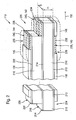
- FIG. 1 is a possible first embodiment of an implantable sensor 110 according to the invention for determining a glucose concentration in a body fluid.
- the implantable sensor 110 has an insulating carrier substrate 112, which in this embodiment consists of a non-conductive polyester.
- the insulating support substrate 112 has a height H of typically 0.8 to 1 millimeter, but other heights are possible, preferably heights in the range between 0.2 and 2 millimeters.
- the insulating carrier substrate, 112 has a width B which is in the range of one millimeter.
- an aspect ratio H / B of about 0.8.
- other widths B are possible, in particular widths between 0.3 millimeters and 2 millimeters.
- an aspect ratio which is in the range of 1.0, that is to say preferably of at least 0.3, whereby the inverse aspect ratio (ie 1 / k) should also be at least 0.3. This width of the aspect ratio ensures high stability of the implantable sensor 110.
- the insulating support substrate 112 is coated with a first electrode contact layer 114 and a second electrode contact layer 116 arranged on the opposite side.
- This may be, for example, a foil or another layer of a metal, such as, for example, gold, silver, platinum and / or aluminum, which is, for example, laminated onto the insulating carrier substrate 112.
- the electrode contact layers 114, 116 are applied over a large area onto the insulating carrier substrate 112, so that they extend over the full width B of the insulating carrier substrate 112.
- an insulator layer 118, 120 in the form of a self-adhesive film layer in this embodiment is applied to the electrode contact layers 114, 116.
- These insulator layers 118, 120 terminate at the left end of the implantable sensor 110 in FIG FIG. 1 in front of the end of the insulating support substrate 112, which in this area expose the first electrode contact layer 114 and the second electrode contact layer 116 and form electrical contacts 122, 124.
- the electrode contact layers 114, 116 can be electrically contacted, for example, by spring contacts are applied to these electrical contacts 122, 124 or by means of other contact means, such as electrical terminals or the like.
- the insulator layers 118, 120 have openings 126, 128.
- the upper opening 128 is configured in the form of a window, whereas the lower opening 126 is designed such that here the insulator layer 118 ends.
- Other embodiments of the openings 126, 128 are conceivable.
- a first electrode system 130 is introduced into the opening 126 and a second electrode system 132 is inserted into the opening 128 such that these electrode systems 130, 132 rest on the electrode contact layers 114, 116.
- the electrode systems 130, 132 thus form a first electrode 134 and a second electrode 136 in these areas together with the electrode contact layers 114, 116.
- the first electrode system 130 is composed of an Ag / AgCl coating
- second electrode system 132 is a MnO 2 / C (manganese dioxide) layer mixed with the enzyme glucose oxidase (GOD).
- GOD glucose oxidase
- the first electrode 134 functions as a common electrode 138 in this embodiment and performs the functions of counter electrode 140 and reference electrode 142.
- the second electrode 136 acts as a working electrode 144 in this embodiment.
- the implantable sensor in the region of the electrodes 134, 136 is enveloped by a membrane layer 146 made of polyurethane.
- This membrane layer 146 in this embodiment is impermeable to the enzyme glucose oxidase, but is at least partially permeable to glucose, for example, a diffusion of glucose through the membrane layer 146 can be inhibited. By means of this diffusion-inhibiting effect, for example, a current limitation can be realized.
- a layer structure could be realized in which only the working electrode 144, but not the counter electrode 140 and / or the reference electrode 142 are covered with the glucose diffusion-inhibiting membrane layer 146.
- the advantage of such an arrangement, in which only the working electrode 144 is covered with the membrane layer 146, is that this arrangement has a lower electrical resistance between the electrodes 140 and 142 and the surrounding electrolyte. Particularly in the case of the reference electrode 142, this reduced electrical resistance is manifested by an increased resistance to external electrical influences.
- the working electrode 144 could be coated with a membrane layer 146 which has diffusion inhibiting properties for glucose and impermeability to glucose oxidase, whereas the counter electrode 140 and the reference electrode 142 remain uncoated.
- the implantable sensor 110 (completely or partially, ie, for example in the region of the electrodes 140, 142, 144) could be coated with a further membrane layer 146, which has biocompatible properties, but no or only reduced diffusion-inhibiting properties and which only serves as outer protective layer ,
- the membrane layer 146 would be constructed in two layers in the region of the working electrode 146, whereas in the region of the counterelectrode 140 and the reference electrode 142, it would be single-layered.
- Other possibilities of the composition of the membrane layer 146 are conceivable.
- an insertion tip 148 is formed.
- This insertion tip 148 may, for example, be designed in one piece with the insulating carrier substrate 112 or it may also be an insertion tip 148 attached separately to the insulating carrier substrate 112.
- FIG. 3 schematically illustrates an apparatus 310 for determining a concentration of blood glucose using the sensor 110 according to the embodiment of FIG. 1 shown.
- the sensor 110 is symbolized here only symbolically by suggesting the working electrode 144 and the common electrode 138.
- the device 310 has a voltage measuring device 312, by means of which an electrochemical potential difference (voltage) between the working electrode 144 and the common electrode 138 can be measured.
- the device 310 has a current measuring device 314, by means of which a current flow between the working electrode 144 and the common electrode 138 can be measured.
- a control device 316 which controls the current flowing between the working electrode 144 and the common electrode 138 so that the voltage measured between the working electrode 144 and the common electrode 138 corresponds to a predetermined inching voltage.
- the control device 316 may for example have its own voltage source, which is variable. From the required settings of this additional voltage source of the control device 316 can then be closed, for example, on the electrochemical potential difference between the working electrode 144 and the common electrode 138.
- the components of the device 310 may be spatially separate.
- the sensor 110 may be partially or completely implanted in a body tissue, whereas the remainder of the device 310 may be located outside of the body tissue, for example, on the skin surface or in a separate device. From the Strommittnvornchtung 314 and the voltage measuring device 312 then lead corresponding lines to the electrical contacts 122, 124 of the sensor 110th
- FIG. 4 is an embodiment of a method according to the invention for producing a sensor 110 according to the in FIG. 1 illustrated embodiment illustrated. It should be pointed out, however, that other methods can also be used to design the implantable sensor 110 according to the invention as shown in FIG FIG. 1 manufacture. Also, the illustrated process steps need not necessarily be performed in the order given.
- a first method step 410 the electrode contact layers 114, 116 are applied over a large area to a carrier foil.
- the carrier film does not necessarily have to be identical to the insulating carrier substrates 112, since these insulating carrier substrates 112 are produced from the carrier film only by subsequent cutting (see below).
- both electrode contact layers 114, 116 and carrier film after performing this first process step 410 are still large, so that a large-area "sandwich" of a carrier film, embedded between two electrode contact layers 114, 116, is formed.
- the electrode contact layers also take their stripe shape thus only after cutting.
- metal foils which typically have layer thicknesses in the range of a few tens of micrometers.
- thinner or thicker layers are also conceivable, for example layer thicknesses in the range from a few tens to a few 100 nanometers using a vapor deposition or sputtering method or layer thicknesses in the region of 100 micrometers in roll-to-roll lamination processes.
- step 412 in FIG. 4 the insulator layers 118, 120 are applied.
- self-adhesive films are preferably used, which in turn are applied over a large area to the resulting after the implementation of step 410 sandwich structure.
- this self-adhesive film may be perforated or patterned from the outset, but an accurate positioning is usually not required, since the exact positioning of the openings 126, 128 is not critical in many cases.
- laminating methods are known to the person skilled in the art and can be used in a variety of ways.
- the openings 126, 128 can also be introduced subsequently, for example by subsequent cutting and removal of the insulator layers 118, 120.
- the first electrode system 130 is applied.
- an Ag / AgCl coating for applying this Ag / AgCl layer z.
- an Ag / AgCl paste which is formed for example by mixing silver and silver chloride particles with a solvent, by a printing process (eg screen printing, pad printing, stencil printing) and / or another coating method (eg. Squeezing, atomizing, in particular by slot nozzles, roll coating, o. ⁇ .) are introduced into the opening 126.
- the opening 126 is completely covered.
- Other printing methods can be used. It should be noted that the in FIG.
- first electrode system 130 may also overlap with the first insulator layer 118, which does not interfere with the functionality of the common electrode 138. An exact positioning is not required. Even the first insulator layer 118 may be co-coated over a wide area.
- the second electrode system 132 is applied.
- a mixture of manganese dioxide and glucose oxidase is used.
- the same method as in method step 414 can be used for application, for example a printing method and / or another coating method.
- Other methods are conceivable.
- a paste is used, which is solid after a corresponding drying and thus insoluble in the surrounding body fluid (electrolyte).
- a mixture of manganese dioxide and glucose oxidase it is also possible first of all to use a pure brownstone paste, onto which, for example, glucose oxidase is then dispensed by dehydration.
- the hitherto large-area layer structure is produced by a precision cutting method, whereby strips of width B (see FIG. 1 ) to arise. These strips have a longitudinal extent parallel to an insertion direction 150 (cf. FIG. 1 ). Precise positioning in precision cutting perpendicular to this insertion direction 150 is not required, in contrast to conventional methods using structured electrodes in the insertion direction 150 between which the cuts must be precisely positioned.
- the insertion tip 148 is molded onto the now formed insulating carrier substrates 112.
- insertion tips 148 may be created by simultaneous melting and drawing or may also be thermoformed accordingly.
- separate tips can be molded onto the insulating carrier substrates 112, for example by fusing them together with the insulating carrier substrates 112.
- this method step can also be omitted since, as mentioned above, the implantable sensor 110 can also be inserted into a separate insertion needle, for example. However, it is preferred if the sensor 110 has its own insertion tip 148, so that the electrodes 134, 136 are washed free of the body fluid (electrolyte).
- the membrane layer 146 is applied to the sensor 110.
- a simple immersion method in which the sensor 110 (without membrane layer) is immersed in a solution or another liquid containing the membrane material (or a precursor thereof).
- a uniform liquid film can optionally be additionally produced by spin coating, which is then dried can.
- a drying step is carried out in which the membrane layer 146 dries. A precise positioning of the dipping process is not necessary, since only the electrodes 134, 136 must be covered and an exceeding coverage of the sensor 110 is irrelevant to the measurement results.
- polyurethanes can be used as materials for the membrane layer 146.
- biocompatible materials should be used as membrane materials, that is to say materials which during the measurement period (typically one week, sometimes even more, plus a "safety time") do not react with the surrounding body tissue and / or the body fluid or significantly reduce toxic substances Give measurements.
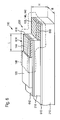
- FIG. 2 a second embodiment of an implantable sensor 110 according to the invention is shown, wherein in this embodiment, the insertion tip 148 is not shown or omitted.
- the sensor 110 according to the embodiment in FIG. 2 has a first insulating carrier substrate 210 embedded between a first electrode contact layer 212 and a second electrode contact layer 214.
- the second electrode contact layer 214 is adjoined by a second insulating carrier substrate 216, which, however, does not extend over the entire longitudinal extent of the first insulating carrier substrate 210.
- a region of the second electrode contact layer 214 is left uncovered at the left end of the sensor 110 (that is, opposite to the insertion direction 150), so that an electrical contact for contacting the second electrode contact layer 214 forms there (for contacting: see above).
- the second insulating carrier substrate 216 ends in front of the first insulating carrier substrate 210, so that a step 220 is formed in this region. It should be noted here that alternatively, this stage 220 instead of "up” as in FIG. 2 can also be designed “down", so that a total of an inversion of the layer structure is possible.
- the second insulating carrier substrate 216 is coated with a third electrode contact layer 222.
- all the electrode contact layers 212, 214, 222 extend over the entire width B of the sensor 110.
- materials for the electrode contact layers 212, 214, 222 basically the same materials can be used as in the case of FIG. 1 ,
- the sensor 110 Insulated on the outside with insulator layers 118, 120, which in this case, the first electrode contact layer 212 and the third electrode contact layer 222 on the outside electrically against the surrounding electrolyte, in particular the body fluid, isolate. Again, these may be self-adhesive foils.
- the insulators 118, 120 at the left end of the sensor 110 before the end of the associated insulating support substrates 210 and 216, respectively, such that electrical contacts 224, 226 remain free, via which the electrode contact layers 212 and 222 can be electrically contacted.
- Openings 228, 230 provided in the insulator layers 118 and 120 are also in the embodiment according to FIG. 2 Openings 228, 230 provided in the insulator layers 118 and 120. These openings 228, 230, which in turn may be formed, for example, as "windows" and / or as simple remaining regions of the electrode contact layers 212, 222, can in turn already be produced during the application of the insulator layers 118, 120 or can be produced by subsequent structuring.
- a first electrode system 232, a second electrode system 234 and a third electrode system 236 are applied.
- the first electrode system 232 and second electrode system 234 again, as in the embodiment according to FIG. 1 , used of an Ag / AgCl layer.
- a third electrode system 232 a manganese dioxide GOD layer is again used, analogous to the second electrode system 132 in FIG FIG. 1 , Together with the associated electrode contact layers 212, 214 and 222, these electrode systems 232, 234, 236 then each form a first electrode 238, a second electrode 240 and a third electrode 242.
- the first electrode 238 acts in this embodiment as a counter electrode 140, the second Electrode 240 as a reference electrode 142 and the third electrode 242 as a working electrode 144.
- the three electrodes 238, 240, 242 are all arranged in different layer planes of the layer structure.
- these electrodes can be made very wide (that is, in this case over the full width B), but are nevertheless reliably separated from each other.
- the senor 110 in the region of the electrodes 238, 240, 242 is, as in FIG. 1, still surrounded by a membrane layer 146 which, analogous to the exemplary embodiment in FIG FIG. 1 can be designed.
- FIG. 3B is a device 310 for determining a blood glucose concentration using a sensor 110 according to the in FIG. 1 illustrated embodiment illustrated.
- the three electrodes 140, 144, 142 are configured as separate electrodes. All three electrodes are again lapped by the electrolyte of the body fluid.
- the working electrode 144 which in turn has glucose oxidase, again a conversion of glucose into gluconolactone to form electrons fed.
- the electrochemical potential of the working electrode 144 is again determined by the concentration of glucose in the body fluid.
- the device 310 comprises a voltage measuring device 312 for the voltage between the working electrode 144 and the reference electrode 142, and a current measuring device 314 for measuring a current flowing between the counter electrode 140 and the working electrode 144. Furthermore, a control device 316 is again provided, which regulates the current flowing between the counter electrode 140 and the working electrode 144 in such a way that the voltage between the working electrode 144 and the reference electrode 142 reaches a predetermined desired value. Incidentally, the method works as described by FIG. 3A described.
- FIG. 5 is finally an inventive embodiment of a manufacturing method for producing a sensor 110 according to the embodiment in FIG. 2 shown.
- a manufacturing method for producing a sensor 110 according to the embodiment in FIG. 2 shown.
- other manufacturing methods for producing this sensor 110 can be used.
- the Process steps are performed in a different sequence of Rhine, and it can also be carried out in turn, additional process steps, not shown.
- the method is in FIG. 5 divided into two sub-processes, in which a first sub-layer structure (sub-process 510) and a second sub-layer structure (sub-process 512) are produced independently. Subsequently, in the common method 514, the two sub-layer structures are joined together and further processed.
- step 516 a first carrier film over a large area with the electrode contact layers 212, 214 coated.
- step 518 the insulator film 118 is applied to the first electrode contact layer 212, analogously to method step 412 according to FIG FIG. 4 , but only one-sided.
- step 520 the first electrode system 232 is introduced into the opening 228 in the insulator layer 118, for example by means of FIG FIG. 4 described method.
- the second electrode system 234 is applied to a region of the second electrode contact layer 214 in which the step 220 is later formed.
- the second electrode system 234 can also be applied, for example, only in the context of the common method 514, that is to say after joining the two sub-layer structures (see below).
- the first sub-layer structure is ready.
- a second sub-layer structure is produced.
- a second carrier film is coated over a large area and on one side with the third electrode contact layer 222.
- the insulator layer 120 is applied to the third electrode contact layer 222, wherein an opening 230 remains.
- the third electrode system 236 is introduced into the opening 230.
- the second sub-process 512 is completed, and the second sub-layer structure is made.
- the second sub-layer structure which is composed of the second carrier film, the third electrode substrate layer 222, the insulator layer 120 and the third electrode system 236, is applied to the first sub-layer structure, which consists of the insulator layer 118, of the first electrode contact layer 212, the first carrier foil, the second electrode contact layer 214, and the first electrode system 232 and the second electrode system 234.
- laminating techniques may be used for this application.
- step 532 again a precision cutting takes place in which the previously large-area layer structures are cut into strip-shaped sensors 110. Again, here is as described above; exact positioning is not essential.
- an insertion tip 148 is optionally integrally formed on the layer structure, which in the illustration according to FIG. 2 not shown.
- step 536 the membrane layer 146 is applied, analogously to method step 422, for example again by a dipping method.
- Illustrated exemplary method for producing the sensors 110 can be realized well on a large scale.
- roll-to-roll methods can be used for which machines from other areas of technology are available, so that no custom-made production equipment is required.
- the process is extremely cost effective and can be run with high yield and high throughput.
- FIGS. 6 to 8 Further advantageous embodiments of implantable sensors 110 are shown. So shows FIG. 6 an embodiment of an implantable sensor 110 shown in a stepped arrangement.
- the implantable sensor 110 has a first insulating carrier substrate 210 on which a first electrode contact layer 610 is applied.
- this first insulating carrier substrate 210 have a layer thickness of about 200 microns.
- a first electrode contact layer 610 is applied to this first insulating carrier substrate 210, analogously to the preceding exemplary embodiments, which again may be, for example, a gold layer or a layer of another metal or conductive polymer.
- This first electrode contact layer has, for example, a layer thickness of a few ⁇ m.
- a second insulating carrier substrate 216 is applied, which may be configured analogously to the first insulating carrier substrate 210.
- the second insulating carrier substrate 216 extends on the electrode side, ie on the right in FIG. 6 , not over the entire length of the first insulating carrier substrate 210, so that a step 220 is formed in this area.
- a second electrode contact layer 612 is applied, which may be configured analogously to the first electrode contact layer 610.
- an insulator layer 120 is applied, for example, an adhesive tape, analogous to the preceding embodiments.
- This insulator layer 120 extends on the electrode side (ie in turn on the right side of the implantable sensor 110 in FIG. 6 ) not over the entire length of the second insulating carrier substrate 216 and the second electrode contact layer 612, so that in turn, analogous to the opening 230 in FIG. 2 , an opening 614 remains, that is, a region in which the second electrode contact layer 612 is not covered by the insulator layer 120.
- the second electrode contact layer 612 is covered with a first electrode system 616, which, as in the case of the second electrode system 132 in FIG. 1 is an MnO 2 / C (manganese dioxide) layer mixed with GOD.
- a working electrode 144 thus forms in the region of the opening 614.
- the first electrode contact layer 610 which is not covered by the second insulating carrier substrate 216 in the region of the step 220, is covered in this region by a second electrode system 618, which is analogous to the first electrode system 130 according to the exemplary embodiment in FIG. 1 can be designed.
- the second electrode system 618 may once again be an Ag / AgCl coating.
- Electrode 138 which performs the functions of counter electrode 140 and reference electrode 142.
- Working electrode 144 and common electrode 138 are in turn covered by a membrane layer 146, analogous to the previous embodiments.
- the embodiment of the implantable sensor 110 according to FIG. 6 thus, a mixed form of the embodiments according to the FIGS. 1 and 2
- a stage arrangement according to the embodiment in FIG. 2 provided, in which both electrodes 144, 138 are arranged in parallel and with their free electrode surfaces in the same direction (in the embodiment of FIG. 6 up).
- the counter electrode 140 and the reference electrode 142 are designed as a common electrode 138, analogous to the exemplary embodiment in FIG. 1
- the width B of the implantable sensor 110 according to the embodiment in FIG. 6 is typically about 1 mm. This results, taking into account a height H of the insulating carrier substrates 210 and 216, an aspect ratio of about 0.4.
- the electrodes 144, 138 have a length L of typically about 1 mm.
- FIG. 7 a further embodiment of an implantable sensor 110 is shown, which in turn is a modification of the embodiment according to FIG. 2 represents.
- the implantable sensor 110 according to FIG. 7 has three insulating carrier substrates 710, 712 and 714, which in turn are covered by associated electrode contact layers 716, 718 and 720.
- the second insulating carrier substrate 712 and the second electrode contact layer 718 are applied to the first insulating carrier substrate 710 and the first electrode contact layer 716 such that a first opening 722 remains and a first step 724 forms.
- the third insulating carrier substrate 714 and the third electrode contact layer 720 are applied to the second insulating carrier substrate 712 and the second electrode contact layer 718 to form a second opening 726 and a second stage 728.
- an insulator layer 120 is applied to the third electrode contact layer 720, which in turn does not extend completely to the electrode-side end of the third electrode contact layer 720, so that a third opening 730 remains.
- the electrode contact layers 716, 718 and 720 are each covered with electrode systems 732, 734 and 736.
- the second electrode system 734 again comprises an MmO 2 / C (manganese dioxide) layer. Accordingly, a reference electrode 738, a working electrode 740 and a counter electrode 742 are formed in the different ones Layer planes of the "staircase construction" according to FIG. 7 out.
- the layer structure of the embodiment of the implantable sensor 110 according to FIG. 7 basically the layer structure in FIG. 2 , but with the difference that all the electrodes 738, 740, 742 point in one direction with their electrode surfaces.
- the working electrode 740 is thereby "framed" between the reference electrode 738 and the counter-electrode 742.
- the electrodes 738, 740, 742 are enveloped by a membrane layer 146.
- the layer thicknesses of the insulating carrier substrates 710, 712, 714 correspond to the layer thickness H of the insulating carrier substrate 210 according to FIG. 6 , amount to about 200 microns.
- the electrode contact layers 716, 718 and 720 have a thickness of about 50 microns, as well as the electrode systems 732, 734 and 736.
- the length L of the individual openings 722, 726 and 730 is again about 1 mm.
- FIG. 8 a further embodiment of an implantable sensor 110 is shown, which properties of the implantable sensors according to the embodiments in the FIGS. 6 and 7 united. So are, analogous to FIG. 6 , again two insulating carrier substrates 810 and 812 are provided. However, unlike the first insulating carrier substrate 810 FIG. 6 , not a single electrode contact layer, but two electrode contact layers 814 and 816 are applied, each occupying approximately half the width B of the first insulating support substrate 810 and extending along the length of this first insulating support substrate 810.
- both electrode contact layers 814, 816 can also be applied directly, ie already electrically insulated from one another, to the first insulating carrier substrate 810.
- the second insulating carrier substrate 812 is in turn applied to the two electrode contact layers 814, 816 or the first insulating carrier substrate 810 in such a way that at the electrode-side end (right in FIG. 8 ), a first opening 818 remains and a step 820 forms.
- a third electrode contact layer 822 is applied, which in turn, analogous to FIG. 6 , is covered by an insulator layer 120 such that at the electrode end (right in FIG. 8 ) a second opening 824 remains.
- the first electrode contact layer 814 is covered with a first electrode system 826
- the second electrode contact layer 816 is covered with a second electrode system 828.
- Both electrode systems 826, 828 are analogous to the second electrode system 618 in FIG. 6 to Ag / AgCl coatings.
- a counter electrode 830 and a reference electrode 832 forms, which in turn, for example, in a device 310 according to the embodiment in FIG. 3B can be used.
- an MnO 2 / C (manganese dioxide) layer is again applied as a third electrode system 834 to the third electrode contact layer 822, so that a working electrode 836 is formed here.
- the embodiment of the implantable sensor 110 according to FIG. 8 In principle, a similar "1-step structure" too FIG. 6
- counter electrode 830 and reference electrode 832 are located separately in a plane of the layer structure.
- a device 310 according to FIG. 3B whereas, for the embodiment of the implantable sensor 110, for example, a device 310 according to the exemplary embodiment in FIG FIG. 3A could be used.
- a device 310 according to the exemplary embodiment in FIG. 3A could be used.
- the device 310 according to the embodiment in FIG. 3B deploy.
- Analogous to the embodiments in the FIGS. 6 and 7 is also in the embodiment according to FIG. 8 the implantable sensor 110 in the region of the electrodes 830, 832 and 836 again completely or partially covered with a membrane layer 146. All three embodiments according to the FIGS. 6 to 8 is common that all electrodes with their large electrode surface are parallel (albeit in different layer planes) and point in the same direction.
Abstract
Description
Es wird ein implantierbarer Sensor zur Ermittlung einer Konzentration mindestens eines Analyten in einem Medium, insbesondere einem Körpergewebe und/oder einer Körperflüssigkeit, eine Vorrichtung, welche den implantierbaren Sensor verwendet, sowie ein Verfahren zur Herstellung des implantierbaren Sensors vorgeschlagen. Derartige Sensoren und/oder Vorrichtungen werden insbesondere im Bereich der Medizintechnik eingesetzt, beispielsweise um elektrochemisch eine Konzentration von Blutglucose, Triglyceriden, Laktat oder anderer Analyten zu bestimmen.An implantable sensor is proposed for determining a concentration of at least one analyte in a medium, in particular a body tissue and / or a body fluid, a device which uses the implantable sensor, and a method for producing the implantable sensor. Such sensors and / or devices are used in particular in the field of medical technology, for example, to determine electrochemically a concentration of blood glucose, triglycerides, lactate or other analytes.
Die Bestimmung der Blutglucosekonzentrationen sowie eine entsprechende Medikation ist für Diabetiker ein essentieller Bestandteil des Tagesablaufs. Dabei muss die Blutglucosekonzentration schnell und einfach mehrmals am Tag (typischerweise zwei bis sieben Mal) bestimmt werden, um gegebenenfalls entsprechende medizinische Maßnahmen ergreifen zu können. In vielen Fällen erfolgt dabei eine Medikation mittels automatischer Systeme, insbesondere so genannte Insulinpumpen.The determination of the blood glucose concentrations and a corresponding medication is an essential part of the daily routine for diabetics. The blood glucose concentration must be determined quickly and easily several times a day (typically two to seven times) in order to be able to take appropriate medical measures if necessary. In many cases, medication is thereby carried out by means of automatic systems, in particular so-called insulin pumps.
Um den Tagesablauf des Diabetikers nicht mehr als nötig einzuschränken, werden häufig entsprechend mobile Geräte eingesetzt, welche einfach zu transportieren und zu handhaben sein sollten, so dass eine Messung der Blutglucosekonzentration, beispielsweise am Arbeitsplatz oder auch in der Freizeit, problemlos erfolgen kann. Derzeit sind verschiedene mobile Geräte am Markt, welche teilweise nach unterschiedlichen Messmethoden und unter Verwendung unterschiedlicher Diagnoseverfahren funktionieren. Ein erstes Messverfahren beruht beispielsweise auf einer elektrochemischen Messmethode, wobei eine Blutprobe, welche vom Patienten beispielsweise durch Perforieren einer Hautschicht mittels einer Lanzette dem Körpergewebe entnommen wird, auf eine mit Enzymen und Mediatoren beschichtete Elektrode appliziert wird. Entsprechende Teststreifen für derartige elektrochemische Messverfahren sind beispielsweise in
Die beschriebenen Nachweisverfahren beruhen also überwiegend darauf, dass ein Patient zunächst eine entsprechende Probe der zu untersuchenden Körperflüssigkeit entnimmt (wobei es sich beispielsweise um eine Blutprobe oder eine Urinprobe handelt) und diese dann entsprechend mittels der Testvorrichtung untersucht. Dieses Verfahren beinhaltet jedoch verschiedene Nachteile. So ist zum einem dieses Verfahren äußerst aufwändig und setzt mehrere Handhabungsschritte voraus. So muss beispielsweise eine Lanzette bereitgestellt und gespannt werden, anschließend mittels dieser Lanzette eine Hautschicht perforiert werden, dann ein so erzeugter Blutstropfen auf einen Teststreifen aufgetragen werden und anschließend dieser Teststreifen mittels eines entsprechenden Gerätes ausgewertet werden. Für viele Patienten, insbesondere ältere Menschen und Kinder, sind diese Handhabungsschritte oftmals nur schwer durchzuführen, da die Patienten beispielsweise in ihrer motorischen Fähigkeit und ihrem Sehvermögen eingeschränkt sind. Weiterhin lassen sich diese Verfahrensschritte nur in wenigen Fällen diskret durchführen, so dass beispielsweise ein Schutz der Privatsphäre des Patienten bei einer Messung am Arbeitsplatz nur unzureichend gewahrt ist. Auch kann eine Fehlbedienung des Messverfahrens leicht zu falschen Messwerten führen, mit teilweise fatalen Folgen einer auf den Messergebnissen aufbauenden falschen Medikation.Thus, the described detection methods are predominantly based on the fact that a patient first extracts a corresponding sample of the body fluid to be examined (which is, for example, a blood sample or a urine sample) and then examines it accordingly by means of the test device. However, this method involves several disadvantages. On the one hand, this process is extremely complex and requires several handling steps. Thus, for example, a lancet must be provided and tensioned, then a skin layer is perforated by means of this lancet, then a blood drop produced in this way can be applied to a test strip and then this test strip can be evaluated by means of a corresponding device. For many patients, especially the elderly and children, these manipulations are often difficult to accomplish because patients are limited in their motor ability and vision, for example. Furthermore, these method steps can be carried out discretely only in a few cases, so that, for example, a protection of the privacy of the patient in a measurement at the workplace is insufficiently preserved. Also, a misuse of the measurement method can easily lead to false readings, with sometimes fatal consequences of a build-up on the measurement results wrong medication.
Aus dem Stand der Technik sind daher Systeme bekannt, welche in ein Körpergewebe implantiert werden können und welche beispielsweise kontinuierlich Messwerte liefern. So offenbart beispielsweise
Auch
Insgesamt sind jedoch die aus dem Stand der Technik bekannten implantierbaren Sensoren bezüglich ihres Aufbaus und ihrer Herstellung äußerst aufwendig. Geht man davon aus, dass es sich bei diesen Sensoren um nur für kurze Zeit (typischerweise circa eine Woche) verwendbare Einwegsensoren handelt, so wird deutlich, dass die bei den aus dem Stand der Technik bekannten Sensoren eingesetzten Verfahren derartigen Anforderungen an Einwegartikel nicht gerecht werden.Overall, however, the known from the prior art implantable sensors are extremely expensive in terms of their structure and their production. Assuming that these sensors are disposable sensors that can be used only for a short time (typically about one week), it becomes clear that the methods used in the sensors known from the prior art do not meet such requirements for disposable items ,
So ist beispielsweise für die Herstellung des aus
Auch sind lithographische Verfahren, insbesondere das mit diesen Verfahren verbundene Ätzen von Metallschichten, nicht immer so zuverlässig, wie dies für die Herstellung medizintechnischer Produkte erforderlich ist. Insbesondere kann es vorkommen, dass einzelne Elektroden noch durch "Brücken" miteinander verbunden sind, so dass die Funktionalität der Sensoren aufgrund von Herstellungsproblemen leicht beeinträchtig oder sogar ganz verhindert sein kann. Ein weiterer Nachteil der aus dem Stand der Technik bekannten Sensoren, wie beispielsweise der aus der
In
Die in
Dokumente
Aufgabe der Erfindung ist es somit, einen Sensor zur Ermittlung einer Konzentration mindestens eines Analyten in einem Medium zur Verfügung zu stellen, welcher einfach und kostengünstig mittels eines zuverlässigen Herstellungsverfahrens herstellbar ist und welcher die Nachteile der aus dem Stand der Technik bekannten Sensoren und Verfahren nach Möglichkeit vermeidet. Insbesondere soll der Sensor implantierbar sein und ausreichende Signalhübe gewährleisten.The object of the invention is therefore to provide a sensor for determining a concentration of at least one analyte in a medium which can be produced easily and inexpensively by means of a reliable production method and which detects the disadvantages of the sensors and methods known from the prior art Possibility avoids. In particular, the sensor should be implantable and ensure sufficient signal strokes.
Diese Aufgabe wird durch die Erfindung mit den Merkmalen der unabhängigen Ansprüche gelöst. Vorteilhafte Weiterbildungen der Erfindung sind in den Unteransprüchen gekennzeichnet. Der Wortlaut sämtlicher Ansprüche wird hiermit durch Bezugnahme zum Inhalt der Beschreibung gemacht.This object is achieved by the invention with the features of the independent claims. Advantageous developments of the invention are characterized in the subclaims. The wording of all claims is hereby incorporated by reference into the content of the description.
Es wird ein implantierbarer Sensor zur Ermittlung einer Konzentration mindestens eines Analyten in einem Medium, insbesondere in einem Körpergewebe und/oder einer Körperflüssigkeit, vorgeschlagen. Bei dem Analyten kann es sich beispielsweise um Glucose, Triglyceride, Laktat, Hormone oder andere Analyten handeln, welche insbesondere in der Medizin eine Rolle spielen. Alternativ oder zusätzlich kann der Sensor jedoch auch zur Messung anderer Arten von Analyten eingesetzt werden. Insbesondere beruht der Sensor auf der Verwendung eines elektrochemischen Messverfahrens.An implantable sensor for determining a concentration of at least one analyte in a medium, in particular in a body tissue and / or a body fluid, is proposed. The analyte may be, for example, glucose, triglycerides, lactate, hormones or other analytes, which play a role in particular in medicine. Alternatively or additionally, however, the sensor can also be used to measure other types of analytes. In particular, the sensor is based on the use of an electrochemical measuring method.
Ein Grundgedanke der Erfindung besteht darin, die oben beschriebene Problematik, dass einerseits eine elektrische Isolierung der Elektroden gegeneinander erforderlich ist und andererseits die Elektroden für den mindestens einen Analyten möglichst frei zugänglich sein sollten, durch einen geeigneten Schichtaufbau zu lösen. Dementsprechend wird ein implantierbarer Sensor derart ausgestaltet, dass mindestens zwei Elektroden auf einem elektrisch isolierenden Trägersubstrat in mindestens zwei verschiedenen Schichtebenen, beispielsweise auf einer Vorder- und einer Rückseite und/oder in verschiedenen Stufenebenen, aufgebracht werden. Die mindestens zwei Elektroden sind durch das mindestens eine Trägersubstrat elektrisch voneinander getrennt.A basic idea of the invention consists of solving the problem described above, namely that electrical insulation of the electrodes against each other is required and that the electrodes for the at least one analyte should be as freely accessible as possible through a suitable layer structure. Accordingly, an implantable sensor is configured in such a way that at least two electrodes are applied to an electrically insulating carrier substrate in at least two different layer planes, for example on a front and a rear side and / or in different step levels. The at least two electrodes are electrically separated from one another by the at least one carrier substrate.
Weiterhin weisen die mindestens zwei Elektroden Elektrodenflächen auf, also aktive Oberflächen, an denen elektrochemische Reaktionen (Redoxreaktionen) ablaufen können. Diese mindestens zwei Elektrodenflächen sind erfindungsgemäß, um einen maximalen Signalhub zu erzielen, bei in das Medium implantiertem Sensor dem Medium zugewandt und stehen unmittelbar oder über eine Analyt-durchlässige Membranschicht im Wesentlichen gleichförmig mit dem Medium in Kontakt. Dies bedeutet insbesondere, dass nicht nur, wie in
Durch die erfindungsgemäße Ausgestaltung wurden also die beiden Funktionen, welche in
Der implantierbare Sensor kann auf verschiedene Arten vorteilhaft erfindungsgemäß weitergebildet werden. Die beschriebenen vorteilhaften Weiterbildungen können dabei einzeln oder in Kombination verwendet werden.The implantable sensor can advantageously be further developed according to the invention in various ways. The described advantageous developments can be used individually or in combination.
Vorzugsweise umfassen die mindestens zwei Elektroden mindestens eine Arbeitselektrode und mindestens eine weitere Elektrode, insbesondere mindestens eine Gegenelektrode und/oder mindestens eine Referenzelektrode. Dabei sind vorzugsweise die mindestens eine Arbeitselektrode und die mindestens eine weitere Elektrode in unterschiedlichen Schichtebenen des Schichtaufbaus angeordnet. Die Messung der Analytkonzentration erfolgt dann vorzugsweise nach Benetzung durch das Medium bzw. nach Implantierung des Sensors durch amperometrische Messung zwischen den mindestens zwei Elektroden (Arbeits- und Gegenelektrode), insbesondere mittels einer Gleichspannung. Eine Referenzelektrode zur stromlosen Messung des Arbeitselektrodenpotenzials kann zusätzlich verwendet werden.Preferably, the at least two electrodes comprise at least one working electrode and at least one further electrode, in particular at least one counterelectrode and / or at least one reference electrode. In this case, the at least one working electrode and the at least one further electrode are preferably in different layer planes arranged the layer structure. The analyte concentration is then preferably measured after wetting through the medium or after implantation of the sensor by amperometric measurement between the at least two electrodes (working and counterelectrode), in particular by means of a DC voltage. A reference electrode for electroless measurement of the working electrode potential may additionally be used.
Unter "in unterschiedlichen Schichtebenen" soll dabei insbesondere zu verstehen sein, dass zwischen den mindestens zwei Elektroden mindestens ein isolierendes Trägersubstrat angeordnet ist, so dass mindestens zwei der mindestens zwei Elektroden durch das isolierende Trägersubstrat getrennt sind. Somit wird, im Gegensatz zum oben beschriebenen Stand der Technik, bei diesem Aufbau eines implantierbaren Sensors die "dritte Dimension" mitgenutzt.By "in different layer planes" is to be understood in particular that at least one insulating carrier substrate is arranged between the at least two electrodes, so that at least two of the at least two electrodes are separated by the insulating carrier substrate. Thus, in contrast to the above-described prior art, in this structure of an implantable sensor, the "third dimension" is shared.
Zwar sind aus dem Stand der Technik elektrochemische Zellen, beispielsweise elektrochemische Mikrozellen, bekannt, bei welchen Elektroden auf gegenüberliegenden Seiten eines Trägers angeordnet sind. In diesem Fall handelt es sich jedoch bei dem Träger regelmäßig um ein Elektrolytmaterial, insbesondere einen Feststoffelektrolyten. Im Gegensatz dazu weist das mindestens eine isolierende Trägersubstrat des erfindungsgemäßen elektrochemischen Sensors ein elektrisch nicht leitendes Material auf. Dies soll insbesondere bedeuten, dass, wenn an zwei auf entgegengesetzten Seiten des mindestens einen isolierenden Trägersubstrats angeordnete Elektroden eine Spannung von bis zu ca. 1-2 Volt angelegt wird, Ströme von nicht mehr als einem Milliampere, vorzugsweise von nicht mehr 100 Mikroampère, und besonders bevorzugt von nicht mehr als 10 Mikroampère, fließen. Dadurch ist gewährleistet, das der Messstrom aufgrund des elektrochemischen Messverfahrens erheblich größer ist als der Strom, welcher trotz der isolierenden Eigenschaften des elektrisch nicht leitenden Materials des mindestens einen isolierenden Trägersubstrats durch das mindestens eine isolierende Trägersubstrat fließt.Although known from the prior art electrochemical cells, such as electrochemical microcells, are known, in which electrodes are arranged on opposite sides of a carrier. In this case, however, the carrier is usually an electrolyte material, in particular a solid electrolyte. In contrast, the at least one insulating carrier substrate of the electrochemical sensor according to the invention has an electrically non-conductive material. This is intended in particular to mean that, when a voltage of up to approximately 1-2 volts is applied to two electrodes arranged on opposite sides of the at least one insulating carrier substrate, currents of not more than one milliampere, preferably not more than 100 microamps, and most preferably no more than 10 microamps, flow. This ensures that the measuring current due to the electrochemical measuring method is considerably greater than the current which, despite the insulating properties of the electrically non-conductive material of the at least one insulating carrier substrate, flows through the at least one insulating carrier substrate.
Weiterhin kann das mindestens eine Trägersubstrat auch zusätzlich derart ausgestaltet sein, dass eine Diffusion des mindestens einen Analyten durch das mindestens eine Trägersubstrat nicht möglich oder stark behindert ist. Insofern unterscheidet sich das mindestens eine Trägersubstrat hinsichtlich der Materialanforderungen deutlich auch von der in
Zur Kontaktierung der mindestens zwei Elektroden kann der implantierbare Sensor weiterhin eine oder mehrere Elektrodenkontaktschichten aufweisen. Dabei kann sich beispielsweise um elektrisch leitende Schichten handeln, z. B. metallische Schichten, insbesondere um Schichten, welche Karbon, Graphit, Gold, Silber, Platin, und/oder Aluminium aufweisen. Auch mehrschichtige Aufbauten sind möglich. Auch organische Leitermaterialien kommen als elektrisch kontaktierende Elektrodenkontaktschichten in Betracht.For contacting the at least two electrodes, the implantable sensor may further comprise one or more electrode contact layers. This may be, for example, electrically conductive layers, for. For example, metallic layers, in particular layers, which include carbon, graphite, gold, silver, platinum, and / or aluminum. Also multi-layered structures are possible. Organic conductor materials are also suitable as electrically contacting electrode contact layers.
Da die mindestens zwei Elektroden in mindestens zwei Schichtebenen des Schichtaufbaus des Sensors angeordnet sind, ist es nunmehr möglich, dass sich die mindestens zwei Elektroden und/oder die mindestens zwei Elektrodenkontaktschichten im Wesentlichen über die gesamte Breite des mindestens einen isolierenden Trägersubstrats erstrecken. So kann das isolierende Trägersubstrat insbesondere eine Längserstreckung sowie eine Breite und eine Länge aufweisen, wobei sich die Elektrodenkontaktschichten und/oder die Elektroden im Wesentlichen in einem Rand des isolierenden Trägersubstrats zum anderen erstrecken. Unter "im Wesentlichen" kann dabei eine Abdeckung des isolierenden Trägersubstrats durch die Elektrodenkontaktschicht von mindestens 80%, vorzugsweise 95% und besonders bevorzugt von 100% verstanden werden. Eine Strukturierung der Elektroden und/oder Elektrodenkontaktschichten ist also aufgrund der Trennung durch den Aufbau in verschiedenen Ebenen nicht mehr erforderlich, so dass auf aufwändig lithographische Strukturierungsverfahren oder Laserstrukturierungsverfahren (z. B. Laserablation) verzichten werden kann. Die Vorteile dieser Möglichkeit werden unten deutlich, wenn ein mögliches Herstellungsverfahren des implantierbaren Sensors im Detail beschrieben wird.Since the at least two electrodes are arranged in at least two layer planes of the layer structure of the sensor, it is now possible for the at least two electrodes and / or the at least two electrode contact layers to extend over substantially the entire width of the at least one insulating carrier substrate. Thus, the insulating carrier substrate may in particular have a longitudinal extent and a width and a length, wherein the electrode contact layers and / or the electrodes extend substantially in one edge of the insulating carrier substrate to the other. By "substantially", a coverage of the insulating carrier substrate by the electrode contact layer of at least 80%, preferably 95% and particularly preferably 100% can be understood. A structuring of the electrodes and / or electrode contact layers is therefore no longer required due to the separation by the structure in different planes, so that can be dispensed with elaborate lithographic patterning or laser structuring method (eg. The advantages of this approach will become apparent below when describing in detail one possible method of manufacturing the implantable sensor.
Weiterhin kann der implantierbare Sensor mindestens eine Isolatorschicht aufweisen, welche die mindestens zwei Elektrodenkontaktschichten zumindest teilweise, vorzugsweise jedoch vollständig, gegen das Medium, insbesondere das Körpergewebe und/oder die Körperflüssigkeit, abdeckt und vorzugsweise elektrisch isoliert. Dabei können die beispielsweise mindestens zwei Elektrodenkontaktschichten teilweise von den mindestens zwei Elektroden bedeckt sein, wobei die unbedeckten Bereiche (z. B. nachträglich) durch die mindestens eine Isolatorschicht bedeckt werden. Vorzugweise werden als Isolatorschichten selbstklebende Folienschichten eingesetzt. Auf diese Weise wird beispielsweise durch die mindestens eine Isolatorschicht verhindert, dass an den unbedeckten Bereichen der Elektrodenkontaktschichten bei Kontakt mit dem umgebenden Medium und Anlegen einer Spannung unerwünschte elektrochemische Reaktionen, beispielsweise Elektrolysereaktionen unter Gasbildung, ablaufen.Furthermore, the implantable sensor can have at least one insulator layer which covers the at least two electrode contact layers at least partially, but preferably completely, against the medium, in particular the body tissue and / or the body fluid, and preferably electrically insulates. In this case, the at least two electrode contact layers, for example, may be partially covered by the at least two electrodes, the uncovered regions (eg, subsequently) being covered by the at least one insulator layer. Preferably, self-adhesive film layers are used as insulator layers. In this way, it is prevented, for example by the at least one insulator layer, that unwanted electrochemical reactions, for example electrolysis reactions with formation of gas, take place at the uncovered regions of the electrode contact layers upon contact with the surrounding medium and application of a voltage.
Neben dem oben beschriebenen Schichtaufbau können auch noch weitere, nicht genannte Schichten vorgesehen sein. So kann es sich bei dem mindestens einen isolierenden Trägersubstrat zunächst um ein Trägersubstrat aus beispielsweise einem Kunststoff-, Keramik- oder Papiermaterial handeln. Alternativ oder zusätzlich kann das mindestens eine Trägersubstrat selbst bereits um einen mehrschichtigen Aufbau aufweisen, beispielsweise ein Substratmaterial, welches mit weiteren Schichten besichtet ist. So können beispielsweise Substratmaterialen mit zusätzlichen Barriereschichten eingesetzt werden. Besonders bevorzugt ist es, wenn das mindestens eine isolierende Trägersubstrat als Werkstoff ein Polymer, ein isolierendes Polymer, vorzugsweise einen Polyester, aufweist. Zwischen den mindestens einen isolierenden Trägersubstrat und die mindestens zwei Elektrodenkontaktschichten und/oder die mindestens zwei Elektroden können auch weitere Schichten eingebracht sein, beispielsweise leitende oder elektrisch isolierende Schichten.In addition to the layer structure described above, further, not mentioned, layers can also be provided. Thus, the at least one insulating carrier substrate may initially be a carrier substrate of, for example, a plastic, ceramic or paper material. Alternatively or additionally, the at least one carrier substrate itself may already have a multi-layered structure, for example a substrate material, which is coated with further layers. For example, substrate materials with additional barrier layers can be used. It is particularly preferred if the at least one insulating carrier substrate has as its material a polymer, an insulating polymer, preferably a polyester. Between the at least one insulating carrier substrate and the at least two electrode contact layers and / or the at least two electrodes, it is also possible to introduce further layers, for example conductive or electrically insulating layers.
Der implantierbare Sensor gemäß der obigen Beschreibung kann beispielsweise in eine Kanüle, wie aus dem Stand der Technik bekannt, eingesetzt werden. Besonders bevorzugt ist es jedoch, wenn der implantierbare Sensor unmittelbar, das heißt ohne umgebende Kanüle oder Kapillare in das Medium insbesondere das Körpergewerbe, eingebracht werden kann. Auf diese Weise ist gewährleistet, dass die in den mindestens zwei Ebenen angeordneten Elektroden frei von Körperflüssigkeit umspült werden können. Zu diesem Zweck kann der implantierbare Sensor, wie oben bereits beschrieben, mindestens eine den Schichtaufbau ganz oder teilweise umschließende Membranschicht aufweisen. Vorteilhafterweise weist diese mindestens eine Membranschicht zumindest teilweise eine Durchlässigkeit für den mindestens einen Analyten, welcher nachgewiesen werden soll, auf. Beispielsweise kann die mindestens eine Membranschicht eine Durchlässigkeit für Glucose, Laktat, Triglyceride und/oder weitere Analyten aufweisen. Dabei sollte jedoch vorteilhafterweise die mindestens eine Membranschicht undurchlässig sein für bei dem elektrochemischen Messverfahren eingesetzte Hilfschemikalien, beispielsweise für eingesetzte Enzyme, welche auf eine oder mehrere der Elektroden aufgebracht sind. Beispielsweise kann es sich dabei um Glucoseoxidase handeln. Somit gewährleistet die Membranschicht auch, dass diese Hilfschemikalien, welche teilweise von erheblicher Toxizität sind (z. B. stellt Glucoseoxidase ein Zellgift da), nicht in das Körpergewebe gelangen und da Schaden anrichten können.For example, the implantable sensor described above may be inserted into a cannula as known in the art. However, it is particularly preferred if the implantable sensor can be introduced directly into the medium, in particular the body industry, without surrounding cannula or capillary. In this way it is ensured that the arranged in the at least two levels electrodes can be washed free of body fluid. For this purpose, as already described above, the implantable sensor may have at least one membrane layer completely or partially enclosing the layer structure. Advantageously, this at least one membrane layer at least partially has a permeability to the at least one analyte to be detected. For example, the at least one membrane layer may have a permeability to glucose, lactate, triglycerides and / or further analytes. In this case, however, the at least one membrane layer should advantageously be impermeable to auxiliary chemicals used in the electrochemical measurement method, for example for enzymes used which are applied to one or more of the electrodes. For example, it may be glucose oxidase. Thus, the membrane layer also ensures that these auxiliary chemicals, some of which are of considerable toxicity (eg, glucose oxidase provides a cytotoxin), can not enter the body tissue and cause damage.
Die mindestens eine Membranschicht kann beispielsweise den Bereich, in welchem die Elektroden aufgebracht sind, umschließen. Beispielsweise kann die mindestens eine Membranschicht ein Polyurethan aufweisen. Auch ein mehrschichtiger Membranschichtaufbau ist möglich. Beispielweise können für das Aufbringen des Polyurethans nasschemische Verfahren, z. B. Tauchverfahren oder Sprühverfahren, oder auch andere bekannte Beschichtungsverfahren eingesetzt werden.The at least one membrane layer can, for example, enclose the region in which the electrodes are applied. For example, the at least one membrane layer may comprise a polyurethane. Also a multilayer membrane layer construction is possible. For example, for the application of the polyurethane wet-chemical processes, for. As dipping method or spray method, or other known coating methods are used.
Die Ausgestaltung der mindestens zwei Elektroden kann auf verschiedene Weisen erfolgen. Insbesondere können die mindestens zwei Elektroden, wie oben beschrieben, mindestens eine Arbeitselektrode und mindestens eine weitere Elektrode, welche mindestens eine Gegenelektrode und mindestens eine Referenzelektrode aufweist, umfassen. Insbesondere sollte die mindestens eine Gegenelektrode ein zu einem Redoxverhalten der mindestens einen Arbeitselektrode umgekehrtes Redoxverhalten aufweisen. Eine Gegenelektrode und eine Referenzelektrode können auch als gemeinsame Elektrode ausgebildet sein, vorzugsweise als eine gemeinsame Elektrode, deren Fläche größer ist als die Fläche der mindestens einen Arbeitselektrode. Aus dem Stand der Technik sind Beispiele für die Verwendung von Elektrodenmaterialien für elektrochemische Messverfahren bekannt. So können beispielsweise Elektroden mit Enzymen oder anderen chemischen Hilfsstoffen beschichtet werden, welche spezifisch für den nachzuweisenden Analyten sind. Beispielsweise kann zum Nachweis von Glucose Glucoseoxidase (GOD) eingesetzt werden, welche Glucose in Gluconolakton umwandelt. Die dabei freiwerdenden Ladungsträger werden nachgewiesen. Um diesen Nachweis zu ermöglichen, werden die überspannungsreduzierenden Materialien eingesetzt, welche quasi als "Ladungsvermittler" zwischen dem Medium und den Elektroden dienen.The configuration of the at least two electrodes can take place in various ways. In particular, as described above, the at least two electrodes may comprise at least one working electrode and at least one further electrode, which has at least one counterelectrode and at least one reference electrode. In particular, the at least one counterelectrode should have a redox behavior which is inverse to a redox behavior of the at least one working electrode. A counterelectrode and a reference electrode can also be designed as a common electrode, preferably as a common electrode whose area is greater than the area of the at least one working electrode. Examples of the use of electrode materials for electrochemical measuring methods are known from the prior art. For example, electrodes can be coated with enzymes or other chemical adjuvants which are specific to the analyte to be detected. For example, for the detection of glucose, glucose oxidase (GOD) can be used, which converts glucose to gluconolactone. The released charge carriers are detected. To enable this detection, the overvoltage-reducing materials are used, which serve as a kind of "charge mediator" between the medium and the electrodes.
Vieler dieser überspannungsreduzierenden Materialien sind jedoch gesundheitsschädlich. Insbesondere haben sich dabei Mediatoren als toxisch erwiesen, so dass eine Inmobilisierung dieser überspannungsreduzierenden Materialien für einen Einsatz in implantierbaren Sensoren in vielen Fällen erforderlich ist. Zur Inimobilisierung kann beispielsweise eine kovalente Bindung an die Elektrode und/oder eine Schicht der Elektrode, beispielsweise eine Metallschicht, erfolgen. Insbesondere kann diese Technik zur Immobilisierung von Mediatoren eingesetzt werden. Eine zweite Möglichkeit besteht darin, das Überspannungsreduzierende Material in eine unlösliche Schicht zu integrieren, welche unlöslich ist in der den implantierbaren Sensor im implantierten Zustand umgebende Flüssigkeit, insbesondere der Körperflüssigkeit. Dies kann beispielsweise bei der Verwendung von Braunstein erfolgen, welcher als Paste auf die Elektrode aufgetragen wird und dann nach dem Trocknen unlöslich ist.Many of these over-voltage reducing materials are harmful to health. In particular, mediators have proven to be toxic, so that inmobilization of these overvoltage-reducing materials is required for use in implantable sensors in many cases. For inimobilization, for example, a covalent bond to the electrode and / or a layer of the electrode, for example a metal layer, can take place. In particular, this technique can be used to immobilize mediators. A second possibility is to integrate the overvoltage-reducing material into an insoluble layer which is insoluble in the liquid surrounding the implantable sensor in the implanted state, in particular the body fluid. This can be done, for example, with the use of manganese dioxide, which is applied as a paste on the electrode and then insoluble after drying.
Als Mediatoren können beispielsweise Nitroseaniline, Hexacyanoferrat, Ferrocene oder andere bekannte Mediatoren eingesetzt werden. Neben Braunstein lassen sich auch andere Materialien einsetzen.As mediators, for example, nitroseanilines, hexacyanoferrate, ferrocenes or other known mediators can be used. In addition to brownstone, other materials can be used.
Neben der beschriebenen Ausgestaltung der mindestens einen Arbeitselektrode kann auch die Ausgestaltung der mindestens einen Referenzelektrode und/oder der Ausgestaltung der mindestens einen Gegenelektrode auf verschiedene Weisen erfolgen. So sollte die mindestens eine Referenzelektrode ein Elektronensystem mit einem elektrochemischen Potenzial aufweisen, welches sich in einem Arbeitsbereich des implantierbaren Sensor nicht oder nur unwesentlich ändert. So sollte sich beispielsweise bei einer typischen Spannungsbelastung (also einer Spannung zwischen Arbeitselektrode und Referenzelektrode) von typischerweise 300-500 Millivolt, z.B. 450 Millivolt, das elektrochemische Potenzial der mindestens einen Referenzelektrode vorzugsweise um nicht mehr als 1 Millivolt, vorzugsweise um licht mehr als eine im 1 Mikrovolt-Bereich liegende Änderung, ändern. Auf diese Weise ist sichergestellt, dass die Referenzelektrode als wirkliche Referenz wirkt, mit deren Potenzial das elektrochemische Potentziel der mindestens einen Arbeitselektrode verglichen werden kann.In addition to the described configuration of the at least one working electrode, the configuration of the at least one reference electrode and / or the configuration of the at least one counterelectrode can also be carried out in various ways. Thus, the at least one reference electrode should have an electron system with an electrochemical potential which does not change or only insignificantly changes in a working region of the implantable sensor. For example, at a typical voltage load (that is, a voltage between the working electrode and the reference electrode) of typically 300-500 millivolts, e.g. 450 millivolts, the electrochemical potential of the at least one reference electrode preferably by not more than 1 millivolt, preferably by light more than a change in the 1 microvolt range change. In this way, it is ensured that the reference electrode acts as a real reference with whose potential the electrochemical potential target of the at least one working electrode can be compared.
Grundsätzlich lassen sich für die Referenzelektrode eine Vielzahl von Materialien und/oder Materialkombinationen einsetzten. Also besonders vorteilhaft hat sich dabei ein Silber/Silberchlorid(Ag/AgCl)-Elektrodensystem erwiesen. Auch andere Elektrodensysteme sind prinzipiell einsetzbar, sind jedoch weniger üblich, wie z. B. HgCl2- Elektrodensysteme.In principle, a large number of materials and / or material combinations can be used for the reference electrode. Thus, a silver / silver chloride (Ag / AgCl) electrode system has proven to be particularly advantageous. Other electrode systems are in principle applicable, but are less common, such. B. HgCl 2 - electrode systems.
Auch die mindestens eine Gegenelektrode kann auf eine Vielzahl von verschiedenen Weisen ausgestaltet sein. Dabei sollte jedoch gewährleistet sein, dass die mindestens eine Gegenelektrode ein zu einem Redoxverhalten der mindestens einen Arbeitselektrode umgekehrtes Redoxverhalten gegenüber der umgebenden Flüssigkeit aufweist. Wenn also an der Arbeitselektrode eine Oxidation stattfindet, sollte an der Gegenelektrode eine Reduktion stattfinden und umgekehrt. Prinzipiell lassen sich reine Metalle als Gegenelektroden einsetzen, wie beispielsweise Platin. Dies hat jedoch den Nachteil, dass an derartigen Metallelektroden typischerweise eine Gasbildung auftritt, beispielsweise eine Bildung von Wasserstoff oder Sauerstoff. Eine derartige Gasbildung ist jedoch bei implantiertem Sensor im Körpergewebe unerwünscht. Insofern ist es auch hier wiederum von Vorteil, wenn ein Elektrodensystem, insbesondere ein Redoxelektrodensystem, eingesetzt wird, bei welchem eine Gasbildung vermieden wird. Insbesondere lässt sich auch hier wieder eine Ag/AgCl-Elektrodensystem einsetzen. Dabei wird beispielsweise AgCl reduziert. Daraus ist ersichtlich, dass die Gegenelektrode im Betrieb des Sensors verbraucht wird. Ist die Gegenelektrode aufgebraucht, findet wiederum häufig eine Gasbildung statt, so dass der implantierbare Sensor im Betrieb in der Regel eine begrenzte Lebensdauer aufweist: Dementsprechend ist auch von Vorteil, wenn die mindestens eine Gegenelektrode von ihrer Fläche her erheblich größer ausgestaltet wird als die mindestens eine Arbeitselektrode.Also, the at least one counter electrode may be configured in a variety of different ways. In this case, however, it should be ensured that the at least one counterelectrode has a redox behavior inversely opposite the redox behavior of the at least one working electrode relative to the surrounding liquid. Thus, if oxidation occurs at the working electrode, reduction should take place at the counter electrode and vice versa. In principle, pure metals can be used as counterelectrodes, such as platinum. However, this has the disadvantage that gas formation typically occurs on such metal electrodes, for example formation of hydrogen or oxygen. However, such gas formation is undesirable in implanted sensor in the body tissue. In this respect, it is once again advantageous if an electrode system, in particular a redox electrode system, is used, in which gas formation is avoided. In particular, an Ag / AgCl electrode system can also be used here again deploy. In this case, for example, AgCl is reduced. It can be seen that the counter electrode is consumed during operation of the sensor. Once the counterelectrode has been used up, gas formation frequently takes place again, so that the implantable sensor generally has a limited service life during operation. Accordingly, it is also advantageous if the at least one counterelectrode is considerably larger in size than the at least one counterelectrode working electrode.
Die Art und Weise der Aufbringung der Elektroden auf die Elektrodenkontaktschichten kann auf unterschiedliche Weise erfolgen, abhängig vom verwendeten Elektrodenmaterial. Werden beispielsweise reine Metalle als Elektrodenmaterialien eingesetzt, so lassen sich beispielsweise Folienverfahren (z. B. Laminieren) einsetzen oder nasschemische Verfahren, physikalische Aufbringungsverfahren (physical vapor deposition, PVD, z. B. Aufdampfen oder Aufsputtern) oder auch chemische Aufbringungsverfahren (chemical vapor deposition, CVD). Braunstein (MnO2/C) lässt sich beispielsweise als Beschichtung aufbringen, beispielsweise als Pastenbeschichtung. Hierbei können unterschiedliche, dem Fachmann bekannte Beschichtungsverfahren eingesetzt werden, beispielsweise Siebdruck, Rakeln, Düsenbeschichtung oder ähnliches. Dabei kann beispielsweise ein Enzym bereits mit der Paste vermischt werden, so dass Enzym und Braunstein in einem Schritt aufgebracht werden können. Alternativ kann auch zunächst Braunstein aufgebracht werden, woraufhin in einem nachfolgenden Schritt das Enzym, beispielsweise Glucoseoxidase (GOD), z. B. aufdispensiert wird oder in einem anderen nasschemischen Schritt aufgebracht wird. Entsprechend werden auch die anderen Elektroden aufgebracht. Typische E-lektrodenschichtdicken liegen im Bereich von 10 Mikrometern, können jedoch bis in den Bereich von hundert bis einigen hundert Mikrometern liegen. Auch dünnere Elektrodenschichten sind denkbar.The manner of applying the electrodes to the electrode contact layers can be done in different ways, depending on the electrode material used. If, for example, pure metals are used as electrode materials, it is possible, for example, to use film processes (eg lamination) or wet-chemical processes, physical vapor deposition (PVD, eg vapor deposition or sputtering) or chemical vapor deposition , CVD). For example, manganese dioxide (MnO 2 / C) can be applied as a coating, for example as a paste coating. Different coating methods known to the person skilled in the art can be used here, for example screen printing, knife coating, nozzle coating or the like. In this case, for example, an enzyme can already be mixed with the paste, so that enzyme and manganese dioxide can be applied in one step. Alternatively, it is also possible first to apply manganese dioxide, whereupon, in a subsequent step, the enzyme, for example glucose oxidase (GOD), z. B. aufdispensiert or is applied in another wet-chemical step. Accordingly, the other electrodes are applied. Typical electrode layer thicknesses are in the range of 10 micrometers, but may be in the range of one hundred to several hundred micrometers. Thinner electrode layers are also conceivable.
Erfindungsgemäß kann der implantierbare Sensor und/oder eine Vorrichtung, welche den implantierbaren Sensor enthält, für eine kontinuierliche Ermittlung einer Konzentration mindestens eines Analyten im Körpergewebe und/oder einer Körperflüssigkeit eingesetzt werden. Unter "kontinuierlich" kann dabei beispielsweise verstanden werden, dass über einen bestimmten Messzeitraum hinweg, beispielsweise eine Woche, in regelmäßigen Abständen (z. B. alle fünf Minuten oder jede Stunde) oder auch permanent, d. h. mit einer zeitlichen Auflösung, welche lediglich durch die zeitliche Auflösung eines Messgeräts begrenzt ist, Analytkonzentrationen bestimmten werden.According to the invention, the implantable sensor and / or a device which contains the implantable sensor can be used for a continuous determination of a concentration of at least one analyte in the body tissue and / or a body fluid. By "continuous", it may be understood, for example, that over a certain measuring period, for example one week, at regular intervals (eg every five minutes or every hour) or also permanently, ie with a temporal resolution, which only by the temporal resolution of a meter is limited analyte concentrations are determined.
Eine Problematik besteht jedoch bei einer kontinuierlichen Messung in einer möglichen Drift der Vorrichtung und/oder des Sensors über den Messzeitraum. Üblicherweise erfolgt eine kontinuierliche Messung dadurch, dass zunächst mittels eines "konventionellen" Messverfahrens (z. B. Entnahme eines Blutstropfens und Messung des Blutstropfens) eine Referenzmessung durchgeführt wird, welche dann mit dem vom implantierten Sensor gelieferten Messwert abgeglichen wird. Anschließend folgt über den Messzeitraum hinweg eine Messung unter Zugrundelegung des anfänglichen Referenzmesswertes. Ändert sich dabei jedoch die Eigenschaft des implantierbaren Sensors, beispielsweise aufgrund einer Drift eines elektrochemischen Potenzials, insbesondere des elektrochemischen Potenzials einer der mindestens einen Arbeitelektrode und/oder der mindestens einen Referenzelektrode, so ist diese Messung fehlerbehaftet und unterliegt einer Drift.However, a problem exists in a continuous measurement in a possible drift of the device and / or the sensor over the measurement period. A continuous measurement is usually carried out by first carrying out a reference measurement by means of a "conventional" measuring method (eg taking a blood drop and measuring the blood drop), which is then calibrated with the measured value supplied by the implanted sensor. This is followed by a measurement over the measurement period, based on the initial reference measurement value. If, however, the property of the implantable sensor changes, for example because of a drift of an electrochemical potential, in particular the electrochemical potential of one of the at least one working electrode and / or the at least one reference electrode, then this measurement is faulty and subject to drift.
In der Praxis hat es sich dabei gezeigt, dass insbesondere die mindestens eine Membranschicht und das für die mindestens eine Arbeitselektrode verwendete Elektrodenmaterial bezüglich der Drift kritische Punkte darstellen. Die Verwendung einer Braunsteinpaste, insbesondere einer mit einem Enzym (z. B. Glucoseoxidase) vermengten Braunsteinpaste, welche aufgetragen und anschließend getrocknet wird, hat sich hierbei als vorteilhaft erwiesen, da diese Auswahl eine Drift minimiert. Auch die Verwendung der beschriebenen vorteilhaften Polyurethan-Membran minimiert die Drift zusätzlich.In practice, it has been found that, in particular, the at least one membrane layer and the electrode material used for the at least one working electrode are critical points with regard to the drift. The use of a brownstone paste, in particular a brownish paste mixed with an enzyme (for example glucose oxidase), which is applied and then dried, has proved to be advantageous in this case since this selection minimizes drift. The use of the advantageous polyurethane membrane described additionally minimizes the drift.
Der erfindungsgemäße implantierbare Sensor kann weiterhin dahingehend weitergebildet werden, dass dieser eine Einführspitze zum Einstechen des implantierbaren Sensors in das Medium, insbesondere in ein Fettgewebe (z. B. in ein interstitielles Fettgewebe), aufweist. Dabei kann beispielsweise die oberste Hautschicht durchdrungen werden und der Sensor zumindest teilweise unter die Lederhaut geschoben werden.The implantable sensor according to the invention can also be further developed in such a way that it has an insertion tip for piercing the implantable sensor into the medium, in particular into an adipose tissue (for example into an interstitial fatty tissue). In this case, for example, the uppermost skin layer can be penetrated and the sensor at least partially pushed under the dermis.
Diese Einführspitze kann auf verschiedene Weise ausgestaltet sein. Wie oben erwähnt und auch aus dem Stand der Technik bekannt, können beispielsweise Kanülen eingesetzt werden. Insbesondere ist es jedoch erfindungsgemäß bevorzugt, wenn der Sensor selbst, also beispielsweise der Schichtaufbau selbst, eine derartige Einführspitze aufweist.This insertion tip can be configured in various ways. As mentioned above and also known from the prior art, for example, cannulas can be used. In particular, however, it is preferred according to the invention if the sensor itself, for example the layer structure itself, has such an insertion tip.
Die Problematik bisheriger Sensoren besteht jedoch darin, dass diese üblicherweise sehr dünn und breit ausgelegt sind. Dadurch verbiegt sich jedoch der Schichtaufbau beim Einstechen, so dass die für das Einstechen des Sensors erforderliche Kraft nicht über den Sensor übertragen werden kann, dass dieser zuvor abknickt. Der erfindungsgemäße Sensor, bei welchem die Elektrodenkontaktschichten vorzugsweise großflächig aufgebracht werden und nicht strukturiert werden müssen, ermöglicht jedoch einen Aufbau mit einem hohen Aspektverhältnis. Unter einem Aspektverhältnis soll dabei das Verhältnis zwischen der Höhe und der Breite des isolierenden Trägersubstrats und/oder des gesamten Schichtsaufbaus verstanden werden. So können beispielsweise isolierende Trägersubstrate und/oder Schichtaufbauten verwendet werden, bei welchen dieses Aspektverhältnis, welches im Folgenden als k bezeichnet wird, mindestens 0,3, vorzugsweise 0,5 und besonders bevorzugt mindestens 0,9 beträgt.The problem with previous sensors, however, is that they are usually designed very thin and wide. As a result, however, the layer structure bends during piercing, so that the force required for the insertion of the sensor force can not be transmitted via the sensor, that this kinks before. The sensor according to the invention, in which the electrode contact layers are preferably applied over a large area and need not be patterned, but allows for a high aspect ratio design. An aspect ratio is to be understood as the ratio between the height and the width of the insulating carrier substrate and / or the entire layer structure. Thus, for example, insulating carrier substrates and / or layer structures may be used in which this aspect ratio, which is referred to below as k, is at least 0.3, preferably 0.5 and more preferably at least 0.9.
Wollte man derartige Aspektverhältnisse mit herkömmlichen Sensoren, bei welchen die Elektrodenkontaktschichten strukturiert sind, erreichen, müssten, da strukturierte Elektroden eine hohe Breite des isolierenden Trägersubstrats voraussetzen, auch sehr dicke Sensoren verwendet werden. Dies bedeutet wiederum einem hohen Querschnitt des Einstichkanals des Sensors. Durch den erfindungsgemäßen Aufbau, bei welchem ein hohes Aspektverhältnis unter gleichzeitiger Minimierung der Einstichfläche erreicht wird, wird dieser Nachteil vermieden.If such aspect ratios were to be achieved with conventional sensors in which the electrode contact layers are structured, then, since structured electrodes require a high width of the insulating carrier substrate, very thick sensors would also have to be used. This in turn means a high cross-section of the puncture channel of the sensor. By the construction according to the invention, in which a high aspect ratio is achieved while minimizing the puncture area, this disadvantage is avoided.
Besonders bevorzugt ist es, wenn der Schichtaufbau des erfindungsgemäßen Sensors ein gestufter Schichtaufbau ist. Dabei sollten mindestens zwei isolierende Trägersubstrate vorhanden sein, wobei mindestens zwei dieser isolierenden Trägersubstrate eine Stufe bilden. Insbesondere ist es bevorzugt, wenn diese Stufe in Längserstreckungsrichtung des implantierbaren Sensors (also in Einstichrichtung) ausgebildet ist. Zu diesem Zweck kann beispielsweise einer der mindestens zwei isolierenden Trägersubstrate kürzer ausgebildet sein als ein zweiter der isolierenden Trägersubstrate, wodurch vorzugsweise an der Spitze des Sensors oder in der Nähe der Spitze eine Stufe entsteht. Dadurch ist es möglich, beispielsweise drei Elektroden auszubilden, welche in drei verschiedenen Schichtebenen vorgesehen sind. Beispielsweise kann dabei mindestens eine dieser Elektroden in der Ebene der Stufe, insbesondere an der Stufe selbst, vorgesehen sein. Auf diese Weise wird die bereits oben beschriebene Sandwichstruktur weiter in die dritte Dimension erweitert.It is particularly preferred if the layer structure of the sensor according to the invention is a stepped layer structure. At least two insulating carrier substrates should be present, with at least two of these insulating carrier substrates forming one step. In particular, it is preferred if this step is formed in the longitudinal extension direction of the implantable sensor (ie in the puncturing direction). For this purpose, for example, one of the at least two insulating carrier substrates may be formed shorter than a second one of the insulating carrier substrates, whereby a step is preferably formed at the tip of the sensor or in the vicinity of the tip. This makes it possible, for example, to form three electrodes, which are provided in three different layer planes. For example, at least one of these electrodes may be provided in the plane of the step, in particular on the step itself. In this way, the sandwich structure already described above is further extended into the third dimension.
In der Praxis haben sich aufgrund der besonderen Eigenschaften und der besonders einfachen Herstellung insbesondere zwei Schichtaufbauten bzw. deren Kombinationen bewährt, wobei die dargestellten Schichtaufbauten jedoch gegebenenfalls um zusätzliche, im Folgenden nicht erwähnte Schichten erweitert werden können. Zum einen bietet sich ein gestufter Schichtaufbau an, bei dem mindestens zwei isolierende Trägersubstrate mindestens eine Stufe bilden. Zum anderen kann, alternativ oder zusätzlich, auch ein sogenannter "Back-to-Back"-Aufbau eingesetzt werden, bei welchem mindestens zwei Elektroden auf gegenüberliegenden Seiten des mindestens einen Trägersubstrats angeordnet sind und entgegengesetzt gerichtete, dem Medium zugewandte Elektrodenflächen aufweisen.In practice, two layer structures or their combinations have proven particularly useful due to the special properties and the particularly simple production, but the illustrated layer structures can, if appropriate, be extended by additional layers which are not mentioned below. On the one hand, a stepped layer structure is suitable in which at least two insulating carrier substrates form at least one step. On the other hand, alternatively or additionally, also a so-called "back-to-back" structure can be used, in which at least two electrodes opposite sides of the at least one carrier substrate are arranged and have oppositely directed, the medium facing electrode surfaces.
Insbesondere kann der gestufte Aufbau derart ausgestaltet sein, dass mindestens eine Elektrode in der Ebene der mindestens einen Stufe angeordnet ist und dass die mindestens eine in der Ebene der mindestens einen Stufe angeordnete Elektrode und mindestens eine weitere Elektrode parallele, gleichgerichtete Elektrodenflächen aufweisen. Weiterhin können zwei Stufen vorgesehen sein, wobei in den zwei Ebenen der zwei Stufen gleichgerichtete Elektroden vorgesehen sind. Unter "gleichgerichtet" ist dabei zu verstehen, dass die Elektrodenflächen, also die Flächen, welche dem Medium zugewandt sind, in dieselbe Richtung weisen.In particular, the stepped construction can be configured such that at least one electrode is arranged in the plane of the at least one stage and that the at least one electrode arranged in the plane of the at least one stage and at least one further electrode have parallel, rectified electrode surfaces. Furthermore, two stages may be provided, wherein in the two levels of the two stages rectified electrodes are provided. By "rectified" is to be understood that the electrode surfaces, ie the surfaces which face the medium, point in the same direction.
Der gestufte Aufbau kann derart mit einem "Back-to-Back"-Aufbau kombiniert werden, dass zusätzlich zu dem beschriebenen Stufenaufbau in einer der beschriebenen Ausgestaltungen mindestens eine weitere Elektrode vorgesehen ist, welche auf einer der mindestens einen Stufe abgewandten Seite des mindestens einen Trägersubstrats angeordnet ist und mit ihrer Elektrodenfläche entgegengesetzt zur Stufe orientiert ist.The stepped construction can be combined with a "back-to-back" construction in such a way that, in addition to the described step structure, at least one further electrode is provided in one of the described embodiments, which is on one side of the at least one carrier substrate facing away from the at least one step is arranged and oriented with its electrode surface opposite to the stage.
Der Back-to-Back-Aufbau kann, alleine oder in Kombination, beispielsweise dadurch realisiert werden, dass mindestens ein zwischen einer ersten Elektrodenkontaktschicht und einer zweiten Elektrodenkontaktschicht eingebettetes Trägersubstrat vorgesehen ist. Auf der dem mindestens einen Trägersubstrat abgewandten Seite der ersten Elektrodenkontaktschicht kann dann mindestens eine erste Elektrode vorgesehen sein, und auf der dem Trägersubstrat abgewandten Seite der zweiten Elektrodenkontaktschicht mindestens eine zweite Elektrode.The back-to-back structure, alone or in combination, can be realized, for example, by providing at least one carrier substrate embedded between a first electrode contact layer and a second electrode contact layer. At least one first electrode can then be provided on the side of the first electrode contact layer facing away from the at least one carrier substrate, and at least one second electrode on the side of the second electrode contact layer facing away from the carrier substrate.
Weiterhin wird eine Vorrichtung zur Ermittlung einer Konzentration von mindestens einem Analyten in einem Medium, insbesondere einem Körpergewebe und/oder eine Körperflüssigkeit, vorgeschlagen. Die erfindungsgemäße Vorrichtung umfasst mindestens einen implantierbaren Sensor gemäß der obigen Beschreibung der möglichen Ausgestaltungen. Weiterhin umfasst die mindestens eine Vorrichtung mindestens eine Spannungsmessvorrichtung zur Messung einer Spannung zwischen der mindestens einen Arbeitselektrode und der mindestens einen Referenzelektrode. Weiterhin kann mindestens eine Strommessvorrichtung zur Messung eines Stroms zwischen der mindestens einen Gegenelektrode und der mindestens einen Arbeitselektrode vorgesehen sein. Zusätzlich kann die Vorrichtung weiterhin eine Regelvorrichtung umfassen, welche ausgestaltet ist, den Strom zwischen der mindesten eine Gegenelektrode und der mindestens einen Arbeitselektrode zu regeln, dergestalt, dass die zwischen der mindestens einen Arbeitselektrode und der mindestens einen Referenzelektrode gemessene Spannung gerade gleich einer vorgegebenen Sollspannung ist. Dem Fachmann sind weitere Verfahren und Vorrichtungen zur Bestimmung einer elektrochemischen Potenzialdifferenz zwischen der mindestens einen Arbeitselektrode und der mindestens einen Gegenelektrode sowie eine konkrete elektronische Ausgestaltung derartiger Schaltungen bekannt.Furthermore, an apparatus for determining a concentration of at least one analyte in a medium, in particular a body tissue and / or a body fluid, is proposed. The device according to the invention comprises at least one implantable sensor according to the above description of the possible embodiments. Furthermore, the at least one device comprises at least one voltage measuring device for measuring a voltage between the at least one working electrode and the at least one reference electrode. Furthermore, at least one current measuring device for measuring a current between the at least one counterelectrode and the at least one working electrode can be provided. In addition, the apparatus may further include a control device configured to regulate the flow between the At least one counter electrode and the at least one working electrode to regulate, such that the voltage measured between the at least one working electrode and the at least one reference electrode is just equal to a predetermined desired voltage. The skilled worker is familiar with further methods and devices for determining an electrochemical potential difference between the at least one working electrode and the at least one counterelectrode, as well as a specific electronic design of such circuits.
Der beschriebene erfindungsgemäße Sensor kann beispielsweise für eine kontinuierliche Ermittlung einer Konzentration mindestens eines Analyten im Körpergewebe und/oder einer Körperflüssigkeit eingesetzt werden. Zu diesem Zweck kann beispielsweise der erfindungsgemäße Sensor, z. B. als Bestandteil der erfindungsgemäßen Vorrichtung in einer der beschriebenen Ausgestaltungen, durch Einstechen in das Körpergewebe implantiert werden. Anschließend kann dem Sensor ein gewisse Zeit zur Verfügung gestellt werden, innerhalb derer sich im Bereich des Sensors und des umgebenen Körpergewebes ein (zumindest annäherndes) Gleichgewicht einstellt. Beispielsweise kann während dieser Zeit, welche z. B. eine Stunde betragen kann, eine Quellung einzelner oder aller Schichten des Sensors erfolgen. Anschließend kann der Patient eine Kalibrationsmessung durchführen, bei welcher, wie oben beschrieben, mittels eines konventionellen Verfahrens eine Analytkonzentration in der Körperflüssigkeit bestimmt wird, beispielsweise eine Glucosekonzentration in einem Blutstropfen. Die dabei ermittelten Daten werden der erfindungsgemäßen Vorrichtung übermittelt, beispielsweise durch manuelles Eingeben oder auch durch elektronische Datenübertragung (z. B. mittels eines Kabels oder einer drahtlosen Verbindung). Dadurch wird der Vorrichtung ein Kalibrationspunkt zur Verfugung gestellt, und die erfindungsgemäße Vorrichtung kann die eingegebenen Messwerte gegen Messwerte, welche der implantierte Sensor liefert, abgleichen. Anschließend können der implantierte Sensor und die erfindungsgemäße Vorrichtung beispielsweise über einen Zeitraum von einer Woche verwendet werden, wobei beispielsweise alle 5 Minuten oder auch ununterbrochen (siehe oben) eine Messung erfolgt. Die von der erfindungsgemäßen Vorrichtung ermittelten Messwerte können beispielsweise an den Patienten ausgegeben werden, oder sie können auch anderen Systemen zur Verfügung gestellt werden, beispielsweise Medikationssystemen. So kann beispielsweise die erfindungsgemäße Vorrichtung unmittelbar mit einer Insulinpumpe verbunden werden, welche eine Insulindosierung an die gemessenen Blutglucosekonzentrationen anpasst. Nach Ablauf der Messzeit kann die komplette Vorrichtung ausgetauscht werden, oder es kann auch lediglich der erfindungsgemäße Sensor gegen einen neuen, unverbrauchten Sensor ausgetauscht werden.The described sensor according to the invention can be used, for example, for a continuous determination of a concentration of at least one analyte in the body tissue and / or a body fluid. For this purpose, for example, the sensor according to the invention, for. B. as part of the device according to the invention in one of the embodiments described, are implanted by piercing into the body tissue. Subsequently, a certain amount of time can be made available to the sensor within which an (at least approximate) equilibrium is established in the region of the sensor and the surrounding body tissue. For example, during this time, which z. B. can be one hour, a swelling of individual or all layers of the sensor done. Subsequently, the patient can perform a calibration measurement in which, as described above, by means of a conventional method, an analyte concentration in the body fluid is determined, for example, a glucose concentration in a drop of blood. The data determined in this case are transmitted to the device according to the invention, for example by manual input or also by electronic data transmission (eg by means of a cable or a wireless connection). As a result, a calibration point is made available to the device, and the device according to the invention can adjust the input measured values against measured values which the implanted sensor supplies. Subsequently, the implanted sensor and the device according to the invention can be used, for example, over a period of one week, wherein, for example, every 5 minutes or continuously (see above) a measurement takes place. The measured values determined by the device according to the invention can be output to the patient, for example, or they can also be made available to other systems, for example medication systems. Thus, for example, the device according to the invention can be connected directly to an insulin pump, which adjusts an insulin dosage to the measured blood glucose concentrations. After the measuring time, the entire device can be replaced, or it can also be replaced only the sensor according to the invention against a new, unused sensor.
Weiterhin wird ein Verfahren zur Herstellung eines implantierbaren Sensors, insbesondere eines implantierbaren Sensors gemäß der obigen Beschreibung, welcher zur Ermittlung einer Analytkonzentration in einem Medium, insbesondere in Körpergewebe und/oder einer Körperflüssigkeit, geeignet ist, vorgeschlagen. Das Verfahren weist folgende Schritte auf, wobei die Schritte nicht notwendigerweise in der nachfolgenden wiedergegebenen Reihenfolge durchgeführt werden müssen. Auch können verschiedene Verfahrensschritte wiederholt oder parallel durchgeführt werden, und es können zusätzliche, nicht aufgeführte Verfahrensschritte durchgeführt werden.Furthermore, a method for producing an implantable sensor, in particular an implantable sensor according to the above description, which is suitable for determining an analyte concentration in a medium, in particular in body tissue and / or a body fluid, is proposed. The method comprises the following steps, wherein the steps need not necessarily be performed in the order reproduced below. Also, different process steps can be repeated or performed in parallel, and additional, unlisted process steps can be performed.
In einem Verfahrensschritt wird ein Schichtaufbau erzeugt, insbesondere ein "Sandwich"-"Schichtaufbau" oder ein ähnlicher mehrschichtiger Aufbau gemäß der obigen Beschreibung, wobei zwei Elektrodenkontaktschichten, insbesondere zwei Metallschichten, großflächig in mindestens zwei verschiedenen Schichtebenen auf mindestens eine mindestens ein isolierendes Material umfassende Trägerfolie aufgebracht werden. Für die Metallschichten und die mindestens eine Trägerfolie lassen sich beispielsweise die oben beschriebenen Materialien einsetzten. Weiterhin werden mindestens zwei Elektroden auf die mindestens zwei Elektrodenkontaktschichten aufgebracht, wobei wiederum die oben beschriebenen Werkstoffe eingesetzt werden können. Anschließend wird mittels eines Präzisions-Schneideverfahrens der Schichtaufbau in Sensorstreifen geschnitten.In a method step, a layer structure is produced, in particular a "sandwich" or "layer structure" or similar multilayer structure as described above, wherein two electrode contact layers, in particular two metal layers, cover at least two different layer planes on at least one support film comprising at least one insulating material be applied. For the metal layers and the at least one carrier film, for example, the materials described above can be used. Furthermore, at least two electrodes are applied to the at least two electrode contact layers, wherein in turn the materials described above can be used. Subsequently, the layer structure is cut into sensor strips by means of a precision cutting method.
Im Gegensatz zum Stand der Technik erfolgt bei dem erfindungsgemäßen Verfahren also ein Aufbringen von Elektrodenkontaktschichten großflächig und in mindestens zwei verschiedenen Schichtebenen. Eine zusätzliche Strukturierung der mindestens zwei Elektrodenkontaktschichten erfolgt vorzugsweise nicht. Dabei lassen sich aufwändige lithographische Strukturierungsverfahren vermeiden. Dennoch sind die Elektrodenkontaktschichten und somit auch die Elektroden elektrisch voneinander getrennt, da diese in unterschiedlichen Schichtebenen angeordnet sind.In contrast to the prior art, in the method according to the invention, therefore, application of electrode contact layers takes place over a large area and in at least two different layer planes. Additional structuring of the at least two electrode contact layers preferably does not take place. In this case, complicated lithographic patterning process can be avoided. Nevertheless, the electrode contact layers and thus also the electrodes are electrically separated from each other, since these are arranged in different layer planes.
Weiterhin lassen sich mittlerweile in der Technik perfektionierte Präzisionsschneideverfahren mit Schnittbreiten (d. h. minimale Breite der durch das Präzisions-Schneideverfahren erzeugten Streifen) von vorzugsweise unter 1 mm einsetzen. Im Gegensatz zum Stand der Technik müssen jedoch diese Schnittverfahren nun nicht an den bereits strukturierten Elektrodenschichten ausgerichtet werden, was bei aus dem Stand der Technik bekannten Verfahren, bei welchen in der Regel eine lithographische Strukturierung der Elektroden erfolgt, erforderlich war. So musste bei herkömmlichen Verfahren zunächst eine Strukturierung der Elektroden erfolgen, gefolgt von einer Präzisionsausrichtung eines Schneidwerkzeug an den bereits strukturierten Elektroden, gefolgt von einem Schneideverfahren. Bei dem hier beanspruchten Verfahren kann jedoch diese anfängliche Ausrichtung unterbleiben, da der erste Schnitt aufgrund der großflächig strukturierten Elektrodenkontaktschichten nicht oder nur unwesentlich positioniert werden muss.Furthermore, precision cutting techniques with cutting widths (ie minimum width of the strips produced by the precision cutting method) of preferably less than 1 mm can now be used in the art. In contrast to the prior art, however, these cutting methods do not have to be aligned with the already structured electrode layers, which was necessary in the case of processes known from the prior art, in which a lithographic structuring of the electrodes generally takes place. So had in conventional procedures initially structuring The electrodes are made, followed by a precision alignment of a cutting tool on the already structured electrodes, followed by a cutting process. In the method claimed here, however, this initial alignment can be omitted, since the first cut does not have to be positioned or only insignificantly due to the large surface area structured electrode contact layers.
Bei dem erfindungsgemäßen Verfahren lassen sich verschiedene Schichttechnologien einsetzen. So lassen sich beispielsweise Laminierverfahren einsetzen, insbesondere zum schichtweisen Aufbringen der Trägerfolien, von Metallschichten und/oder Isolatorschichten (z. B. Klebefolien). Verschiedene Laminierverfahren sind dem Fachmann bekannt. Dabei lassen sich auch Rolle-zu-Rolle-Folienverfahren (englisch reel-to-reel) einsetzen. Weiterhin lassen sich, insbesondere für die Aufbringung von organischen Dünnschichten oder metallischen Dünnschichten, auch physikalische Verfahren (z. B. physical vapor deposition, PVD) und/oder chemische Verfahren (chemical vapor deposition, CVD) einsetzen und/oder nasschemische Beschichtungsverfahren. Insbesondere die beschriebenen Rolle-zu-Rolle-Folienverfahren gewährleisten, dass das erfindungsgemäße Verfahren, insbesondere zur Herstellung des erfindungsgemäßen implantierbaren Sensors, im Vergleich zu im Stand der Technik bekannten Verfahren äußerst kostengünstig und zuverlässig ist. Auf diese Weise lassen sich Trägerfolien, metallische Folien, organische Schichten und/oder Isolatorschichten, aufbringen. Insbesondere lassen sich auch die beiden oben beschriebenen, besonders bevorzugten Schichtaufbauten mit einer Trägerfolie oder zwei Trägerfolien (Stufenaufbau) auf diese Weise mittels des erfindungsgemäßen Verfahrens realisieren.In the method according to the invention, various layer technologies can be used. For example, lamination methods can be used, in particular for layer-wise application of the carrier films, metal layers and / or insulator layers (eg adhesive films). Various laminating methods are known to the person skilled in the art. It also roll-to-roll film process (English reel-to-reel) can be used. Furthermore, in particular for the application of organic thin films or metallic thin films, physical processes (eg physical vapor deposition, PVD) and / or chemical processes (chemical vapor deposition, CVD) can also be used and / or wet-chemical coating processes. In particular, the described roll-to-roll film processes ensure that the process according to the invention, in particular for the production of the implantable sensor according to the invention, is extremely inexpensive and reliable in comparison with processes known in the prior art. In this way, carrier films, metallic films, organic layers and / or insulator layers can be applied. In particular, the two particularly preferred layer structures described above with a carrier foil or two carrier foils (step structure) can also be realized in this way by means of the method according to the invention.
Der erfindungsgemäße implantierbare Sensor, die Vorrichtung und das erfindungsgemäße Herstellungsverfahren in einer der beschriebenen Ausgestaltungen bieten gegenüber aus dem Stand der Technik bekannten Vorrichtungen und Verfahren eine Reihe von Vorteilen, welche teilweise bereits beschrieben worden sind. Insbesondere lässt sich eine geometrische Anordnung auf zwei gegenüberliegenden Seiten auf (Vorder- und Rückseite) eines isolierenden Trägersubstrats, z. B. eines isolierenden Trägersubstrats aus Kunststoff, realisieren. Bedingt durch neue Schneideverfahren mit reduzierter Schnittbreite ist es möglich, die Elektrodenabstände in vergleichbarer Größenordnung wie bei einer Anordnung einer ebenen Fläche aufzubringen. Das elektrochemische Verhalten der erfindungsgemäßen Sensoren wird demnach durch die Anordnung auf der Vorder- und Rückseite eines Substrats nicht nachteilig beeinflusst.The implantable sensor according to the invention, the device and the manufacturing method according to the invention in one of the described embodiments offer a number of advantages over the devices and methods known from the prior art, some of which have already been described. In particular, a geometric arrangement on two opposite sides on (front and back) of an insulating carrier substrate, for. B. an insulating carrier substrate made of plastic, realize. Due to new cutting processes with reduced cutting width, it is possible to apply the electrode spacings in a comparable order of magnitude as when arranging a flat surface. The electrochemical behavior of the sensors according to the invention is therefore not adversely affected by the arrangement on the front and back of a substrate.
Weiterhin ist das beschriebene Herstellungsverfahren äußerst kostengünstig und kann auf aufwändige lithographische Strukturierungsverfahren oder Laserablation verzichten. Die Elektrodenflächen werden allein durch Schneid- und Laminierprozesse definiert, und es lassen sich kontinuierliche, kostengünstige Fertigungsverfahren einsetzen.Furthermore, the production method described is extremely cost-effective and can dispense with elaborate lithographic patterning or laser ablation. The electrode surfaces are defined solely by cutting and lamination processes, and continuous, low-cost manufacturing processes can be used.
Auf ein aufwändiges Positionierverfahren zur Positionierung der Einzelelektroden kann verzichtet werden. Dies ist insbesondere bei miniaturisierten Sensoren (mit daraus resultierendem kleinen, das heißt schmerzfreierem Einstichkanal) mit Breiten von unter' einem Millimeter von Vorteil. Weiterhin sind die beschriebenen Sensoren sowohl in physiologischen Lösungen mit hohem Elektrolytgehalt als auch in Lösungen mit niedrigem Elektrolytgehalt einsetzbar.An elaborate positioning method for positioning the individual electrodes can be dispensed with. This is particularly advantageous in the case of miniaturized sensors (with a resulting small, ie painless, puncture channel) with widths of less than one millimeter. Furthermore, the sensors described can be used both in physiological solutions with high electrolyte content and in solutions with low electrolyte content.
Weitere Einzelheiten und Merkmale der Erfindung ergeben sich aus den nachfolgenden Beschreibungen der Ausführungsbeispiele in Verbindung mit den Unteransprüchen. Hierbei können die jeweiligen Merkmale für sich alleine oder zu mehreren in Kombination miteinander verwirklicht sein. Die Erfindung ist nicht auf die Ausführungsbeispiele beschränkt.Further details and features of the invention will become apparent from the following descriptions of the embodiments in conjunction with the subclaims. In this case, the respective features can be implemented on their own or in combination with one another. The invention is not limited to the embodiments.
Im Einzelnen zeigt:
- Figur 1
- eine perspektivische schematische Darstellung eines ersten Ausführungsbeispiels eines erfindungsgemäßen implantierbaren Sensors;
- Figur 2
- ein zweites Ausführungsbeispiel eines erfindungsgemäßen Sensors;
- Figur 3A
- eine schematische Darstellung einer erfindungsgemäßen Vorrichtung zur Ermittlung einer Konzentration mindestens eines Analyten unter Verwendung eines Sensors gemäß
Figur 1 ; - Figur 3B
- eine schematische Darstellung eines zweiten Ausführungsbeispiel einer Vorrichtung zur Ermittlung eines Analyten unter Verwendung eines Sensors gemäß
Figur 2 ; - Figur 4
- einen schematischen Ablaufplan eines Herstellungsverfahrens zur Herstellung eines Sensors gemäß
Figur 1 ; - Figur 5
- einen schematischen Ablaufplan eines Herstellungsverfahrens zur Herstellung eines Sensors gemäß
Figur 2 ; - Figur 6
- ein drittes Ausführungsbeispiel eines implantierbaren Sensors mit einer Stufenanordnung und einer gemeinsamen Elektrode;
- Figur 7
- ein viertes Ausführungsbeispiel eines implantierbaren Sensors mit zwei Stufen und drei Elektroden; und
- Figur 8
- ein fünftes Ausführungsbeispiel eines implantierbaren Sensors mit einer Stufe und drei getrennten Elektroden.
- FIG. 1
- a perspective schematic representation of a first embodiment of an implantable sensor according to the invention;
- FIG. 2
- a second embodiment of a sensor according to the invention;
- FIG. 3A
- a schematic representation of a device according to the invention for determining a concentration of at least one analyte using a sensor according to
FIG. 1 ; - FIG. 3B
- a schematic representation of a second embodiment of an apparatus for detecting an analyte using a sensor according to
FIG. 2 ; - FIG. 4
- a schematic flowchart of a manufacturing method for producing a sensor according to
FIG. 1 ; - FIG. 5
- a schematic flowchart of a manufacturing method for producing a sensor according to
FIG. 2 ; - FIG. 6
- a third embodiment of an implantable sensor with a step assembly and a common electrode;
- FIG. 7
- a fourth embodiment of an implantable sensor with two stages and three electrodes; and
- FIG. 8
- a fifth embodiment of an implantable sensor with a stage and three separate electrodes.
In
Das isolierende Trägersubstrat 112 ist mit einer ersten Elektrodenkontaktschicht 114 und einer auf der gegenüberliegenden Seite angeordneten zweiten Elektrodenkontaktschicht 116 beschichtet. Dabei kann es sich zum Beispiel um eine Folie oder eine andere Schicht eines Metalls wie beispielsweise Gold, Silber, Platin und/oder Aluminium handeln, welche beispielsweise auf das isolierende Trägersubstrat 112 auflaminiert ist. Die Elektrodenkontaktschichten 114, 116 sind großflächig auf das isolierende Trägersubstrat 112 aufgebracht, so dass sich diese über die volle Breite B des isolierenden Trägersubstrats 112 erstrecken.The insulating
Auf die Elektrodenkontaktschichten 114, 116 ist jeweils eine Isolatorschicht 118, 120 in Form einer in diesem Ausführungsbeispiel selbstklebenden Folienschicht aufgebracht. Diese Isolatorenschichten 118, 120 enden am linken Ende des implantierbaren Sensors 110 in
Circa ein bis zwei Zentimeter von den elektrischen Kontakten 122, 124 entfernt weisen die Isolatorschichten 118, 120 Öffnungen 126, 128 auf. Dabei ist die obere Öffnung 128 in Form eines Fensters ausgestaltet, wohingegen die untere Öffnung 126 derart ausgestaltet ist, dass hier die Isolatorschicht 118 endet. Auch andere Ausgestaltungen der Öffnungen 126, 128 sind denkbar. Im Bereich dieser Öffnungen 126, 128 sind ein erstes Elektrodensystem 130 in die Öffnung 126 und ein zweites Elektrodensystem 132 in die Öffnung 128 eingebracht, derart, dass diese Elektrodensysteme 130, 132 auf den Elektrodenkontaktschichten 114, 116 aufliegen. Die Elektrodensysteme 130, 132 bilden somit in diesen Bereichen gemeinsam mit den Elektrodenkontaktschichten 114, 116 eine erste Elektrode 134 und eine zweite Elektrode 136. Dabei setzt sich das erste Elektrodensystem 130 in dem hier dargestellten Ausführungsbeispiel aus einer Ag/AgCl-Beschichtung zusammen, wohingegen das zweite Elektrodensystem 132 eine MnO2/C(Braunstein)-Schicht ist, vermischt mit dem Enzym Glucoseoxidase (GOD).About one to two centimeters away from the
Die erste Elektrode 134 fungiert in diesem Ausführungsbeispiel als gemeinsame Elektrode 138 und nimmt die Funktionen von Gegenelektrode 140 und Referenzelektrode 142 wahr. Die zweite Elektrode 136 wirkt in diesem Ausführungsbeispiel als Arbeitselektrode 144.The first electrode 134 functions as a
Weiterhin ist der implantierbare Sensor im Bereich der Elektroden 134, 136 mit einer Membranschicht 146 aus Polyurethan umhüllt. Diese Membranschicht 146 ist in diesem Ausführungsbeispiel undurchlässig für das Enzym Glucoseoxidase, ist jedoch zumindest teilweise durchlässig für Glucose, wobei beispielsweise eine Diffusion der Glucose durch die Membranschicht 146 gehemmt werden kann. Mittels dieser diffusionshemmenden Wirkung kann beispielsweise eine Strombegrenzung realisiert werden.Furthermore, the implantable sensor in the region of the electrodes 134, 136 is enveloped by a
Alternativ könnte (hier wie auch in den nachfolgenden Beispielen) auch ein Schichtaufbau realisiert werden, bei welchem lediglich die Arbeitselektrode 144, nicht hingegen die Gegenelektrode 140 und/oder die Referenzelektrode 142 mit der Glucosediffusionshemmenden Membranschicht 146 bedeckt sind. Der Vorteil einer derartigen Anordnung, bei welcher lediglich die Arbeitselektrode 144 mit der Membranschicht 146 bedeckt ist, besteht darin, dass diese Anordnung einen geringeren elektrischen Widerstand zwischen den Elektroden 140 bzw. 142 und dem umgebenden Elektrolyten aufweist. Insbesondere im Fall der Referenzelektrode 142 macht sich dieser verringerte elektrische Widerstand durch eine erhöhte Störungsfestigkeit gegenüber äußeren elektrischen Einflüssen bemerkbar.Alternatively (here as well as in the following examples) a layer structure could be realized in which only the working
Weiterhin ist auch ein Ausführungsbeispiel denkbar, bei welchem verschiedene Membranschichten 146 für die Elektroden 144, 142 und 140 verwendet werden oder Membranschichten, welche aus mehreren Einzelschichten mit unterschiedlicher Funktionalität zusammengesetzt sind. So könnte beispielsweise zunächst die Arbeitselektrode 144 mit einer Membranschicht 146 beschichtet werden, welche diffusionshemmende Eigenschaften für Glucose und eine Undurchlässigkeit für Glucoseoxidase aufweist, wohingegen die Gegenelektrode 140 und die Referenzelektrode 142 unbeschichtet bleiben. Anschließend könnte der implantierbare Sensor 110 (ganz oder teilweise, d.h. beispielsweise im Bereich der Elektroden 140, 142, 144) mit einer weiteren Membranschicht 146 beschichtet werden, welche biokompatible Eigenschaften aufweist, jedoch keine oder nur verringerte diffusionshemmenden Eigenschaften und welche lediglich als äußere Schutzschicht dient. In diesem Falle wäre also die Membranschicht 146 im Bereich der Arbeitselektrode 146 zweischichtig aufgebaut, im Bereich der Gegenelektrode 140 und der Referenzelektrode 142 hingegen nur einschichtig. Auch weitere Möglichkeiten der Zusammensetzung der Membranschicht 146 sind denkbar.Furthermore, an embodiment is also conceivable in which
Weiterhin ist an den implantierbaren Sensor 110 gemäß dem Ausführungsbeispiel in
In
Die Bestandteile der Vorrichtung 310 können räumlich getrennt voneinander sein. So kann der Sensor 110 beispielsweise teilweise oder vollständig in ein Körpergewebe implantiert werden, wohingegen die übrige Vorrichtung 310 außerhalb des Körpergewebes, beispielsweise auf der Hautoberfläche oder in einem separaten Gerät, untergebracht sind. Von der Strommessvornchtung 314 und der Spannungsmessvorrichtung 312 führen dann entsprechende Leitungen zu den elektrischen Kontakten 122, 124 des Sensors 110.The components of the
In
In einem ersten Verfahrensschritt 410 werden großflächig die Elektrodenkontaktschichten 114, 116 auf eine Trägerfolie aufgebracht. Die Trägerfolie muss nicht notwendigerweise identisch sein mit den isolierenden Trägersubstraten 112, da diese isolierenden Trägersubstrate 112 aus der Trägerfolie erst durch ein späteres Schneiden hergestellt werden (siehe unten). Insofern sind sowohl Elektrodenkontaktschichten 114, 116 als auch Trägerfolie nach Durchführung dieses ersten Verfahrensschrittes 410 noch großflächig, so dass ein großflächiges "Sandwich" einer Trägerfolie, eingebettet zwischen zwei Elektrodenkontaktschichten 114, 116, entsteht. Auch die Elektrodenkontaktschichten nehmen ihre Streifenform somit erst nach dem Schneiden an. Zum Aufbringen der Elektrodenkontaktschichten 114, 116 lassen sich beispielsweise die oben beschriebenen Schichttechnologien verwenden, wobei vorzugsweise Laminiertechniken eingesetzt werden. Beispielsweise lassen sich dabei Metallfolien einsetzen, welche typischerweise Schichtdicken im Bereich von einigen 10 Mikrometern aufweisen. Es sind jedoch auch, je nach eingesetzter Schichttechnologie, dünnere oder dickere Schichten denkbar, beispielsweise Schichtdicken im Bereich von einigen 10 bis einigen 100 Nanometern bei Verwendung eines Aufdampf- oder Sputterverfahrens oder Schichtdicken im Bereich von 100 Mikrometern bei Rolle-zu-Rolle-Laminierverfahren.In a
In einem zweiten Verfahrensschritt, Schritt 412 in
In einem dritten Verfahrensschritt, Schritt 414
Anschließend wird in Schritt 416 das zweite Elektrodensystem 132 aufgebracht. Hierbei wird, wie oben beschrieben, eine Mischung aus Braunstein und Glucoseoxidase verwendet. Dabei kann zum Aufbringen dasselbe Verfahren wie in Verfahrensschritt 414 eingesetzt werden, beispielsweise wiederum ein Druckverfahren und/oder sonstiges Beschichtungsverfahren. Auch andere Verfahren sind denkbar. Wiederum wird eine Paste eingesetzt, welche nach einer entsprechenden Trocknung fest ist und somit unlöslich ist in der umgebenden Körperflüssigkeit (Elektrolyt). Anstelle einer Mischung aus Braunstein und Glucoseoxidase kann auch zunächst eine reine Braunsteinpaste verwendet werden, auf welche dann nach Trocknung beispielsweise Glucoseoxidase aufdispensiert wird.Subsequently, in
Anschließend wird in Verfahrensschritt 418 der bislang großflächige Schichtaufbau durch ein Präzisionsschneideverfahren hergestellt, wodurch Streifen der Breite B (vergleiche
Anschließend wird in Verfahrensschritt 420 die Einführspitze 148 an die nunmehr entstandenen isolierenden Trägersubstraten 112 angeformt. Beispielsweise können Einführspitzen 148 durch gleichzeitiges Schmelzen und Ziehen erzeugt werden, oder es kann auch eine entsprechende Heißformung erfolgen. Auch können alternativ oder zusätzlich separate Spitzen an die isolierenden Trägersubstrate 112 angeformt werden, beispielsweise durch Verschmelzen mit den isolierenden Trägersubstraten 112. Verschiedene Möglichkeiten sind denkbar. Alternativ kann dieser Verfahrensschritt jedoch auch weggelassen werden, da, wie oben erwähnt, der implantierbare Sensor 110 auch beispielsweise in eine separate Einführnadel eingefügt werden kann. Bevorzugt ist jedoch, wenn der Sensor 110 über eine eigene Einführspitze 148 verfügt, so dass die Elektroden 134, 136 frei von der Körperflüssigkeit (Elektrolyt) umspült werden.Subsequently, in
Anschließend wird im letzten Verfahrensschritt, 422 in
In
Auf der dem ersten isolierenden Trägersubstrat 210 abgewandten Seite ist das zweite isolierende Trägersubstrat 216 mit einer dritten Elektrodenkontaktschicht 222 beschichtet. Wiederum erstrecken sich sämtliche Elektrodenkontaktschichten 212, 214, 222 über die gesamte Breite B des Sensors 110. Als Materialen für die Elektrodenkontaktschichten 212, 214, 222 können grundsätzlich dieselben Materialien eingesetzt werden wie im Fall von
Wie auch in
Analog zur Ausführung in
In die Öffnung 228, auf die zweite Elektrodenkontaktschicht 214 im Bereich der Stufe 220 und in die Öffnung 230 werden ein erstes Elektrodensystem 232, ein zweites Elektrodensystem 234 und ein drittes Elektrodensystem 236 ein- beziehungsweise aufgebracht. Dabei wird als erstes Elektrodensystem 232 und als zweites Elektrodensystem 234 wiederum, wie auch im Ausführungsbeispiel gemäß
Weiterhin ist der Sensor 110 im Bereich der Elektroden 238, 240, 242 noch, analog zu Figur 1, von einer Membranschicht 146 umhüllt, welche analog zum Ausführungsbeispiel in
Bezüglich des Schichtdickenverhältnisses und des Aspektverhältnisses k=H/B sei in diesem Fall darauf hingewiesen, dass die oben genannte Bedingung nicht notwendig für die Höhe eines einzelnen isolierenden Trägersubstrats 210, 216 gelten soll, sondern vorzugsweise für die gesamte Dicke des in
In
Wiederum weist die Vorrichtung 310 eine Spannungsmessungsvorrichtung 312 zur Spannung zwischen Arbeitselektrode 144 und Referenzelektrode 142 auf sowie eine Strommessvorrichtung 314 zur Messung eines zwischen der Gegenelektrode 140 und der Arbeitselektrode 144 fließenden Stroms. Weiterhin ist wiederum eine Regelvorrichtung 316 vorgesehen, welche den zwischen Gegenelektrode 140 und Arbeitselektrode 144 fließenden Strom derart regelt, dass die Spannung zwischen Arbeitselektrode 144 und Referenzelektrode 142 einen vorgegebenen Sollwert erreicht. Im Übrigen funktioniert das Verfahren wie anhand von
In
Anstelle eines schichtweisen Aufbaus "von unten nach oben" ist das Verfahren in
Im Teilverfahren 1 wird zunächst, analog zu Verfahrensschritt 410 in
Anschließend wird in Schritt 520 das erste Elektrodensystem 232 in die Öffnung 228 in der Isolatorschicht 118 eingebracht, beispielsweise mittels des anhand von
Weiterhin wird in Schritt 522 das zweite Elektrodensystem 234 auf einen Bereich der zweiten Elektrodenkontaktschicht 214 aufgebracht, in welchem später die Stufe 220 ausgebildet ist. Alternativ kann das zweite Elektrodensystem 234 auch beispielsweise erst im Rahmen des gemeinsamen Verfahrens 514 aufgebracht werden, also nach Zusammenfügen der beiden Teilschichtaufbauten (siehe unten).Furthermore, in
Nach Durchführung der Verfahrensschritte 516 bis 522 ist der erste Teilschichtaufbau fertig. In den Verfahrensschritten 524 bis 528 wird (insbesondere unabhängig zu den obigen Verfahrensschritten, also beispielsweise parallel) ein zweiter Teilschichtaufbau hergestellt. Dazu wird zunächst in Verfahrensschritt 524 eine zweite Trägerfolie großflächig und einseitig mit der dritten Elektrodenkontaktschicht 222 beschichtet. Anschließend wird in Verfahrensschritt 526 die Isolatorschicht 120 auf die dritte Elektrodenkontaktschicht 222 aufgebracht, wobei eine Öffnung 230 verbleibt. Für die Techniken und Materialien der Aufbringung der einzelnen Schichten sei wiederum auf das Ausführungsbeispiel gemäß
Anschließend wird im letzten Verfahrensschritt 528 des Teilverfahrens 512 das dritte Elektrodensystem 236 in die Öffnung 230 eingebracht. Damit ist das zweite Teilverfahren 512 fertig, und der zweite Teilschichtaufbau ist hergestellt.Subsequently, in the
Anschließend wird im gemeinsamen Verfahren 514 im Verfahrensschritt 530 der zweite Teilschichtaufbau, welcher sich aus der zweiten Trägerfolie, der dritten Elektrodenkoritaktschicht 222, der Isolatorschicht 120 und dem dritten Elektrodensystem 236 zusammensetzt, auf den ersten Teilschichtaufbau, welcher sich aus die Isolatorschicht 118, der ersten Elektrodenkontaktschicht 212, der ersten Trägerfolie, der zweiten Elektrodenkontaktschicht 214 und dem ersten Elektrodensystem 232 und dem zweiten Elektrodensystem 234 zusammensetzt, aufgebracht. Beispielsweise können für dieses Aufbringen wiederum Laminiertechniken verwendet werden.Subsequently, in the
Im anschließenden Verfahrensschritt 532 findet wiederum ein Präzisionsschneiden statt, bei welchem die bislang großflächigen Schichtaufbauten in streifenförmige Sensoren 110 geschnitten werden. Wiederum ist hierbei, wie oben beschrieben; eine exakte Positionierung nicht unbedingt erforderlich.In the
Anschließend wird in Verfahrensschritt 534 optional eine Einführspitze 148 an den Schichtaufbau angeformt, welche in der Darstellung gemäß
Die in den
In den
Auf die erste Elektrodenkontaktschicht 610 ist ein zweites isolierendes Trägersubstrat 216 aufgebracht, welches analog zum ersten isolierenden Trägersubstrat 210 ausgestaltet sein kann. Dabei erstreckt sich das zweite isolierende Trägersubstrat 216 elektrodenseitig, d.h. auf der rechten Seite in
In diesem Bereich der Öffnung 614 ist die zweite Elektrodenkontaktschicht 612 mit einem ersten Elektrodensystem 616 bedeckt, wobei es sich vorzugsweise, wie auch bei dem zweiten Elektrodensystem 132 in
Die erste Elektrodenkontaktschicht 610, welche im Bereich der Stufe 220 nicht von dem zweiten isolierenden Trägersubstrat 216 bedeckt ist, ist in diesem Bereich von einem zweiten Elektrodensystem 618 bedeckt, welches beispielsweise analog zum ersten Elektrodensystem 130 gemäß dem Ausführungsbeispiel in
Das Ausführungsbeispiel des implantierbaren Sensors 110 gemäß
In
In
Auf das zweite isolierende Trägersubstrat ist eine dritte Elektrodenkontaktschicht 822 aufgebracht, welche wiederum, analog zu
Im Bereich der ersten Öffnung 818 ist die erste Elektrodenkontaktschicht 814 mit einem ersten Elektrodensystem 826 bedeckt, und die zweite Elektrodenkontaktschicht 816 mit einem zweiten Elektrodensystem 828. Bei beiden Elektrodensystemen 826, 828 handelt es sich, analog zum zweiten Elektrodensystem 618 in
Somit ist festzustellen, dass das Ausführungsbeispiel des implantierbaren Sensors 110 gemäß
Analog zu den Ausführungsbeispielen in den
- 110110
- implantierbarer Sensorimplantable sensor
- 112112
- isolierendes Trägersubstratinsulating carrier substrate
- 114114
- erste Elektrodenkontaktschichtfirst electrode contact layer
- 116116
- zweite Elektrodenkontaktschichtsecond electrode contact layer
- 118118
- Isolatorschichtinsulator layer
- 120120
- Isolatorschichtinsulator layer
- 122122
- elektrischer Kontaktelectric contact
- 124124
- elektrischer Kontaktelectric contact
- 126126
-
Öffnung des Isolatorschicht 118Opening of the
insulator layer 118 - 128128
-
Öffnung der Isolatorschicht 120Opening of the
insulator layer 120 - 130130
- erstes Elektrodensystemfirst electrode system
- 132132
- zweites Elektrodensystemsecond electrode system
- 134134
- erste Elektrodefirst electrode
- 136136
- zweite Elektrodesecond electrode
- 138138
- gemeinsame Elektrodecommon electrode
- 140140
- Gegenelektrodecounter electrode
- 142142
- Referenzelektrodereference electrode
- 144144
- Arbeitselektrodeworking electrode
- 146146
- Membranschichtmembrane layer
- 148148
- Einführspitzeinsertion
- 150150
- Einführrichtunginsertion
- 210210
- erstes isolierendes Trägersubstratfirst insulating carrier substrate
- 212212
- erste Elektrodenkontaktschichtfirst electrode contact layer
- 214214
- zweite Elektrodenkontaktschichtsecond electrode contact layer
- 216216
- zweites isolierendes Träger-Substratsecond insulating support substrate
- 218218
- elektrischer Kontaktelectric contact
- 220220
- Stufestep
- 222222
- dritte Elektrodenkontaktschichtthird electrode contact layer
- 224224
- elektrischer Kontaktelectric contact
- 226226
- elektrischer Kontaktelectric contact
- 228228
- Öffnungopening
- 230230
- Öffnungopening
- 232232
- erstes Elektrodensystemfirst electrode system
- 234234
- zweites Elektrodensystemsecond electrode system
- 236236
- drittes Elektrodensystemthird electrode system
- 238238
- erste Elektrodefirst electrode
- 240240
- zweite Elektrodesecond electrode
- 242242
- dritte Elektrodethird electrode
- 310310
- Vorrichtung zur Ermittlung einer BlutglucosekonzentrationDevice for determining a blood glucose concentration
- 312312
- SpannungsmessungsvorrichtungVoltage measurement device
- 314314
- StrommessvorrichtungCurrent measuring device
- 316316
- Regelvorrichtungcontrol device
- 410410
- Aufbringen der ElektrodenkontaktschichtenApplying the electrode contact layers
- 412412
- Aufbringen IsolatorschichtenApply insulator layers
- 414414
- Aufbringen erstes ElektrodensystemApply first electrode system
- 416416
- Aufbringen zweites ElektrodensystemApply second electrode system
- 418418
- PräzisionsschneideverfahrenPrecision cutting process
- 420420
- Anformung EinführspitzeForming insertion tip
- 422422
- Aufbringen MembranschichtApply membrane layer
- 510510
- Teilverfahren 1: Herstellung erster TeilschichtaufbauSub-process 1: Production of the first sub-layer structure
- 512512
- Teilverfahren 2: Herstellung zweiter TeilschichtaufbauSub-process 2: Production of second sub-layer structure
- 514514
- gemeinsames Verfahrencommon procedure
- 516516
- Aufbringen erste und zweite Elektrodenkontaktschicht auf erste TrägerfolieApplying first and second electrode contact layers on the first carrier foil
- 518518
- Aufbringen IsolatorfolieApply insulator film
- 520520
- Aufbringen erstes ElektrodensystemApply first electrode system
- 522522
- Aufbringen zweites ElektrodensystemApply second electrode system
- 524524
- Aufbringen dritte Elektrodenkontaktschicht auf zweite TrägerfolieApply third electrode contact layer on the second carrier film
- 526526
- Aufbringen IsolatorschichtApply insulator layer
- 528528
- Aufbringen drittes ElektrodensystemApply third electrode system
- 530530
- Aufbringen zweiter Teilschichtaufbau auf ersten TeilschichtaufbauApplying second sub-layer structure to the first sub-layer structure
- 532532
- Präzisionsschneidenprecision cutting
- 534534
- Anformen EinführspitzeMolding insertion tip
- 536536
- Aufbringen MembranschichtApply membrane layer
- 610610
- erste Elektrodenkontaktschichtfirst electrode contact layer
- 612612
- zweite Elektrodenkontaktschichtsecond electrode contact layer
- 614614
- Öffnungopening
- 616616
- erstes Elektrodensystemfirst electrode system
- 618618
- zweites Elektrodensystemsecond electrode system
- 710710
- erstes isolierendes Trägersubstratfirst insulating carrier substrate
- 712712
- zweites isolierendes Trägersubstratsecond insulating carrier substrate
- 714714
- drittes isolierendes Trägersubstratthird insulating carrier substrate
- 716716
- erste Elektrodenkontaktschichtfirst electrode contact layer
- 718718
- zweite Elektrodenkontaktschichtsecond electrode contact layer
- 720720
- dritte Elektrodenkontaktschichtthird electrode contact layer
- 722722
- erste Öffnungfirst opening
- 724724
- erste Stufefirst stage
- 726726
- zweite Öffnungsecond opening
- 728728
- zweite Öffnungsecond opening
- 730730
- dritte Öffnungthird opening
- 732732
- erstes Elektrodensystemfirst electrode system
- 734734
- zweites Elektrodensystemsecond electrode system
- 736736
- drittes Elektrodensystemthird electrode system
- 738738
- Referenzelektrodereference electrode
- 740740
- Arbeitselektrodeworking electrode
- 742742
- Gegenelektrodecounter electrode
- 810810
- erstes isolierendes Trägersubstratfirst insulating carrier substrate
- 812812
- zweites isolierendes Trägersubstratsecond insulating carrier substrate
- 814814
- erste Elektrodenkontaktschichtfirst electrode contact layer
- 816816
- zweite Elektrodenkontaktschichtsecond electrode contact layer
- 818818
- erste Öffnungfirst opening
- 820820
- Stufestep
- 822822
- dritte Elektrodenkontaktschichtthird electrode contact layer
- 824824
- zweite Öffnungsecond opening
- 826826
- erstes Elektrodensystemfirst electrode system
- 828828
- zweites Elektrodensystemsecond electrode system
- 830830
- Gegenelektrodecounter electrode
- 832832
- Referenzelektrodereference electrode
- 834834
- drittes Elektrodensystemthird electrode system
- 836836
- Arbeitselektrodeworking electrode
Claims (23)
- An implantable sensor (110) for determining a concentration of at least one analyte in a medium, in particular a bodily tissue and/or a bodily fluid, the implantable sensor (110) comprising a multilayer structure with at least one insulating carrier substrate (112; 210, 216; 710, 712, 714; 810, 812) and at least two electrodes (134, 136; 238, 240, 242; 738; 740, 742; 830, 832, 836) arranged in at least two different layer planes of the implantable sensor (110), electrically isolated from one another by the at least one insulating carrier substrate (112; 210, 216; 710, 712, 714; 810, 812) and having electrode surfaces, the electrode surfaces in the implanted sensor (110) facing the medium and, directly or via an analyte-permeable membrane layer (146), being extensively and substantially uniformly in contact with the medium, the implantable sensor (110) furthermore comprising electrode contact layers (114, 116; 212, 214; 222; 610, 612; 716, 718, 720; 814, 816, 822) electrically contacting the at least two electrodes (134, 136; 238, 240, 242; 738, 740, 742; 830, 832, 836), characterised in that the at least one insulating carrier substrate (112; 210, 216; 710, 712, 714; 810, 812) comprises a width such that the at least two electrodes (134, 136; 238, 240, 242; 738, 740, 742; 830, 832, 836) and/or the at least two electrode contact layers (114, 116; 212, 214; 222; 610, 612; 716, 718, 720; 814, 816, 822) extend over the entire width of the at least one insulating carrier substrate (112; 210, 216; 710, 712, 714; 810, 812).
- An implantable sensor according to the preceding claim, characterised in that the at least two electrodes (134, 136; 238, 240, 242; 738, 740, 742; 830, 832, 836) comprise at least one working electrode (144; 740; 836) and at least one further electrode (134, 136; 238, 240, 242; 738, 742; 830, 832), in particular at least one counter-electrode (140; 742; 830) and/or at least one reference electrode (142; 738; 832), the at least one working electrode (144; 740; 836) and the at least one further electrode (134, 136; 238, 240, 242; 738, 742; 830, 832) being arranged in different layer planes of the multilayer structure.
- An implantable sensor (110) according to one of the two preceding claims, characterised in that the at least two electrode contact layers (114, 116; 212, 214; 222; 610, 612; 716, 718, 720; 814, 816, 822) are screened, preferably electrically insulated, at least partially, preferably completely, by at least one insulator layer (118, 120), preferably by at least one self-adhesive film layer, against the medium, in particular the bodily tissue and/or the bodily fluid.
- An implantable sensor (110) according to any one of the preceding claims, characterised in that the at least one membrane layer (146) comprises a polyurethane.
- An implantable sensor (110) according to any one of the preceding claims, characterised in that the at least one carrier substrate (112; 210, 216; 710, 712, 714; 810, 812) is impermeable to analytes.
- An implantable sensor (110) according to any one of the preceding claims, characterised in that the at least one carrier substrate (112; 210, 216; 710, 712, 714; 810, 812) comprises a polymer, in particular an insulating polymer, in particular a polyester.
- An implantable sensor (110) according to any one of the preceding claims, characterised in that at least one counter-electrode (140; 742; 830) and at least one reference electrode (142; 738; 832) are provided, which take the form of a joint electrode (138).
- An implantable sensor (110) according to any one of the preceding claims, characterised by a insertion tip (148) for pushing the implantable sensor (110) into the medium, in particular into fatty tissue.
- An implantable sensor (110) according to the preceding claim, characterised in that the at least one insulating carrier substrate (112) and/or the implantable sensor (110) has a width B and a height H, the ratio H/B or the reciprocal thereof defining an aspect ratio k, the aspect ratio k amounting to at least 0.3, preferably at least 0.5 and particularly preferably at least 0.9.
- An implantable sensor (110) according to any one of the preceding claims, characterised in that the multilayer structure is a stepped multilayer structure, at least two insulating carrier substrates (112; 210, 216; 710, 712, 714; 810, 812) forming at least one step (220; 724, 728; 820).
- An implantable sensor (110) according to the preceding claim, characterised in that at least one electrode (134, 136; 238, 240, 242; 738, 740, 742; 830, 832, 836) is arranged in the plane of the at least one step (220; 724, 728; 820) and that the at least one electrode (134, 136; 238, 240, 242; 738, 740, 742; 830, 832, 836) arranged in the plane of the at least one step (220; 724, 728; 820) and at least one further electrode (134, 136; 238, 240, 242; 738, 740, 742; 830, 832, 836) comprise parallel, identically oriented electrode surfaces.
- An implantable sensor (110) according to one of the two preceding claims, characterised in that two steps (220; 724, 728; 820) are provided with identically oriented electrodes (134, 136; 238, 240, 242; 738, 740, 742; 830, 832, 836) arranged in the two planes of the two steps (220; 724, 728; 820).
- An implantable sensor (110) according to one of the three preceding claims, characterised in that, in addition, at least one further electrode (134, 136; 238, 240, 242; 738, 740, 742; 830, 832, 836) is provided, which is arranged on a side of the at least one carrier substrate (112; 210, 216; 710, 712, 714; 810, 812) remote from the at least one step (220; 724, 728; 820) and is oriented with its electrode surface in the opposite direction from the step (220; 724, 728; 820).
- An implantable sensor (110) according to any one of the preceding claims, characterised in that at least two electrodes (134, 136; 238, 240, 242; 738, 740, 742; 830, 832, 836) are arranged on opposing sides of the at least one carrier substrate (112; 210, 216; 710, 712, 714; 810, 812) and comprise opposingly directed electrode surfaces facing the medium.
- An implantable sensor (110) according to any one of the preceding claims, characterised by a back-to-back structure, having at least one carrier substrate (112; 210, 216; 710, 712, 714; 810, 812) embedded between a first electrode contact layer (114, 116; 212, 214; 222; 610, 612; 716, 718, 720; 814, 816, 822) and a second electrode contact layer (114, 116; 212, 214; 222; 610, 612; 716, 718, 720; 814, 816, 822), at least one first electrode (134, 136; 238, 240, 242; 738, 740, 742; 830, 832, 836) being provided on the side of the first electrode contact layer (114, 116; 212, 214; 222; 610, 612; 716, 718, 720; 814, 816, 822) remote from the at least one carrier substrate (112; 210, 216; 710, 712, 714; 810, 812) and at least one second electrode (134, 136; 238, 240, 242; 738, 740, 742; 830, 832, 836) being provided on the side of the second electrode contact layer (114, 116; 212, 214; 222; 610, 612; 716, 718, 720; 814, 816, 822) remote from the carrier substrate (112; 210, 216; 710, 712, 714; 810, 812).
- A device (310) for determining a concentration of at least one analyte in a medium, in particular a bodily tissue and/or a bodily fluid, comprising at least one implantable sensor (110) according to any one of the preceding claims and further comprising at least one voltage measuring device (312) for measuring a voltage between at least one working electrode (144; 740; 836) and at least one reference electrode (142; 738; 832) of the implantable sensor (110).
- A device (310) according to the preceding claim, further comprising at least one current measuring device (314) for measuring a current between at least one counter-electrode (140; 742; 830) and at least one working electrode (144; 740; 836) of the implantable sensor (110).
- A method for producing an implantable sensor (110) for determining an analyte concentration in a medium, in particular a bodily tissue and/or a bodily fluid, having the following steps:- a multilayer structure is produced, the following method steps being used:characterised in that the at least two electrode contact layers (114, 116; 212, 214; 222; 610, 612; 716, 718, 720; 814, 816, 822) are applied extensively onto the carrier film, the multilayer structure being cut into sensor strips by means of a precision cutting method, in such a way that the at least one insulating carrier substrate (112; 210, 216; 710, 712, 714; 810, 812) comprises a width such that the at least two electrodes (134, 136; 238, 240, 242; 738, 740, 742; 830, 832, 836) and/or the at least two electrode contact layers (114, 116; 212, 214; 222; 610, 612; 716, 718, 720; 814, 816, 822) extend over the entire width of the at least one insulating carrier substrate (112; 210, 216; 710, 712, 714; 810, 812).o at least two electrode contact layers (114, 116; 212, 214; 222; 610, 612; 716, 718, 720; 814, 816, 822), in particular at least two metal layers, are applied in at least two different layer planes onto at least one carrier film comprising at least one insulating material;o at least two electrode systems (130, 132; 232, 234, 236; 616, 618; 732, 734, 736; 826, 828) are applied onto the at least two electrode contact layers (114, 116; 212, 214; 222; 610, 612; 716, 718, 720; 814, 816, 822),
- A method according to the preceding claim, characterised in that at least one of the following methods is used:- a laminating method;- a roll-to-roll film method;- a PVD method and/or a CVD method;- a wet chemical coating method.
- A method according to one of the two preceding claims, characterised in that no additional structuring step of the at least two electrode contact layers (114, 116; 212, 214; 222; 610, 612; 716, 718, 720; 814; 816, 822) is performed.
- A method according to one of the preceding method claims, characterised in that at least one first carrier film is surrounded, in particular coated, on both sides with electrode contact layers (114, 116; 212, 214; 222; 610, 612; 716, 718, 720; 814, 816, 822), at least one first electrode system (130, 132; 232, 234, 236; 616, 618; 732, 734, 736; 826, 828) being applied onto one of the two electrode contact layers (114, 116; 212, 214; 222; 610, 612; 716, 718, 720; 814, 816, 822) on the side remote from the carrier film and at least one second electrode system (130, 132; 232, 234, 236; 616, 618; 732, 734, 736; 826, 828) being applied onto the other of the two electrode contact layers (114, 116; 212, 214; 222; 610, 612; 716, 718, 720; 814, 816, 822) on the side remote from the carrier film.
- A method according to the preceding claim, a second carrier film additionally being brought into contact, in particular coated, on one side with a third electrode contact layer (114, 116; 212, 214; 222; 610, 612; 716, 718, 720; 814, 816, 822), a third electrode system (130, 132; 232, 234, 236; 616, 618; 732, 734, 736; 826, 828) being applied onto the third electrode contact layer (114, 116; 212, 214; 222; 610, 612; 716, 718, 720; 814, 816, 822), the second carrier film being applied with the side remote from the third electrode contact layer (114, 116; 212, 214; 222; 610, 612; 716, 718, 720; 814, 816, 822) onto the first carrier film surrounded on both sides with electrode contact layers (114, 116; 212, 214; 222; 610, 612; 716, 718, 720; 814, 816, 822), in such a manner that at least one step (220; 724, 728; 820) is obtained.
- A method according to any one of the preceding method claims, characterised in that at least one insulator layer (118, 120), in particular at least one self-adhesive film layer, is additionally applied.
Priority Applications (1)
| Application Number | Priority Date | Filing Date | Title |
|---|---|---|---|
| EP06819917A EP1962668B1 (en) | 2005-12-19 | 2006-12-06 | Sandwich sensor for the determination of an analyte concentration |
Applications Claiming Priority (4)
| Application Number | Priority Date | Filing Date | Title |
|---|---|---|---|
| EP05027755A EP1797817A1 (en) | 2005-12-19 | 2005-12-19 | Sandwich sensor for determining the concentration of an analyte |
| DE102006041343 | 2006-09-01 | ||
| PCT/EP2006/069386 WO2007071562A1 (en) | 2005-12-19 | 2006-12-06 | Sandwich sensor for the determination of an analyte concentration |
| EP06819917A EP1962668B1 (en) | 2005-12-19 | 2006-12-06 | Sandwich sensor for the determination of an analyte concentration |
Publications (2)
| Publication Number | Publication Date |
|---|---|
| EP1962668A1 EP1962668A1 (en) | 2008-09-03 |
| EP1962668B1 true EP1962668B1 (en) | 2009-06-17 |
Family
ID=37728192
Family Applications (1)
| Application Number | Title | Priority Date | Filing Date |
|---|---|---|---|
| EP06819917A Active EP1962668B1 (en) | 2005-12-19 | 2006-12-06 | Sandwich sensor for the determination of an analyte concentration |
Country Status (6)
| Country | Link |
|---|---|
| US (2) | US8326393B2 (en) |
| EP (1) | EP1962668B1 (en) |
| AT (1) | ATE433711T1 (en) |
| DE (1) | DE502006004037D1 (en) |
| ES (1) | ES2326286T3 (en) |
| WO (1) | WO2007071562A1 (en) |
Cited By (2)
| Publication number | Priority date | Publication date | Assignee | Title |
|---|---|---|---|---|
| US8880138B2 (en) | 2005-09-30 | 2014-11-04 | Abbott Diabetes Care Inc. | Device for channeling fluid and methods of use |
| US9031630B2 (en) | 2006-02-28 | 2015-05-12 | Abbott Diabetes Care Inc. | Analyte sensors and methods of use |
Families Citing this family (55)
| Publication number | Priority date | Publication date | Assignee | Title |
|---|---|---|---|---|
| DE502006004037D1 (en) * | 2005-12-19 | 2009-07-30 | Roche Diagnostics Gmbh | SANDWICH SENSOR TO DETERMINE AN ANALYTIC CONCENTRATION |
| US20100030052A1 (en) * | 2008-07-31 | 2010-02-04 | Bommakanti Balasubrahmanya S | Analyte sensors comprising plasticizers |
| DK3689237T3 (en) | 2009-07-23 | 2021-08-16 | Abbott Diabetes Care Inc | Method of preparation and system for continuous analyte measurement |
| WO2011031751A1 (en) * | 2009-09-08 | 2011-03-17 | Bayer Healthcare Llc | Electrochemical test sensor |
| EP2495333A1 (en) * | 2011-03-03 | 2012-09-05 | Roche Diagnostics GmbH | Method for producing a test element for investigating a bodily fluid sample and test element |
| US9217723B2 (en) * | 2012-03-02 | 2015-12-22 | Cilag Gmbh International | Co-facial analytical test strip with stacked unidirectional contact pads |
| US20130228475A1 (en) * | 2012-03-02 | 2013-09-05 | Cilag Gmbh International | Co-facial analytical test strip with stacked unidirectional contact pads and inert carrier substrate |
| SI2679156T1 (en) | 2012-06-28 | 2020-01-31 | F. Hoffmann-La Roche Ag | Device for monitoring at least one body function of a user and method for manufacturing the same |
| ES2865126T3 (en) * | 2012-06-29 | 2021-10-15 | Hoffmann La Roche | Sensor element for detecting an analyte in a body fluid |
| US20140213866A1 (en) * | 2012-10-12 | 2014-07-31 | Dexcom, Inc. | Sensors for continuous analyte monitoring, and related methods |
| ES2922701T3 (en) | 2013-03-06 | 2022-09-19 | Hoffmann La Roche | Procedure to detect an analyte using a sensor with Mn2O3 catalyst |
| EP2840144A1 (en) | 2013-08-20 | 2015-02-25 | Roche Diagniostics GmbH | A method for making a dry sensor element for an enzymatic determination of an analyte in a body fluid, a dry sensor element and article |
| EP2840143A1 (en) | 2013-08-20 | 2015-02-25 | Roche Diagniostics GmbH | A method for making a dry sensor element for an enzymatic determination of an analyte in a body fluid and a dry sensor element |
| EP2927319A1 (en) | 2014-03-31 | 2015-10-07 | Roche Diagnostics GmbH | High load enzyme immobilization by crosslinking |
| CN106164054B (en) | 2014-04-14 | 2019-05-07 | 豪夫迈·罗氏有限公司 | Azophenlyene mediates agent |
| CA2956793A1 (en) * | 2014-06-27 | 2015-12-30 | The Trustees Of Columbia University In The City Of New York | Apparatus for perforation and aspiration of inner ear |
| RU2017101849A (en) | 2014-07-22 | 2018-08-22 | Ф.Хоффманн-Ля Рош Аг | DEVICE FOR INTRODUCING A SENSOR WITH PROTECTION AGAINST RE-USE |
| CA2954520C (en) | 2014-07-22 | 2019-02-26 | Stephan-Michael Frey | Insertion device with safety lock |
| US10060907B2 (en) | 2014-08-22 | 2018-08-28 | Roche Diagnostic Operations, Inc. | Redoxindicators |
| ES2883115T3 (en) | 2014-08-25 | 2021-12-07 | Hoffmann La Roche | Two-electrode test strip that compensates for interference |
| US10378098B2 (en) | 2015-03-18 | 2019-08-13 | Materion Corporation | Methods for optimized production of multilayer metal/transparent conducting oxide (TCO) constructs |
| US10197522B2 (en) | 2015-03-18 | 2019-02-05 | Materion Corporation | Multilayer constructs for metabolite strips providing inert surface and mechanical advantage |
| US10780222B2 (en) | 2015-06-03 | 2020-09-22 | Pacific Diabetes Technologies Inc | Measurement of glucose in an insulin delivery catheter by minimizing the adverse effects of insulin preservatives |
| EP3610791A1 (en) | 2015-11-19 | 2020-02-19 | Roche Diabetes Care GmbH | Sensor and sensor assembly for detecting an analyte in a body fluid |
| EP3170453B1 (en) | 2015-11-19 | 2021-03-17 | Roche Diabetes Care GmbH | Sensor assembly for detecting at least one analyte in a body fluid and method of assembling a sensor assembly |
| EP3170452B1 (en) | 2015-11-19 | 2021-01-27 | Roche Diabetes Care GmbH | Sensor assembly for detecting at least one analyte in a body fluid |
| JP2017108763A (en) * | 2015-12-14 | 2017-06-22 | セイコーエプソン株式会社 | Electrode needle, biological information measurement device, and liquid supply device |
| HUE064082T2 (en) | 2016-01-19 | 2024-02-28 | Hoffmann La Roche | Sensor assembly and method for detecting at least one analyte in a body fluid |
| ES2899901T3 (en) | 2016-01-25 | 2022-03-15 | Hoffmann La Roche | Medical device and process for its manufacture |
| US11298059B2 (en) * | 2016-05-13 | 2022-04-12 | PercuSense, Inc. | Analyte sensor |
| CN109561833B (en) | 2016-06-22 | 2022-04-29 | 豪夫迈·罗氏有限公司 | Medical device for percutaneous insertion of an insertable element into body tissue |
| EP3263712A1 (en) | 2016-06-29 | 2018-01-03 | Roche Diabetes Care GmbH | Galvanically functionalized sensors |
| EP3278729B1 (en) | 2016-08-04 | 2020-06-24 | Roche Diabetes Care GmbH | Medical device for detecting at least one analyte in a body fluid |
| CN109790562B (en) | 2016-09-07 | 2023-08-15 | 豪夫迈·罗氏有限公司 | Method for testing an enzyme-based electrochemical sensor |
| EP3551760A1 (en) | 2016-12-08 | 2019-10-16 | Roche Diabetes Care GmbH | Sensor device for determining the concentration of an analyte underin-vivo |
| CN109717876B (en) * | 2017-10-31 | 2023-12-26 | 心脏起搏器股份公司 | Structural diffusion membrane for chemical sensors |
| ES2831076T3 (en) | 2017-11-08 | 2021-06-07 | Hoffmann La Roche | Sensor for detecting an analyte in a body fluid and method of manufacturing the same |
| US11583213B2 (en) * | 2018-02-08 | 2023-02-21 | Medtronic Minimed, Inc. | Glucose sensor electrode design |
| US11220735B2 (en) | 2018-02-08 | 2022-01-11 | Medtronic Minimed, Inc. | Methods for controlling physical vapor deposition metal film adhesion to substrates and surfaces |
| AU2019325918B2 (en) * | 2018-08-23 | 2022-08-11 | Abbott Diabetes Care Inc. | Sensors and methods for measuring pH |
| KR102094837B1 (en) * | 2018-09-27 | 2020-03-30 | 주식회사 아이센스 | Sensor for continuous glucose monitoring system |
| TWI755802B (en) | 2019-08-02 | 2022-02-21 | 華廣生技股份有限公司 | Implantable Micro Biosensor |
| EP4017357A4 (en) * | 2019-08-19 | 2023-04-19 | Medtrum Technologies Inc. | Sensing device |
| TW202203850A (en) | 2020-03-13 | 2022-02-01 | 瑞士商赫孚孟拉羅股份公司 | Method for the preparation of a working electrode |
| CN115515489A (en) * | 2020-05-07 | 2022-12-23 | 赞思健康科技有限公司 | Working line for biosensor |
| KR20230034962A (en) | 2020-07-07 | 2023-03-10 | 에프. 호프만-라 로슈 아게 | Analyte sensor and its manufacture |
| EP4085829A1 (en) * | 2021-05-06 | 2022-11-09 | Roche Diabetes Care GmbH | Analyte sensor and a method for its producing |
| KR20240016431A (en) | 2021-07-06 | 2024-02-06 | 에프. 호프만-라 로슈 아게 | Analyte sensors and methods of manufacturing analyte sensors |
| EP4115806A1 (en) | 2021-07-06 | 2023-01-11 | Roche Diabetes Care GmbH | Analyte sensor and method for manufacturing an analyte sensor |
| EP4130729A1 (en) | 2021-08-04 | 2023-02-08 | Roche Diabetes Care GmbH | Opening formation in a membrane of a biosensor |
| EP4137046A1 (en) * | 2021-08-18 | 2023-02-22 | Roche Diabetes Care GmbH | Analyte sensor and a method for its producing |
| EP4140408A1 (en) | 2021-08-30 | 2023-03-01 | Roche Diabetes Care GmbH | Membrane with biodegradable polymer |
| EP4151151A1 (en) | 2021-09-21 | 2023-03-22 | F. Hoffmann-La Roche AG | Sensor with varying stiffness |
| WO2023122420A1 (en) | 2021-12-24 | 2023-06-29 | Roche Diabetes Care, Inc. | Analyte sensor and method for manufacturing an analyte sensor |
| EP4212095A1 (en) | 2022-01-18 | 2023-07-19 | F. Hoffmann-La Roche AG | Analyte sensor and method for manufacturing an analyte sensor |
Family Cites Families (21)
| Publication number | Priority date | Publication date | Assignee | Title |
|---|---|---|---|---|
| US5509410A (en) * | 1983-06-06 | 1996-04-23 | Medisense, Inc. | Strip electrode including screen printing of a single layer |
| US5110442A (en) * | 1984-06-27 | 1992-05-05 | Ngk Spark Plug Co., Ltd. | Reinforced electrolyte function elements |
| US5286362A (en) | 1990-02-03 | 1994-02-15 | Boehringer Mannheim Gmbh | Method and sensor electrode system for the electrochemical determination of an analyte or an oxidoreductase as well as the use of suitable compounds therefor |
| CA2050677C (en) | 1990-09-06 | 2003-04-08 | Ernest J. Kiser | Visual blood glucose concentration test strip |
| US5591139A (en) | 1994-06-06 | 1997-01-07 | The Regents Of The University Of California | IC-processed microneedles |
| US5779867A (en) * | 1994-10-07 | 1998-07-14 | Biomedix, Inc. | Dry chemistry glucose sensor |
| DE19653436C1 (en) * | 1996-12-20 | 1998-08-13 | Inst Chemo Biosensorik | Electrochemical sensor |
| US6259937B1 (en) * | 1997-09-12 | 2001-07-10 | Alfred E. Mann Foundation | Implantable substrate sensor |
| JP3267936B2 (en) * | 1998-08-26 | 2002-03-25 | 松下電器産業株式会社 | Biosensor |
| US6338790B1 (en) * | 1998-10-08 | 2002-01-15 | Therasense, Inc. | Small volume in vitro analyte sensor with diffusible or non-leachable redox mediator |
| US6360888B1 (en) | 1999-02-25 | 2002-03-26 | Minimed Inc. | Glucose sensor package system |
| JP4801301B2 (en) | 1999-06-18 | 2011-10-26 | アボット ダイアベティス ケア インコーポレイテッド | In vivo analyte sensor with limited mass transfer |
| SG140463A1 (en) * | 2000-07-14 | 2008-03-28 | Lifescan Inc | Electrochemical method for measuring chemical reaction rates |
| US6560471B1 (en) * | 2001-01-02 | 2003-05-06 | Therasense, Inc. | Analyte monitoring device and methods of use |
| US6932894B2 (en) * | 2001-05-15 | 2005-08-23 | Therasense, Inc. | Biosensor membranes composed of polymers containing heterocyclic nitrogens |
| US20040074785A1 (en) * | 2002-10-18 | 2004-04-22 | Holker James D. | Analyte sensors and methods for making them |
| US8165651B2 (en) * | 2004-02-09 | 2012-04-24 | Abbott Diabetes Care Inc. | Analyte sensor, and associated system and method employing a catalytic agent |
| EP1756557B1 (en) * | 2004-05-21 | 2017-03-15 | Agamatrix, Inc. | Method of making an electrochemical cell |
| US7725148B2 (en) * | 2005-09-23 | 2010-05-25 | Medtronic Minimed, Inc. | Sensor with layered electrodes |
| DE502006004037D1 (en) * | 2005-12-19 | 2009-07-30 | Roche Diagnostics Gmbh | SANDWICH SENSOR TO DETERMINE AN ANALYTIC CONCENTRATION |
| US7866026B1 (en) * | 2006-08-01 | 2011-01-11 | Abbott Diabetes Care Inc. | Method for making calibration-adjusted sensors |
-
2006
- 2006-12-06 DE DE502006004037T patent/DE502006004037D1/en active Active
- 2006-12-06 EP EP06819917A patent/EP1962668B1/en active Active
- 2006-12-06 ES ES06819917T patent/ES2326286T3/en active Active
- 2006-12-06 WO PCT/EP2006/069386 patent/WO2007071562A1/en active Application Filing
- 2006-12-06 AT AT06819917T patent/ATE433711T1/en not_active IP Right Cessation
-
2008
- 2008-06-19 US US12/142,437 patent/US8326393B2/en active Active
-
2012
- 2012-10-31 US US13/664,757 patent/US8997330B2/en active Active
Cited By (2)
| Publication number | Priority date | Publication date | Assignee | Title |
|---|---|---|---|---|
| US8880138B2 (en) | 2005-09-30 | 2014-11-04 | Abbott Diabetes Care Inc. | Device for channeling fluid and methods of use |
| US9031630B2 (en) | 2006-02-28 | 2015-05-12 | Abbott Diabetes Care Inc. | Analyte sensors and methods of use |
Also Published As
| Publication number | Publication date |
|---|---|
| ES2326286T3 (en) | 2009-10-06 |
| WO2007071562A1 (en) | 2007-06-28 |
| US20130056144A1 (en) | 2013-03-07 |
| US20090156920A1 (en) | 2009-06-18 |
| US8997330B2 (en) | 2015-04-07 |
| DE502006004037D1 (en) | 2009-07-30 |
| ATE433711T1 (en) | 2009-07-15 |
| US8326393B2 (en) | 2012-12-04 |
| EP1962668A1 (en) | 2008-09-03 |
Similar Documents
| Publication | Publication Date | Title |
|---|---|---|
| EP1962668B1 (en) | Sandwich sensor for the determination of an analyte concentration | |
| EP3282250B1 (en) | Electrochemical sensor for determining an analyte concentration | |
| DE60020076T2 (en) | SMALL VOLUME IN VITRO ANALYTES SENSOR | |
| EP1987761B1 (en) | Tube-like sensor for proving an analyte | |
| DE60122517T2 (en) | ELECTRICALLY CONDUCTIVE PATTERN FOR MONITORING THE FILLING OF MEDICAL DEVICES | |
| DE69915850T3 (en) | SMALL VOLUME IN VITRO SENSOR WITH DIFFUSIONABLE OR NON-WASHABLE REDOX MEDIUM | |
| EP2658444B1 (en) | Method for providing an efficient biosensor, as well as corresponding biosensor, substrate and insertion kit | |
| EP1977225B1 (en) | Electrochemical biosensor analysis system | |
| DE60310160T2 (en) | Strips for packaging a plurality of liquid sampling and testing devices, and methods of making and using the strip | |
| EP1733676B1 (en) | Sensor system, arrangement and method for monitoring a compound, in particular glucose in body tissue. | |
| DE602004004929T2 (en) | ELECTROCHEMICAL TEST STRIP TO REDUCE THE EFFECT OF A DIRECT INTERFERENCE CURRENT | |
| DE60114159T2 (en) | MEASUREMENT OF SUBSTANCES IN LIQUIDS | |
| DE602004000825T2 (en) | Integrated lancet and test strips for analytical measurement | |
| DE102012016816B4 (en) | Gas sensor | |
| DE4137261C2 (en) | Miniaturized sensor element for determining substance concentrations in liquids and process for its production | |
| EP2544582B1 (en) | Method for the electrochemical measurement of an analyte concentration in vivo, and fuel cell for this purpose | |
| EP2702405B1 (en) | Sensor element with a ta or nb containing base layer, and method for the production thereof | |
| EP1797817A1 (en) | Sandwich sensor for determining the concentration of an analyte | |
| DD283683A5 (en) | METHOD AND APPARATUS FOR AMPEROMETRIC DIAGNOSTIC ANALYSIS | |
| EP2368637B1 (en) | Microfluidic multiple compartment measuring chamber assembly | |
| EP1918706A1 (en) | Electrochemical sensor for determining an analyte concentration | |
| AT398133B (en) | Ion-selective electrode arrangement | |
| DE10117868A1 (en) | Test strip, for the electrical measurement of substance concentrations in body fluid samples, has parallel outer layers with electrodes on their inner surfaces, and an absorbent intermediate layer with a specific reagent at the layers | |
| DD282527B5 (en) | Enzyme electrode arrangement for biosensors |
Legal Events
| Date | Code | Title | Description |
|---|---|---|---|
| PUAI | Public reference made under article 153(3) epc to a published international application that has entered the european phase |
Free format text: ORIGINAL CODE: 0009012 |
|
| 17P | Request for examination filed |
Effective date: 20080710 |
|
| AK | Designated contracting states |
Kind code of ref document: A1 Designated state(s): AT BE BG CH CY CZ DE DK EE ES FI FR GB GR HU IE IS IT LI LT LU LV MC NL PL PT RO SE SI SK TR |
|
| GRAP | Despatch of communication of intention to grant a patent |
Free format text: ORIGINAL CODE: EPIDOSNIGR1 |
|
| GRAS | Grant fee paid |
Free format text: ORIGINAL CODE: EPIDOSNIGR3 |
|
| GRAA | (expected) grant |
Free format text: ORIGINAL CODE: 0009210 |
|
| AK | Designated contracting states |
Kind code of ref document: B1 Designated state(s): AT BE BG CH CY CZ DE DK EE ES FI FR GB GR HU IE IS IT LI LT LU LV MC NL PL PT RO SE SI SK TR |
|
| REG | Reference to a national code |
Ref country code: GB Ref legal event code: FG4D Free format text: NOT ENGLISH |
|
| REG | Reference to a national code |
Ref country code: CH Ref legal event code: EP |
|
| REG | Reference to a national code |
Ref country code: IE Ref legal event code: FG4D Free format text: LANGUAGE OF EP DOCUMENT: GERMAN |
|
| REF | Corresponds to: |
Ref document number: 502006004037 Country of ref document: DE Date of ref document: 20090730 Kind code of ref document: P |
|
| REG | Reference to a national code |
Ref country code: ES Ref legal event code: FG2A Ref document number: 2326286 Country of ref document: ES Kind code of ref document: T3 |
|
| PG25 | Lapsed in a contracting state [announced via postgrant information from national office to epo] |
Ref country code: FI Free format text: LAPSE BECAUSE OF FAILURE TO SUBMIT A TRANSLATION OF THE DESCRIPTION OR TO PAY THE FEE WITHIN THE PRESCRIBED TIME-LIMIT Effective date: 20090617 Ref country code: LT Free format text: LAPSE BECAUSE OF FAILURE TO SUBMIT A TRANSLATION OF THE DESCRIPTION OR TO PAY THE FEE WITHIN THE PRESCRIBED TIME-LIMIT Effective date: 20090617 |
|
| PG25 | Lapsed in a contracting state [announced via postgrant information from national office to epo] |
Ref country code: SE Free format text: LAPSE BECAUSE OF FAILURE TO SUBMIT A TRANSLATION OF THE DESCRIPTION OR TO PAY THE FEE WITHIN THE PRESCRIBED TIME-LIMIT Effective date: 20090917 Ref country code: LV Free format text: LAPSE BECAUSE OF FAILURE TO SUBMIT A TRANSLATION OF THE DESCRIPTION OR TO PAY THE FEE WITHIN THE PRESCRIBED TIME-LIMIT Effective date: 20090617 Ref country code: SI Free format text: LAPSE BECAUSE OF FAILURE TO SUBMIT A TRANSLATION OF THE DESCRIPTION OR TO PAY THE FEE WITHIN THE PRESCRIBED TIME-LIMIT Effective date: 20090617 Ref country code: PL Free format text: LAPSE BECAUSE OF FAILURE TO SUBMIT A TRANSLATION OF THE DESCRIPTION OR TO PAY THE FEE WITHIN THE PRESCRIBED TIME-LIMIT Effective date: 20090617 |
|
| REG | Reference to a national code |
Ref country code: IE Ref legal event code: FD4D |
|
| PG25 | Lapsed in a contracting state [announced via postgrant information from national office to epo] |
Ref country code: IE Free format text: LAPSE BECAUSE OF FAILURE TO SUBMIT A TRANSLATION OF THE DESCRIPTION OR TO PAY THE FEE WITHIN THE PRESCRIBED TIME-LIMIT Effective date: 20090617 Ref country code: CZ Free format text: LAPSE BECAUSE OF FAILURE TO SUBMIT A TRANSLATION OF THE DESCRIPTION OR TO PAY THE FEE WITHIN THE PRESCRIBED TIME-LIMIT Effective date: 20090617 Ref country code: RO Free format text: LAPSE BECAUSE OF FAILURE TO SUBMIT A TRANSLATION OF THE DESCRIPTION OR TO PAY THE FEE WITHIN THE PRESCRIBED TIME-LIMIT Effective date: 20090617 Ref country code: IS Free format text: LAPSE BECAUSE OF FAILURE TO SUBMIT A TRANSLATION OF THE DESCRIPTION OR TO PAY THE FEE WITHIN THE PRESCRIBED TIME-LIMIT Effective date: 20091017 Ref country code: EE Free format text: LAPSE BECAUSE OF FAILURE TO SUBMIT A TRANSLATION OF THE DESCRIPTION OR TO PAY THE FEE WITHIN THE PRESCRIBED TIME-LIMIT Effective date: 20090617 |
|
| PG25 | Lapsed in a contracting state [announced via postgrant information from national office to epo] |
Ref country code: SK Free format text: LAPSE BECAUSE OF FAILURE TO SUBMIT A TRANSLATION OF THE DESCRIPTION OR TO PAY THE FEE WITHIN THE PRESCRIBED TIME-LIMIT Effective date: 20090617 |
|
| PG25 | Lapsed in a contracting state [announced via postgrant information from national office to epo] |
Ref country code: PT Free format text: LAPSE BECAUSE OF FAILURE TO SUBMIT A TRANSLATION OF THE DESCRIPTION OR TO PAY THE FEE WITHIN THE PRESCRIBED TIME-LIMIT Effective date: 20091017 Ref country code: BG Free format text: LAPSE BECAUSE OF FAILURE TO SUBMIT A TRANSLATION OF THE DESCRIPTION OR TO PAY THE FEE WITHIN THE PRESCRIBED TIME-LIMIT Effective date: 20090917 |
|
| PLBE | No opposition filed within time limit |
Free format text: ORIGINAL CODE: 0009261 |
|
| STAA | Information on the status of an ep patent application or granted ep patent |
Free format text: STATUS: NO OPPOSITION FILED WITHIN TIME LIMIT |
|
| PG25 | Lapsed in a contracting state [announced via postgrant information from national office to epo] |
Ref country code: DK Free format text: LAPSE BECAUSE OF FAILURE TO SUBMIT A TRANSLATION OF THE DESCRIPTION OR TO PAY THE FEE WITHIN THE PRESCRIBED TIME-LIMIT Effective date: 20090617 |
|
| 26N | No opposition filed |
Effective date: 20100318 |
|
| BERE | Be: lapsed |
Owner name: F. HOFFMANN-LA ROCHE A.G. Effective date: 20091231 Owner name: ROCHE DIAGNOSTICS G.M.B.H. Effective date: 20091231 |
|
| PG25 | Lapsed in a contracting state [announced via postgrant information from national office to epo] |
Ref country code: MC Free format text: LAPSE BECAUSE OF NON-PAYMENT OF DUE FEES Effective date: 20100701 |
|
| PG25 | Lapsed in a contracting state [announced via postgrant information from national office to epo] |
Ref country code: GR Free format text: LAPSE BECAUSE OF FAILURE TO SUBMIT A TRANSLATION OF THE DESCRIPTION OR TO PAY THE FEE WITHIN THE PRESCRIBED TIME-LIMIT Effective date: 20090918 Ref country code: BE Free format text: LAPSE BECAUSE OF NON-PAYMENT OF DUE FEES Effective date: 20091231 |
|
| PG25 | Lapsed in a contracting state [announced via postgrant information from national office to epo] |
Ref country code: LU Free format text: LAPSE BECAUSE OF NON-PAYMENT OF DUE FEES Effective date: 20091206 |
|
| PG25 | Lapsed in a contracting state [announced via postgrant information from national office to epo] |
Ref country code: AT Free format text: LAPSE BECAUSE OF NON-PAYMENT OF DUE FEES Effective date: 20091206 |
|
| PG25 | Lapsed in a contracting state [announced via postgrant information from national office to epo] |
Ref country code: HU Free format text: LAPSE BECAUSE OF FAILURE TO SUBMIT A TRANSLATION OF THE DESCRIPTION OR TO PAY THE FEE WITHIN THE PRESCRIBED TIME-LIMIT Effective date: 20091218 |
|
| REG | Reference to a national code |
Ref country code: CH Ref legal event code: PL |
|
| PG25 | Lapsed in a contracting state [announced via postgrant information from national office to epo] |
Ref country code: TR Free format text: LAPSE BECAUSE OF FAILURE TO SUBMIT A TRANSLATION OF THE DESCRIPTION OR TO PAY THE FEE WITHIN THE PRESCRIBED TIME-LIMIT Effective date: 20090617 |
|
| PG25 | Lapsed in a contracting state [announced via postgrant information from national office to epo] |
Ref country code: CY Free format text: LAPSE BECAUSE OF FAILURE TO SUBMIT A TRANSLATION OF THE DESCRIPTION OR TO PAY THE FEE WITHIN THE PRESCRIBED TIME-LIMIT Effective date: 20090617 |
|
| PG25 | Lapsed in a contracting state [announced via postgrant information from national office to epo] |
Ref country code: LI Free format text: LAPSE BECAUSE OF NON-PAYMENT OF DUE FEES Effective date: 20101231 Ref country code: CH Free format text: LAPSE BECAUSE OF NON-PAYMENT OF DUE FEES Effective date: 20101231 |
|
| PGFP | Annual fee paid to national office [announced via postgrant information from national office to epo] |
Ref country code: ES Payment date: 20131217 Year of fee payment: 8 |
|
| REG | Reference to a national code |
Ref country code: FR Ref legal event code: PLFP Year of fee payment: 10 |
|
| REG | Reference to a national code |
Ref country code: ES Ref legal event code: FD2A Effective date: 20160126 |
|
| REG | Reference to a national code |
Ref country code: DE Ref legal event code: R081 Ref document number: 502006004037 Country of ref document: DE Owner name: ROCHE DIABETES CARE GMBH, DE Free format text: FORMER OWNER: ROCHE DIAGNOSTICS GMBH, 68305 MANNHEIM, DE |
|
| PG25 | Lapsed in a contracting state [announced via postgrant information from national office to epo] |
Ref country code: ES Free format text: LAPSE BECAUSE OF NON-PAYMENT OF DUE FEES Effective date: 20141207 |
|
| REG | Reference to a national code |
Ref country code: FR Ref legal event code: PLFP Year of fee payment: 11 |
|
| REG | Reference to a national code |
Ref country code: FR Ref legal event code: PLFP Year of fee payment: 12 |
|
| PGFP | Annual fee paid to national office [announced via postgrant information from national office to epo] |
Ref country code: NL Payment date: 20201116 Year of fee payment: 15 |
|
| REG | Reference to a national code |
Ref country code: NL Ref legal event code: MM Effective date: 20220101 |
|
| PG25 | Lapsed in a contracting state [announced via postgrant information from national office to epo] |
Ref country code: NL Free format text: LAPSE BECAUSE OF NON-PAYMENT OF DUE FEES Effective date: 20220101 |
|
| PGFP | Annual fee paid to national office [announced via postgrant information from national office to epo] |
Ref country code: IT Payment date: 20221214 Year of fee payment: 17 |
|
| PGFP | Annual fee paid to national office [announced via postgrant information from national office to epo] |
Ref country code: GB Payment date: 20231121 Year of fee payment: 18 |
|
| PGFP | Annual fee paid to national office [announced via postgrant information from national office to epo] |
Ref country code: FR Payment date: 20231122 Year of fee payment: 18 Ref country code: DE Payment date: 20231121 Year of fee payment: 18 |