EP1961117B1 - Resonant circuits - Google Patents
Resonant circuits Download PDFInfo
- Publication number
- EP1961117B1 EP1961117B1 EP06820662.2A EP06820662A EP1961117B1 EP 1961117 B1 EP1961117 B1 EP 1961117B1 EP 06820662 A EP06820662 A EP 06820662A EP 1961117 B1 EP1961117 B1 EP 1961117B1
- Authority
- EP
- European Patent Office
- Prior art keywords
- voltage
- signal
- circuit
- transponder
- frequency
- Prior art date
- Legal status (The legal status is an assumption and is not a legal conclusion. Google has not performed a legal analysis and makes no representation as to the accuracy of the status listed.)
- Active
Links
- 238000000034 method Methods 0.000 claims description 42
- 239000003990 capacitor Substances 0.000 claims description 29
- 230000010355 oscillation Effects 0.000 claims description 22
- 230000003534 oscillatory effect Effects 0.000 claims description 16
- 230000004044 response Effects 0.000 claims description 13
- 230000005669 field effect Effects 0.000 claims description 10
- 230000001419 dependent effect Effects 0.000 claims description 5
- 230000005672 electromagnetic field Effects 0.000 claims description 5
- 230000008859 change Effects 0.000 description 15
- 230000008878 coupling Effects 0.000 description 15
- 238000010168 coupling process Methods 0.000 description 15
- 238000005859 coupling reaction Methods 0.000 description 15
- 230000001965 increasing effect Effects 0.000 description 14
- 238000005259 measurement Methods 0.000 description 14
- 230000002829 reductive effect Effects 0.000 description 14
- 230000000694 effects Effects 0.000 description 9
- 230000006870 function Effects 0.000 description 9
- 238000013459 approach Methods 0.000 description 8
- 230000008901 benefit Effects 0.000 description 8
- 230000001276 controlling effect Effects 0.000 description 8
- 238000004519 manufacturing process Methods 0.000 description 6
- 238000001514 detection method Methods 0.000 description 5
- 238000005070 sampling Methods 0.000 description 5
- 238000012546 transfer Methods 0.000 description 5
- 230000001052 transient effect Effects 0.000 description 5
- 230000007613 environmental effect Effects 0.000 description 4
- 230000001976 improved effect Effects 0.000 description 4
- 230000001105 regulatory effect Effects 0.000 description 4
- 238000012935 Averaging Methods 0.000 description 3
- 230000009286 beneficial effect Effects 0.000 description 3
- 238000013016 damping Methods 0.000 description 3
- 230000001939 inductive effect Effects 0.000 description 3
- 230000008569 process Effects 0.000 description 3
- 230000000630 rising effect Effects 0.000 description 3
- 241000282326 Felis catus Species 0.000 description 2
- 238000010521 absorption reaction Methods 0.000 description 2
- 238000004891 communication Methods 0.000 description 2
- 239000013078 crystal Substances 0.000 description 2
- 230000003247 decreasing effect Effects 0.000 description 2
- 238000013461 design Methods 0.000 description 2
- 230000005284 excitation Effects 0.000 description 2
- 238000003306 harvesting Methods 0.000 description 2
- 230000006872 improvement Effects 0.000 description 2
- 229910052751 metal Inorganic materials 0.000 description 2
- 238000012544 monitoring process Methods 0.000 description 2
- 239000004065 semiconductor Substances 0.000 description 2
- 230000035945 sensitivity Effects 0.000 description 2
- 238000003860 storage Methods 0.000 description 2
- 230000009471 action Effects 0.000 description 1
- 230000003321 amplification Effects 0.000 description 1
- 238000004458 analytical method Methods 0.000 description 1
- 230000005540 biological transmission Effects 0.000 description 1
- 230000003111 delayed effect Effects 0.000 description 1
- 238000011161 development Methods 0.000 description 1
- 238000007599 discharging Methods 0.000 description 1
- 230000002452 interceptive effect Effects 0.000 description 1
- 230000000670 limiting effect Effects 0.000 description 1
- 230000007246 mechanism Effects 0.000 description 1
- 239000002184 metal Substances 0.000 description 1
- 229910044991 metal oxide Inorganic materials 0.000 description 1
- 150000004706 metal oxides Chemical class 0.000 description 1
- 238000012986 modification Methods 0.000 description 1
- 230000004048 modification Effects 0.000 description 1
- 238000003199 nucleic acid amplification method Methods 0.000 description 1
- 238000007639 printing Methods 0.000 description 1
- 230000001902 propagating effect Effects 0.000 description 1
- 230000002441 reversible effect Effects 0.000 description 1
- 239000007787 solid Substances 0.000 description 1
- 230000004936 stimulating effect Effects 0.000 description 1
- 230000007704 transition Effects 0.000 description 1
Images


Classifications
-
- H—ELECTRICITY
- H03—ELECTRONIC CIRCUITRY
- H03J—TUNING RESONANT CIRCUITS; SELECTING RESONANT CIRCUITS
- H03J1/00—Details of adjusting, driving, indicating, or mechanical control arrangements for resonant circuits in general
- H03J1/0008—Details of adjusting, driving, indicating, or mechanical control arrangements for resonant circuits in general using a central processing unit, e.g. a microprocessor
-
- G—PHYSICS
- G06—COMPUTING; CALCULATING OR COUNTING
- G06K—GRAPHICAL DATA READING; PRESENTATION OF DATA; RECORD CARRIERS; HANDLING RECORD CARRIERS
- G06K19/00—Record carriers for use with machines and with at least a part designed to carry digital markings
- G06K19/06—Record carriers for use with machines and with at least a part designed to carry digital markings characterised by the kind of the digital marking, e.g. shape, nature, code
- G06K19/067—Record carriers with conductive marks, printed circuits or semiconductor circuit elements, e.g. credit or identity cards also with resonating or responding marks without active components
- G06K19/07—Record carriers with conductive marks, printed circuits or semiconductor circuit elements, e.g. credit or identity cards also with resonating or responding marks without active components with integrated circuit chips
- G06K19/0723—Record carriers with conductive marks, printed circuits or semiconductor circuit elements, e.g. credit or identity cards also with resonating or responding marks without active components with integrated circuit chips the record carrier comprising an arrangement for non-contact communication, e.g. wireless communication circuits on transponder cards, non-contact smart cards or RFIDs
Definitions
- the invention relates to resonant circuits.
- Embodiments of the invention relate particularly but not exclusively to resonant circuits in RFID (radio frequency identification) responsive to a wide frequency range.
- Embodiments of the invention also relate to low power proximity detection of an RFID (radio frequency identification) transponder.
- resonant circuits are generally used in both the reader and the transponder. Their use increases the efficiency of energy transfer between the two circuits, which would otherwise be much lower, severely limiting the range of operation.
- Optimal read range may be achieved when the reader is stimulated at its resonance frequency, and this also matches the resonant frequency of the transponder. The task of operating both these units at their resonant frequencies is complicated by the following factors:
- an electrically tuneable component such as a varactor or electrically variable inductor, or more commonly a combination of discrete capacitors or inductors are coupled into the resonance.
- An exemplary reference is US6317027 , where a set of tuning capacitors in binary weighting are selectively coupled into the reader resonance with corresponding variations in the resonance frequency.
- the adjustment may be carried out in a tuning cycle separate from the normal read and/or write operations.
- US6317027 is an example of such an approach, where a sweep of the tuning capacitance is carried out and the resonance amplitude profile determined; the chosen tuning capacitance achieves the maximum amplitude in the reader antenna.
- US5491715 discloses a method based on the phase difference between the stimulus and the resonance to determine how far from resonance the reader circuit is.
- the tuning circuit can require many components, comprising the set of capacitors and the switches to couple them into the resonance; this adds to the system complexity and cost. If fine control over the frequency is required then the selectable capacitors are required at high accuracy in order to achieve a monotonic setting of the total tuning capacitance. Such constraints can limit the feasible tuning accuracy and resolution.
- the tuning is not generally real-time. If it is made real-time, such as the method described in US5491715 , then this adds complexity and cost. Real-time control is beneficial to cope with transient de-tuning effects such as temperature drift and metallic objects coming into range.
- transponders are set up at manufacture with a fixed tuning.
- the fixed tuning being set according to their target operating. This fixed tuning step adds to the cost of manufacture and cannot adjust to environmental changes that might affect the transponder resonant frequency.
- a further transponder consideration is that it may be advantageous for a single transponder to be able to respond to a range of frequencies.
- One application example is the use of the same transponder across borders with different regulatory operating bands. If the transponders may respond to the different frequencies permitted in each region without a re-tuning step then this facilitates international travel, a key requirement in the common RFID application of asset tracking. Prior art methods provide no facility for this.
- controllable electric resonator as recited in claim 1.
- LC circuit that is responsive to a range of stimulus frequencies without the requirement for control of a tuning circuit.
- the circuit is able to adjust naturally to external environmental influences without additional control mechanisms.
- the circuit requires only a small number of low tolerance electrical components.
- the LC resonance comprises a primary capacitive path and one or more secondary capacitive paths that are coupled into the resonance with a variable duty cycle. Depending on the duty cycle, the resonance matches a different stimulus frequency.
- the duty cycle is set by a switching element, more particularly a FET with a source potential that varies with the resonance amplitude.
- the charge required to turn the FET on or off is supplied by the resonance current in the inductor; it is therefore efficient and does not require an external power source; as such the method may have application both in a reader and also a transponder. If implemented in a transponder then the transponder will be responsive to a range of energising frequencies, potentially allowing operation across locations with different regulatory frequencies.
- the duty cycle is determined both by the resonance amplitude and also the FET gate voltage.
- the resonance amplitude may be conveniently controlled with the FET gate voltage, which through the relative phase of the resonance and stimulus sets the steady state amplitude.
- the amplitude may be straightforwardly controlled up to a maximum level corresponding to that of an antenna circuit matched to the stimulus frequency with the same Q. At this maximum level the resonance is in phase with the stimulus.
- a transponder may include a regulator to limit the pickup voltage and avoid damage to the rest of the circuitry.
- a transponder can pickup a significant proportion of the energising field, which is subsequently dissipated as heat in the regulator.
- Embodiments of the transponder we describe limit the pickup voltage through the relative phase between the pickup voltage and the energising field. The level of pickup is limited in the high coupling case, which can avoid issues with the transponder shading the energising field. This can be beneficial when reading multiple transponders.
- the reader and/or the transponder may be tolerant to a degree of detuning due to the environment. For example a metallic element placed close to the antenna will modify its inductance. However, provided the desired operating frequency is still encompassed in the frequency range over which the resonance is responsive then the system will continue to operate normally. This offers an improvement relative to the prior art where such environmental changes are generally only corrected in the reader and require a separate control/measurement process.
- a controllable electric resonator comprising an inductor coupled to a first capacitor to form a resonant circuit, the resonator further comprising a controllable element, a second capacitor controllably coupled across said first capacitor by said controllable element, and a control device to control said controllable element such that a total effective capacitance of said first and second capacitor varies over a duty cycle of an oscillatory signal on said resonator.
- controllable device comprises a switching element such as a transistor, more particularly a field effect transistor such as a MOS (metal oxide semiconductor) transistor, and a control device comprises a bias circuit for the transistor.
- the bias circuit is configured to automatically adjust the bias from the transistor to increase an amplitude of the oscillatory signal.
- the resonator may include a power supply circuit to derive a power supply for said bias circuit from said oscillatory signal.
- the resonator includes a third capacitor connected across the controllable element; preferably the inductor has a Q of greater than 50, more preferably greater than 100.
- the resonator preferably includes a drive system to drive the oscillatory signal on the resonator; this may include means for converting a current drawn by the resonator into a pulse having a duration depending on the current.
- the invention further provides an RFID tag or tag reader including a resonator as described above.
- the invention provides a method of controlling the amplitude of oscillations in a resonant circuit driven by an oscillatory signal, the method comprising: applying a reactive element to said resonant circuit with a variable coupling; varying said coupling over a cycle of said oscillatory signal to control said amplitude of oscillations.
- the invention further provides apparatus for controlling the amplitude of oscillations on a resonant circuit driven by an oscillatory signal, the apparatus comprising: means for applying a reactive element to said resonant circuit with a variable coupling; and means for varying said coupling over a cycle of said oscillatory signal to control said amplitude of oscillations.
- the invention still further provides a method of controlling a resonant frequency of a resonant circuit to substantially match said resonant frequency to a frequency of an external waveform, the resonant circuit comprising an inductance coupled to a capacitance, the capacitance having a switched component of capacitance, the method comprising controlling a duty cycle of said switched component of capacitance, in response to a signal level of a waveform of an oscillation of said resonant circuit.
- the inductance may be coupled in series and/or in parallel with the capacitance; preferably the switched component of capacitance includes a field effect transistor (FET) switch coupled (in series and/or parallel) to a switched capacitance.
- FET field effect transistor
- the duty cycle may be controlled by controlling a gate-source voltage of the FET in response to an instantaneous level of the waveform of an oscillation of the resonant circuit. In embodiments a relative phase of the waveform of this oscillation and of the external waveform changes in response to a signal level of the external waveform.
- the amplitude of the waveform in the resonant circuit builds up and controls the gate-source voltage of the FET to bring the circuit towards resonance.
- the amplitude of the oscillatory waveform in a resonant circuit remains approximately constant but the relative phase of the "internal" waveform in the resonant circuit with respect to the external waveform changes in response to the strength of the external signal; and as previously mentioned the duty cycle depends upon the frequency of the external signal.
- the relative phase measures the amount of energy extracted from the stimulating field.
- the external waveform comprises a waveform of an rf electromagnetic field (either propagating or near-field).
- an embodiment of the above-described method is advantageous for extracting energy from an rf electromagnetic field, in embodiments the aforementioned relative phase adjusting to limit the extracted energy from the field as the field increases.
- the amplitude of the internal waveform is a function of the gate voltage of the FET, of component values, and of the resonant frequency).
- the external waveform may be derived from a crystal oscillator, either directly or indirectly (for example via microprocessor). Since in embodiments the circuit adjusts to the clock such a technique can be employed to provide a very low phase noise rf source.
- the invention provides a circuit for controlling a resonant frequency of a resonant circuit to substantially match said resonant frequency to a frequency of an external waveform, the resonant circuit comprising an inductance coupled to a capacitance, the capacitance having a switched component of capacitance, the circuit comprising means for controlling a duty cycle of said switched component of capacitance in response to a signal level of a waveform of an oscillation of said resonant circuit.
- Embodiments of the circuit are useful where very efficient coupling over a relatively wide range of frequencies is desirable.
- Embodiments of the circuit facilitate coupling between two high Q systems without the need for very precise alignment of the resonant peaks which would otherwise be necessary. This facilitates, for example, highly efficient inductive charging.
- Embodiments of the technique also facilitate the efficient operation of an rf tag over a plurality of frequencies or bands of operation, for example facilitating the provision of a single tag capable of operating in accordance with different US and European prescribed frequency standards (for example over the range 125 KHz to 134 KHz).
- the invention further provides an RFID tag comprising a controllable resonant circuit, the resonant circuit comprising an inductance coupled to a capacitance, the capacitance having a switched component of capacitance, wherein said controllable resonant circuit is configured to automatically control a duty cycle of said switched component of capacitance to select one of a plurality of frequencies of operation of said tag in response to an interrogating rf field.
- the invention also provides an LC resonant circuit comprising an inductor, a primary capacitive path, and at least one other secondary capacitive path that is coupled into the resonance with a variable duty cycle; and wherein the circuit response frequency, which is dependent on the duty cycle, matches to a stimulus frequency.
- the invention further provides a reader antenna tuning method in which the stimulus frequency is varied and the chosen frequency maximises the energy input into the antenna.
- the invention further provides a reader antenna tuning method where the stimulus frequency is varied and the chosen frequency minimises the threshold amplitude for transponder modulation.
- the invention further provides a reader antenna tuning method where the stimulus frequency is varied and the chosen frequency makes the modulation transformed transponder impedance resistive.
- the tuning frequency to match to the transponder may be taken from a low power proximity detector using a chirp decay to measure one or both of the transponder proximity and its resonant frequency.
- the transponder is responsive to a range of frequencies.
- a controllable electric resonator, resonant circuit, apparatus, tag or reader, or method as described above may be incorporated into one or more of the following: a transmitter; a receiver; a near-field communication device; an inductive charger; an inductively charged device such as a consumer electronics device; an oscillator; a voltage converter; a capacitive energy/information transfer system; and an energy harvesting device.
- the system may move into a full power identification mode when the presence of a transponder is detected.
- these embodiments use a circuit that contains a non-linear element, such that the natural resonance frequency depends on amplitude.
- the reader antenna circuit In response to a pulse excitation the reader antenna circuit generates a chirp signal that simultaneously decays with time and sweeps across a frequency range.
- the antenna circuit has a preferably significantly higher Q than the transponder such the decay of the chirp is relatively slow compared to the transponder response. In this manner there is still an appreciable duration of the antenna waveform when the transponder frequency is close to the chirp instantaneous frequency. When this occurs the transponder absorbs energy from the antenna, which is subsequently registered in the reader. This chirp method therefore no longer requires matching between the resonant frequency of the antenna and the transponder.
- Embodiments employ a decaying chirp waveform that links the amplitude of the chirp to the frequency of the chirp.
- This waveform allows a more sensitive measurement of energy loss through the phase of the decaying waveform. Small changes in the energy absorbed from the antenna cause corresponding changes to the frequency of the decay, in addition to the amplitude. Comparing two levels of damping, once the, two chirps are operating at different frequencies their phase difference increases with time. Consequently, after a delay of many cycles the small difference in damping between the two waveforms may be picked up by a straightforward sampling of the chirp waveform. The phase difference between the two waveforms, once it amounts to a significant fraction of a cycle, translates to a large fractional change in the sampled voltage. This is in contrast to an amplitude measurement, which would display a much smaller effect. Registering changes in damping through the phase of the chirp decay can potentially offer improved sensitivity.
- the frequency sweep of the chirp decay may be used to determine the transponder resonant frequency. As the frequency sweeps over the transponder resonance, the effect of the transponder on the antenna is maximised. For the case where the chirp starts at low frequency and sweeps to a higher frequency then the effect of increasing the transponder resonant frequency is to delay the corresponding change to the chirp. Rather than sampling the chirp at one point only, sampling at a number of points along the length of the decay therefore provides information relating to the transponder resonance frequency. This measurement may either be carried out every time the chirp is generated, or alternatively a change in the system may be registered from a single point measurement and subsequently the transponder frequency determined from a multi-point measurement of the chirp.
- the antenna may be tuned accordingly for the subsequent full power identification mode.
- This multi-point measurement may also beneficially discriminate between a transponder with a clear resonance and interfering objects that absorb energy over a wide frequency range, for example metallic objects.
- a resonant circuit with a non-linear element in it such that on pulsing it produces a chirp decay that links the amplitude to the decay.
- a measurement of phase is used to determine small differences due to the presence of an object.
- the circuit uses at least one FET and variable duty cycle of two capacitive branches in order to generate the chirp.
- the circuit uses a varactor or an electrically variable inductor as the nonlinear element that generates the chirp.
- the object to detect may be an RFID transponder, a passive resonant circuit, a metallic object; the object may be coupled inductively or capacitively. Averaging sequential samples may be used to track environmental changes or battery droop and/or to reduce noise interference.
- a cat flap or pet feeder with a built in RFID reader, where a low power mode is used to detect the presence of a cat prior to full power reading of a sub-dermal RFID chip.
- FIG. 1 shows a first embodiment of a resonant circuit according to an aspect of the invention.
- a high Q antenna comprises 32 turns of 660-strand 46AWG Litz wire, with overall diameter approximately 20cm.
- the antenna Around the target operating frequency of 125kHz the antenna has inductance 300 ⁇ H (L1) and effective series resistance 0.7 ⁇ (R1), giving a Q of 340.
- the antenna is placed in series with the capacitor network C1, C2, C3 and an n-type FET.
- the FET gate voltage is controlled by the voltage source Vgate, 1, and the system is excited by the voltage source Vstimulus, 2.
- the operating principle is now described with reference to the current and voltage waveforms plotted in figure 2 .
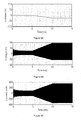
- FIG. 2 shows the stimulus voltage, 3, which has been set to a 125kHz square wave of amplitude 5V. Also shown are the voltages of the FET drain, 4, (also the bottom of the inductor) and the FET source, 5.
- the FET gate voltage (Vgate) is set to 0V.
- the oscillation of the source voltage causes a transition between these two states of FET on and FET off.
- the duty cycle (fraction of the cycle that the FET is on) is controlled by the amplitude of the oscillation. A high level of oscillation gives a near 50% duty cycle, whereas an amplitude less than Vth gives a 0% duty cycle.
- Figure 2B shows the inductor current, which has a more symmetric shape than the voltage.
- the phase difference between the current and the stimulus voltage is approximately 90 degrees and the net power taken from the stimulus voltage by the resonance is low. In fact it is the slight difference from 90 degrees that leads to some net input of energy that maintains the required amplitude for matching to 125kHz.
- the amplitude is not matched to the stimulus frequency (e.g. after a turn on transient, or the stimulus frequency changes, etc) then the relative phase between the stimulus and the current adjusts, resulting in a different power being drained from the stimulus to maintain a new fixed amplitude of resonance.
- This fixed amplitude of resonance sets the duty cycle to match the new stimulus frequency.
- the circuit naturally adjusts to changes in frequency.
- a change in any of the components through temperature or metallic detuning of the inductor would cause a similar response of the circuit, re-tuning to give the correct duty cycle for the stimulus frequency.
- the amplitude of the resonance may be further controlled through the gate voltage Vg.
- Figure 3A shows the profile of Vg, which is initially set to 0V for 5ms to allow turn-on transients to settle. Subsequently it is reduced from 0V to -25V over a 5ms window, and a further 5ms at -25V.
- the effect on the drain voltage and the inductor current is shown in figures 3B and 3C , respectively.
- the lower value of gate voltage means that a larger amplitude is required in order to turn the FET off, since the source needs to be at least Vth below the gate voltage.
- the amplitude of the resonance increases. In this manner, the resonance amplitude may be controlled through the constant gate voltage on the FET.
- Another consequence of the increased amplitude is a changed relative phase between the resonance and the stimulus waveform.
- the current and stimulus waveforms are more in-phase, drawing greater power to maintain the higher resonance amplitude.
- the process of increasing the amplitude through the voltage on the FET gate may continue until the stimulus and resonance are in phase.
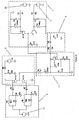
- Figure 4 shows a circuit with the same resonant circuit as figure 1 but with the control portions of Figure 1 shown explicitly as added control circuitry. The functions of the main blocks are indicated on the figure and are now described:
- This block takes as its input the resonance voltage from the FET1 drain and stores the peak negative voltage on C4 (less one diode drop). This stored negative voltage is subsequently used by the gate voltage control block to set the FET1 gate voltage.
- This block has two digital control lines, Vg_ZERO, 10, and Vg_DEC, 11.
- a voltage pulse on Vg_ZERO turns FET2 on and the storage capacitor C5 is connected to ground.
- a voltage pulse on Vg_DEC gives rise to conduction through T1 to the negative voltage rail; the voltage on C5 is made more negative.
- the voltage on C5 may be gradually made more negative or may be zeroed.
- the amplitude of the resonance may either be set with a fixed number of pulses on Vg_DEC or alternatively the gate voltage may be reduced until the amplitude, e.g. measured with an ADC, reaches the desired value.
- An n&p type MOSFET pair are used to control the stimulus voltage applied to the resonance circuit.
- the positive voltage (V1) is coupled in via a shottkey diode with the result that the transient current into the resonance is taken via C10 to ground.
- D6 and V1 supply just the end voltage of the stimulus pulse and enough current to keep the resonance at a constant amplitude.
- This design of stimulus pulse generator is particularly useful if the power supplied to the resonance is required to be monitored. This may be straightforwardly monitored through a measurement of the current pulses through D6. Alternatively if there is no such requirement then C10 and D6 may be removed, provided the 5V supply has sufficient capacitance and low series resistance to efficiently recycle the transient current generated by the resonance.
- the deadband delay generator takes the digital waveform Vstimulus, 12, as its input and generates a deadband delay that avoids shoot-through current in the stimulus FETs.
- the circuit shown in figure 4 enables an inductor current to be set over a range of frequencies determined by the inductor L1 and the capacitors C1, C2, C3, where the amplitude is set by the FET gate voltage. Furthermore the circuit will naturally adjust to different frequencies within this range and also changes in component values (provided the stimulus frequency remains within the range capability of the circuit). As such this approach is tolerant to detuning through temperature, metallic environments, and also manufacturing tolerances on component values.
- the three capacitor network shown in the embodiments is not the exclusive implementation this invention.
- the circuit may be simplified by removing C2 altogether.
- the FET source voltage stays constant when the FET is turned off.
- C2 serves to increase the FET source potential when the FET is off. This acts to turn the FET off further, which minimises leakage through the FET, particularly as the gate potential can vary due to the finite gate voltage storage capacitor C5.
- the task of tuning the reader antenna to a transponder resonance may be carried out with one of the following methods:
- Figure 5 shows an alternative embodiment of the invention.
- this embodiment also includes a p-type FET.
- the state of the n-type FET changes on the negative cycle of the FET drain, and the p-type FET changes on the positive cycle. For low amplitudes both FETs are non-conducting, whereas for high amplitudes both are conducting.
- One feature of this embodiment is that the effect of the FETs and capacitor networks on the waveform is more symmetric than the single FET version. This can lead to an inductor current that has reduced distortion. If this is a requirement to meet emission regulations then it may justify the extra complexity of the circuit.
- the voltage swing of the FET drain, for a given inductor current is reduced relative to the first embodiment. This property may allow the use of FETs with a lower specification of the maximum source-drain voltage. As such the cost of the FETs may be reduced and/or their properties improved through reduced turn-on resistance, etc.
- Figure 6 shows an embodiment of a circuit which can be used to extract power from an rf field, for example for an RFID transponder, or other remotely powered device.
- This circuit is driven by an rf field in which it is located. Power can be taken from the circuit at any convenient point, for example across C1 and rectified.
- To provide a return signal from the transponder power from the circuit may, for example, be used to power an rf oscillator which can be modulated with the return signal.
- the transponder inductance is increased relative to the earlier 300 ⁇ H transmitting antenna example ( figure 1 ). This is to increase the induced voltage in the transponder in response to an oscillating field.
- the Q of the transponder is set by the coil effective series resistance (R1), which has been set to 10 ⁇ in this example, giving a high Q of approximately 80 at 125kHz.
- the n-type MOSFET has a low threshold voltage of 0.5V.
- the transponder circuit is coupled weakly to a transmitting antenna of inductance 300mH.
- the coupling constant between the two inductors is 1%.
- Figure 7A shows the current in the transmitting antenna, which is zero for the first 1ms, then increasing linearly to 50mA by 10ms, then remaining constant amplitude. This waveform has been chosen to illustrate the operation of the circuit.
- Figure 7B shows the corresponding FET drain voltage in the transponder circuit. As the current in the transmitting antenna increases, then so does the current in the transponder circuit antenna and the FET drain voltage increases accordingly. Once the FET drain voltage reaches 0.5V, the threshold voltage of the FET, then the FET begins to conduct over part of each cycle. This allows the resonance to build up in the circuit, matching the duty cycle to the stimulus frequency of 125kHz. There is a marked jump in the FET drain voltage when this matching occurs. At this point the circuit is self-adjusted to the stimulus frequency.
- Figure 8 shows a further development of the transponder circuit.
- an additional branch has been added that couples the FET drain to the gate via diode D1.
- the diode D1 starts to conduct over part of the cycle, pulling the gate voltage low.
- the amplitude of the resonance increases. This process continues until the FET gate voltage reaches the limit set by reverse current flowing in the 5V zener diode (D2).
- the resistor R4 is included to tie the gate voltage to zero in the absence of a resonance in the transponder circuit. As such the transponder circuit is ready for exposure to the reading field.
- the arrangement of Figure 8 automatically controls (lowers) the gate voltage of the FET to increase the amplitude of the resonance to extract increased power from the rf field.
- Figure 9A shows the same transmitter antenna current as figure 7 .
- Figure 9B shows the transponder FET gate voltage, decreasing to negative voltage when the circuit has adjusted to the stimulus frequency (Vdrain exceeds the 0.5V threshold voltage of the FET).
- Figure 9C shows the build up in the transponder circuit resonance as the gate voltage drops.
- the transponder circuit In order for the transponder circuit to adjust to the frequency of the stimulus field and ramp the amplitude of the pickup voltage, it is required that the pickup voltage first exceeds the threshold voltage of the FET. In the above embodiment a low threshold FET has been used such that this may take place at low coupling levels.
- An alternative approach is to increase the inductance of the transponder circuit, which in turn generates a higher voltage in the transponder although with a higher source impedance. In this manner the specific requirement for low threshold may be reduced.
- the resonance may be required to build up to a higher final voltage in order to transfer the same level of power from the energising field. This increased voltage may be required both for powering of the transponder and also for any modulation that the transponder circuit carries out to communicate with the reader.
- a further benefit of the above embodiment occurs when the transponder circuit coupling to the reader is increased.
- one approach is to introduce a regulator to limit the pickup voltage and avoid damage to the rest of the circuitry.
- the transponder may absorb a significant proportion of the energising field, which is subsequently dissipated as heat in the regulator.
- This embodiment however limits the pickup voltage through the relative phase between the transponder resonance and the energising field i.e. the actual level of pickup is reduced, not just withstood through the use of a regulator.
- this embodiment can avoid issues such as the transponder shading the energising field. This may be beneficial when reading multiple transponders.
- this embodiment illustrates how the variable duty cycle technique may be applied to a remotely powered device such as an RFID transponder.
- the circuit may self-adjust to the stimulus field, provided the stimulus frequency is within the range of the transponder circuit and also that the amplitude exceeds the threshold voltage of the FET used together with the capacitor network. It has also been shown that the gate voltage may be automatically ramped such that an increased amplitude of resonance builds in the transponder.
- the transponder circuit described above has several advantages, including as follows:
- the circuit shown in figure 1 is used in free decay, rather than steady state excitation.
- the duty cycle of FET conduction is determined by the decay waveform, and changes as a function of time.
- the resultant behaviour is a chirp signal, rising in frequency as the energy in the circuit decays.
- This embodiment may be used in a reader to detect the presence of a transponder and/or its resonant frequency.
- FIG. 10A shows the decay of the FET drain voltage and figure 10B shows the antenna current.
- the drain voltage is asymmetric when the FET duty cycle is non-zero, which is a natural consequence of the two different capacitances coupled into the resonance.
- the antenna current on the other hand is more symmetric.
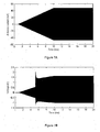
- Figure 10C shows the instantaneous frequency of the chirp as a function of time.
- the chirp starts off at 117.9kHz, rising to a maximum of 144kHz.
- FIG 11A shows the decay envelope of the FET drain voltage. Also overlaid with this trace is a virtually indistinguishable trace of the decay envelope when a resonant transponder has been introduced.
- the transponder comprises a 1mH inductor in parallel with a 1.6nF capacitor, giving a resonant frequency of 125kHz.
- the effective series resistance of the inductor is 50 ⁇ , which gives the transponder a Q of approximately 15.
- the coupling between the reader antenna and the transponder is set low at 0.3%.
- Figure 11B shows the difference in the decay envelopes on the same vertical scale. The result is very low, illustrating their very close match. In fact the maximum difference is approximately 2%, a very low level that would be hard to pick up with a measurement of energy decay.
- figure 12A shows the difference in the actual waveforms between the transponder present and transponder absent.
- This measurement has the great advantage that it is sensitive to differences in phase and the result has much improved sensitivity to the presence of the transponder.
- the transponder absorbs a small proportion of energy, changing the frequency of the decay.
- a phase difference relative to the reference waveform builds up over time and this gives the large difference voltage in figure 12A .
- the voltage difference is maximal at approximately 1.9ms (0.9ms from the start of the chirp), reducing after this time as the chirp decays further.
- the zero duty cycle threshold is approximately 2.15ms.
- Figure 12B shows a similar waveform difference measurement where the transponder frequency has been increased from 125kHz to 134kHz (transponder resonance capacitance decreased from 1.6nF to 1.4nF).
- a change to the difference voltage is clear, in particular the onset of a sharp rise in the difference voltage is delayed with respect to the 125kHz transponder. This is as expected since the chirp frequency is rising with time and therefore matches the new transponder frequency later in the decay.
- the amplitude of the effect is also lower, which is a result of less chirp duration after the transponder has started to have an appreciable effect on the decay.
- the chirp moves into the zero duty cycle region relatively soon after the transponder is excited and the phase difference relative to the reference stops increasing.
- the comparison of figures 12A and 12B shows how the shape of the difference waveform may be used to discriminate between transponders with resonant frequencies 125kHz and 134kHz. Further analysis, particularly of the start point of the difference waveform may allow the transponder frequency to be determined with finer resolution.
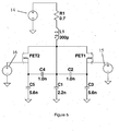
- FIG 13 shows an addition to the fourth embodiment based with an additional capacitor (C4) and FET (FET2) controlled by voltage source 17.
- C4 is much larger than the other resonance capacitors and therefore does not strongly affect the frequency range of the chirp.
- the voltage generated has an amplitude less than 0.7V and does not therefore conduct through the body diode of FET2.
- the voltage at the junction of C1 and C4 may be subsequently taken to an analogue to digital converter (ADC) for sampling.
- ADC an analogue to digital converter
- the ADC will generally have a sample and hold function included such that it digitises the value of the waveform on a timescale significantly less than the time period of that waveform.
- the main advantage of this circuit is that the ADC input may be bypassed by turning FET2 on, in which case the antenna current is returned to ground rather than flowing through C4. In this manner the ADC input, which is set-up for the low power proximity detection of the transponder, is protected when the reader switches into a full power identification mode.
- the large voltages generated in the full power mode, such as at the drain of FET1, are not loaded by the proximity detection circuit elements and therefore do not cause any damage.
- circuit in figure 13 may be used in an alternative manner in which the circuit in figure 13 may be used. If, by the time it is sampled, the chirp is decayed significantly from its start level then a smaller value for the capacitance C4 may be used, still keeping the amplitude below 0.7V (and therefore avoiding the body diode path through FET2). In this manner the voltage sampled by the ADC may be increased (up to 0.7V), improving the signal to noise of the measurement.
- One further alternative is keep FET2 off for the duration of the chirp decay and introduce some gain before the ADC samples the voltage. This may also include a voltage offset such that the dynamic range of the signals is appropriate for the input range of the ADC. An increase in signal to noise by this method is at the expense of power drain from the additional gain circuitry. In order to minimise this additional power drain, the amplification stage may be powered at a reduced duty cycle corresponding to the repeat rate of the chirp.
- the circuits described in the above embodiments provide resonance behaviour, while also responding to a range of frequencies.
- the step up of voltage is achieved through re-cycling transient energy transferred between the inductor and capacitor network.
- a controllable element such as a switching element or transistor, is controlled by a control device including a timing control circuit.
- the methods outlined above allow operation of a high Q LC resonance with a very stable external clock source, such as a crystal resonator. As such a field may be generated efficiently that is very constant with time, both in amplitude/phase and frequency. Such a task is advantageous when implementing a read function of an RFID transponder, as any noise on the reading waveform may translate to noise in the output waveform.
- the 125kHz frequency band chosen for the embodiments is purely by way of example. Applications of the invention are not limited to frequencies around this band, and extend to include all oscillator frequencies ranging from sub-sonic to microwave frequencies and beyond. More specifically to RFID, all common RFID frequency bands are included, such as 125kHz, 134kHz, 13.56MHz, 869MHz, 915MHz, and the like.
Landscapes
- Engineering & Computer Science (AREA)
- Computer Hardware Design (AREA)
- Microelectronics & Electronic Packaging (AREA)
- Near-Field Transmission Systems (AREA)
- Networks Using Active Elements (AREA)
- Oscillators With Electromechanical Resonators (AREA)
- Inductance-Capacitance Distribution Constants And Capacitance-Resistance Oscillators (AREA)
Description
- Broadly, the invention relates to resonant circuits. Embodiments of the invention relate particularly but not exclusively to resonant circuits in RFID (radio frequency identification) responsive to a wide frequency range. Embodiments of the invention also relate to low power proximity detection of an RFID (radio frequency identification) transponder.
- In an RFID system resonant circuits are generally used in both the reader and the transponder. Their use increases the efficiency of energy transfer between the two circuits, which would otherwise be much lower, severely limiting the range of operation. Optimal read range may be achieved when the reader is stimulated at its resonance frequency, and this also matches the resonant frequency of the transponder. The task of operating both these units at their resonant frequencies is complicated by the following factors:
- 1) The LC manufactured components have tolerances on their values, and the resonant frequency will vary between different examples of nominally identical resonant systems.
- 2) Temperature can change the value of the components, making the resonance frequency drift over time and environment.
- 3) Metallic or magnetic objects placed in the vicinity of either antenna can change their inductance and therefore change the resonant frequency.
- 4) The desired resonant frequency can change, for example the regulatory frequency band can change across national boundaries.
- The impact of these complications increases with the Q of the two resonances. As the Q increases then the resonance bandwidth drops proportionally and a closer match between the two frequencies is required for efficient power transfer. Such constraints may limit the Q of the two circuits to relatively low levels, which may in turn limit the read range and/or lead to excessive power requirements.
- In RFID systems one approach to mitigate some of these complications is to use a tuning circuit. A large number of different tuning variants have been disclosed in the prior art, however they have some common features. In order to tune the resonance frequency then either an electrically tuneable component, such as a varactor or electrically variable inductor, or more commonly a combination of discrete capacitors or inductors are coupled into the resonance. An exemplary reference is
US6317027 , where a set of tuning capacitors in binary weighting are selectively coupled into the reader resonance with corresponding variations in the resonance frequency. - The adjustment may be carried out in a tuning cycle separate from the normal read and/or write operations.
US6317027 is an example of such an approach, where a sweep of the tuning capacitance is carried out and the resonance amplitude profile determined; the chosen tuning capacitance achieves the maximum amplitude in the reader antenna. AlternativelyUS5491715 discloses a method based on the phase difference between the stimulus and the resonance to determine how far from resonance the reader circuit is. - These prior art methods to tune a system to resonance at a desired frequency have some significant drawbacks, which are now outlined.
- The tuning circuit can require many components, comprising the set of capacitors and the switches to couple them into the resonance; this adds to the system complexity and cost. If fine control over the frequency is required then the selectable capacitors are required at high accuracy in order to achieve a monotonic setting of the total tuning capacitance. Such constraints can limit the feasible tuning accuracy and resolution.
- The tuning is not generally real-time. If it is made real-time, such as the method described in
US5491715 , then this adds complexity and cost. Real-time control is beneficial to cope with transient de-tuning effects such as temperature drift and metallic objects coming into range. - These prior art tuning methods are generally applied to the reader antenna only. A transponder is required to have its natural resonance close to the radio frequency energising field in order to obtain its power. If significantly de-tuned, then the transponder would not be able to charge up enough to run a tuning circuit. As such, the prior art tuning methods described are usually unsuitable for a passive transponder.
- Because of tight cost and power constraints it is more common that transponders are set up at manufacture with a fixed tuning. The fixed tuning being set according to their target operating. This fixed tuning step adds to the cost of manufacture and cannot adjust to environmental changes that might affect the transponder resonant frequency.
- A further transponder consideration is that it may be advantageous for a single transponder to be able to respond to a range of frequencies. One application example is the use of the same transponder across borders with different regulatory operating bands. If the transponders may respond to the different frequencies permitted in each region without a re-tuning step then this facilitates international travel, a key requirement in the common RFID application of asset tracking. Prior art methods provide no facility for this.
- Further prior art may be found in
US2774060 ,US3818472 ,US6476708 , andGB2278631 WO2005/104022 ,US2004/0214549 ,GB2321726 US3842246 ,GB2087564 GB1206925 US2003/006880 describes a device and method for contactless transmission of power or data. - According to an aspect of the present invention there is provided a controllable electric resonator as recited in
claim 1. According to a further aspect of the present invention there is provided a method of controlling a resonant frequency of a resonant circuit as recited inclaim 10. - Further embodiments of the present invention are recited in the dependent claims.
- We will describe an LC circuit that is responsive to a range of stimulus frequencies without the requirement for control of a tuning circuit. In embodiments the circuit is able to adjust naturally to external environmental influences without additional control mechanisms. In embodiments the circuit requires only a small number of low tolerance electrical components.
- Rather than using a range of capacitors that are fully coupled into the resonance i.e. 100% duty cycle, in embodiments an alternative approach is taken where the LC resonance comprises a primary capacitive path and one or more secondary capacitive paths that are coupled into the resonance with a variable duty cycle. Depending on the duty cycle, the resonance matches a different stimulus frequency.
- In embodiments the duty cycle is set by a switching element, more particularly a FET with a source potential that varies with the resonance amplitude. The charge required to turn the FET on or off is supplied by the resonance current in the inductor; it is therefore efficient and does not require an external power source; as such the method may have application both in a reader and also a transponder. If implemented in a transponder then the transponder will be responsive to a range of energising frequencies, potentially allowing operation across locations with different regulatory frequencies.
- The duty cycle is determined both by the resonance amplitude and also the FET gate voltage. The resonance amplitude may be conveniently controlled with the FET gate voltage, which through the relative phase of the resonance and stimulus sets the steady state amplitude. The amplitude may be straightforwardly controlled up to a maximum level corresponding to that of an antenna circuit matched to the stimulus frequency with the same Q. At this maximum level the resonance is in phase with the stimulus.
- In high coupling situations a transponder may include a regulator to limit the pickup voltage and avoid damage to the rest of the circuitry. However such a transponder can pickup a significant proportion of the energising field, which is subsequently dissipated as heat in the regulator. Embodiments of the transponder we describe limit the pickup voltage through the relative phase between the pickup voltage and the energising field. The level of pickup is limited in the high coupling case, which can avoid issues with the transponder shading the energising field. This can be beneficial when reading multiple transponders.
- In embodiments the reader and/or the transponder may be tolerant to a degree of detuning due to the environment. For example a metallic element placed close to the antenna will modify its inductance. However, provided the desired operating frequency is still encompassed in the frequency range over which the resonance is responsive then the system will continue to operate normally. This offers an improvement relative to the prior art where such environmental changes are generally only corrected in the reader and require a separate control/measurement process.
- In a first aspect of the invention there is therefore provided a controllable electric resonator comprising an inductor coupled to a first capacitor to form a resonant circuit, the resonator further comprising a controllable element, a second capacitor controllably coupled across said first capacitor by said controllable element, and a control device to control said controllable element such that a total effective capacitance of said first and second capacitor varies over a duty cycle of an oscillatory signal on said resonator.
- In some preferred embodiments the controllable device comprises a switching element such as a transistor, more particularly a field effect transistor such as a MOS (metal oxide semiconductor) transistor, and a control device comprises a bias circuit for the transistor. Preferably the bias circuit is configured to automatically adjust the bias from the transistor to increase an amplitude of the oscillatory signal. Optionally the resonator may include a power supply circuit to derive a power supply for said bias circuit from said oscillatory signal.
- In embodiments the resonator includes a third capacitor connected across the controllable element; preferably the inductor has a Q of greater than 50, more preferably greater than 100. The resonator preferably includes a drive system to drive the oscillatory signal on the resonator; this may include means for converting a current drawn by the resonator into a pulse having a duration depending on the current.
- The invention further provides an RFID tag or tag reader including a resonator as described above.
- In a related aspect the invention provides a method of controlling the amplitude of oscillations in a resonant circuit driven by an oscillatory signal, the method comprising: applying a reactive element to said resonant circuit with a variable coupling; varying said coupling over a cycle of said oscillatory signal to control said amplitude of oscillations.
- The invention further provides apparatus for controlling the amplitude of oscillations on a resonant circuit driven by an oscillatory signal, the apparatus comprising: means for applying a reactive element to said resonant circuit with a variable coupling; and means for varying said coupling over a cycle of said oscillatory signal to control said amplitude of oscillations.
- The invention still further provides a method of controlling a resonant frequency of a resonant circuit to substantially match said resonant frequency to a frequency of an external waveform, the resonant circuit comprising an inductance coupled to a capacitance, the capacitance having a switched component of capacitance, the method comprising controlling a duty cycle of said switched component of capacitance, in response to a signal level of a waveform of an oscillation of said resonant circuit.
- The inductance may be coupled in series and/or in parallel with the capacitance; preferably the switched component of capacitance includes a field effect transistor (FET) switch coupled (in series and/or parallel) to a switched capacitance. The duty cycle may be controlled by controlling a gate-source voltage of the FET in response to an instantaneous level of the waveform of an oscillation of the resonant circuit. In embodiments a relative phase of the waveform of this oscillation and of the external waveform changes in response to a signal level of the external waveform.
- Thus, in embodiments, broadly speaking the amplitude of the waveform in the resonant circuit builds up and controls the gate-source voltage of the FET to bring the circuit towards resonance. When resonant oscillation has been established, broadly speaking the amplitude of the oscillatory waveform in a resonant circuit remains approximately constant but the relative phase of the "internal" waveform in the resonant circuit with respect to the external waveform changes in response to the strength of the external signal; and as previously mentioned the duty cycle depends upon the frequency of the external signal. Broadly speaking the relative phase measures the amount of energy extracted from the stimulating field. One advantage of this operation is that the circuit can operate over a very wide range of external field strengths and, for example, does not need an additional regulator when operating in close proximity to an rf source, that is in a high field.
- In some embodiments of the method the external waveform comprises a waveform of an rf electromagnetic field (either propagating or near-field). Thus an embodiment of the above-described method is advantageous for extracting energy from an rf electromagnetic field, in embodiments the aforementioned relative phase adjusting to limit the extracted energy from the field as the field increases. (In embodiments the amplitude of the internal waveform is a function of the gate voltage of the FET, of component values, and of the resonant frequency).
- In other embodiments of the method the external waveform may be derived from a crystal oscillator, either directly or indirectly (for example via microprocessor). Since in embodiments the circuit adjusts to the clock such a technique can be employed to provide a very low phase noise rf source.
- In a related aspect the invention provides a circuit for controlling a resonant frequency of a resonant circuit to substantially match said resonant frequency to a frequency of an external waveform, the resonant circuit comprising an inductance coupled to a capacitance, the capacitance having a switched component of capacitance, the circuit comprising means for controlling a duty cycle of said switched component of capacitance in response to a signal level of a waveform of an oscillation of said resonant circuit.
- Broadly speaking embodiments of the circuit are useful where very efficient coupling over a relatively wide range of frequencies is desirable. Embodiments of the circuit facilitate coupling between two high Q systems without the need for very precise alignment of the resonant peaks which would otherwise be necessary. This facilitates, for example, highly efficient inductive charging. Embodiments of the technique also facilitate the efficient operation of an rf tag over a plurality of frequencies or bands of operation, for example facilitating the provision of a single tag capable of operating in accordance with different US and European prescribed frequency standards (for example over the range 125 KHz to 134 KHz).
- Thus the invention further provides an RFID tag comprising a controllable resonant circuit, the resonant circuit comprising an inductance coupled to a capacitance, the capacitance having a switched component of capacitance, wherein said controllable resonant circuit is configured to automatically control a duty cycle of said switched component of capacitance to select one of a plurality of frequencies of operation of said tag in response to an interrogating rf field.
- The invention also provides an LC resonant circuit comprising an inductor, a primary capacitive path, and at least one other secondary capacitive path that is coupled into the resonance with a variable duty cycle; and wherein the circuit response frequency, which is dependent on the duty cycle, matches to a stimulus frequency.
- The invention further provides a reader antenna tuning method in which the stimulus frequency is varied and the chosen frequency maximises the energy input into the antenna. The invention further provides a reader antenna tuning method where the stimulus frequency is varied and the chosen frequency minimises the threshold amplitude for transponder modulation. The invention further provides a reader antenna tuning method where the stimulus frequency is varied and the chosen frequency makes the modulation transformed transponder impedance resistive. In a reader as previously described the tuning frequency to match to the transponder may be taken from a low power proximity detector using a chirp decay to measure one or both of the transponder proximity and its resonant frequency. In embodiments the transponder is responsive to a range of frequencies.
- A controllable electric resonator, resonant circuit, apparatus, tag or reader, or method as described above may be incorporated into one or more of the following: a transmitter; a receiver; a near-field communication device; an inductive charger; an inductively charged device such as a consumer electronics device; an oscillator; a voltage converter; a capacitive energy/information transfer system; and an energy harvesting device.
- We also describe a low power detection method for the presence of a RFID transponder. The system may move into a full power identification mode when the presence of a transponder is detected.
- Rather than a conventional LC reader antenna resonant circuit, these embodiments use a circuit that contains a non-linear element, such that the natural resonance frequency depends on amplitude. In response to a pulse excitation the reader antenna circuit generates a chirp signal that simultaneously decays with time and sweeps across a frequency range.
- The antenna circuit has a preferably significantly higher Q than the transponder such the decay of the chirp is relatively slow compared to the transponder response. In this manner there is still an appreciable duration of the antenna waveform when the transponder frequency is close to the chirp instantaneous frequency. When this occurs the transponder absorbs energy from the antenna, which is subsequently registered in the reader. This chirp method therefore no longer requires matching between the resonant frequency of the antenna and the transponder.
- Embodiments employ a decaying chirp waveform that links the amplitude of the chirp to the frequency of the chirp. This waveform allows a more sensitive measurement of energy loss through the phase of the decaying waveform. Small changes in the energy absorbed from the antenna cause corresponding changes to the frequency of the decay, in addition to the amplitude. Comparing two levels of damping, once the, two chirps are operating at different frequencies their phase difference increases with time. Consequently, after a delay of many cycles the small difference in damping between the two waveforms may be picked up by a straightforward sampling of the chirp waveform. The phase difference between the two waveforms, once it amounts to a significant fraction of a cycle, translates to a large fractional change in the sampled voltage. This is in contrast to an amplitude measurement, which would display a much smaller effect. Registering changes in damping through the phase of the chirp decay can potentially offer improved sensitivity.
- The frequency sweep of the chirp decay may be used to determine the transponder resonant frequency. As the frequency sweeps over the transponder resonance, the effect of the transponder on the antenna is maximised. For the case where the chirp starts at low frequency and sweeps to a higher frequency then the effect of increasing the transponder resonant frequency is to delay the corresponding change to the chirp. Rather than sampling the chirp at one point only, sampling at a number of points along the length of the decay therefore provides information relating to the transponder resonance frequency. This measurement may either be carried out every time the chirp is generated, or alternatively a change in the system may be registered from a single point measurement and subsequently the transponder frequency determined from a multi-point measurement of the chirp. Once the transponder resonant frequency has been determined the antenna may be tuned accordingly for the subsequent full power identification mode. This multi-point measurement may also beneficially discriminate between a transponder with a clear resonance and interfering objects that absorb energy over a wide frequency range, for example metallic objects.
- Thus there is also provided a resonant circuit with a non-linear element in it such that on pulsing it produces a chirp decay that links the amplitude to the decay. A measurement of phase is used to determine small differences due to the presence of an object. Preferably the circuit uses at least one FET and variable duty cycle of two capacitive branches in order to generate the chirp. Preferably the circuit uses a varactor or an electrically variable inductor as the nonlinear element that generates the chirp. The object to detect may be an RFID transponder, a passive resonant circuit, a metallic object; the object may be coupled inductively or capacitively. Averaging sequential samples may be used to track environmental changes or battery droop and/or to reduce noise interference. We also describe a cat flap or pet feeder with a built in RFID reader, where a low power mode is used to detect the presence of a cat prior to full power reading of a sub-dermal RFID chip.
-
-
Figure 1 is a schematic of a first embodiment of a resonant circuit. -
Figure 2A is a plot of the voltage waveforms of the first embodiment of the resonant circuit with zero volts on the FET gate.Figure 2B is the corresponding plot of the antenna current. -
Figure 3A is a plot of the FET gate voltage reducing to negative potential when the circuit is resonating.Figures 3B and 3C are the corresponding voltage and antenna current waveforms, respectively. -
Figure 4 is a schematic of an embodiment of a tag reader comprising a resonant circuit as shown inFigure 1 with added sections to control the FET gate voltage and supply the stimulus signals. -
Figure 5 is a schematic of a second embodiment of a resonant circuit. -
Figure 6 is a schematic of an embodiment of a transponder comprising a resonant circuit. -
Figure 7A and 7B are plots of the antenna current and voltage respectively for the transponder offigure 6 , excited by an external field. -
Figure 8 is a schematic of an embodiment of a transponder comprising a resonant circuit as shown inFigure 6 with added circuit elements to build up the amplitude of the resonance through the FET gate voltage. -
Figure 9A is a plot of the antenna current for the transponder offigure 8 , excited by an external field.Figures 9B and 9C are the corresponding plots of the FET gate voltage and antenna voltage, respectively. -
Figures 10A and 10B are decay waveforms of a fourth embodiment of a resonant circuit, where the circuit offigure 1 is excited with a 4us pulse.Figure 10C is the instantaneous frequency of the free decay.. -
Figure 11A is a graph showing an envelope function of the voltage decay infigure 10A , overlaid with a similar trace where a 125kHz transponder is present in the proximity of the reader.Figure 11B is the difference between these two envelope functions plotted on the same vertical scale. -
Figure 12A is the difference between the two decay waveforms with and without the transponder present.Figure 12B is a similar difference waveform where the transponder resonance frequency has been increased from 125kHz to 134kHz. -
Figure 13 is a schematic a resonant circuit with added components to sample the amplitude of a chirp decay for proximity detection. - (In
Figures 3 ,7 ,9 ,10 and12 , although printing artefacts may appear, the areas within the signal envelopes should be solid because of the time scale on which the waveforms are depicted). - The following description of a resonant circuit responsive to a wide frequency range is merely exemplary in nature and is in no way intended to limit the invention or its applications or uses. Those skilled in the art will recognise that in addition to the field of RFID it may equally well be applied in alternative fields benefiting from the properties of such a resonant circuit. These include (but are not limited to) the following:
- 1) radio transmitters and receivers, including mobile telephone
- 2) near field communications
- 3) inductive charging of device
- 4) oscillators
- 5) voltage converters
- 6) capacitive energy/information transfer between systems
- 7) energy harvesting e.g. wirelessly from an electromagnetic source or within a circuit such as a mechanical pickup.
-
Figure 1 shows a first embodiment of a resonant circuit according to an aspect of the invention. A high Q antenna comprises 32 turns of 660-strand 46AWG Litz wire, with overall diameter approximately 20cm. Around the target operating frequency of 125kHz the antenna has inductance 300µH (L1) and effective series resistance 0.7Ω (R1), giving a Q of 340. The antenna is placed in series with the capacitor network C1, C2, C3 and an n-type FET. The FET gate voltage is controlled by the voltage source Vgate, 1, and the system is excited by the voltage source Vstimulus, 2. The operating principle is now described with reference to the current and voltage waveforms plotted infigure 2 . -
Figure 2 shows the stimulus voltage, 3, which has been set to a 125kHz square wave ofamplitude 5V. Also shown are the voltages of the FET drain, 4, (also the bottom of the inductor) and the FET source, 5. The FET gate voltage (Vgate) is set to 0V. There are two clear states of the circuit as follows: - 1) The FET is turned on when the source voltage is below the gate voltage (0V) by at least the 2V threshold voltage (Vth) of the FET. In this state the source-drain capacitor C2 is shorted and the source and drain voltages are very close to each other.
- 2) The FET is turned off when the source voltage is greater than -Vth, in which case the source and drain voltages diverge and the source-drain capacitor charges up.
- With the gate voltage fixed (at 0V), the oscillation of the source voltage causes a transition between these two states of FET on and FET off. The duty cycle (fraction of the cycle that the FET is on) is controlled by the amplitude of the oscillation. A high level of oscillation gives a near 50% duty cycle, whereas an amplitude less than Vth gives a 0% duty cycle. These two extremes of duty cycle correspond to two extremes of frequency, given by the following equations:


- For the capacitance values of this example these two frequencies are f50% = 106kHz, f0% = 145kHz. Therefore, depending on the amplitude of oscillation, this circuit is able to respond at any frequency within this range. The frequency chosen in this example leads to an amplitude of oscillation that peaks at approximately +26V, which together with the 2V Vth of the FET gives the appropriate duty cycle for 125kHz. The asymmetry of the waveforms is a natural consequence of the change in effective capacitance in series with the inductor.
-
Figure 2B shows the inductor current, which has a more symmetric shape than the voltage. The phase difference between the current and the stimulus voltage is approximately 90 degrees and the net power taken from the stimulus voltage by the resonance is low. In fact it is the slight difference from 90 degrees that leads to some net input of energy that maintains the required amplitude for matching to 125kHz. When the amplitude is not matched to the stimulus frequency (e.g. after a turn on transient, or the stimulus frequency changes, etc) then the relative phase between the stimulus and the current adjusts, resulting in a different power being drained from the stimulus to maintain a new fixed amplitude of resonance. This fixed amplitude of resonance sets the duty cycle to match the new stimulus frequency. As such the circuit naturally adjusts to changes in frequency. At this point it is worth noting that a change in any of the components through temperature or metallic detuning of the inductor would cause a similar response of the circuit, re-tuning to give the correct duty cycle for the stimulus frequency. - The amplitude of the resonance may be further controlled through the gate voltage Vg.
Figure 3A shows the profile of Vg, which is initially set to 0V for 5ms to allow turn-on transients to settle. Subsequently it is reduced from 0V to -25V over a 5ms window, and a further 5ms at -25V. The effect on the drain voltage and the inductor current is shown infigures 3B and 3C , respectively. The lower value of gate voltage means that a larger amplitude is required in order to turn the FET off, since the source needs to be at least Vth below the gate voltage. In order to set the same duty cycle to match 125kHz the amplitude of the resonance increases. In this manner, the resonance amplitude may be controlled through the constant gate voltage on the FET. - Another consequence of the increased amplitude is a changed relative phase between the resonance and the stimulus waveform. The current and stimulus waveforms are more in-phase, drawing greater power to maintain the higher resonance amplitude. The process of increasing the amplitude through the voltage on the FET gate may continue until the stimulus and resonance are in phase.
-
Figure 4 shows a circuit with the same resonant circuit asfigure 1 but with the control portions ofFigure 1 shown explicitly as added control circuitry. The functions of the main blocks are indicated on the figure and are now described: - This is as described for
figure 1 . - This block takes as its input the resonance voltage from the FET1 drain and stores the peak negative voltage on C4 (less one diode drop). This stored negative voltage is subsequently used by the gate voltage control block to set the FET1 gate voltage.
- This block has two digital control lines, Vg_ZERO, 10, and Vg_DEC, 11. A voltage pulse on Vg_ZERO turns FET2 on and the storage capacitor C5 is connected to ground. A voltage pulse on Vg_DEC gives rise to conduction through T1 to the negative voltage rail; the voltage on C5 is made more negative. Using the digital control lines the voltage on C5 may be gradually made more negative or may be zeroed. This is connected to FET1 gate and so controls the amplitude of the oscillation of the resonance circuit. The amplitude of the resonance may either be set with a fixed number of pulses on Vg_DEC or alternatively the gate voltage may be reduced until the amplitude, e.g. measured with an ADC, reaches the desired value.
- An n&p type MOSFET pair are used to control the stimulus voltage applied to the resonance circuit. The positive voltage (V1) is coupled in via a shottkey diode with the result that the transient current into the resonance is taken via C10 to ground. D6 and V1 supply just the end voltage of the stimulus pulse and enough current to keep the resonance at a constant amplitude. This design of stimulus pulse generator is particularly useful if the power supplied to the resonance is required to be monitored. This may be straightforwardly monitored through a measurement of the current pulses through D6. Alternatively if there is no such requirement then C10 and D6 may be removed, provided the 5V supply has sufficient capacitance and low series resistance to efficiently recycle the transient current generated by the resonance.
- Lastly, the deadband delay generator takes the digital waveform Vstimulus, 12, as its input and generates a deadband delay that avoids shoot-through current in the stimulus FETs.
- In summary the circuit shown in
figure 4 enables an inductor current to be set over a range of frequencies determined by the inductor L1 and the capacitors C1, C2, C3, where the amplitude is set by the FET gate voltage. Furthermore the circuit will naturally adjust to different frequencies within this range and also changes in component values (provided the stimulus frequency remains within the range capability of the circuit). As such this approach is tolerant to detuning through temperature, metallic environments, and also manufacturing tolerances on component values. - The description above has been in terms of a square wave stimulus waveform. However, this also may be a reduced duty cycle waveform, provided it can supply sufficient energy to maintain the resonance. An alternative approach is to stimulate the circuit with a waveform at a sub-harmonic of the target frequency. The main advantage of this scheme is that the n&p stimulus FETs are switched less often, leading to reduced losses in the charging/discharging of these components. A more efficient circuit operation may therefore be achieved.
- The three capacitor network shown in the embodiments is not the exclusive implementation this invention. In fact the circuit may be simplified by removing C2 altogether. In this case the FET source voltage stays constant when the FET is turned off. However it has generally been found advantageous to include some capacitance for C2, which serves to increase the FET source potential when the FET is off. This acts to turn the FET off further, which minimises leakage through the FET, particularly as the gate potential can vary due to the finite gate voltage storage capacitor C5.
- The task of tuning the reader antenna to a transponder resonance may be carried out with one of the following methods:
- 1) The reader may step or sweep the stimulus frequency and monitor the power drain from the transponder. This may be carried out by monitoring the power drain from the 5V source.
- 2) The reader may step or sweep the stimulus amplitude and frequency with the aim to determine the threshold amplitude as a function of frequency where the transponder modulation may be picked up. The lowest threshold amplitude will generally be at the transponder resonance frequency.
- 3) When the transponder modulates with a normal resistive load modulation then the transformed transponder impedance seen by the reader is also a resistive modulation when operating at the transponder resonance. When the operating frequency is different to the transponder resonance a reactive component is present in the transformed impedance. The reader may monitor the transformed-impedance and adjust the frequency until a resistive impedance results.
- 4) The circuit may be periodically stimulated with a pulse, generating a decaying resonant waveform. The amplitude of oscillation is linked to the natural frequency of the oscillation through the duty cycle of the capacitive paths. The result is that the free decay also sweeps over a frequency range i.e. it generates a decaying chirp. Such a signal may be used to sweep over the potential transponder frequencies. Waveform differences with respect to a reference trace may be used to indicate the frequency of maximum absorption from the reader. This frequency would correspond to the transponder resonant frequency and the reader may be tuned accordingly. Such a system may be used as a low power method to detect the presence of a transponder and also its resonant frequency. Once detected the reader may read the transponder in the normal way. This method is implemented in the 4th embodiment of the invention.
-
Figure 5 shows an alternative embodiment of the invention. In addition to the n-type FET shown infigure 1 , this embodiment also includes a p-type FET. The state of the n-type FET changes on the negative cycle of the FET drain, and the p-type FET changes on the positive cycle. For low amplitudes both FETs are non-conducting, whereas for high amplitudes both are conducting. The design equations for the frequency limits at 0% duty cycle and 100% duty cycle (duty cycle is the fraction of the cycle that at least one of the FETs is conducting) are as follows:

- The values shown in
figure 5 give a frequency range of f100%= 104kHz and f100%=147kHz. When setting the amplitude of the resonance with the gate voltages Vgate1, 15, and Vgate2, 16, this is done in a similar manner to the single FET version of the first embodiment except that these voltages should go in opposite directions. Vgate1 is reduced to negative voltages and Vgate2 is increased to positive voltages by the same amount. - One feature of this embodiment is that the effect of the FETs and capacitor networks on the waveform is more symmetric than the single FET version. This can lead to an inductor current that has reduced distortion. If this is a requirement to meet emission regulations then it may justify the extra complexity of the circuit. In addition, the voltage swing of the FET drain, for a given inductor current, is reduced relative to the first embodiment. This property may allow the use of FETs with a lower specification of the maximum source-drain voltage. As such the cost of the FETs may be reduced and/or their properties improved through reduced turn-on resistance, etc.
-
Figure 6 shows an embodiment of a circuit which can be used to extract power from an rf field, for example for an RFID transponder, or other remotely powered device. This circuit is driven by an rf field in which it is located. Power can be taken from the circuit at any convenient point, for example across C1 and rectified. To provide a return signal from the transponder power from the circuit may, for example, be used to power an rf oscillator which can be modulated with the return signal. The transponder inductance is increased relative to the earlier 300µH transmitting antenna example (figure 1 ). This is to increase the induced voltage in the transponder in response to an oscillating field. The capacitors C1, C2, C3 are reduced by the same factor resulting in the same frequency range as the first embodiment (f50% = 106kHz, f10% = 145kHz). The Q of the transponder is set by the coil effective series resistance (R1), which has been set to 10Ω in this example, giving a high Q of approximately 80 at 125kHz. The n-type MOSFET has a low threshold voltage of 0.5V. - The transponder circuit is coupled weakly to a transmitting antenna of inductance 300mH. The coupling constant between the two inductors is 1%.
Figure 7A shows the current in the transmitting antenna, which is zero for the first 1ms, then increasing linearly to 50mA by 10ms, then remaining constant amplitude. This waveform has been chosen to illustrate the operation of the circuit. -
Figure 7B shows the corresponding FET drain voltage in the transponder circuit. As the current in the transmitting antenna increases, then so does the current in the transponder circuit antenna and the FET drain voltage increases accordingly. Once the FET drain voltage reaches 0.5V, the threshold voltage of the FET, then the FET begins to conduct over part of each cycle. This allows the resonance to build up in the circuit, matching the duty cycle to the stimulus frequency of 125kHz. There is a marked jump in the FET drain voltage when this matching occurs. At this point the circuit is self-adjusted to the stimulus frequency. -
Figure 8 shows a further development of the transponder circuit. Here an additional branch has been added that couples the FET drain to the gate via diode D1. Once the circuit adjusts to the stimulus frequency and the amplitude of the voltage on the FET drain jumps above 0.5V, the diode D1 starts to conduct over part of the cycle, pulling the gate voltage low. As the gate voltage drops to negative voltage, the amplitude of the resonance increases. This process continues until the FET gate voltage reaches the limit set by reverse current flowing in the 5V zener diode (D2). The resistor R4 is included to tie the gate voltage to zero in the absence of a resonance in the transponder circuit. As such the transponder circuit is ready for exposure to the reading field. Broadly the arrangement ofFigure 8 automatically controls (lowers) the gate voltage of the FET to increase the amplitude of the resonance to extract increased power from the rf field. - The operation of the circuit described above is illustrated by the waveforms in
figure 9. Figure 9A shows the same transmitter antenna current asfigure 7 .Figure 9B shows the transponder FET gate voltage, decreasing to negative voltage when the circuit has adjusted to the stimulus frequency (Vdrain exceeds the 0.5V threshold voltage of the FET).Figure 9C shows the build up in the transponder circuit resonance as the gate voltage drops. - In order for the transponder circuit to adjust to the frequency of the stimulus field and ramp the amplitude of the pickup voltage, it is required that the pickup voltage first exceeds the threshold voltage of the FET. In the above embodiment a low threshold FET has been used such that this may take place at low coupling levels. An alternative approach is to increase the inductance of the transponder circuit, which in turn generates a higher voltage in the transponder although with a higher source impedance. In this manner the specific requirement for low threshold may be reduced. However with a high transponder circuit inductance, the resonance may be required to build up to a higher final voltage in order to transfer the same level of power from the energising field. This increased voltage may be required both for powering of the transponder and also for any modulation that the transponder circuit carries out to communicate with the reader.
- A further benefit of the above embodiment occurs when the transponder circuit coupling to the reader is increased. At high coupling levels one approach is to introduce a regulator to limit the pickup voltage and avoid damage to the rest of the circuitry. One drawback of this approach is that the transponder may absorb a significant proportion of the energising field, which is subsequently dissipated as heat in the regulator. This embodiment however limits the pickup voltage through the relative phase between the transponder resonance and the energising field i.e. the actual level of pickup is reduced, not just withstood through the use of a regulator. Through this improved behaviour in the high coupling case, this embodiment can avoid issues such as the transponder shading the energising field. This may be beneficial when reading multiple transponders.
- In summary, this embodiment illustrates how the variable duty cycle technique may be applied to a remotely powered device such as an RFID transponder. The circuit may self-adjust to the stimulus field, provided the stimulus frequency is within the range of the transponder circuit and also that the amplitude exceeds the threshold voltage of the FET used together with the capacitor network. It has also been shown that the gate voltage may be automatically ramped such that an increased amplitude of resonance builds in the transponder.
- The transponder circuit described above has several advantages, including as follows:
- 1. A high Q transponder may be used without the usual complications of precise matching of the stimulus field to the transponder frequency; the transponder adjusts to the stimulus frequency.
- 2. The system is more tolerant to variations in temperature and metallic environment that can affect the transponder frequency. Provided the stimulus is within the frequency range of the transponder circuit, a degree of variation in the component values will not affect the operation.
- 3. The system is more tolerant to variations in component values at manufacture. As such careful tuning of the component values may not be required, leading to a potentially lower cost of manufacture. This can also facilitate manufacturing techniques that may not currently be able to achieve the tolerances required for prior art implementations. Examples of such techniques may include printed electronics and organic semiconductors.
- 4. The transponder can respond to more than one reader frequency. As such, transport across international borders where the regulatory frequency band changes may be tolerated.
- 5. The action of the circuit with a fixed gate is similar to a regulator. The gate voltage sets the amplitude at which the duty cycle matches the stimulus frequency. The main change that an increase in coupling constant has is to change the relative phase of the stimulus and transponder response. The amplitude of the transponder resonance stays approximately the same. As such, an additional regulator may not be necessary in the transponder. This also reduces the effect of a closely coupled transponder shading the reader field from additional transponders.
- In a fourth embodiment, the circuit shown in
figure 1 is used in free decay, rather than steady state excitation. When used in free decay, the duty cycle of FET conduction is determined by the decay waveform, and changes as a function of time. The resultant behaviour is a chirp signal, rising in frequency as the energy in the circuit decays. This embodiment may be used in a reader to detect the presence of a transponder and/or its resonant frequency. - A 4µs square voltage pulse of
amplitude 5V is applied to Vstimulus, 2, and the FET gate voltage, 1, is kept at 0V.Figure 10A shows the decay of the FET drain voltage andfigure 10B shows the antenna current. The drain voltage is asymmetric when the FET duty cycle is non-zero, which is a natural consequence of the two different capacitances coupled into the resonance. The antenna current on the other hand is more symmetric. -
Figure 10C shows the instantaneous frequency of the chirp as a function of time. The chirp starts off at 117.9kHz, rising to a maximum of 144kHz. The high frequency limit compares well to a predicted f0% of 145kHz, however the start frequency is above the other limit of f50% = 106kHz. This is because 50% duty cycle is only approached where the amplitude is much greater than the threshold voltage Vth. If a lower starting frequency is required for the same capacitive network then one or more of the following methods may be employed: - 1) Increase the initial amplitude of the oscillation, for example by a double pulse stimulus.
- 2) Change the FET for one with a lower Vth.
- 3) Put a positive gate voltage on the FET of amplitude less than Vth. This keeps the operation of the circuit the same i.e. the FET conducts only on the negative cycle of the FET source voltage. However, the amplitude required for FET turn on with such a positive gate voltage is reduced.
-
Figure 11A shows the decay envelope of the FET drain voltage. Also overlaid with this trace is a virtually indistinguishable trace of the decay envelope when a resonant transponder has been introduced. The transponder comprises a 1mH inductor in parallel with a 1.6nF capacitor, giving a resonant frequency of 125kHz. The effective series resistance of the inductor is 50Ω, which gives the transponder a Q of approximately 15. The coupling between the reader antenna and the transponder is set low at 0.3%. -
Figure 11B shows the difference in the decay envelopes on the same vertical scale. The result is very low, illustrating their very close match. In fact the maximum difference is approximately 2%, a very low level that would be hard to pick up with a measurement of energy decay. - Rather than looking at the decay envelope,
figure 12A shows the difference in the actual waveforms between the transponder present and transponder absent. This measurement has the great advantage that it is sensitive to differences in phase and the result has much improved sensitivity to the presence of the transponder. As the chirp decays and sweeps through its frequency range, the transponder absorbs a small proportion of energy, changing the frequency of the decay. A phase difference relative to the reference waveform builds up over time and this gives the large difference voltage infigure 12A . The voltage difference is maximal at approximately 1.9ms (0.9ms from the start of the chirp), reducing after this time as the chirp decays further. Note that once the amplitude of the chirp decays below Vth and the duty cycle of the FET is zero, the phase difference between the traces stays constant and the difference waveform decays with amplitude of the chirp; in this example the zero duty cycle threshold is approximately 2.15ms. -
Figure 12B shows a similar waveform difference measurement where the transponder frequency has been increased from 125kHz to 134kHz (transponder resonance capacitance decreased from 1.6nF to 1.4nF). A change to the difference voltage is clear, in particular the onset of a sharp rise in the difference voltage is delayed with respect to the 125kHz transponder. This is as expected since the chirp frequency is rising with time and therefore matches the new transponder frequency later in the decay. The amplitude of the effect is also lower, which is a result of less chirp duration after the transponder has started to have an appreciable effect on the decay. The chirp moves into the zero duty cycle region relatively soon after the transponder is excited and the phase difference relative to the reference stops increasing. The comparison offigures 12A and 12B shows how the shape of the difference waveform may be used to discriminate between transponders with resonant frequencies 125kHz and 134kHz. Further analysis, particularly of the start point of the difference waveform may allow the transponder frequency to be determined with finer resolution. -
Figure 13 shows an addition to the fourth embodiment based with an additional capacitor (C4) and FET (FET2) controlled byvoltage source 17. When the FET is turned off the antenna current flows through C4, which consequently generates a voltage. In this example C4 is much larger than the other resonance capacitors and therefore does not strongly affect the frequency range of the chirp. Furthermore, because of the large capacitance, the voltage generated has an amplitude less than 0.7V and does not therefore conduct through the body diode of FET2. The voltage at the junction of C1 and C4 may be subsequently taken to an analogue to digital converter (ADC) for sampling. The ADC will generally have a sample and hold function included such that it digitises the value of the waveform on a timescale significantly less than the time period of that waveform. - The main advantage of this circuit is that the ADC input may be bypassed by turning FET2 on, in which case the antenna current is returned to ground rather than flowing through C4. In this manner the ADC input, which is set-up for the low power proximity detection of the transponder, is protected when the reader switches into a full power identification mode. The large voltages generated in the full power mode, such as at the drain of FET1, are not loaded by the proximity detection circuit elements and therefore do not cause any damage.
- An alternative manner in which the circuit in
figure 13 may be used is to keep FET2 on for most of the chirp decay, only turning it off when the decay waveform is sampled. If, by the time it is sampled, the chirp is decayed significantly from its start level then a smaller value for the capacitance C4 may be used, still keeping the amplitude below 0.7V (and therefore avoiding the body diode path through FET2). In this manner the voltage sampled by the ADC may be increased (up to 0.7V), improving the signal to noise of the measurement. - One further alternative is keep FET2 off for the duration of the chirp decay and introduce some gain before the ADC samples the voltage. This may also include a voltage offset such that the dynamic range of the signals is appropriate for the input range of the ADC. An increase in signal to noise by this method is at the expense of power drain from the additional gain circuitry. In order to minimise this additional power drain, the amplification stage may be powered at a reduced duty cycle corresponding to the repeat rate of the chirp.
- The following techniques may be applied to engineer a robust system from the fundamental concept of the chirp decay:
- 1) Monitoring the reference signals over time allows the system to system to track longer term changes not associated with the proximity of a transponder. Examples of such changes that are beneficially ignored include temperature changes, changes to the absorption from surrounding metal, and a gradual droop in the battery voltage that will cause variations in the chirp decay.
- 2) Averaging signals over many samples may give improvements in the signal to noise and therefore the robustness of the system. Such averaging may be carried out at the same sample time relative to the chirp start, and averaged over several separate chirps.
- 3) Multiple points within one chirp may be sampled and the difference to a reference determined at each sample. The decision as to whether a system change has taken place may be made more accurately by combining these separate measurements. Such a sampling of multiple points may be combined with a determination of the transponder resonant frequency.
- The circuits described in the above embodiments provide resonance behaviour, while also responding to a range of frequencies. In particular, the step up of voltage is achieved through re-cycling transient energy transferred between the inductor and capacitor network.
- One feature common to these circuits is that the resonance naturally turns the FET on and off through the variation in the FET source potential. The charge required to turn the FET on and off is therefore supplied though the resonance inductor. As such the FET is turned on and off efficiently, without the normal losses associated with directly switching the FET gate with an external voltage. This benefits low power operation of the circuit and allows a high Q resonance to be set up (low Ron FET) without excessive switching losses. A further advantage is that the turn on/off is smooth and does not give rise to strong switching transients.
- Although the embodiments described above are benefited by the resonance switching the FET on/off, it is also possible to set up an externally switched arrangement. This would require additional power to switch the FET and careful timing control to ensure that the duty cycle of the circuit was correct for the stimulus frequency. Thus in embodiments a controllable element, such as a switching element or transistor, is controlled by a control device including a timing control circuit.
- The methods outlined above allow operation of a high Q LC resonance with a very stable external clock source, such as a crystal resonator. As such a field may be generated efficiently that is very constant with time, both in amplitude/phase and frequency. Such a task is advantageous when implementing a read function of an RFID transponder, as any noise on the reading waveform may translate to noise in the output waveform.
- The 125kHz frequency band chosen for the embodiments is purely by way of example. Applications of the invention are not limited to frequencies around this band, and extend to include all oscillator frequencies ranging from sub-sonic to microwave frequencies and beyond. More specifically to RFID, all common RFID frequency bands are included, such as 125kHz, 134kHz, 13.56MHz, 869MHz, 915MHz, and the like.
- No doubt many other effective alternatives will occur to the skilled person. It will be understood that the invention is not limited to the described embodiments and encompasses modifications apparent to those skilled in the art lying within the scope of the claims appended hereto.
Claims (13)
- A controllable electric resonator comprising an inductor (L1) coupled to a first capacitor (C1) to form a resonant circuit, the resonator further comprising a controllable element (FET1), the resonant circuit further comprising a second capacitor (C2) controllably coupled across said first capacitor by said controllable element,
characterized in that:the resonant circuit further comprises a control device to provide a voltage to control said controllable element, wherein said voltage is substantially constant over a cycle of an oscillatory signal on said resonator,said controllable element comprises a transistor having a control terminal configured to receive said voltage, a first terminal configured to receive a resonance waveform of said resonant circuit and a second terminal configured to receive a further resonance waveform of said resonant circuit, said control terminal configured to control current flow between said first and second terminals, andsaid transistor is configured to switch on and off dependent on an instantaneous difference between said voltage and said signal level of said oscillatory signal, to vary a total effective capacitance of said first and second capacitors over said cycle of said oscillatory signal on said resonator. - A controllable electronic resonator as claimed in claim 1 wherein said control device comprises a bias circuit for said transistor.
- A controllable electronic resonator as claimed in claim 1 wherein said transistor comprises a field effect transistor configured to have a substantially constant field effect transistor gate voltage and to vary the field effect transistor source voltage with amplitude of said received resonance waveform on said first terminal to turn the field effect transistor on and off, wherein said first terminal comprises a source terminal of said field effect transistor and said second terminal comprises a drain terminal of said field effect transistor.
- A controllable electronic resonator as claimed in any one of claims 2 or 3 further comprising a power supply circuit to derive a power supply for said bias circuit from said oscillatory signal.
- A controllable electronic resonator as claimed in any one of claims 2 to 4 wherein said bias circuit comprises a diode coupled to said drain terminal of said field effect transistor, wherein said diode is configured to automatically adjust a bias on said transistor to increase an amplitude of said oscillatory signal.
- A controllable electronic resonator as claimed in any preceding claim further comprising a third capacitor (C3) connected across said controllable element.
- A controllable electronic resonator as claimed in any preceding claim wherein said inductor has a Q of greater than 50, more preferably greater than 100.
- A controllable electronic resonator as claimed in any preceding claim further comprising a drive system to drive said oscillatory signal on said resonator.
- An RFID tag or tag reader including the resonator of any preceding claim.
- A method of controlling a resonant frequency of a resonant circuit to substantially match said resonant frequency to a frequency of an external signal, the resonant circuit comprising an inductance (L1) coupled to a capacitance (C1, C2), the capacitance having a switched component of capacitance (C2), the method characterised by:applying to a first terminal of a transistor a resonance signal of said resonance circuit,applying to a second terminal of a transistor a further resonance signal of said resonant circuit, andapplying a voltage to a control terminal of said transistor, said control terminal for controlling current flow between said first and second terminals, wherein said voltage is substantially constant over a cycle of said oscillatory signal, andturning the transistor on and off over said cycle dependent on instantaneous difference between said voltage and signal level of said resonance signal on said first terminal to control a duty cycle of said switched component of capacitance in response to an amplitude of a signal of an oscillation of said resonant circuit.
- A method as claimed in claim 10 wherein said switched component of capacitance includes a field effect transistor (FET) switch coupled to a switched capacitance and wherein said duty cycle controlling comprises providing a voltage between a gate and a source of said FET dependent upon an instantaneous level of said signal of said oscillation of said resonant circuit.
- A method as claimed in claim 10 or 11 wherein a relative phase of said signal of said oscillation of said resonant circuit and of said external signal changes responsive to a signal level of said external signal.
- A method of extracting energy from an if electromagnetic field, the method comprising controlling a resonant circuit as claimed in claims 12, wherein said external signal comprises a signal of said rf electromagnetic field and extracting energy from said resonant circuit, in particular wherein a relative phase of said signal of said oscillation of said resonant circuit and of said external signal changes responsive to a signal level of said external signal and wherein said relative phase adjusts to limit said extracted energy as said energy in said rf electromagnetic field increases.
Applications Claiming Priority (5)
| Application Number | Priority Date | Filing Date | Title |
|---|---|---|---|
| GB0525622A GB2432999B (en) | 2005-12-16 | 2005-12-16 | RF tag detection |
| GB0525624A GB2433381B (en) | 2005-12-16 | 2005-12-16 | Resonant circuits |
| US75856006P | 2006-01-13 | 2006-01-13 | |
| US75855106P | 2006-01-13 | 2006-01-13 | |
| PCT/GB2006/050436 WO2007068974A2 (en) | 2005-12-16 | 2006-12-07 | Resonant circuits |
Publications (2)
| Publication Number | Publication Date |
|---|---|
| EP1961117A2 EP1961117A2 (en) | 2008-08-27 |
| EP1961117B1 true EP1961117B1 (en) | 2014-01-22 |
Family
ID=43526422
Family Applications (1)
| Application Number | Title | Priority Date | Filing Date |
|---|---|---|---|
| EP06820662.2A Active EP1961117B1 (en) | 2005-12-16 | 2006-12-07 | Resonant circuits |
Country Status (6)
| Country | Link |
|---|---|
| US (1) | US8471642B2 (en) |
| EP (1) | EP1961117B1 (en) |
| JP (1) | JP5289057B2 (en) |
| AU (1) | AU2006325255B2 (en) |
| CA (1) | CA2634075C (en) |
| WO (1) | WO2007068974A2 (en) |
Families Citing this family (34)
| Publication number | Priority date | Publication date | Assignee | Title |
|---|---|---|---|---|
| GB0525623D0 (en) | 2005-12-16 | 2006-01-25 | Hill Nicholas P R | RFID reader |
| US9030297B2 (en) | 2007-03-14 | 2015-05-12 | Cambridge Resonant Technologies Ltd. | RFID tags |
| GB0709575D0 (en) | 2007-05-18 | 2007-06-27 | Cambridge Resonant Technologie | RFIC Iterrogator |
| US8193916B2 (en) | 2007-05-18 | 2012-06-05 | Cambridge Resonant Technologies Ltd. | RFID transmitter |
| US9064196B1 (en) * | 2008-03-13 | 2015-06-23 | Impinj, Inc. | RFID tag dynamically adjusting clock frequency |
| US8629650B2 (en) | 2008-05-13 | 2014-01-14 | Qualcomm Incorporated | Wireless power transfer using multiple transmit antennas |
| GB2465223A (en) * | 2008-11-14 | 2010-05-19 | Cambridge Resonant Technologies Ltd | Tuned resonant circuits |
| US9312924B2 (en) | 2009-02-10 | 2016-04-12 | Qualcomm Incorporated | Systems and methods relating to multi-dimensional wireless charging |
| EP2396896B1 (en) * | 2009-02-10 | 2018-03-21 | Qualcomm Incorporated | Wireless power transfer for furnishings and building elements |
| US20100201312A1 (en) | 2009-02-10 | 2010-08-12 | Qualcomm Incorporated | Wireless power transfer for portable enclosures |
| DE102011110252A1 (en) * | 2011-06-21 | 2012-12-27 | Phoenix Contact Gmbh & Co. Kg | Condition control or diagnostic system |
| GB2498346B (en) | 2012-01-10 | 2016-01-06 | Pet Mate Ltd | Pet door systems and methods of operation thereof |
| US9018898B2 (en) * | 2012-02-10 | 2015-04-28 | Sandisk Technologies Inc. | Regulation of wirelessly charging multiple devices from the same source |
| US8766712B2 (en) | 2012-05-04 | 2014-07-01 | Analog Devices, Inc. | Quality factor tuning for LC circuits |
| US8918070B2 (en) | 2012-05-04 | 2014-12-23 | Analog Devices, Inc. | Frequency tuning for LC circuits |
| WO2013191767A2 (en) * | 2012-06-18 | 2013-12-27 | Master Lock Company | Rfid detection system |
| US20140118114A1 (en) * | 2012-10-30 | 2014-05-01 | Quantitative Sampling Technologies, LLC | Bridge board for enhancing functionality of a data acquisition device |
| CN103033683B (en) * | 2012-12-14 | 2015-07-08 | 南京三宝科技股份有限公司 | Passive radio frequency identification devices (RFID) electronic tag resonant frequency detection system based on Chirp signal and passive RFID electronic tag resonant frequency detection method based on the Chirp signal |
| WO2014174502A2 (en) * | 2013-04-21 | 2014-10-30 | Mizur Technology Ltd. | Tuned sensor arrays and methods of constructing and using same |
| CN103532524B (en) * | 2013-09-27 | 2017-04-12 | 南京航空航天大学 | Pulse radio signal generating and transmitting system and control method of system |
| DE102013220596A1 (en) * | 2013-10-11 | 2015-04-16 | Continental Automotive Gmbh | Driver circuit for an inductance, method for operating an inductance and active transmitting device with a driver circuit |
| US10892140B2 (en) | 2018-07-27 | 2021-01-12 | Eagle Harbor Technologies, Inc. | Nanosecond pulser bias compensation |
| US11430635B2 (en) | 2018-07-27 | 2022-08-30 | Eagle Harbor Technologies, Inc. | Precise plasma control system |
| US11004660B2 (en) * | 2018-11-30 | 2021-05-11 | Eagle Harbor Technologies, Inc. | Variable output impedance RF generator |
| US10511347B2 (en) * | 2017-11-14 | 2019-12-17 | Nxp B.V. | Device detection in contactless communication systems |
| GB2571959B (en) * | 2018-03-14 | 2023-01-18 | Pet Mate Ltd | Tuning method fortuned circuits for a RFID reader |
| US11222767B2 (en) | 2018-07-27 | 2022-01-11 | Eagle Harbor Technologies, Inc. | Nanosecond pulser bias compensation |
| US11532457B2 (en) | 2018-07-27 | 2022-12-20 | Eagle Harbor Technologies, Inc. | Precise plasma control system |
| KR20230025034A (en) | 2018-08-10 | 2023-02-21 | 이글 하버 테크놀로지스, 인코포레이티드 | Plasma sheath control for rf plasma reactors |
| EP3742341B1 (en) * | 2019-05-20 | 2022-07-27 | Nxp B.V. | Rfid transponder and method of operating the same |
| TWI778449B (en) | 2019-11-15 | 2022-09-21 | 美商鷹港科技股份有限公司 | High voltage pulsing circuit |
| WO2021134000A1 (en) | 2019-12-24 | 2021-07-01 | Eagle Harbor Technologies, Inc. | Nanosecond pulser rf isolation for plasma systems |
| WO2022063550A1 (en) | 2020-09-23 | 2022-03-31 | Saint-Gobain Glass France | Insulating glazing unit and glazing |
| US20240305190A1 (en) * | 2021-06-07 | 2024-09-12 | Power Switching Llc | Novel non-isolated zero current and voltage transition technique (zcvtt) |
Family Cites Families (21)
| Publication number | Priority date | Publication date | Assignee | Title |
|---|---|---|---|---|
| US2774060A (en) | 1953-06-15 | 1956-12-11 | Richard B Thompson | Detecting means for stolen goods |
| GB1206925A (en) | 1968-02-03 | 1970-09-30 | Tokyo Shibaura Electric Co | Object identification system |
| US3818472A (en) | 1972-05-26 | 1974-06-18 | K Mauk | R.f. system for detecting unauthorized travel of articles through a selected zone |
| US3842246A (en) | 1973-09-27 | 1974-10-15 | Proximity Devices | Recognition and identification system with noise rejection capabilities |
| GB2087564B (en) | 1980-11-14 | 1984-06-13 | Redland Automation Ltd | Object detector |
| GB9308718D0 (en) | 1993-04-27 | 1993-06-09 | Mpk Technology Limited | An indentification system |
| US5491715A (en) | 1993-06-28 | 1996-02-13 | Texas Instruments Deutschland Gmbh | Automatic antenna tuning method and circuit |
| US6472975B1 (en) | 1994-06-20 | 2002-10-29 | Avid Marketing, Inc. | Electronic identification system with improved sensitivity |
| DE19621076C2 (en) | 1996-05-24 | 2001-06-28 | Siemens Ag | Device and method for the contactless transmission of energy or data |
| AUPO085596A0 (en) | 1996-07-05 | 1996-07-25 | Integrated Silicon Design Pty Ltd | Presence and data labels |
| GB2321726A (en) | 1997-01-30 | 1998-08-05 | Motorola Inc | Apparatus and method for regulating power on a contactless portable data carrier |
| JPH1118608A (en) | 1997-07-01 | 1999-01-26 | Matsushita Electron Corp | Automatically feeding system for pet |
| US6476708B1 (en) | 1998-03-20 | 2002-11-05 | Hid Corporation | Detection of an RFID device by an RF reader unit operating in a reduced power state |
| US6840440B2 (en) * | 1998-11-11 | 2005-01-11 | Mitsubishi Materials Corporation | Identifying system of overlapped tag |
| US6650226B1 (en) | 1999-04-07 | 2003-11-18 | Stmicroelectronics S.A. | Detection, by an electromagnetic transponder reader, of the distance separating it from a transponder |
| US6229443B1 (en) * | 2000-06-23 | 2001-05-08 | Single Chip Systems | Apparatus and method for detuning of RFID tag to regulate voltage |
| GB2381180B (en) | 2001-10-24 | 2004-12-22 | David Chamberlain | Animal access system |
| US6772011B2 (en) * | 2002-08-20 | 2004-08-03 | Thoratec Corporation | Transmission of information from an implanted medical device |
| TWI279980B (en) | 2003-04-22 | 2007-04-21 | Delta Electronics Inc | Switchable high frequency bandpass filter |
| US7132946B2 (en) | 2004-04-08 | 2006-11-07 | 3M Innovative Properties Company | Variable frequency radio frequency identification (RFID) tags |
| DE102004020816A1 (en) | 2004-04-22 | 2005-11-17 | Atmel Germany Gmbh | Method and circuit for load modulation in a connection of a transmitting oscillating circuit and a receiving resonant circuit |
-
2006
- 2006-12-07 EP EP06820662.2A patent/EP1961117B1/en active Active
- 2006-12-07 JP JP2008545114A patent/JP5289057B2/en active Active
- 2006-12-07 CA CA2634075A patent/CA2634075C/en active Active
- 2006-12-07 WO PCT/GB2006/050436 patent/WO2007068974A2/en active Application Filing
- 2006-12-07 US US12/086,509 patent/US8471642B2/en active Active
- 2006-12-07 AU AU2006325255A patent/AU2006325255B2/en active Active
Also Published As
| Publication number | Publication date |
|---|---|
| WO2007068974A2 (en) | 2007-06-21 |
| CA2634075C (en) | 2014-10-14 |
| JP2009519651A (en) | 2009-05-14 |
| US20110025410A1 (en) | 2011-02-03 |
| AU2006325255B2 (en) | 2011-08-11 |
| AU2006325255A1 (en) | 2007-06-21 |
| CA2634075A1 (en) | 2007-06-21 |
| JP5289057B2 (en) | 2013-09-11 |
| WO2007068974A3 (en) | 2007-07-26 |
| EP1961117A2 (en) | 2008-08-27 |
| US8471642B2 (en) | 2013-06-25 |
Similar Documents
| Publication | Publication Date | Title |
|---|---|---|
| EP1961117B1 (en) | Resonant circuits | |
| EP2296100B1 (en) | RFID Reader | |
| KR100489716B1 (en) | Contactless data transmitter and receiver with synchronous demodulator | |
| EP2351217B1 (en) | Tuned resonant circuits | |
| US8536982B2 (en) | Automatic tuning for RFID systems by changing capacitor values in case of an error | |
| CN111279577A (en) | Capacitive wireless power transfer by means of an adaptive matching network | |
| US10171131B2 (en) | Electronic tuning system | |
| JP4332963B2 (en) | Capacitive modulation of electromagnetic transponders | |
| CN101375497B (en) | Resonant circuits | |
| US8840023B2 (en) | Self-parameterising RFID antenna extender | |
| US9871416B2 (en) | Resonant type high frequency power supply device | |
| GB2539113A (en) | Electronic tuning system | |
| Kennedy et al. | 22.1 A self-tuning resonant inductive link transmit driver using quadrature-symmetric phase-switched fractional capacitance | |
| US20080030307A1 (en) | Rfid transponder | |
| GB2432999A (en) | RF tag detection | |
| US8598992B2 (en) | Self-calibrating RFID transponder | |
| AU2011249532B2 (en) | Method and device for the optimized transmission of remote control signals particularly of gates, doors and barriers | |
| US20230327650A1 (en) | Continuously variable active reactance systems and methods | |
| Redman-White et al. | A Self-tuning resonant-inductive-link transmit driver using quadrature symmetric phase switched fractional capacitance | |
| Lai et al. | Calibration technique for maximum power harvest of passive wireless microsystems | |
| WO2020229550A1 (en) | Dali power supply using resonant converter | |
| Redman-White et al. | Continuous tuning of inductive link antennae with zero voltage switched fractional capacitance |
Legal Events
| Date | Code | Title | Description |
|---|---|---|---|
| PUAI | Public reference made under article 153(3) epc to a published international application that has entered the european phase |
Free format text: ORIGINAL CODE: 0009012 |
|
| 17P | Request for examination filed |
Effective date: 20080626 |
|
| AK | Designated contracting states |
Kind code of ref document: A2 Designated state(s): AT BE BG CH CY CZ DE DK EE ES FI FR GB GR HU IE IS IT LI LT LU LV MC NL PL PT RO SE SI SK TR |
|
| 17Q | First examination report despatched |
Effective date: 20110203 |
|
| DAX | Request for extension of the european patent (deleted) | ||
| GRAP | Despatch of communication of intention to grant a patent |
Free format text: ORIGINAL CODE: EPIDOSNIGR1 |
|
| INTG | Intention to grant announced |
Effective date: 20130712 |
|
| GRAS | Grant fee paid |
Free format text: ORIGINAL CODE: EPIDOSNIGR3 |
|
| GRAA | (expected) grant |
Free format text: ORIGINAL CODE: 0009210 |
|
| AK | Designated contracting states |
Kind code of ref document: B1 Designated state(s): AT BE BG CH CY CZ DE DK EE ES FI FR GB GR HU IE IS IT LI LT LU LV MC NL PL PT RO SE SI SK TR |
|
| REG | Reference to a national code |
Ref country code: GB Ref legal event code: FG4D |
|
| REG | Reference to a national code |
Ref country code: CH Ref legal event code: EP |
|
| REG | Reference to a national code |
Ref country code: AT Ref legal event code: REF Ref document number: 651181 Country of ref document: AT Kind code of ref document: T Effective date: 20140215 |
|
| REG | Reference to a national code |
Ref country code: IE Ref legal event code: FG4D |
|
| REG | Reference to a national code |
Ref country code: DE Ref legal event code: R096 Ref document number: 602006040191 Country of ref document: DE Effective date: 20140306 |
|
| REG | Reference to a national code |
Ref country code: CH Ref legal event code: NV Representative=s name: MARKS AND CLERK (LUXEMBOURG) LLP, CH |
|
| REG | Reference to a national code |
Ref country code: NL Ref legal event code: T3 |
|
| REG | Reference to a national code |
Ref country code: AT Ref legal event code: MK05 Ref document number: 651181 Country of ref document: AT Kind code of ref document: T Effective date: 20140122 |
|
| REG | Reference to a national code |
Ref country code: LT Ref legal event code: MG4D |
|
| PG25 | Lapsed in a contracting state [announced via postgrant information from national office to epo] |
Ref country code: IS Free format text: LAPSE BECAUSE OF FAILURE TO SUBMIT A TRANSLATION OF THE DESCRIPTION OR TO PAY THE FEE WITHIN THE PRESCRIBED TIME-LIMIT Effective date: 20140522 Ref country code: LT Free format text: LAPSE BECAUSE OF FAILURE TO SUBMIT A TRANSLATION OF THE DESCRIPTION OR TO PAY THE FEE WITHIN THE PRESCRIBED TIME-LIMIT Effective date: 20140122 |
|
| PG25 | Lapsed in a contracting state [announced via postgrant information from national office to epo] |
Ref country code: PT Free format text: LAPSE BECAUSE OF FAILURE TO SUBMIT A TRANSLATION OF THE DESCRIPTION OR TO PAY THE FEE WITHIN THE PRESCRIBED TIME-LIMIT Effective date: 20140522 Ref country code: SE Free format text: LAPSE BECAUSE OF FAILURE TO SUBMIT A TRANSLATION OF THE DESCRIPTION OR TO PAY THE FEE WITHIN THE PRESCRIBED TIME-LIMIT Effective date: 20140122 Ref country code: AT Free format text: LAPSE BECAUSE OF FAILURE TO SUBMIT A TRANSLATION OF THE DESCRIPTION OR TO PAY THE FEE WITHIN THE PRESCRIBED TIME-LIMIT Effective date: 20140122 Ref country code: FI Free format text: LAPSE BECAUSE OF FAILURE TO SUBMIT A TRANSLATION OF THE DESCRIPTION OR TO PAY THE FEE WITHIN THE PRESCRIBED TIME-LIMIT Effective date: 20140122 Ref country code: CY Free format text: LAPSE BECAUSE OF FAILURE TO SUBMIT A TRANSLATION OF THE DESCRIPTION OR TO PAY THE FEE WITHIN THE PRESCRIBED TIME-LIMIT Effective date: 20140122 Ref country code: ES Free format text: LAPSE BECAUSE OF FAILURE TO SUBMIT A TRANSLATION OF THE DESCRIPTION OR TO PAY THE FEE WITHIN THE PRESCRIBED TIME-LIMIT Effective date: 20140122 |
|
| PG25 | Lapsed in a contracting state [announced via postgrant information from national office to epo] |
Ref country code: BE Free format text: LAPSE BECAUSE OF FAILURE TO SUBMIT A TRANSLATION OF THE DESCRIPTION OR TO PAY THE FEE WITHIN THE PRESCRIBED TIME-LIMIT Effective date: 20140122 Ref country code: LV Free format text: LAPSE BECAUSE OF FAILURE TO SUBMIT A TRANSLATION OF THE DESCRIPTION OR TO PAY THE FEE WITHIN THE PRESCRIBED TIME-LIMIT Effective date: 20140122 |
|
| REG | Reference to a national code |
Ref country code: DE Ref legal event code: R097 Ref document number: 602006040191 Country of ref document: DE |
|
| PG25 | Lapsed in a contracting state [announced via postgrant information from national office to epo] |
Ref country code: CZ Free format text: LAPSE BECAUSE OF FAILURE TO SUBMIT A TRANSLATION OF THE DESCRIPTION OR TO PAY THE FEE WITHIN THE PRESCRIBED TIME-LIMIT Effective date: 20140122 Ref country code: EE Free format text: LAPSE BECAUSE OF FAILURE TO SUBMIT A TRANSLATION OF THE DESCRIPTION OR TO PAY THE FEE WITHIN THE PRESCRIBED TIME-LIMIT Effective date: 20140122 Ref country code: DK Free format text: LAPSE BECAUSE OF FAILURE TO SUBMIT A TRANSLATION OF THE DESCRIPTION OR TO PAY THE FEE WITHIN THE PRESCRIBED TIME-LIMIT Effective date: 20140122 Ref country code: RO Free format text: LAPSE BECAUSE OF FAILURE TO SUBMIT A TRANSLATION OF THE DESCRIPTION OR TO PAY THE FEE WITHIN THE PRESCRIBED TIME-LIMIT Effective date: 20140122 |
|
| PG25 | Lapsed in a contracting state [announced via postgrant information from national office to epo] |
Ref country code: SK Free format text: LAPSE BECAUSE OF FAILURE TO SUBMIT A TRANSLATION OF THE DESCRIPTION OR TO PAY THE FEE WITHIN THE PRESCRIBED TIME-LIMIT Effective date: 20140122 Ref country code: PL Free format text: LAPSE BECAUSE OF FAILURE TO SUBMIT A TRANSLATION OF THE DESCRIPTION OR TO PAY THE FEE WITHIN THE PRESCRIBED TIME-LIMIT Effective date: 20140122 |
|
| PLBE | No opposition filed within time limit |
Free format text: ORIGINAL CODE: 0009261 |
|
| STAA | Information on the status of an ep patent application or granted ep patent |
Free format text: STATUS: NO OPPOSITION FILED WITHIN TIME LIMIT |
|
| 26N | No opposition filed |
Effective date: 20141023 |
|
| REG | Reference to a national code |
Ref country code: DE Ref legal event code: R097 Ref document number: 602006040191 Country of ref document: DE Effective date: 20141023 |
|
| PG25 | Lapsed in a contracting state [announced via postgrant information from national office to epo] |
Ref country code: SI Free format text: LAPSE BECAUSE OF FAILURE TO SUBMIT A TRANSLATION OF THE DESCRIPTION OR TO PAY THE FEE WITHIN THE PRESCRIBED TIME-LIMIT Effective date: 20140122 |
|
| PG25 | Lapsed in a contracting state [announced via postgrant information from national office to epo] |
Ref country code: LU Free format text: LAPSE BECAUSE OF FAILURE TO SUBMIT A TRANSLATION OF THE DESCRIPTION OR TO PAY THE FEE WITHIN THE PRESCRIBED TIME-LIMIT Effective date: 20141207 |
|
| REG | Reference to a national code |
Ref country code: IE Ref legal event code: MM4A |
|
| PG25 | Lapsed in a contracting state [announced via postgrant information from national office to epo] |
Ref country code: IE Free format text: LAPSE BECAUSE OF NON-PAYMENT OF DUE FEES Effective date: 20141207 |
|
| REG | Reference to a national code |
Ref country code: DE Ref legal event code: R082 Ref document number: 602006040191 Country of ref document: DE Representative=s name: MARKS & CLERK (LUXEMBOURG) LLP, LU Ref country code: DE Ref legal event code: R081 Ref document number: 602006040191 Country of ref document: DE Owner name: CAMBRIDGE RESONANT TECHNOLOGIES LTD, COTTENHAM, GB Free format text: FORMER OWNER: HILL, NICHOLAS PATRICK ROLAND, CAMBRIDGE, CAMBRIDGESHIRE, GB |
|
| REG | Reference to a national code |
Ref country code: FR Ref legal event code: PLFP Year of fee payment: 10 |
|
| REG | Reference to a national code |
Ref country code: CH Ref legal event code: PUE Owner name: CAMBRIDGE RESONANT TECHNOLOGIES LTD, GB Free format text: FORMER OWNER: HILL, NICHOLAS PATRICK ROLAND, GB |
|
| REG | Reference to a national code |
Ref country code: FR Ref legal event code: TP Owner name: CAMBRIDGE RESONANT TECHNOLOGIES LTD, GB Effective date: 20160225 |
|
| REG | Reference to a national code |
Ref country code: GB Ref legal event code: 732E Free format text: REGISTERED BETWEEN 20160310 AND 20160316 |
|
| PG25 | Lapsed in a contracting state [announced via postgrant information from national office to epo] |
Ref country code: MC Free format text: LAPSE BECAUSE OF FAILURE TO SUBMIT A TRANSLATION OF THE DESCRIPTION OR TO PAY THE FEE WITHIN THE PRESCRIBED TIME-LIMIT Effective date: 20140122 Ref country code: BG Free format text: LAPSE BECAUSE OF FAILURE TO SUBMIT A TRANSLATION OF THE DESCRIPTION OR TO PAY THE FEE WITHIN THE PRESCRIBED TIME-LIMIT Effective date: 20140122 |
|
| PG25 | Lapsed in a contracting state [announced via postgrant information from national office to epo] |
Ref country code: IT Free format text: LAPSE BECAUSE OF FAILURE TO SUBMIT A TRANSLATION OF THE DESCRIPTION OR TO PAY THE FEE WITHIN THE PRESCRIBED TIME-LIMIT Effective date: 20140122 Ref country code: GR Free format text: LAPSE BECAUSE OF FAILURE TO SUBMIT A TRANSLATION OF THE DESCRIPTION OR TO PAY THE FEE WITHIN THE PRESCRIBED TIME-LIMIT Effective date: 20140423 |
|
| PG25 | Lapsed in a contracting state [announced via postgrant information from national office to epo] |
Ref country code: TR Free format text: LAPSE BECAUSE OF FAILURE TO SUBMIT A TRANSLATION OF THE DESCRIPTION OR TO PAY THE FEE WITHIN THE PRESCRIBED TIME-LIMIT Effective date: 20140122 Ref country code: HU Free format text: LAPSE BECAUSE OF FAILURE TO SUBMIT A TRANSLATION OF THE DESCRIPTION OR TO PAY THE FEE WITHIN THE PRESCRIBED TIME-LIMIT; INVALID AB INITIO Effective date: 20061207 |
|
| REG | Reference to a national code |
Ref country code: NL Ref legal event code: PD Owner name: CAMBRIDGE RESONANT TECHNOLOGIES LTD.; GB Free format text: DETAILS ASSIGNMENT: CHANGE OF OWNER(S), ASSIGNMENT; FORMER OWNER NAME: HILL, NICHOLAS PATRICK ROLAND Effective date: 20161121 |
|
| REG | Reference to a national code |
Ref country code: FR Ref legal event code: PLFP Year of fee payment: 11 |
|
| REG | Reference to a national code |
Ref country code: FR Ref legal event code: PLFP Year of fee payment: 12 |
|
| REG | Reference to a national code |
Ref country code: DE Ref legal event code: R082 Ref document number: 602006040191 Country of ref document: DE Representative=s name: MARKS & CLERK (LUXEMBOURG) LLP, LU Ref country code: DE Ref legal event code: R081 Ref document number: 602006040191 Country of ref document: DE Owner name: SUREFLAP LTD., CAMBRIDGE, GB Free format text: FORMER OWNER: CAMBRIDGE RESONANT TECHNOLOGIES LTD, COTTENHAM, CAMBRIDGE, GB |
|
| REG | Reference to a national code |
Ref country code: DE Ref legal event code: R081 Ref document number: 602006040191 Country of ref document: DE Owner name: SUREFLAP LTD., CAMBRIDGE, GB Free format text: FORMER OWNER: CAMBRIDGE RESONANT TECHNOLOGIES LTD., ESHER, SURREY, GB Ref country code: DE Ref legal event code: R082 Ref document number: 602006040191 Country of ref document: DE Representative=s name: MARKS & CLERK (LUXEMBOURG) LLP, LU |
|
| REG | Reference to a national code |
Ref country code: GB Ref legal event code: 732E Free format text: REGISTERED BETWEEN 20200227 AND 20200304 |
|
| REG | Reference to a national code |
Ref country code: CH Ref legal event code: NV Representative=s name: SERVOPATENT GMBH, CH Ref country code: CH Ref legal event code: PUE Owner name: SUREFLAP LIMITED, GB Free format text: FORMER OWNER: CAMBRIDGE RESONANT TECHNOLOGIES LTD, GB |
|
| REG | Reference to a national code |
Ref country code: CH Ref legal event code: PCAR Free format text: NEW ADDRESS: WANNERSTRASSE 9/1, 8045 ZUERICH (CH) |
|
| REG | Reference to a national code |
Ref country code: NL Ref legal event code: PD Owner name: SUREFLAP LIMITED; GB Free format text: DETAILS ASSIGNMENT: CHANGE OF OWNER(S), ASSIGNMENT; FORMER OWNER NAME: HILL, NICHOLAS PATRICK ROLAND Effective date: 20201230 |
|
| PGFP | Annual fee paid to national office [announced via postgrant information from national office to epo] |
Ref country code: NL Payment date: 20231110 Year of fee payment: 18 |
|
| PGFP | Annual fee paid to national office [announced via postgrant information from national office to epo] |
Ref country code: GB Payment date: 20231108 Year of fee payment: 18 |
|
| PGFP | Annual fee paid to national office [announced via postgrant information from national office to epo] |
Ref country code: FR Payment date: 20231108 Year of fee payment: 18 Ref country code: DE Payment date: 20231108 Year of fee payment: 18 |
|
| PGFP | Annual fee paid to national office [announced via postgrant information from national office to epo] |
Ref country code: CH Payment date: 20240101 Year of fee payment: 18 |