EP1959720A1 - An electromagnetic shielding device for an infrared receiver - Google Patents
An electromagnetic shielding device for an infrared receiver Download PDFInfo
- Publication number
- EP1959720A1 EP1959720A1 EP06817858A EP06817858A EP1959720A1 EP 1959720 A1 EP1959720 A1 EP 1959720A1 EP 06817858 A EP06817858 A EP 06817858A EP 06817858 A EP06817858 A EP 06817858A EP 1959720 A1 EP1959720 A1 EP 1959720A1
- Authority
- EP
- European Patent Office
- Prior art keywords
- electromagnetic shielding
- shielding cover
- wiring frame
- shielding device
- cover
- Prior art date
- Legal status (The legal status is an assumption and is not a legal conclusion. Google has not performed a legal analysis and makes no representation as to the accuracy of the status listed.)
- Withdrawn
Links
Images



Classifications
-
- H—ELECTRICITY
- H05—ELECTRIC TECHNIQUES NOT OTHERWISE PROVIDED FOR
- H05K—PRINTED CIRCUITS; CASINGS OR CONSTRUCTIONAL DETAILS OF ELECTRIC APPARATUS; MANUFACTURE OF ASSEMBLAGES OF ELECTRICAL COMPONENTS
- H05K9/00—Screening of apparatus or components against electric or magnetic fields
- H05K9/0007—Casings
- H05K9/0058—Casings specially adapted for optoelectronic applications
-
- H—ELECTRICITY
- H04—ELECTRIC COMMUNICATION TECHNIQUE
- H04B—TRANSMISSION
- H04B10/00—Transmission systems employing electromagnetic waves other than radio-waves, e.g. infrared, visible or ultraviolet light, or employing corpuscular radiation, e.g. quantum communication
- H04B10/60—Receivers
- H04B10/66—Non-coherent receivers, e.g. using direct detection
- H04B10/69—Electrical arrangements in the receiver
-
- H—ELECTRICITY
- H10—SEMICONDUCTOR DEVICES; ELECTRIC SOLID-STATE DEVICES NOT OTHERWISE PROVIDED FOR
- H10F—INORGANIC SEMICONDUCTOR DEVICES SENSITIVE TO INFRARED RADIATION, LIGHT, ELECTROMAGNETIC RADIATION OF SHORTER WAVELENGTH OR CORPUSCULAR RADIATION
- H10F39/00—Integrated devices, or assemblies of multiple devices, comprising at least one element covered by group H10F30/00, e.g. radiation detectors comprising photodiode arrays
- H10F39/80—Constructional details of image sensors
- H10F39/804—Containers or encapsulations
-
- H—ELECTRICITY
- H10—SEMICONDUCTOR DEVICES; ELECTRIC SOLID-STATE DEVICES NOT OTHERWISE PROVIDED FOR
- H10F—INORGANIC SEMICONDUCTOR DEVICES SENSITIVE TO INFRARED RADIATION, LIGHT, ELECTROMAGNETIC RADIATION OF SHORTER WAVELENGTH OR CORPUSCULAR RADIATION
- H10F77/00—Constructional details of devices covered by this subclass
- H10F77/50—Encapsulations or containers
Definitions
- the present invention relates to a device for realizing electromagnetic shielding inside a semiconductor optoelectronic element, and more particularly to an electromagnetic shielding device inside an infrared receiver.
- An infrared receiver is a fundamental device for realizing the remote control function of household electrical appliances, but the normal operation of the infrared receiver is influenced by external electromagnetic interference due to its high internal gain. To overcome the adverse influence produced by the electromagnetic interference, it is necessary to provide an electromagnetic shielding device inside the infrared receiver.
- the present inventor has conducted a long-term research and experiment on the above issue, and has designed and proposed a novel technical solution. Based on this technical solution, the present inventor has filled a patent application in early 2003, which was granted on April 7, 2004 under Patent No. ZL03211316.1 .
- the present application is made on the optimization and improvement of the above inventive patent, and is more reasonable in design, easy to manufacture, and having higher engineering operability.
- the object of the present invention is to provide an electromagnetic shielding device for an infrared receiver, which is more easy to manufacture, low-cost, high qualified ratio and suitable for mass production.
- an electromagnetic shielding device within an infrared receiver, which comprises of a wiring frame of metal and an electromagnetic shielding cover of metal. There is in the electromagnetic shielding cover a window in which there is provided a shielding net.
- the electromagnetic shielding cover has a protruding tongue in the bottom of its both sides respectively, and the protruding tongues are bent downwards and entad to engage on the wiring frame, thus forming an electromagnetic shielding structure transparent to a chip inside.
- the wiring frame can be of pure metal, and can also be other types of wiring frames of copper-coated plate, metallized ceramic, and the like.
- the wiring frame is formed with two positioning notches on its both sides, and the protruding tongues are engaged on the positioning notches.
- the window includes a plurality of windows, and the shielding net is consisted of a plurality of intersecting beams.
- the beams are of structure integral with the electromagnetic shielding cover, or any other structure attached to the electromagnetic shielding cover.
- the protruding tongues are in a flat shape. Each of the protruding tongues has two bends.
- an electromagnetic shielding device within an infrared receiver, which comprises of a wiring frame, a semiconductor chip mounted on the wiring frame, and an electromagnetic shielding cover of metal.
- the electromagnetic shielding cover has an "n" shape protruding lugs in the bottom of its both sides respectively, and each "n" shape protruding lug has a long valvule at the lower part. The long valvule is bent to the short valvule side to engage on the wiring frame, thus forming an electromagnetic shielding structure transparent to the chip(s) inside.
- the electromagnetic shielding cover has a tongue-shaped part at the lower part, which is connected with an "L" shape slot of the wiring frame.
- the wiring frame has two positioning notches on the upper part, and the "n" shape protruding lugs are engaged on the positioning notches.
- the window includes a plurality of windows, and the shielding net is consisted of a plurality of intersecting beams.
- the beams are of structure integral with the electromagnetic shielding cover, or are any other structure attached to the electromagnetic shielding cover.
- the long valvules in the bottom of both sides of the electromagnetic shielding cover are located on the opposite sides, or on the same sides.
- the electromagnetic shielding device has the advantages of being simple in structure, reasonable in design, easy to manufacture, low-cost, high qualified ratio and thus suitable for mass productivity.
- the electromagnetic shielding device improves the electromagnetic interference preventive capability of a semiconductor element, and thus significantly increases the sensibility and reliability of an infrared receiver.
- Fig. 1 is a front view of an electromagnetic shielding cover according to the first embodiment of the present invention
- Fig. 2 is a right side view of an electromagnetic shielding cover according to the first embodiment of the present invention.
- Fig. 3 is a top view of an electromagnetic shielding cover according to the first embodiment of the present invention.
- Fig. 4 is a front view of a wiring frame according to the first embodiment of the present invention.
- Fig. 5 is a front view showing the implementation of the first embodiment of the present invention.
- Fig. 6 is a right side view showing the implementation of the first embodiment of the present invention.
- Fig. 7 is a top view showing the implementation of the first embodiment of the present invention.
- Fig. 8 is a front view of an electromagnetic shielding cover according to the second embodiment of the present invention.
- Fig. 9 is a right side view of an electromagnetic shielding cover according to the second embodiment of the present invention.
- Fig. 10 is a top view of an electromagnetic shielding cover according to the second embodiment of the present invention.
- Fig. 11 is a front view of a wiring frame according to the second embodiment of the present invention.
- Fig. 12 is a front view showing the implementation of the second embodiment of the present invention.
- Fig. 13 is a right side view showing the implementation of the second embodiment of the present invention.
- Fig. 14 is a top view showing the implementation of the second embodiment of the present invention.
- Fig. 15 is a front view of an electromagnetic shielding cover according to the third embodiment of the present invention.
- Fig. 16 is a right side view of an electromagnetic shielding cover according to the third embodiment of the present invention.
- Fig. 17 is a left side view of an electromagnetic shielding cover according to the third embodiment of the present invention.
- Fig. 18 is a bottom view of an electromagnetic shielding cover according to the third embodiment of the present invention.
- Fig. 19 is a front view showing a wiring frame of the third embodiment of the present invention.
- Fig. 20 is a top view showing the implementation of the third embodiment of the present invention.
- Fig. 21 is a front view showing the implementation of the third embodiment of the present invention.
- Fig. 22 is a left side view showing the implementation of the third embodiment of the present invention.
- Fig. 23 is a right side view showing the implementation of the third embodiment of the present invention.
- Fig. 24 is a bottom view showing the implementation of the third embodiment of the present invention.
- the electromagnetic shielding cover 1 has a protruding tongue 6 in the bottom of its both sides respectively.
- the protruding tongues 6 have two bends of 90° respectively, and are in a trapezoid shape.
- a wiring frame 4 is formed with two positioning notches 5 on its both sides.
- a receiving diode chip 10 and an IC chip 11 are mounted in the wiring frame 4.
- the receiving diode chip 10 and the IC chip 11 are connected with functional circuits of the household electrical appliances, etc. via leads 12.
- the wiring frame 4 can be of pure metal, and can also be other types of wiring frames of copper-coated plate, metallized ceramic, and the like.
- the two protruding tongues 6 of the electromagnetic shielding cover 1 are engaged with the two positioning notches 5 of the wiring frame 4.
- the protruding tongues 6 are bent downwards and entad to engage on the wiring frame 4, thus forming an electromagnetic shielding structure transparent to the chips 10 and 11 inside.
- the horizontal and longitudinal beams forming the shielding net 3 can be of structure integral with the electromagnetic shielding cover 1, and can also be any other structure attached to the electromagnetic shielding cover 1 by processes well-known to those skilled in the art.
- the window 2 and the shielding net 3 are not limited to the forms discussed above.
- the window 2 can be divided into more windows with smaller size, and the shielding net 3 can also have more beams intersecting with each other in the horizontal and longitudinal directions.
- the beams of the shielding net 3 which intersect with each other are not limited to intersection in the horizontal and longitudinal directions, but they can also intersect in oblique directions.
- the bend of the protruding tongue is not limited to 90°, but it can be of any other angle that can fix the electromagnetic shielding cover 1 to the wiring frame 4.
- the angle may be within a range of 30° to 150°.
- the electromagnetic shielding cover 1 has a protruding tongue 6 in the bottom of its both sides respectively.
- the protruding tongues 6 have no bends and are in a planar shape.
- the wiring frame 4 is formed with two positioning notches 5 on its both sides.
- a receiving diode chip and an IC chip (which are similar with those in the first embodiment and not shown here) are mounted in the wiring frame 4.
- the receiving diode chip and the IC chip are connected with functional circuits of the household electrical appliances, etc. via leads 12.
- the wiring frame 4 can be of pure metal, and can also be other types of wiring frames of copper-coated plate, metallized ceramic, and the like.
- the two protruding tongues 6 of the electromagnetic shielding cover 1 are engaged with the two positioning notches 5 of the wiring frame 4.
- the protruding tongues 6 are bent downwards and entad to engage on the wiring frame 4, thus forming an electromagnetic shielding structure transparent to the chips inside.
- the horizontal and longitudinal beams forming the shielding net 3 can be of structure integral with the electromagnetic shielding cover 1, and can also be any other structure attached to the electromagnetic shielding cover 1 by processes well-known to those skilled in the art.
- the window 2 and the shielding net 3 are not limited to the forms discussed above.
- the window 2 can be divided into more windows with smaller size, and the shielding net 3 can also have more beams intersecting with each other in the horizontal and longitudinal directions.
- the beams of the shielding net 3 which intersect with each other are not limited to intersection in the horizontal and longitudinal directions, but they can also intersect in oblique directions.
- the metal electromagnetic shielding cover 1 has an "n" shape protruding lugs in the bottom of its both sides respectively.
- the "n" shape protruding lugs branch into a long valvule and a short one.
- the long valvule 7 bends toward the short one to engage on the wiring frame 4.
- the metal electromagnetic shielding cover has in its bottom a tongue-shaped part 8.
- the wiring frame 4 is formed with two positioning notches 5 on its upper sides for fixing the "n" shape protruding lugs of the electromagnetic shielding cover 1.
- a receiving diode chip and an IC chip are mounted in the wiring frame 4.
- the receiving diode chip and the IC chip are connected with functional circuits of the household electrical appliances, etc. via leads 12.
- the wiring frame 4 can be of pure metal, and can also be other types of wiring frames of copper-coated plate, metallized ceramic, and the like.
- the two long valvules 7 of the metal electromagnetic shielding cover 1 are engaged with the two positioning notches 5 of the wiring frame 4.
- the long valvules 7 are bent toward the short valvules to engage on the wiring frame 4, and the tongue-shaped part 8 of the metal electromagnetic shielding cover 1 are engaged with the "L" shape slot 9 of the wiring frame 4.
- an electromagnetic shielding structure transparent to the chip 10 and chip 11 inside is formed.
- the long valvules 7 of the two "n" shape protruding lugs for the electromagnetic shielding cover 1 are provided at opposite sides, to facilitate firmly fixing the electromagnetic shielding cover 1 to the wiring frame 4.
- the long valvules 7 of the two "n" shape protruding lugs for the electromagnetic shielding cover 1 can be long enough so as to wrap the positioning notches 5 of the wiring frame 4 one cycle, i.e. to enclose the positioning notches 5 in a closed structure formed by the long valvules 7 and the short valvules.
- the long valvules 7 of the two "n" shape protruding lugs can be provided at the same side (not shown), i.e. the long valvules 7 can be both at the upper side of the "n" shape protruding lugs, or both at the lower side of the "n” shape protruding lugs.
- the horizontal and longitudinal beams forming the shielding net 3 can be of structure integral with the electromagnetic shielding cover 1, and can also be any other structure attached to the electromagnetic shielding cover 1 by processes well-known to those skilled in the art.
- the window 2 and the shielding net 3 are not limited to the forms discussed above.
- the window 2 can be divided into more windows with smaller size, and the shielding net 3 can also have more beams intersecting with each other in the horizontal and longitudinal directions.
- the beams of the shielding net 3 which intersect with each other are not limited to intersection in the horizontal and longitudinal directions, but they can also intersect in oblique directions.
- the bends of the two valvules for the "n" shape protruding lugs can be of any angle that can fix the electromagnetic shielding cover 1 to the wiring frame 4.
- the angle may be within a range of 30° to 150°.
- the electromagnetic shielding device of the present invention is simple in structure, reasonable in design, easy to manufacture, low-cost, high qualified ratio and thus suitable for mass productivity.
- the electromagnetic shielding device improves the electromagnetic interference preventive capability of a semiconductor element and thus increases the sensibility and reliability of the infrared receiver.
Landscapes
- Engineering & Computer Science (AREA)
- Microelectronics & Electronic Packaging (AREA)
- Physics & Mathematics (AREA)
- Electromagnetism (AREA)
- Computer Networks & Wireless Communication (AREA)
- Signal Processing (AREA)
- Shielding Devices Or Components To Electric Or Magnetic Fields (AREA)
Abstract
Description
- The present invention relates to a device for realizing electromagnetic shielding inside a semiconductor optoelectronic element, and more particularly to an electromagnetic shielding device inside an infrared receiver.
- An infrared receiver is a fundamental device for realizing the remote control function of household electrical appliances, but the normal operation of the infrared receiver is influenced by external electromagnetic interference due to its high internal gain. To overcome the adverse influence produced by the electromagnetic interference, it is necessary to provide an electromagnetic shielding device inside the infrared receiver. The present inventor has conducted a long-term research and experiment on the above issue, and has designed and proposed a novel technical solution. Based on this technical solution, the present inventor has filled a patent application in early 2003, which was granted on April 7, 2004 under Patent No.
ZL03211316.1 - The object of the present invention is to provide an electromagnetic shielding device for an infrared receiver, which is more easy to manufacture, low-cost, high qualified ratio and suitable for mass production.
- According to one aspect of the present invention, there is provided an electromagnetic shielding device within an infrared receiver, which comprises of a wiring frame of metal and an electromagnetic shielding cover of metal. There is in the electromagnetic shielding cover a window in which there is provided a shielding net. The electromagnetic shielding cover has a protruding tongue in the bottom of its both sides respectively, and the protruding tongues are bent downwards and entad to engage on the wiring frame, thus forming an electromagnetic shielding structure transparent to a chip inside.
- The wiring frame can be of pure metal, and can also be other types of wiring frames of copper-coated plate, metallized ceramic, and the like.
- The wiring frame is formed with two positioning notches on its both sides, and the protruding tongues are engaged on the positioning notches. Herein, the window includes a plurality of windows, and the shielding net is consisted of a plurality of intersecting beams. Herein, the beams are of structure integral with the electromagnetic shielding cover, or any other structure attached to the electromagnetic shielding cover. Herein, the protruding tongues are in a flat shape. Each of the protruding tongues has two bends.
- According to another aspect of the present invention, there is provided an electromagnetic shielding device within an infrared receiver, which comprises of a wiring frame, a semiconductor chip mounted on the wiring frame, and an electromagnetic shielding cover of metal. Herein, there is a window in the electromagnetic shielding cover, and there is provided a shielding net in the window. Herein, the electromagnetic shielding cover has an "n" shape protruding lugs in the bottom of its both sides respectively, and each "n" shape protruding lug has a long valvule at the lower part. The long valvule is bent to the short valvule side to engage on the wiring frame, thus forming an electromagnetic shielding structure transparent to the chip(s) inside.
- The electromagnetic shielding cover has a tongue-shaped part at the lower part, which is connected with an "L" shape slot of the wiring frame. Herein, the wiring frame has two positioning notches on the upper part, and the "n" shape protruding lugs are engaged on the positioning notches. Herein, the window includes a plurality of windows, and the shielding net is consisted of a plurality of intersecting beams. Herein, the beams are of structure integral with the electromagnetic shielding cover, or are any other structure attached to the electromagnetic shielding cover. Herein, the long valvules in the bottom of both sides of the electromagnetic shielding cover are located on the opposite sides, or on the same sides.
- The electromagnetic shielding device according to the present invention has the advantages of being simple in structure, reasonable in design, easy to manufacture, low-cost, high qualified ratio and thus suitable for mass productivity. The electromagnetic shielding device improves the electromagnetic interference preventive capability of a semiconductor element, and thus significantly increases the sensibility and reliability of an infrared receiver.
-
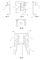
Fig. 1 is a front view of an electromagnetic shielding cover according to the first embodiment of the present invention; -
Fig. 2 is a right side view of an electromagnetic shielding cover according to the first embodiment of the present invention; -
Fig. 3 is a top view of an electromagnetic shielding cover according to the first embodiment of the present invention; -
Fig. 4 is a front view of a wiring frame according to the first embodiment of the present invention; -
Fig. 5 is a front view showing the implementation of the first embodiment of the present invention; -
Fig. 6 is a right side view showing the implementation of the first embodiment of the present invention; -
Fig. 7 is a top view showing the implementation of the first embodiment of the present invention; -
Fig. 8 is a front view of an electromagnetic shielding cover according to the second embodiment of the present invention; -
Fig. 9 is a right side view of an electromagnetic shielding cover according to the second embodiment of the present invention; -
Fig. 10 is a top view of an electromagnetic shielding cover according to the second embodiment of the present invention; -
Fig. 11 is a front view of a wiring frame according to the second embodiment of the present invention; -
Fig. 12 is a front view showing the implementation of the second embodiment of the present invention; -
Fig. 13 is a right side view showing the implementation of the second embodiment of the present invention; -
Fig. 14 is a top view showing the implementation of the second embodiment of the present invention; -
Fig. 15 is a front view of an electromagnetic shielding cover according to the third embodiment of the present invention; -
Fig. 16 is a right side view of an electromagnetic shielding cover according to the third embodiment of the present invention; -
Fig. 17 is a left side view of an electromagnetic shielding cover according to the third embodiment of the present invention; -
Fig. 18 is a bottom view of an electromagnetic shielding cover according to the third embodiment of the present invention; -
Fig. 19 is a front view showing a wiring frame of the third embodiment of the present invention; -
Fig. 20 is a top view showing the implementation of the third embodiment of the present invention; -
Fig. 21 is a front view showing the implementation of the third embodiment of the present invention; -
Fig. 22 is a left side view showing the implementation of the third embodiment of the present invention; -
Fig. 23 is a right side view showing the implementation of the third embodiment of the present invention; and -
Fig. 24 is a bottom view showing the implementation of the third embodiment of the present invention. - The embodiments of the present invention will be described in details by reference to the accompanying drawings.
- With reference to
Figs. 1 to 3 , according to the first embodiment of the present invention, there is awindow 2 in theelectromagnetic shielding cover 1, and ashielding net 3 is provided in thewindow 2. Theelectromagnetic shielding cover 1 has a protrudingtongue 6 in the bottom of its both sides respectively. The protrudingtongues 6 have two bends of 90° respectively, and are in a trapezoid shape. - With reference to
Fig. 4 , awiring frame 4 is formed with twopositioning notches 5 on its both sides. A receivingdiode chip 10 and anIC chip 11 are mounted in thewiring frame 4. Herein, the receivingdiode chip 10 and theIC chip 11 are connected with functional circuits of the household electrical appliances, etc. vialeads 12. Thewiring frame 4 can be of pure metal, and can also be other types of wiring frames of copper-coated plate, metallized ceramic, and the like. - With reference to
Figs. 5 to 7 , the two protrudingtongues 6 of theelectromagnetic shielding cover 1 are engaged with the twopositioning notches 5 of thewiring frame 4. The protrudingtongues 6 are bent downwards and entad to engage on thewiring frame 4, thus forming an electromagnetic shielding structure transparent to thechips - In the first embodiment of the present invention, the horizontal and longitudinal beams forming the shielding net 3 can be of structure integral with the
electromagnetic shielding cover 1, and can also be any other structure attached to theelectromagnetic shielding cover 1 by processes well-known to those skilled in the art. - In addition, the
window 2 and the shielding net 3 are not limited to the forms discussed above. Thewindow 2 can be divided into more windows with smaller size, and the shielding net 3 can also have more beams intersecting with each other in the horizontal and longitudinal directions. - Furthermore, the beams of the shielding net 3 which intersect with each other are not limited to intersection in the horizontal and longitudinal directions, but they can also intersect in oblique directions.
- In the present invention, the bend of the protruding tongue is not limited to 90°, but it can be of any other angle that can fix the
electromagnetic shielding cover 1 to thewiring frame 4. For example, the angle may be within a range of 30° to 150°. - With reference to
Figs. 8 to 10 , according to the second embodiment of the present invention, there is awindow 2 in theelectromagnetic shielding cover 1, and a shielding net 3 is provided in thewindow 2. Theelectromagnetic shielding cover 1 has a protrudingtongue 6 in the bottom of its both sides respectively. The protrudingtongues 6 have no bends and are in a planar shape. - With reference to
Fig. 11 , thewiring frame 4 is formed with twopositioning notches 5 on its both sides. A receiving diode chip and an IC chip (which are similar with those in the first embodiment and not shown here) are mounted in thewiring frame 4. Herein, the receiving diode chip and the IC chip are connected with functional circuits of the household electrical appliances, etc. via leads 12. Thewiring frame 4 can be of pure metal, and can also be other types of wiring frames of copper-coated plate, metallized ceramic, and the like. - With reference to
Figs. 12 to 14 , the two protrudingtongues 6 of theelectromagnetic shielding cover 1 are engaged with the twopositioning notches 5 of thewiring frame 4. The protrudingtongues 6 are bent downwards and entad to engage on thewiring frame 4, thus forming an electromagnetic shielding structure transparent to the chips inside. - In the second embodiment of the present invention, the horizontal and longitudinal beams forming the shielding net 3 can be of structure integral with the
electromagnetic shielding cover 1, and can also be any other structure attached to theelectromagnetic shielding cover 1 by processes well-known to those skilled in the art. - In addition, the
window 2 and the shielding net 3 are not limited to the forms discussed above. Thewindow 2 can be divided into more windows with smaller size, and the shielding net 3 can also have more beams intersecting with each other in the horizontal and longitudinal directions. - Furthermore, the beams of the shielding net 3 which intersect with each other are not limited to intersection in the horizontal and longitudinal directions, but they can also intersect in oblique directions.
- With reference to
Figs. 15 to 18 , according to the third embodiment of the present invention, there is awindow 2 in the metalelectromagnetic shielding cover 1, and a shielding net 3 is provided in thewindow 2. The metalelectromagnetic shielding cover 1 has an "n" shape protruding lugs in the bottom of its both sides respectively. The "n" shape protruding lugs branch into a long valvule and a short one. Thelong valvule 7 bends toward the short one to engage on thewiring frame 4. Besides, the metal electromagnetic shielding cover has in its bottom a tongue-shapedpart 8. - With reference to
Fig. 19 , thewiring frame 4 is formed with twopositioning notches 5 on its upper sides for fixing the "n" shape protruding lugs of theelectromagnetic shielding cover 1. There is an "L"shape slot 9 in the center of thewiring frame 4, which engages with the tongue-shapedpart 8 of theelectromagnetic shielding cover 1 to position theelectromagnetic shielding cover 1. A receiving diode chip and an IC chip are mounted in thewiring frame 4. The receiving diode chip and the IC chip are connected with functional circuits of the household electrical appliances, etc. via leads 12. Thewiring frame 4 can be of pure metal, and can also be other types of wiring frames of copper-coated plate, metallized ceramic, and the like. - With reference to
Figs. 20 to 24 , the twolong valvules 7 of the metalelectromagnetic shielding cover 1 are engaged with the twopositioning notches 5 of thewiring frame 4. During assembling, thelong valvules 7 are bent toward the short valvules to engage on thewiring frame 4, and the tongue-shapedpart 8 of the metalelectromagnetic shielding cover 1 are engaged with the "L"shape slot 9 of thewiring frame 4. As a result, an electromagnetic shielding structure transparent to thechip 10 andchip 11 inside is formed. - As shown in
Figs. 16 and 17 , thelong valvules 7 of the two "n" shape protruding lugs for theelectromagnetic shielding cover 1 are provided at opposite sides, to facilitate firmly fixing theelectromagnetic shielding cover 1 to thewiring frame 4. - In addition, in the third embodiment of the present invention, the
long valvules 7 of the two "n" shape protruding lugs for theelectromagnetic shielding cover 1 can be long enough so as to wrap thepositioning notches 5 of thewiring frame 4 one cycle, i.e. to enclose thepositioning notches 5 in a closed structure formed by thelong valvules 7 and the short valvules. In this manner, thelong valvules 7 of the two "n" shape protruding lugs can be provided at the same side (not shown), i.e. thelong valvules 7 can be both at the upper side of the "n" shape protruding lugs, or both at the lower side of the "n" shape protruding lugs. - Furthermore, in the third embodiment of the present invention, the horizontal and longitudinal beams forming the shielding net 3 can be of structure integral with the
electromagnetic shielding cover 1, and can also be any other structure attached to theelectromagnetic shielding cover 1 by processes well-known to those skilled in the art. - In addition, the
window 2 and the shielding net 3 are not limited to the forms discussed above. Thewindow 2 can be divided into more windows with smaller size, and the shielding net 3 can also have more beams intersecting with each other in the horizontal and longitudinal directions. - Furthermore, the beams of the shielding net 3 which intersect with each other are not limited to intersection in the horizontal and longitudinal directions, but they can also intersect in oblique directions.
- In the third embodiment of the present invention, the bends of the two valvules for the "n" shape protruding lugs can be of any angle that can fix the
electromagnetic shielding cover 1 to thewiring frame 4. For example, the angle may be within a range of 30° to 150°. - The electromagnetic shielding device of the present invention is simple in structure, reasonable in design, easy to manufacture, low-cost, high qualified ratio and thus suitable for mass productivity. The electromagnetic shielding device improves the electromagnetic interference preventive capability of a semiconductor element and thus increases the sensibility and reliability of the infrared receiver.
- Although the specific descriptions are provided for the embodiments of the present invention, but they are not exhaustive and not limit the invention to those disclosed forms. Based on the above description, those skilled in the art can make various modifications and/or changes without departing from the spirit and scope of the present invention.
Claims (12)
- An electromagnetic shielding device within an infrared receiver, which comprises of a wiring frame (4) and an electromagnetic shielding cover (1), wherein there being in the electromagnetic shielding cover (1) a window (2) in which there provided a shielding net (3), characterized in that: the electromagnetic shielding cover (1) having a protruding tongue (6) in the bottom of its both sides respectively, and the protruding tongues (6) bent downwards and entad to engage on the wiring frame (4), thus forming an electromagnetic shielding structure transparent to the chip (10, 11) inside.
- The electromagnetic shielding device according to claim 1, wherein the wiring frame (4) is formed with two positioning notches (5) on its both sides, and the protruding tongues (6) are engaged on the positioning notches (5).
- The electromagnetic shielding device according to claim 1, wherein the window (2) includes a plurality of windows, and the shielding net is consisted of a plurality of intersecting beams.
- The electromagnetic shielding device according to claim 1, wherein the beams are of structure integral with the electromagnetic shielding cover (1), or any other structure attached to the electromagnetic shielding cover (1).
- The electromagnetic shielding device according to claim 1, wherein the protruding tongues (6) are in a flat shape.
- The electromagnetic shielding device according to claim 1, wherein each of the protruding tongues (6) has two bends.
- An electromagnetic shielding device within an infrared receiver, which comprises of a wiring frame (4), semiconductor chips (10, 11) mounted on the wiring frame (4), and an electromagnetic shielding cover (1), wherein there is a window (2) in the electromagnetic shielding cover (1), in which there is provided a shielding net (3), characterized in that: the electromagnetic shielding cover (1) has an "n" shape protruding lugs in the bottom of its both sides respectively, and each "n" shape protruding lug has a long valvule (7) at the lower part, the long valvule (7) being bent to the short valvule side to engage on the wiring frame (4), thus forming an electromagnetic shielding structure transparent to the chips (10, 11) inside.
- The electromagnetic shielding device according to claim 7, wherein the electromagnetic shielding cover (1) has a tongue-shaped part (8) at the lower part, and the tongue-shaped part (8) is connected with an "L" shape slot (9) of the wiring frame (4).
- The electromagnetic shielding device according to claim 7, wherein the wiring frame (4) has two positioning notches (5) on the upper part, and the "n" shape protruding lugs are engaged on the positioning notches (5).
- The electromagnetic shielding device according to claim 7, wherein the window (2) includes a plurality of windows, and the shielding net is consisted of a plurality of intersecting beams.
- The electromagnetic shielding device according to claim 7, wherein the beams are of structure integral with the electromagnetic shielding cover (1), or any other structure attached to the electromagnetic shielding cover (1).
- The electromagnetic shielding device according to claim 7, wherein the long valvules (7) in the bottom of both sides of the electromagnetic shielding device (1) are located on the opposite sides, or on the same sides.
Applications Claiming Priority (3)
| Application Number | Priority Date | Filing Date | Title |
|---|---|---|---|
| CN200520022019 | 2005-11-25 | ||
| CN200620020197.6U CN2911964Y (en) | 2006-02-13 | 2006-02-13 | Electromagnetic shielding device for infrared receiver |
| PCT/CN2006/003120 WO2007059700A1 (en) | 2005-11-25 | 2006-11-20 | An electromagnetic shielding device for an infrared receiver |
Publications (2)
| Publication Number | Publication Date |
|---|---|
| EP1959720A1 true EP1959720A1 (en) | 2008-08-20 |
| EP1959720A4 EP1959720A4 (en) | 2011-03-30 |
Family
ID=38066917
Family Applications (1)
| Application Number | Title | Priority Date | Filing Date |
|---|---|---|---|
| EP06817858A Withdrawn EP1959720A4 (en) | 2005-11-25 | 2006-11-20 | ELECTROMAGNETIC SHIELDING DEVICE FOR AN INFRARED RECEIVER |
Country Status (3)
| Country | Link |
|---|---|
| US (1) | US7952157B2 (en) |
| EP (1) | EP1959720A4 (en) |
| WO (1) | WO2007059700A1 (en) |
Families Citing this family (1)
| Publication number | Priority date | Publication date | Assignee | Title |
|---|---|---|---|---|
| CN106935663B (en) * | 2017-02-24 | 2018-06-29 | 江苏欧密格光电科技股份有限公司 | A kind of patch infrared receiving terminal |
Family Cites Families (7)
| Publication number | Priority date | Publication date | Assignee | Title |
|---|---|---|---|---|
| JPH08222746A (en) * | 1995-02-15 | 1996-08-30 | Fujitsu Ltd | Infrared detector |
| JP2000252680A (en) * | 1999-03-04 | 2000-09-14 | Sharp Corp | Light receiving unit |
| JP2004087953A (en) * | 2002-08-28 | 2004-03-18 | Tokai Rubber Ind Ltd | Electronic equipment housing |
| CN2610574Y (en) * | 2003-02-08 | 2004-04-07 | 杨家象 | Shield in infrared receiver |
| KR20050048701A (en) * | 2003-11-19 | 2005-05-25 | 조인셋 주식회사 | Multi-functional metal shield case and method for making the same |
| CN1662129A (en) * | 2004-02-27 | 2005-08-31 | 乐金电子(沈阳)有限公司 | Structure of shield cover in use for receiver of remote control signal |
| JP2005347632A (en) * | 2004-06-04 | 2005-12-15 | Sharp Corp | Semiconductor device and electronic equipment |
-
2006
- 2006-11-20 WO PCT/CN2006/003120 patent/WO2007059700A1/en not_active Ceased
- 2006-11-20 US US12/093,204 patent/US7952157B2/en not_active Expired - Fee Related
- 2006-11-20 EP EP06817858A patent/EP1959720A4/en not_active Withdrawn
Also Published As
| Publication number | Publication date |
|---|---|
| EP1959720A4 (en) | 2011-03-30 |
| US7952157B2 (en) | 2011-05-31 |
| WO2007059700A1 (en) | 2007-05-31 |
| US20080283976A1 (en) | 2008-11-20 |
Similar Documents
| Publication | Publication Date | Title |
|---|---|---|
| US7026654B2 (en) | Package for optical semiconductor | |
| EP2062301B1 (en) | Housing for an optoelectronic component and arrangement of an optoelectronic component in the housing | |
| US10062994B2 (en) | Electrical connector | |
| CN214123875U (en) | Infrared receiving head | |
| US7952157B2 (en) | Electromagnetic shielding device for an infrared receiver | |
| WO2011015667A1 (en) | One-piece shielding hood with one or more pins | |
| HK1120704A (en) | An electromagnetic shielding device for an infrared receiver | |
| US7791084B2 (en) | Package with overlapping devices | |
| US20130288503A1 (en) | Card edge connector with floating metal member | |
| JP4813691B2 (en) | Light emitting diode | |
| US6489555B1 (en) | Elastic system for preventing electromagnetic interference to a computer central processing unit | |
| CN208044239U (en) | Electronic equipment | |
| US20110248136A1 (en) | Protruding positioning pedestal | |
| JP2002252357A (en) | Photoelectric sensor | |
| JPH0710502Y2 (en) | Light receiving device for remote control | |
| JP2598381Y2 (en) | Remote control light receiving module | |
| JP2602796Y2 (en) | Receiver module for infrared remote control | |
| KR20150095371A (en) | Double contact terminal on the board | |
| CN207689781U (en) | A kind of metal frame and liquid crystal display die set | |
| KR20100039987A (en) | Receiving module of remote control and mounting structure thereof | |
| JPS58199575A (en) | Photoelectric device | |
| CN211743154U (en) | Photoelectric converter | |
| US20240178329A1 (en) | Semiconductor packages with side-facing ambient light sensors | |
| CN201060867Y (en) | An electromagnetic inner shielding device for an infrared receiver | |
| CN2911964Y (en) | Electromagnetic shielding device for infrared receiver |
Legal Events
| Date | Code | Title | Description |
|---|---|---|---|
| PUAI | Public reference made under article 153(3) epc to a published international application that has entered the european phase |
Free format text: ORIGINAL CODE: 0009012 |
|
| 17P | Request for examination filed |
Effective date: 20080616 |
|
| AK | Designated contracting states |
Kind code of ref document: A1 Designated state(s): DE FR GB |
|
| RBV | Designated contracting states (corrected) |
Designated state(s): DE FR GB |
|
| REG | Reference to a national code |
Ref country code: HK Ref legal event code: DE Ref document number: 1120704 Country of ref document: HK |
|
| DAX | Request for extension of the european patent (deleted) | ||
| A4 | Supplementary search report drawn up and despatched |
Effective date: 20110224 |
|
| RIC1 | Information provided on ipc code assigned before grant |
Ipc: H01L 23/552 20060101ALI20110218BHEP Ipc: H01L 27/146 20060101ALI20110218BHEP Ipc: H05K 9/00 20060101AFI20070726BHEP Ipc: H01L 31/0203 20060101ALI20110218BHEP |
|
| 17Q | First examination report despatched |
Effective date: 20110915 |
|
| REG | Reference to a national code |
Ref country code: HK Ref legal event code: WD Ref document number: 1120704 Country of ref document: HK |
|
| STAA | Information on the status of an ep patent application or granted ep patent |
Free format text: STATUS: THE APPLICATION IS DEEMED TO BE WITHDRAWN |
|
| 18D | Application deemed to be withdrawn |
Effective date: 20160601 |