EP1959568A1 - Thin-film bulk acoustic ware resonator and method for performing heterogeneous integration of the same with complementary-metal-oxide-semiconductor integrated circuit - Google Patents
Thin-film bulk acoustic ware resonator and method for performing heterogeneous integration of the same with complementary-metal-oxide-semiconductor integrated circuit Download PDFInfo
- Publication number
- EP1959568A1 EP1959568A1 EP07380041A EP07380041A EP1959568A1 EP 1959568 A1 EP1959568 A1 EP 1959568A1 EP 07380041 A EP07380041 A EP 07380041A EP 07380041 A EP07380041 A EP 07380041A EP 1959568 A1 EP1959568 A1 EP 1959568A1
- Authority
- EP
- European Patent Office
- Prior art keywords
- fbar
- device chip
- chip including
- substrate
- metal electrode
- Prior art date
- Legal status (The legal status is an assumption and is not a legal conclusion. Google has not performed a legal analysis and makes no representation as to the accuracy of the status listed.)
- Withdrawn
Links
- 239000010409 thin film Substances 0.000 title claims abstract description 36
- 238000000034 method Methods 0.000 title claims description 62
- 230000010354 integration Effects 0.000 title claims description 29
- 239000004065 semiconductor Substances 0.000 title description 3
- 239000000758 substrate Substances 0.000 claims abstract description 79
- 229910052751 metal Inorganic materials 0.000 claims abstract description 47
- 239000002184 metal Substances 0.000 claims abstract description 47
- 238000007667 floating Methods 0.000 claims abstract description 10
- 238000004519 manufacturing process Methods 0.000 claims description 28
- 238000005516 engineering process Methods 0.000 claims description 18
- 230000008021 deposition Effects 0.000 claims description 9
- 238000005530 etching Methods 0.000 claims description 9
- XUIMIQQOPSSXEZ-UHFFFAOYSA-N Silicon Chemical compound [Si] XUIMIQQOPSSXEZ-UHFFFAOYSA-N 0.000 claims description 6
- 239000010703 silicon Substances 0.000 claims description 6
- 229910052710 silicon Inorganic materials 0.000 claims description 6
- 229910001218 Gallium arsenide Inorganic materials 0.000 claims 1
- 239000004020 conductor Substances 0.000 claims 1
- 239000010410 layer Substances 0.000 description 32
- 230000008569 process Effects 0.000 description 22
- 238000005476 soldering Methods 0.000 description 11
- 239000000463 material Substances 0.000 description 10
- 238000000151 deposition Methods 0.000 description 9
- BASFCYQUMIYNBI-UHFFFAOYSA-N platinum Chemical compound [Pt] BASFCYQUMIYNBI-UHFFFAOYSA-N 0.000 description 7
- 239000011241 protective layer Substances 0.000 description 7
- 235000012431 wafers Nutrition 0.000 description 7
- PXHVJJICTQNCMI-UHFFFAOYSA-N Nickel Chemical compound [Ni] PXHVJJICTQNCMI-UHFFFAOYSA-N 0.000 description 6
- 238000013459 approach Methods 0.000 description 6
- 239000010931 gold Substances 0.000 description 6
- 238000004806 packaging method and process Methods 0.000 description 6
- 229910052737 gold Inorganic materials 0.000 description 5
- 239000010936 titanium Substances 0.000 description 5
- RTAQQCXQSZGOHL-UHFFFAOYSA-N Titanium Chemical compound [Ti] RTAQQCXQSZGOHL-UHFFFAOYSA-N 0.000 description 4
- 229910052782 aluminium Inorganic materials 0.000 description 4
- XAGFODPZIPBFFR-UHFFFAOYSA-N aluminium Chemical compound [Al] XAGFODPZIPBFFR-UHFFFAOYSA-N 0.000 description 4
- 239000011651 chromium Substances 0.000 description 4
- PMHQVHHXPFUNSP-UHFFFAOYSA-M copper(1+);methylsulfanylmethane;bromide Chemical compound Br[Cu].CSC PMHQVHHXPFUNSP-UHFFFAOYSA-M 0.000 description 4
- PCHJSUWPFVWCPO-UHFFFAOYSA-N gold Chemical compound [Au] PCHJSUWPFVWCPO-UHFFFAOYSA-N 0.000 description 4
- 229910052719 titanium Inorganic materials 0.000 description 4
- 230000008878 coupling Effects 0.000 description 3
- 238000010168 coupling process Methods 0.000 description 3
- 238000005859 coupling reaction Methods 0.000 description 3
- 238000002955 isolation Methods 0.000 description 3
- 229910052759 nickel Inorganic materials 0.000 description 3
- 229910052697 platinum Inorganic materials 0.000 description 3
- 229910052715 tantalum Inorganic materials 0.000 description 3
- GUVRBAGPIYLISA-UHFFFAOYSA-N tantalum atom Chemical compound [Ta] GUVRBAGPIYLISA-UHFFFAOYSA-N 0.000 description 3
- 238000012546 transfer Methods 0.000 description 3
- 238000001039 wet etching Methods 0.000 description 3
- VYZAMTAEIAYCRO-UHFFFAOYSA-N Chromium Chemical compound [Cr] VYZAMTAEIAYCRO-UHFFFAOYSA-N 0.000 description 2
- ZOKXTWBITQBERF-UHFFFAOYSA-N Molybdenum Chemical compound [Mo] ZOKXTWBITQBERF-UHFFFAOYSA-N 0.000 description 2
- 239000012814 acoustic material Substances 0.000 description 2
- 239000003990 capacitor Substances 0.000 description 2
- 229910052804 chromium Inorganic materials 0.000 description 2
- 238000010276 construction Methods 0.000 description 2
- 238000011161 development Methods 0.000 description 2
- 230000018109 developmental process Effects 0.000 description 2
- 229910052451 lead zirconate titanate Inorganic materials 0.000 description 2
- 150000002739 metals Chemical class 0.000 description 2
- 238000005459 micromachining Methods 0.000 description 2
- 238000012986 modification Methods 0.000 description 2
- 230000004048 modification Effects 0.000 description 2
- 229910052750 molybdenum Inorganic materials 0.000 description 2
- 239000011733 molybdenum Substances 0.000 description 2
- 238000012805 post-processing Methods 0.000 description 2
- 230000001681 protective effect Effects 0.000 description 2
- WFKWXMTUELFFGS-UHFFFAOYSA-N tungsten Chemical compound [W] WFKWXMTUELFFGS-UHFFFAOYSA-N 0.000 description 2
- 229910052721 tungsten Inorganic materials 0.000 description 2
- 239000010937 tungsten Substances 0.000 description 2
- KRHYYFGTRYWZRS-UHFFFAOYSA-N Fluorane Chemical compound F KRHYYFGTRYWZRS-UHFFFAOYSA-N 0.000 description 1
- 229910000990 Ni alloy Inorganic materials 0.000 description 1
- 229910000978 Pb alloy Inorganic materials 0.000 description 1
- OAICVXFJPJFONN-UHFFFAOYSA-N Phosphorus Chemical compound [P] OAICVXFJPJFONN-UHFFFAOYSA-N 0.000 description 1
- 101100460147 Sarcophaga bullata NEMS gene Proteins 0.000 description 1
- VYPSYNLAJGMNEJ-UHFFFAOYSA-N Silicium dioxide Chemical compound O=[Si]=O VYPSYNLAJGMNEJ-UHFFFAOYSA-N 0.000 description 1
- XLOMVQKBTHCTTD-UHFFFAOYSA-N Zinc monoxide Chemical compound [Zn]=O XLOMVQKBTHCTTD-UHFFFAOYSA-N 0.000 description 1
- 239000000853 adhesive Substances 0.000 description 1
- 230000001070 adhesive effect Effects 0.000 description 1
- 229910045601 alloy Inorganic materials 0.000 description 1
- 239000000956 alloy Substances 0.000 description 1
- 239000000919 ceramic Substances 0.000 description 1
- 238000001816 cooling Methods 0.000 description 1
- 238000013461 design Methods 0.000 description 1
- 238000009713 electroplating Methods 0.000 description 1
- 230000001747 exhibiting effect Effects 0.000 description 1
- 239000011521 glass Substances 0.000 description 1
- 238000010438 heat treatment Methods 0.000 description 1
- 229960002050 hydrofluoric acid Drugs 0.000 description 1
- HFGPZNIAWCZYJU-UHFFFAOYSA-N lead zirconate titanate Chemical compound [O-2].[O-2].[O-2].[O-2].[O-2].[Ti+4].[Zr+4].[Pb+2] HFGPZNIAWCZYJU-UHFFFAOYSA-N 0.000 description 1
- 238000001465 metallisation Methods 0.000 description 1
- 238000000206 photolithography Methods 0.000 description 1
- 238000000623 plasma-assisted chemical vapour deposition Methods 0.000 description 1
- 238000001552 radio frequency sputter deposition Methods 0.000 description 1
- 230000009467 reduction Effects 0.000 description 1
- 230000004044 response Effects 0.000 description 1
- 239000005368 silicate glass Substances 0.000 description 1
- 229910052814 silicon oxide Inorganic materials 0.000 description 1
- 229910000679 solder Inorganic materials 0.000 description 1
- 239000000243 solution Substances 0.000 description 1
- 239000000126 substance Substances 0.000 description 1
- 238000012360 testing method Methods 0.000 description 1
Images


Classifications
-
- H—ELECTRICITY
- H03—ELECTRONIC CIRCUITRY
- H03H—IMPEDANCE NETWORKS, e.g. RESONANT CIRCUITS; RESONATORS
- H03H9/00—Networks comprising electromechanical or electro-acoustic elements; Electromechanical resonators
- H03H9/15—Constructional features of resonators consisting of piezoelectric or electrostrictive material
- H03H9/17—Constructional features of resonators consisting of piezoelectric or electrostrictive material having a single resonator
- H03H9/171—Constructional features of resonators consisting of piezoelectric or electrostrictive material having a single resonator implemented with thin-film techniques, i.e. of the film bulk acoustic resonator [FBAR] type
- H03H9/172—Means for mounting on a substrate, i.e. means constituting the material interface confining the waves to a volume
-
- B—PERFORMING OPERATIONS; TRANSPORTING
- B81—MICROSTRUCTURAL TECHNOLOGY
- B81C—PROCESSES OR APPARATUS SPECIALLY ADAPTED FOR THE MANUFACTURE OR TREATMENT OF MICROSTRUCTURAL DEVICES OR SYSTEMS
- B81C1/00—Manufacture or treatment of devices or systems in or on a substrate
- B81C1/00015—Manufacture or treatment of devices or systems in or on a substrate for manufacturing microsystems
- B81C1/00222—Integrating an electronic processing unit with a micromechanical structure
- B81C1/00238—Joining a substrate with an electronic processing unit and a substrate with a micromechanical structure
-
- H—ELECTRICITY
- H03—ELECTRONIC CIRCUITRY
- H03H—IMPEDANCE NETWORKS, e.g. RESONANT CIRCUITS; RESONATORS
- H03H3/00—Apparatus or processes specially adapted for the manufacture of impedance networks, resonating circuits, resonators
- H03H3/007—Apparatus or processes specially adapted for the manufacture of impedance networks, resonating circuits, resonators for the manufacture of electromechanical resonators or networks
- H03H3/02—Apparatus or processes specially adapted for the manufacture of impedance networks, resonating circuits, resonators for the manufacture of electromechanical resonators or networks for the manufacture of piezoelectric or electrostrictive resonators or networks
-
- H—ELECTRICITY
- H03—ELECTRONIC CIRCUITRY
- H03H—IMPEDANCE NETWORKS, e.g. RESONANT CIRCUITS; RESONATORS
- H03H9/00—Networks comprising electromechanical or electro-acoustic elements; Electromechanical resonators
- H03H9/02—Details
- H03H9/05—Holders or supports
- H03H9/0538—Constructional combinations of supports or holders with electromechanical or other electronic elements
- H03H9/0547—Constructional combinations of supports or holders with electromechanical or other electronic elements consisting of a vertical arrangement
-
- B—PERFORMING OPERATIONS; TRANSPORTING
- B81—MICROSTRUCTURAL TECHNOLOGY
- B81B—MICROSTRUCTURAL DEVICES OR SYSTEMS, e.g. MICROMECHANICAL DEVICES
- B81B2201/00—Specific applications of microelectromechanical systems
- B81B2201/02—Sensors
- B81B2201/0271—Resonators; ultrasonic resonators
-
- B—PERFORMING OPERATIONS; TRANSPORTING
- B81—MICROSTRUCTURAL TECHNOLOGY
- B81C—PROCESSES OR APPARATUS SPECIALLY ADAPTED FOR THE MANUFACTURE OR TREATMENT OF MICROSTRUCTURAL DEVICES OR SYSTEMS
- B81C2201/00—Manufacture or treatment of microstructural devices or systems
- B81C2201/01—Manufacture or treatment of microstructural devices or systems in or on a substrate
- B81C2201/0174—Manufacture or treatment of microstructural devices or systems in or on a substrate for making multi-layered devices, film deposition or growing
- B81C2201/019—Bonding or gluing multiple substrate layers
Definitions
- the present invention relates to acoustic resonators and its fabrication, to integrated circuits and its fabrication; and more particularly to the combination of the above techniques and methods for performing heterogeneous integration of thin-film bulk acoustic wave resonators (FBAR) with complementary-metal-oxide-semiconductor (CMOS) integrated circuit (IC).
- FBAR thin-film bulk acoustic wave resonators
- CMOS complementary-metal-oxide-semiconductor
- MEMS micro-electromechanical systems
- FBAR thin-film bulk acoustic wave resonators
- Second approach for FBAR-to-CMOS is to monolithically integrate FBAR with CMOS circuitry.
- FBAR is placed above the circuit, in order to save die area.
- This approach was disclosed in late 1993 [12], even a system integrating FBAR and radio circuitry was conceived in 2001 [13]. However, it was not as late as 2005 when the first monolithic FBAR-above-IC systems were demonstrated [14-16].
- the interest for monolithic integration of FBAR has not limited to full-active ICs, but also for passive components like CMOS inductors [17].
- Other MEMS, NEMS and SAW integrated resonators have been demonstrated, as well [18-20].
- CMOS substrate may be transferred to FBAR substrate.
- this approach implements various techniques additional to standard CMOS and FBAR fabrication, including flip-chip, multi-chip-module, surface micromachining and packaging.
- some of these techniques are utilized in a different way to the standard application.
- packaging of MEMS or FBAR has traditionally been implemented as a protective means of device [21-24], where caps and protective structures are provided to enclose the device.
- a method for packaging FBAR is presented, where a device chip having circuit elements and a cap is fabricated. To complete the process, the cap is placed on the device chip to connect a first contact point with a second contact point using the connector on the cap.
- a reduced substrate MEMS device and system for producing the same is disclosed in [26].
- a process in accordance with embodiments of the invention may include bonding a first packaging part to a MEMS device including a support substrate, removing the support substrate, and bonding a second packaging part to the MEMS device. Also related with reducing losses due to substrate coupling, a method for fabricating a floating FBAR structure has been disclosed in [27].
- the thin film resonator includes a supporting means, a first electrode, a dielectric layer, and a second electrode.
- the FBAR supporting layer has posts and a supporting layer formed on the posts, yet comprising a three dimensional, floating construction.
- the supporting layer and posts are fabricated by means of surface micro-machining of a sacrificial layer.
- the overall structure is still supported on isolating substrate material such as silicon, glass or ceramic.
- the FBAR is a three-dimensional, floating structure.
- the whole FBAR structure of the present invention is completely transferred to a supporting substrate, with no presence of sacrificial layer in the target substrate. Hence, no etching of the FBAR supporting substrate is needed.
- the FBAR is exclusively supported by two or more posts. This reduces the number of steps and time involved in the fabrication of the FBAR.
- the supporting posts may be connecting points to a CMOS substrate, allowing for heterogeneous integration of FBAR-to-CMOS, being the FBAR placed above the integrated circuit. This means that die area may be reduced, compared to hybrid or even to FBAR-on-side-of-IC monolithic integration. This implies that no specific technology development is needed in order to provide with technologic compatibility to both FBAR and CMOS fabrication processes.
- FBAR thin-film bulk acoustic wave resonator
- FBAR thin-film bulk acoustic wave resonator
- FBAR thin-film bulk acoustic wave resonator
- FBAR thin-film bulk acoustic wave resonator
- FBAR thin-film bulk acoustic wave resonator
- FBAR thin-film bulk acoustic wave resonator
- CMOS complementary metal-oxide-semiconductor
- FBAR thin-film bulk acoustic wave resonator
- CMOS complementary-metal-oxide-semiconductor
- Said connecting points provide the FBAR-to-IC integration and may be implemented as soldering bumps, thru-hole or via-hole-fabricated supporting posts, or electro-plating deposition.
- This invention is understood to not be limited to FBAR devices, and its principles may be applied to other suitable MEMS devices.
- MEMS device may be understood to include, inter alia, any suitable micro-electromechanical system device, for example, a thin-film bulk acoustic resonator (FBAR), an FBAR filter, and FBAR RF filter, a RF switch, a varactor, a tunable capacitor, or any other MEMS device where it may be relevant to apply the principles of the present invention.
- FBAR thin-film bulk acoustic resonator
- FBAR FBAR RF filter
- RF switch a varactor
- varactor a tunable capacitor
- an FBAR is placed on and connected to a CMOS substrate, thus configuring a floating structure on the substrate.
- the CMOS substrate may carry integrated circuitry, although this is not strictly necessary, being enough a CMOS substrate carrying connecting interfaces to the FBAR.
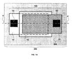
- FIG. 1A and FIG. 1B are schematics illustrating top and cross-sectional views of the integrated FBAR-to-CMOS 300, where FBAR 100 is placed on CMOS substrate 200.
- the only supporting means, making the FBAR 100 a three-dimensional, floating structure are the posts 14 and 15.
- posts 14 and 15 serve as connecting points, providing electrical contact between FBAR 100 and CMOS substrate 200.
- supporting substrate 200 may be a CMOS substrate carrying passive devices, dummy interconnections, test structures, integrated circuitry, or combinations of one or more of these.
- CMOS substrate carrying passive devices, dummy interconnections, test structures, integrated circuitry, or combinations of one or more of these.
- the present invention is not limited to CMOS technologies, being possible to apply the present invention to other integrated circuit technologies.
- an exemplary embodiment of the present invention includes CMOS technology as substrate 200 for providing support to FBAR 100.
- FBAR 100 is conformed by metal electrodes 11 and 13, and acoustic material thin-film 12.
- FIG. 1 B the air interface 350 between FBAR 100 and substrate 200 provides acoustical and mechanical isolation between FBAR and substrate, in order to guarantee a high quality factor. This air interface is the result of one of the fabrication processes described following.
- FIGs. 2A to 2D schematic description of the fabrication process of FBAR 100 is given, according to one embodiment of the present invention.
- a sacrificial layer 110 is deposited on top of the silicon substrate 119. Said sacrificial layer 110 will be released when FBAR 100 and substrate 200 are to be integrated. Other dielectric layers having similar properties to PSG may be implemented in other embodiments of the present invention.
- FIG. 2B The next step of the fabrication process of FBAR 100 is illustrated in FIG. 2B , where a metal electrode 111 is deposited on top of sacrificial layer 110.
- the material composing the metal electrode may be selected from the group of platinum, molybdenum, aluminum, gold, tungsten, tantalum, or any other having good electrical conductivity properties.
- this material is to provide crystallographic compatibility with the acoustical material to be used for implementation of the acoustic thin-film layer 112 in FIG.2C and 2D .
- acoustic material is deposited on top of the first metal electrode 111, which is made of one of the materials yet mentioned, or others with similar properties.
- the thin-film acoustic layer is deposited by means of RF sputtering, with no prejudice of other deposition or growing techniques, for example, epitaxial, or plasma-assisted deposition.
- CMOS technologies are not relevant to choose the thin-film acoustic layer, since FBAR 100 and substrate 200 are independent processes, being integrated just at the final step of the whole manufacturing process.
- the material composing the thin-film acoustic layer may be selected from the group of aluminum nitride (AIN), zinc-oxide (ZnO), lead zirconate titanate (PZT), lead tantalum zirconate titanate (PLZT), or any other material exhibiting good piezoelectric properties.
- FIG. 2D it is illustrated the last step of the FBAR 100 fabrication process, before integration to CMOS substrate, which is deposition of the second metal electrode 113.
- the material composing the metal electrode may be selected from the group of platinum, molybdenum, aluminum, gold, tungsten, tantalum, or any other having good electrical conductivity properties.
- Metal electrode 113 is deposited on top of the thin-film acoustical layer 112, and may be manufactured by the same processes carried-out to fabricate the first electrode.
- the FBAR 100 is provided with no air-interface or reflecting-mirror stack underneath the first metal electrode 111. Since air interface 350 will be provided in successive steps of the integration process, no additional steps are required for the FBAR 100 manufacturing process.
- FIG. 3 illustrates schematic of the cross-sectional view of an exemplary integrated-circuit process 211 fabricated on a carrying substrate 210.
- the integrated-circuit process 211 may be, but not restricted to, CMOS, being possible alternative implementations in bipolar, BiCMOS, SOI, or other integrated-circuit technologies.
- the integrated-circuit process may include a protective layer 212 on top of the remaining layers of the process. At its time, said protective layer 212 is provided with at least two opening windows 213 and 214 just above the top electrical conducting layer, or above of any other electrical conducting layer provided by the integrated-circuit technology.
- the opening windows 213 and 214 will serve as landing pads 215 and 216 to FBAR-to-CMOS interconnection.
- alternative configurations of the integrated-process may not include protective layer or opening windows on the latter.
- additional post-processing steps will be required in the integrated-circuit, in order to provide opening windows and protective layer on top of the integrated-circuit layers. Among these steps it may be implemented, inter alia, protective layer deposition and photolithography. Additional steps conducting to provide protective layer and opening windows on top of the integrated-circuit process will become apparent to those skilled in the art of integrated-circuit manufacturing.
- FIG. 4A schematic of the FBAR-to-CMOS heterogeneous integration process is illustrated for one embodiment of the present invention.
- deposition and etching of an alloy or stack of metals suitable for soldering or electro-platting is carried-out, thus defining landing pads 310 and 320.
- This step is required if metal electrodes 111 and 113 of FBAR 100 are not made of materials suitable to adherence for soldering or electro-platting purposes.
- the materials composing the landing pads 310 and 320 may be selected from the group of nickel, gold, titanium, among others.
- FIG.4B illustrates how connecting posts 330 and 340 are placed on top of landing pads 310 and 320.
- Connecting posts 330 and 340 will provide support and electrical connection to FBAR 100, giving to it the suspended configuration described in the preferred embodiment of the preferred invention.
- the techniques and methods required to implement posts 330 and 340 are diverse and include, inter alia, mask-driven deposition of soldering paste, metal deposition, and electro-platting assisted deposition.
- FIG. 4C is schematic describing the interconnection between FBAR and CMOS substrates. First, substrate 119 carrying FBAR 100 is vertically swapped and aligned to integrated-circuit substrate 200. This is done to provide alignment between connecting post 330 and opening window 213, and between connecting post 340 and opening window 214. The swapping and alignment procedures may be implemented by manual or automatic means.
- connecting posts 330 and 340 are soldering bumps that are heated and soldered to integrated-circuit pads 215 and 216, in one side, and to FBAR pads 310 and 320, in the other side.
- soldering may be replaced by electro-platting or deposition techniques, in order to achieve the interconnection described in FIG.4C .
- final release of FBAR is performed by wet etching of sacrificial layer 110, thus achieving complete integration between the FBAR 100 and the substrate 200. Since sacrificial layer 110 isolates FBAR 100 of substrate 119, the latter is also released when complete etching is achieved, separating both FBAR and substrate.
- FBAR 100 is fully released and connected to substrate 200, which may be an only supporting substrate or may carry passive or active devices.
- substrate 200 carries integrated-circuit devices, thus providing fully-integrated FBAR-to-CMOS application system 300.
- FBAR 100 exhibits two air interfaces, 350 and 360, respectively.
- FBAR 100 has mechanical freedom to vibrate since no acoustical coupling exists between it and any substrate. This fact is necessary condition to guarantee good quality factors.
- FBAR configuration may be as follows: a 1 ⁇ m-thick phosphor silicate glass (PSG) layer 110 is deposited on a 550 ⁇ m-thick silicon wafer. Next, a 180nm Cr/Pt (30nm of Cr for adhering purposes) is deposited and the first electrode 111 defined by lift-off. Afterwards, acoustic layer 112 is composed of a 1 ⁇ m-thick aluminum nitride (AIN) layer, being the resonator's shape defined by wet-etching. Finally, the second electrode 113 is made according to the same configuration of first electrode.
- PSG phosphor silicate glass
- AIN aluminum nitride
- CMOS substrate 200 may be fabricated according to the typical structure of a CMOS technology, i.e. a top metal layer 217 for interconnecting covered by a dielectric protective layer 212.
- This layer may be, for example, a 500nm-thick PECVD silicon oxide layer, with photolithography-defined openings 215 and 216 for pad connection.
- Metal layer 217 may be manufactured by one or more of the following configurations: platinum over chromium, aluminum over chromium, aluminum over titanium, among others. Possible metal configurations are mainly determined by the etchant solution implemented for subsequent FBAR-to-CMOS integration.
- FBAR-to-CMOS integration may be performed as follows: first, landing pads 310 and 320 may be selected from the group of nickel (Ni), gold (Au), titanium (Ti), or combination of two or all of them. For example, thicknesses for Ni, Au and Ti may be 30nm, 20nm and 50nm, respectively. If the top metal of CMOS technology does not provide with adhesive metals for interconnection with soldering bumps, similar procedure should also be practiced on top metal 217 of CMOS substrate. Next step is to place contacting posts 330 and 340 on top of landing pads 310 and 320. These posts may be soldering bumps, made of an alloy of nickel and lead (Pb).
- Pb nickel and lead
- soldering paste is applied to wafer by means of masking-aided appliance and alignment system.
- manual or automatic pick-and-place system may be used to position, align and soft contact FBAR and CMOS wafers in proper location.
- the ensemble is introduced in oven or heating machine, in order the soldering paste to liquefy and subsequent cooling to solder both endings of landing pads, allowing for hard interconnection between both FBAR and CMOS substrates.
- PSG layer 110 is attacked by means of HF-etching, releasing silicon substrate layer 119.
- FBAR exhibits full acoustic isolation by means of two air interfaces up and down of electrodes and, at the same time, full interconnection with CMOS substrate.
Landscapes
- Engineering & Computer Science (AREA)
- Manufacturing & Machinery (AREA)
- Physics & Mathematics (AREA)
- Acoustics & Sound (AREA)
- Microelectronics & Electronic Packaging (AREA)
- Piezo-Electric Or Mechanical Vibrators, Or Delay Or Filter Circuits (AREA)
Abstract
The present invention refers to a thin-film bulk acoustic wave resonator (FBAR) comprising:
- a first metal electrode;
- an acoustic layer;
- a second metal electrode;
- a carrier substrate;
- two or more supporting posts, said supporting posts connecting said first metal electrode and said second metal electrode to said carrier substrate;
said first metal electrode, said acoustic layer and said second metal electrode
arranged in a three-dimensional, floating structure, being said structure supported and interconnected to said carrier substrate by means of said supporting posts;
said first metal electrode interfacing in the vertical direction one of its surfaces withsaid acoustic layer and the second one with the air on top of said first metal electrode;
said acoustic layer interfacing in the vertical direction one of its surfaces with said first metal electrode and the second one with said second metal electrode;
said second metal electrode interfacing in the vertical direction one of its
surfaces with said acoustic layer and the second one with the air cavity formed in between said first metal electrode and said carrier substrate.
- a first metal electrode;
- an acoustic layer;
- a second metal electrode;
- a carrier substrate;
- two or more supporting posts, said supporting posts connecting said first metal electrode and said second metal electrode to said carrier substrate;
said first metal electrode, said acoustic layer and said second metal electrode
arranged in a three-dimensional, floating structure, being said structure supported and interconnected to said carrier substrate by means of said supporting posts;
said first metal electrode interfacing in the vertical direction one of its surfaces withsaid acoustic layer and the second one with the air on top of said first metal electrode;
said acoustic layer interfacing in the vertical direction one of its surfaces with said first metal electrode and the second one with said second metal electrode;
said second metal electrode interfacing in the vertical direction one of its
surfaces with said acoustic layer and the second one with the air cavity formed in between said first metal electrode and said carrier substrate.
Description
- The present invention relates to acoustic resonators and its fabrication, to integrated circuits and its fabrication; and more particularly to the combination of the above techniques and methods for performing heterogeneous integration of thin-film bulk acoustic wave resonators (FBAR) with complementary-metal-oxide-semiconductor (CMOS) integrated circuit (IC).
- The integration and process compatibility of micro-electromechanical systems (MEMS) to CMOS-integrated circuit technologies is one of the most demanding areas at both technology and application levels. Several issues like manufacturing temperature, packaging, and post-processing of MEMS; integrity of CMOS; and reliability and modeling of the MEMS-to-CMOS interface are just some examples that can be mentioned. The references presented in [1-3] describe some of the commented issues.
- As a micro-machined resonant system, thin-film bulk acoustic wave resonators (FBAR) have also attracted the attention of RF integrated-circuit and sensor-application designers, being capable of achieving high performance in radio-frequency (RF) and sensor applications, as well. The first FBAR was presented by Lakin and Wang in 1981 [4] and, since then, RF filters and duplexers [5], mass and chemical sensors [6-8], and other acoustic-based sensors have been investigated and manufactured.
- In considering the popularity and good response of FBAR, recent interest and latest developments in FBAR-to-CMOS integration have stimulated the conception of integrated applications in which FBAR is key component and whose IC integration is a requirement to proper functionality of the system. Different integration strategies have been investigated, being hybrid and monolithic integration the most relevant. By means of hybrid integration, two systems located in separated substrates are typically integrated by wire-bonding of the involved devices. In the case of FBAR-to-CMOS integration, the FBAR terminals are the bonding points of the first system to be connected, while the corresponding circuit nets do for the second system, in this case the IC. Examples of this integration approach are the oscillators presented in [9-11], where the FBAR performs thecrystal-like functionality in the system. Second approach for FBAR-to-CMOS is to monolithically integrate FBAR with CMOS circuitry. In the typical conception, FBAR is placed above the circuit, in order to save die area. This approach was disclosed in late 1993 [12], even a system integrating FBAR and radio circuitry was conceived in 2001 [13]. However, it was not as late as 2005 when the first monolithic FBAR-above-IC systems were demonstrated [14-16]. The interest for monolithic integration of FBAR has not limited to full-active ICs, but also for passive components like CMOS inductors [17]. Other MEMS, NEMS and SAW integrated resonators have been demonstrated, as well [18-20].
- At the date, hybrid or monolithic approaches are main-stream integration strategies. Now, a third integration approach introduced by the present invention is wafer-level-transfer of FBAR into CMOS substrate or, vice versa, CMOS substrate may be transferred to FBAR substrate. For this purpose, this approach implements various techniques additional to standard CMOS and FBAR fabrication, including flip-chip, multi-chip-module, surface micromachining and packaging. Implemented in this invention, some of these techniques are utilized in a different way to the standard application. For example, packaging of MEMS or FBAR has traditionally been implemented as a protective means of device [21-24], where caps and protective structures are provided to enclose the device. Also, in [25], a method for packaging FBAR is presented, where a device chip having circuit elements and a cap is fabricated. To complete the process, the cap is placed on the device chip to connect a first contact point with a second contact point using the connector on the cap. On the other hand, a reduced substrate MEMS device and system for producing the same is disclosed in [26]. Here, a process in accordance with embodiments of the invention may include bonding a first packaging part to a MEMS device including a support substrate, removing the support substrate, and bonding a second packaging part to the MEMS device. Also related with reducing losses due to substrate coupling, a method for fabricating a floating FBAR structure has been disclosed in [27]. In that work, the thin film resonator includes a supporting means, a first electrode, a dielectric layer, and a second electrode. The FBAR supporting layer has posts and a supporting layer formed on the posts, yet comprising a three dimensional, floating construction. The supporting layer and posts are fabricated by means of surface micro-machining of a sacrificial layer. The overall structure is still supported on isolating substrate material such as silicon, glass or ceramic.
- As it will be disclosed from the following description, in the present invention the FBAR is a three-dimensional, floating structure. As a difference to conventional two-dimensional FBAR or the floating structure presented in [27], the whole FBAR structure of the present invention is completely transferred to a supporting substrate, with no presence of sacrificial layer in the target substrate. Hence, no etching of the FBAR supporting substrate is needed. In one embodiment of the present invention, the FBAR is exclusively supported by two or more posts. This reduces the number of steps and time involved in the fabrication of the FBAR. At the same time, the supporting posts may be connecting points to a CMOS substrate, allowing for heterogeneous integration of FBAR-to-CMOS, being the FBAR placed above the integrated circuit. This means that die area may be reduced, compared to hybrid or even to FBAR-on-side-of-IC monolithic integration. This implies that no specific technology development is needed in order to provide with technologic compatibility to both FBAR and CMOS fabrication processes.
- Broadly, it is an object of the present invention to provide a thin-film bulk acoustic wave resonator (FBAR) heterogeneously integrated with CMOS integrated-circuit in order to implement RF and sensor applications as well, and a method for manufacturing the thin-film resonator and the FBAR-to-CMOS integration.
- It is another object of the present invention to provide a thin-film bulk acoustic wave resonator (FBAR) that may be fabricated by transferring of said FBAR on top of a supporting substrate, and a method for manufacturing the thin-film resonator.
- It is still another object of the present invention to provide a thin-film bulk acoustic wave resonator (FBAR) that may be fabricated by transferring of said FBAR on top of an on-substrate CMOS integrated circuit, and a method for manufacturing the thin-film resonator and for design of the CMOS integrated-circuit.
- It is still another object of the present invention to provide a thin-film bulk acoustic wave resonator (FBAR) having a three-dimensional, floating construction to minimize power loss due to acoustical and electric coupling to the substrate, and a method for manufacturing the thin-film resonator.
- It is still another object of the present invention to reduce the fabrication time of a thin-film bulk acoustic wave resonator (FBAR) by transferring the same into a CMOS substrate with no need of etching of said substrate, and a method for manufacturing the thin-film resonator.
- It is still another object of the present invention to provide fabrication compatibility for both thin-film bulk acoustic wave resonator (FBAR) and CMOS integrated circuit in order to integrate them into a compact RF or sensor application, and a method for achieving said compatibility.
- It is still another object of the present invention to provide fabrication flexibility and versatility for the FBAR-to-CMOS interconnection technology, in order to integrate both thin-film bulk acoustic wave resonator (FBAR) and CMOS integrated circuit, and a method for achieving said flexibility and versatility.
- It is a further object of the present invention to reduce die area for fabrication of FBAR-to-CMOS integrated RF and sensor applications as well, and a method for achieving said die area reduction.
- These and other objects of the present invention will become apparent to those skilled in the art from the following detailed, description of the invention and the accompanying drawings.
-
- [1] N. H. Tea, V. Milanovic, C. A. Zincke, J. S. Suehle, M. Gaitan, M. E. Zaghloul, and J. Geist, "Hybrid postprocessing etching for CMOS-compatible MEMS", J. Microelectromech. Syst., vol. 6, pp. 363-372, Dec. 1997.
- [2] L. Latorre, P. Nouet, Y. Bertrand, P. Hazard, and F. Pressecq, "Characterization and modeling of a CMOS-compatible MEMS technology," Sens. Actuators A, vol. 74/1-3, pp. 143-147, 1999.
- [3] J. L. Lund, C. V. Jahnes, H. Deligianni, L. Paivikki Buchwalter, J. M. Cotte, P. Andricacos, D. E. Seeger, and J. H. Magerlein, "A low temperature Bi-CMOS compatible process for MEMS RF resonators and filters", Solid-State Sensor, Actuator and Microsystems Workshop, 2002, Hilton Head Island, South Carolina, June 2-6, 2002, pp. 38-41.
- [4] K. M. Lakin and J. S. Wang, "Acoustic bulk wave composite resonators", Applied Physics Lett., vol. 38, pp. 125-127, Feb. 1981.
- [5] R. Ruby, P. Bradley, J. Larson III, Y. Oshmyanski, and D. Figueredo, "Ultra-Miniature High-Q Filters and Duplexers Using FBAR Technology", in IEEE Intl. Solid-State Circuits Conf. Dig. of Tech. Papers, 2001, pp. 120-121.
- [6] H. Campanella, J. Esteve, J. Montserrat, A. Uranga, G. Abadal, N. Barniol, and A. Romano-Rodriguez, "Localized and distributed mass detectors with high sensitivity based on thin-film bulk acoustic resonators", Applied Physics Lett., vol. 89, pp. 033507, Jun. 2006.
- [7] H. Zhang and E. S. Kim, "Micromachined Acoustic Resonant Mass Sensor", IEEE J. Microelectromech. Syst., vol. 14, 4, pp. 699-706, Aug. 2005.
- [8] M. Benetti, D. Cannatà, F. Di Pietrantonio, V. Foglietti, and E. Verona, "Microbalance chemical sensor based on thin-film bulk acoustic wave resonators", Appl. Phys. Lett., vol. 87, pp. 173504-1-3, Oct. 2005.
- [9] B. P. Otis, and J. M. Rabaey, "A 300-µW 1.9-GHz CMOS oscillator utilizing micromachined Resonators", IEEE J. Solid-State Circuits, vol. 38, pp. 1271-1274, Jul. 2003.
- [10] Y. H. Chee, A. M. Niknejad, and J. M. Rabaey, "An ultra-low-power injection locked transmitter for wireless sensor networks", IEEE J. Solid State Circuits, vol. 41, pp. 1740-1748, Aug. 2006.
- [11] H. Zhang, J. Kim, W. Pang, H. Yu, and S. Kim, "5GHz lowphase-noise oscillator based FBAR with low TCF," 13th International Conference on Solid-State Sensors, Actuators and Microsystems Transducers 2005, pp. 1100-1101, Seoul, Korea, June 2005.
- [12] W. C. Dunn, H. Ming Liaw, L. Ristic, and R. M. Roop, "Monolithic circuit with integrated bulk structure resonator",
U.S. patent no. 5,260,596, Nov. 1993 . - [13] K. Lee, Y. S. Eo, and S. Hyun, "Single-chip radio structure with piezoelectric crystal device integrated on monolithic integrated circuit and method of fabricating the same",
U.S. patent no. 6,285,866, Sep. 2001 . - [14] M.-A. Dubois, C. Billard, C. Muller, G. Parat, and P. Vincent, "Integration of high-Q BAW resonators and filters above IC", in IEEE Intl. Solid-State Circuits Conf. Dig. of Tech. Papers, 2005, pp. 392-393.
- [15] J.F. Carpentier, A. Cathelin, C. Tilhac, P. Garcia, P. Persechini, P. Conti, P. Ancey, G. Bouche, G. Caruyer, D. Belot, C. Arnaud, C. Billard, G. Parat, J.B. David, P. Vincent, M.A. Dubois, and C. Enz, "A SiGe:C BiCMOS WCDMA zero-IF RF front-end using an above-IC BAW filter", in IEEE Intl. Solid-State Circuits Conf. Dig. of Tech. Papers, 2005, pp. 394-395.
- [16] M. Aissi, E. Tournier, M. A. Dubois, C. Billard, H. Ziad, and R. Plana, "A 5 GHz above-IC FBAR low phase noise balanced oscillator", in Proc. of IEEE RFIC, 2006, vol. 1, pp. 25-28.
- [17] D. Figueredo, R. C. Ruby, Y. Oshmyansky, and P. Bradley, "Thin film bulk acoustic resonator (FBAR) and inductor on a monolithic substrate and method of fabricating the same",
U.S. patent no. 6,710,681, Mar. 2004 . - [18] M.Furuhata, A.Yajima, K.Goto, H.Sato, T.Funasaka,S.Kawano, S.Fujii, T.Higuchi, M.Ueno, "Development of Monolithic CMOS-SAW Oscillator", in Proc. of IEEE Ultrason. Symp., 2005, Amsterdam, The Netherlands, Sept. 18-21, 2005, vol. 4, pp. 2194-2197.
- [19] E. Forsen, G. Abadal, S. Ghatnekar-Nilsson, J. Teva, J. Verd, R. Sandberg, W. Svendsen, F. Perez-Murano, J. Esteve, E. Figueras, F. Campabadal, L. Montelius, N. Barniol, and A. Boisen, "Ultrasensitive mass sensor fully integrated with complementary metal-oxide-semiconductor circuitry", Appl. Phys. Lett., vol. 87, pp. 043507-1-3, July 2005.
- [20] B. Ilic, H. G. Craighead, S. Krylov, W. Senaratne, C. Ober, and P. Neuzil, "Attogram detection using nanoelectromechanical oscillators", J. Appl. Phys., vol. 95, 7, pp.3694-3703, April 2004.
- [21] D. Feld, P. Bradley, A. Barfknecht, and R. Ruby, "A Wafer Level Encapsulated FBAR Chip Molded into a 2.0 mm x 1.6 mm Plastic Package for Use as a PCS Full Band Tx Fitter", in Proc. IEEE Ultrason. Symp, Honolulu-Hawaii, USA, Oct. 5-8, 2003, vol. 1, pp.1798-1801.
- [22] M. B. Cohn, and J.-H. Xu, "MEMS device with integral packaging",
U.S. patent no. 6,872,902 B2, Mar. 2005 . - [23] P. Bradley, J. D. Larson III, and R. C. Ruby, "Mounting film bulk acoustic resonators in microwave packages using flip-chip bonding technology",
U.S. patent no. 6,550,664 B2, Abr. 2003 . - [24] P. Bradley, "Packaging methodology for duplexers using FBARs",
U.S. patent no. 6,838,956 B2, Jan. 2005 . - [25] J. A. Philliber, and R. C. Ruby, "Method of fabricating a semiconductor device and an apparatus embodying the method",
U.S. patent no. 6,794,958 B2, Sep. 2004 . - [26] E. Bar-Sadeh, A. Talalyevsky, and E. Ginsburg, "Reduced substrate micro-electro-mechanical systems (MEMS) device and system for producing the same",
U.S. patent no. 6,894,383 B2, May. 2005 . - [27] E.-K. Kim, "Thin film resonator and method for manufacturing the same",
U.S. patent no. 6,849,475 B2, Feb. 2005 . - A method for fabricating a thin-film bulk acoustic wave resonator (FBAR) and, at the same time, performing heterogeneous integration of said FBAR with complementary-metal-oxide-semiconductor (CMOS) integrated circuit (IC). Integration of FBAR to CMOS-IC is performed with independence of FBAR or IC fabrication technologies. Wafer-level or chip-level integration is performed under decision of the designer, being possible to implement wafer-to-wafer, wafer-to-chip or chip-to-chip transfer processes. In the preferred embodiment of this invention, wafer-level-transfer is carried-out, being said FBAR suspended above the IC substrate and connected to the IC by at least two electrical-connecting points. Said connecting points provide the FBAR-to-IC integration and may be implemented as soldering bumps, thru-hole or via-hole-fabricated supporting posts, or electro-plating deposition. This invention is understood to not be limited to FBAR devices, and its principles may be applied to other suitable MEMS devices.
-
-
FIG. 1A is top view showing the integrated FBAR-to-CMOS ensemble according to one preferred embodiment of this invention. -
FIG. 1B is cross-sectional cutaway view of the device ofFIG.1A cut along line A-A'. -
FIGS. 2A to 2D are cross-sectional views illustrating a method for manufacturing a thin-film bulk acoustic resonator according to one embodiment of this invention. - FIG. 3 is cross-sectional view showing a CMOS process according to one embodiment of this invention.
-
FIGS. 4A to 4D are cross-sectional view of the heterogeneous integration process of FBAR to CMOS substrate, according to one embodiment of this invention. - Although the present invention is not limited in this regard, the term "MEMS device" as used herein may be understood to include, inter alia, any suitable micro-electromechanical system device, for example, a thin-film bulk acoustic resonator (FBAR), an FBAR filter, and FBAR RF filter, a RF switch, a varactor, a tunable capacitor, or any other MEMS device where it may be relevant to apply the principles of the present invention. Although an exemplary embodiment of the present invention may include a single FBAR device, it is presented herein only as an example of applying the principles of the present invention to a MEMS device; the present invention is not limited in this regard, and its principles may be applied to other suitable MEMS devices.
- Hereinafter, preferred embodiments of the present invention will be described in more detail with reference to the accompanying drawings, but it is understood that the present invention should not be limited to the following embodiments.
- In one embodiment of the present invention, an FBAR is placed on and connected to a CMOS substrate, thus configuring a floating structure on the substrate. Also in one embodiment of the present invention, the CMOS substrate may carry integrated circuitry, although this is not strictly necessary, being enough a CMOS substrate carrying connecting interfaces to the FBAR.
FIG. 1A andFIG. 1B are schematics illustrating top and cross-sectional views of the integrated FBAR-to-CMOS 300, whereFBAR 100 is placed onCMOS substrate 200. In this way, the only supporting means, making the FBAR 100 a three-dimensional, floating structure, are theposts FBAR 100 andCMOS substrate 200. It will be appreciated by persons skilled in the art that, in embodiments of the present invention, supportingsubstrate 200 may be a CMOS substrate carrying passive devices, dummy interconnections, test structures, integrated circuitry, or combinations of one or more of these. Also, it will be appreciated to those skilled in the art that the present invention is not limited to CMOS technologies, being possible to apply the present invention to other integrated circuit technologies. Thus, an exemplary embodiment of the present invention includes CMOS technology assubstrate 200 for providing support toFBAR 100. On the other hand, it will become apparent to those skilled in the art that, since the floating configuration ofFBAR 100 provides it with acoustical and mechanical isolation tosubstrate 200, the same principles may be applied to other micro-machined movable structures, for example, MEMS devices including FBAR filters, FBAR RF filters, RF switches, varactors, tunable capacitors, or any other suitable MEMS device. Referring toFIG. 1A andFIG. 1B ,FBAR 100 is conformed bymetal electrodes film 12. InFIG. 1 B theair interface 350 betweenFBAR 100 andsubstrate 200 provides acoustical and mechanical isolation between FBAR and substrate, in order to guarantee a high quality factor. This air interface is the result of one of the fabrication processes described following. - Referring to
FIGs. 2A to 2D , schematic description of the fabrication process ofFBAR 100 is given, according to one embodiment of the present invention. InFIG. 2A asacrificial layer 110 is deposited on top of thesilicon substrate 119. Saidsacrificial layer 110 will be released whenFBAR 100 andsubstrate 200 are to be integrated. Other dielectric layers having similar properties to PSG may be implemented in other embodiments of the present invention. The next step of the fabrication process ofFBAR 100 is illustrated inFIG. 2B , where ametal electrode 111 is deposited on top ofsacrificial layer 110. In one embodiment of the present invention, the material composing the metal electrode may be selected from the group of platinum, molybdenum, aluminum, gold, tungsten, tantalum, or any other having good electrical conductivity properties. At the same time, this material is to provide crystallographic compatibility with the acoustical material to be used for implementation of the acoustic thin-film layer 112 inFIG.2C and 2D . For the purpose of obtaining good crystallographic orientation and piezoelectric properties, acoustic material is deposited on top of thefirst metal electrode 111, which is made of one of the materials yet mentioned, or others with similar properties. In one embodiment of the present invention, the thin-film acoustic layer is deposited by means of RF sputtering, with no prejudice of other deposition or growing techniques, for example, epitaxial, or plasma-assisted deposition. In the same way, compatibility issues with CMOS technologies are not relevant to choose the thin-film acoustic layer, sinceFBAR 100 andsubstrate 200 are independent processes, being integrated just at the final step of the whole manufacturing process. In one embodiment of the present invention, the material composing the thin-film acoustic layer may be selected from the group of aluminum nitride (AIN), zinc-oxide (ZnO), lead zirconate titanate (PZT), lead tantalum zirconate titanate (PLZT), or any other material exhibiting good piezoelectric properties. InFIG. 2D , it is illustrated the last step of theFBAR 100 fabrication process, before integration to CMOS substrate, which is deposition of thesecond metal electrode 113. In one embodiment of the present invention, the material composing the metal electrode may be selected from the group of platinum, molybdenum, aluminum, gold, tungsten, tantalum, or any other having good electrical conductivity properties.Metal electrode 113 is deposited on top of the thin-film acoustical layer 112, and may be manufactured by the same processes carried-out to fabricate the first electrode. In the preferred embodiment of the present invention, and as a difference to conventional FBAR devices, theFBAR 100 is provided with no air-interface or reflecting-mirror stack underneath thefirst metal electrode 111. Sinceair interface 350 will be provided in successive steps of the integration process, no additional steps are required for theFBAR 100 manufacturing process. - FIG. 3 illustrates schematic of the cross-sectional view of an exemplary integrated-circuit process 211 fabricated on a carrying substrate 210. In one embodiment of the present invention, the integrated-circuit process 211 may be, but not restricted to, CMOS, being possible alternative implementations in bipolar, BiCMOS, SOI, or other integrated-circuit technologies. In the preferred embodiment of this invention the integrated-circuit process may include a
protective layer 212 on top of the remaining layers of the process. At its time, saidprotective layer 212 is provided with at least two openingwindows windows - Referring to
FIGs. 4A to 4D , schematic of the FBAR-to-CMOS heterogeneous integration process is illustrated for one embodiment of the present invention. InFIG. 4A , deposition and etching of an alloy or stack of metals suitable for soldering or electro-platting is carried-out, thus defininglanding pads metal electrodes FBAR 100 are not made of materials suitable to adherence for soldering or electro-platting purposes. In one embodiment of the present invention, the materials composing thelanding pads FIG.4B illustrates how connectingposts landing pads posts FBAR 100, giving to it the suspended configuration described in the preferred embodiment of the preferred invention. The techniques and methods required to implementposts FIG. 4C is schematic describing the interconnection between FBAR and CMOS substrates. First,substrate 119 carryingFBAR 100 is vertically swapped and aligned to integrated-circuit substrate 200. This is done to provide alignment between connectingpost 330 andopening window 213, and between connectingpost 340 andopening window 214. The swapping and alignment procedures may be implemented by manual or automatic means. It is to be noticed that the whole FBAR structure is swapped during this step, being now the formertop electrode 113 the one to be closest to the integrated circuit. At its time, the FBAR-carryingsubstrate 119 is now the most top layer of the suspending structure. It is also to be noticed that, due to bigger size of connectingposts FBAR 100, an air interface is now provided between FBAR andsubstrate 200. Mechanical interconnection of connectingposts posts FBAR pads FIG.4C . Referring toFIG.4D , final release of FBAR is performed by wet etching ofsacrificial layer 110, thus achieving complete integration between theFBAR 100 and thesubstrate 200. Sincesacrificial layer 110 isolatesFBAR 100 ofsubstrate 119, the latter is also released when complete etching is achieved, separating both FBAR and substrate. At thispoint substrate 119 is of no interest and is discarded for manufacturing purposes. In one embodiment of the present invention, wet etching is performed by means of fluorhydric acid (HF). At its time,FBAR 100 is fully released and connected tosubstrate 200, which may be an only supporting substrate or may carry passive or active devices. In the preferred embodiment of the present invention, the substrate carries integrated-circuit devices, thus providing fully-integrated FBAR-to-CMOS application system 300. It is to be noticed that after the releasing process ofsacrificial layer 110,FBAR 100 exhibits two air interfaces, 350 and 360, respectively. Hence,FBAR 100 has mechanical freedom to vibrate since no acoustical coupling exists between it and any substrate. This fact is necessary condition to guarantee good quality factors. - Various modifications to the present invention will become apparent to those skilled in the art from the foregoing description and accompanying drawings.
- Referring to
FIG. 2A to 2D , FBAR configuration may be as follows: a 1µm-thick phosphor silicate glass (PSG)layer 110 is deposited on a 550µm-thick silicon wafer. Next, a 180nm Cr/Pt (30nm of Cr for adhering purposes) is deposited and thefirst electrode 111 defined by lift-off. Afterwards,acoustic layer 112 is composed of a 1µm-thick aluminum nitride (AIN) layer, being the resonator's shape defined by wet-etching. Finally, thesecond electrode 113 is made according to the same configuration of first electrode. - Referring to FIG. 3,
CMOS substrate 200 may be fabricated according to the typical structure of a CMOS technology, i.e. a top metal layer 217 for interconnecting covered by a dielectricprotective layer 212. This layer may be, for example, a 500nm-thick PECVD silicon oxide layer, with photolithography-defined openings 215 and 216 for pad connection. Metal layer 217 may be manufactured by one or more of the following configurations: platinum over chromium, aluminum over chromium, aluminum over titanium, among others. Possible metal configurations are mainly determined by the etchant solution implemented for subsequent FBAR-to-CMOS integration. - Referring to
FIG. 4A to 4D , FBAR-to-CMOS integration may be performed as follows: first, landingpads posts landing pads PSG layer 110 is attacked by means of HF-etching, releasingsilicon substrate layer 119. At this point, FBAR exhibits full acoustic isolation by means of two air interfaces up and down of electrodes and, at the same time, full interconnection with CMOS substrate. - Various modifications to the present invention will become apparent to those skilled in the art from the foregoing description and accompanying drawings.
Claims (27)
- Thin-film bulk acoustic wave resonator (FBAR) comprising:- a first metal electrode;- an acoustic layer;- a second metal electrode;- a carrier substrate;- two or more supporting posts, said supporting posts connecting said first metal electrode and said second metal electrode to said carrier substrate;said first metal electrode, said acoustic layer and said second metal electrode arranged in a three-dimensional, floating structure, being said structure supported and interconnected to said carrier substrate by means of said supporting posts;
said first metal electrode interfacing in the vertical direction one of its surfaces with said acoustic layer and the second one with the air on top of said first metal electrode;
said acoustic layer interfacing in the vertical direction one of its surfaces with said first metal electrode and the second one with said second metal electrode;
said second metal electrode interfacing in the vertical direction one of its surfaces with said acoustic layer and the second one with the air cavity formed in between said first metal electrode and said carrier substrate. - The apparatus recited in claim 1 wherein said supporting posts are made of conducting materials to provide electrical contact for said FBAR.
- The apparatus recited in claim 1 wherein at least one of said supporting posts is placed and electrically-connected to said first electrode of FBAR.
- The apparatus recited in claim 1 wherein at least another one of said supporting posts is placed and electrically-connected to said second electrode of FBAR.
- The apparatus recited in claim 1 wherein there is no electrical connection between said first electrode and said second electrode, or between corresponding said supporting posts.
- The apparatus recited in claim 1 wherein said supporting posts are connected to said FBAR, by one side, and to said carrier substrate, by the another side.
- The apparatus recited in claim 1 wherein said carrier substrate may be an integrated-circuit technology substrate including circuit elements, an only-carrying substrate, or combination of the same.
- The apparatus recited in claim 1 wherein said carrier integrated-circuit technology substrate, may be fabricated according to CMOS, bipolar, BiCMOS, GaAs or similar integrated-circuit technology.
- An apparatus comprising:a first device chip including a thin-film bulk acoustic wave resonator (FBAR);a second device chip including circuit elements fabricated on a substrate, said second device chip having, at least, a first contact point and a second point to said FBAR;supporting posts;said first device chip including a number of FBAR and said second device chip including circuit elements interconnected by said supporting posts.
- A method of fabricating an apparatus, the method comprising:fabricating a first device chip including a thin-film bulk acoustic wave resonator (FBAR), sacrificial layer and substrate, said FBAR having a fist metal electrode, an acoustic layer, a second metal layer and, at least, first contact point and second contact point;fabricating supporting posts, said supporting posts being placed on said first and second contact points of said FBAR;placing said first device chip including a FBAR on top of a second device chip including circuit elements fabricated on a substrate whereby said first and second contacts of FBAR make electrical contact with said first and second contacts of said second device chip including circuit elements fabricated on a substrate;processing said first device chip including a FBAR to release said FBAR from its substrate.
- A method of fabricating an apparatus, the method comprising:fabricating a first device chip including a thin-film bulk acoustic wave resonator (FBAR), sacrificial layer and substrate, said FBAR having a fist metal electrode, an acoustic layer, a second metal layer and, at least, first contact point and second contact point;fabricating supporting posts, said supporting posts being placed on said first and second contact points of said FBAR;placing a second device chip including circuit elements fabricated on a substrate on top of said first device chip including a FBAR whereby said first and second contacts of FBAR make electrical contact with said first and second contacts of said second device chip including circuit elements fabricated on a substrate;processing said first device chip including a FBAR to release said FBAR from its substrate.
- The method for fabricating a thin film acoustic resonator as recited in claim 10 and claim 11 wherein a sacrificial layer is deposited on the top surface of a silicon substrate having top and bottom surfaces.
- The method for fabricating a thin film acoustic resonator as recited in claim 10 and claim 11 wherein a first metallic layer is deposited-on and lifted-off the top surface of said sacrificial layer thus comprising a first metal electrode.
- The method for fabricating a thin film acoustic resonator as recited in claim 10 and claim 11 wherein an acoustic, piezoelectric layer is deposited and etched on the top surface of said first electrode.
- The method for fabricating a thin film acoustic resonator as recited in claim 10 and claim 11 wherein a second metallic layer is deposited-on and lifted-off the top surface of said acoustic, piezoelectric layer thus comprising a second metal electrode.
- The method recited in claim 10 and claim 11 further comprising adhesive-metal layer deposition and etching on top of said first and second electrodes of said FBAR in order to provide landing pads to said FBAR.
- The method recited in claim 10 and claim 11 further comprising fabrication of supporting posts on top of said landing pads of said FBAR.
- The method recited in claim 10 and claim 11 further comprising vertical turning of said first device chip including said FBAR in order to connect said FBAR to said second device chip including circuit elements.
- The method recited in claim 10 and claim 11 further comprising alignment of said first device chip including said FBAR to said second device chip including circuit elements in order to interconnect both device chips.
- The method recited in claim 10 and claim 11 further comprising soft-contacting, once aligned, of said first device chip including said FBAR to said second device chip including circuit elements in order to interconnect both device chips.
- The method recited in claim 10 and claim 11 further comprising hard-contacting, once soft-connected, of said first device chip including said FBAR to said second device chip including circuit elements in order to complete interconnection of both device chips.
- The method recited in claim 10 and claim 11 further comprising etching of said sacrificial layer of said first device chip including said FBAR in order to release silicon substrate of said first device chip including said FBAR.
- The method recited in claim 22 wherein said etching of said sacrificial layer of said first device chip including said FBAR provides full acoustic and mechanical releasing of said FBAR, being said FBAR located on top of said second device chip including circuit elements.
- The method recited in claim 22 wherein said etching of said sacrificial layer of said first device chip including said FBAR provides full integration and interconnection of said FBAR with said second device chip including circuit elements.
- The method recited in claim 10 and claim 11 wherein said method may be implemented at the chip-level or at the wafer-level, as well.
- Radio-frequency (RF) system or device according to claim 1 and claim 9, comprising ensemble of one or more thin-film bulk acoustic wave resonator (FBAR) and integrated-circuit in which at least one of the resonators is connected to the integrated-circuit in order to provide radio-frequency functionality such as band selection filter, pre-selection filter, band-rejection filter, duplexer, oscillator, mixer, tuned low-noise amplifier, power-amplifier, or similar RF system in which said FBAR is fundamental technology to provide the system with proper functionality.
- Sensing system or device according to claim 1 and claim 9, comprising ensemble of one or more thin-film bulk acoustic wave resonator (FBAR) and integrated-circuit in which at least one of the resonators is connected to the integrated-circuit in order to provide read-out or processing functionality to said sensing system such as pull-in amplifier, read-out amplifier, zero-crossing detector, or similar sensing system in which said FBAR is fundamental technology to provide the system with proper functionality.
Priority Applications (2)
| Application Number | Priority Date | Filing Date | Title |
|---|---|---|---|
| EP07380041A EP1959568A1 (en) | 2007-02-19 | 2007-02-19 | Thin-film bulk acoustic ware resonator and method for performing heterogeneous integration of the same with complementary-metal-oxide-semiconductor integrated circuit |
| PCT/EP2008/001226 WO2008101646A1 (en) | 2007-02-19 | 2008-02-18 | Thin-film bulk acoustic wave resonator and method for performing heterogeneous integration of the same with complementary-metal-oxide-semiconductor integrated circuit |
Applications Claiming Priority (1)
| Application Number | Priority Date | Filing Date | Title |
|---|---|---|---|
| EP07380041A EP1959568A1 (en) | 2007-02-19 | 2007-02-19 | Thin-film bulk acoustic ware resonator and method for performing heterogeneous integration of the same with complementary-metal-oxide-semiconductor integrated circuit |
Publications (1)
| Publication Number | Publication Date |
|---|---|
| EP1959568A1 true EP1959568A1 (en) | 2008-08-20 |
Family
ID=38438521
Family Applications (1)
| Application Number | Title | Priority Date | Filing Date |
|---|---|---|---|
| EP07380041A Withdrawn EP1959568A1 (en) | 2007-02-19 | 2007-02-19 | Thin-film bulk acoustic ware resonator and method for performing heterogeneous integration of the same with complementary-metal-oxide-semiconductor integrated circuit |
Country Status (2)
| Country | Link |
|---|---|
| EP (1) | EP1959568A1 (en) |
| WO (1) | WO2008101646A1 (en) |
Cited By (9)
| Publication number | Priority date | Publication date | Assignee | Title |
|---|---|---|---|---|
| CN102414855A (en) * | 2009-04-29 | 2012-04-11 | 纽约市哥伦比亚大学信托人 | Monolithic fbar-cmos structure such as for mass sensing |
| CN103731117A (en) * | 2013-12-31 | 2014-04-16 | 江苏艾伦摩尔微电子科技有限公司 | Thin film volume acoustic wave harmonic oscillator structure and manufacturing method thereof |
| US9054671B2 (en) | 2011-11-09 | 2015-06-09 | International Business Machines Corporation | Tunable filter structures and design structures |
| US9255912B2 (en) | 2009-04-29 | 2016-02-09 | The Trustees Of Columbia University In The City Of New York | Monolithic FBAR-CMOS structure such as for mass sensing |
| US9741870B2 (en) | 2012-10-17 | 2017-08-22 | The Trustees Of Columbia University In The City Of New York | Systems and methods for CMOS-integrated junction field effect transistors for dense and low-noise bioelectronic platforms |
| WO2018055414A1 (en) * | 2016-09-26 | 2018-03-29 | The University Of Warwick | Bulk acoustic wave resonator based sensor |
| US10122345B2 (en) | 2013-06-26 | 2018-11-06 | The Trustees Of Columbia University In The City Of New York | Co-integrated bulk acoustic wave resonators |
| CN111224639A (en) * | 2020-01-19 | 2020-06-02 | 中国人民解放军军事科学院国防科技创新研究院 | Resonant frequency self-adaptive control system based on two-dimensional heterogeneous thin film |
| CN113659954A (en) * | 2021-08-19 | 2021-11-16 | 苏州汉天下电子有限公司 | Bulk acoustic wave resonator, packaging method thereof and electronic equipment |
Families Citing this family (6)
| Publication number | Priority date | Publication date | Assignee | Title |
|---|---|---|---|---|
| CN102621026A (en) * | 2012-03-12 | 2012-08-01 | 山东科技大学 | Thin film acoustic wave resonance biochemical sensor integrating microchannel |
| TW201411810A (en) * | 2012-07-16 | 2014-03-16 | 西拉納半導體私人有限公司 | CMOS fabrication of thin film bulk acoustic resonator |
| CN111342807B (en) * | 2018-12-18 | 2023-12-15 | 天津大学 | Filters and electronic devices with increased via area |
| CN109802645B (en) * | 2018-12-26 | 2025-03-14 | 天津大学 | A heterogeneous integration method of air-gap piezoelectric bulk acoustic wave device and the device |
| CN112039460B (en) * | 2019-07-19 | 2022-05-10 | 中芯集成电路(宁波)有限公司 | Film bulk acoustic resonator and manufacturing method thereof |
| CN119865142B (en) * | 2025-03-25 | 2025-09-23 | 深圳新声半导体有限公司 | Filtering device for improving bonding force and manufacturing method thereof |
Citations (2)
| Publication number | Priority date | Publication date | Assignee | Title |
|---|---|---|---|---|
| US6087763A (en) * | 1997-05-28 | 2000-07-11 | Samsung Electro-Mechanics Co., Ltd. | Electronic component involving 3-terminal type piezo-electric device |
| US20040032012A1 (en) * | 2002-08-14 | 2004-02-19 | Wong Daniel M. | Hermetically packaging a microelectromechanical switch and a film bulk acoustic resonator |
Family Cites Families (2)
| Publication number | Priority date | Publication date | Assignee | Title |
|---|---|---|---|---|
| US7202560B2 (en) * | 2004-12-15 | 2007-04-10 | Avago Technologies Wireless Ip (Singapore) Pte. Ltd. | Wafer bonding of micro-electro mechanical systems to active circuitry |
| US20060125084A1 (en) * | 2004-12-15 | 2006-06-15 | Fazzio Ronald S | Integration of micro-electro mechanical systems and active circuitry |
-
2007
- 2007-02-19 EP EP07380041A patent/EP1959568A1/en not_active Withdrawn
-
2008
- 2008-02-18 WO PCT/EP2008/001226 patent/WO2008101646A1/en not_active Ceased
Patent Citations (2)
| Publication number | Priority date | Publication date | Assignee | Title |
|---|---|---|---|---|
| US6087763A (en) * | 1997-05-28 | 2000-07-11 | Samsung Electro-Mechanics Co., Ltd. | Electronic component involving 3-terminal type piezo-electric device |
| US20040032012A1 (en) * | 2002-08-14 | 2004-02-19 | Wong Daniel M. | Hermetically packaging a microelectromechanical switch and a film bulk acoustic resonator |
Cited By (13)
| Publication number | Priority date | Publication date | Assignee | Title |
|---|---|---|---|---|
| CN102414855A (en) * | 2009-04-29 | 2012-04-11 | 纽约市哥伦比亚大学信托人 | Monolithic fbar-cmos structure such as for mass sensing |
| CN102414855B (en) * | 2009-04-29 | 2015-02-11 | 纽约市哥伦比亚大学信托人 | Monolithic fbar-cmos structure such as for mass sensing |
| US9255912B2 (en) | 2009-04-29 | 2016-02-09 | The Trustees Of Columbia University In The City Of New York | Monolithic FBAR-CMOS structure such as for mass sensing |
| US9300272B2 (en) | 2011-11-09 | 2016-03-29 | Globalfoundries Inc. | Tunable filter structures and design structures |
| US9054671B2 (en) | 2011-11-09 | 2015-06-09 | International Business Machines Corporation | Tunable filter structures and design structures |
| US9741870B2 (en) | 2012-10-17 | 2017-08-22 | The Trustees Of Columbia University In The City Of New York | Systems and methods for CMOS-integrated junction field effect transistors for dense and low-noise bioelectronic platforms |
| US10122345B2 (en) | 2013-06-26 | 2018-11-06 | The Trustees Of Columbia University In The City Of New York | Co-integrated bulk acoustic wave resonators |
| CN103731117A (en) * | 2013-12-31 | 2014-04-16 | 江苏艾伦摩尔微电子科技有限公司 | Thin film volume acoustic wave harmonic oscillator structure and manufacturing method thereof |
| WO2018055414A1 (en) * | 2016-09-26 | 2018-03-29 | The University Of Warwick | Bulk acoustic wave resonator based sensor |
| US11249049B2 (en) | 2016-09-26 | 2022-02-15 | The University Of Warwick | Bulk acoustic wave resonator based sensor |
| CN111224639A (en) * | 2020-01-19 | 2020-06-02 | 中国人民解放军军事科学院国防科技创新研究院 | Resonant frequency self-adaptive control system based on two-dimensional heterogeneous thin film |
| CN113659954A (en) * | 2021-08-19 | 2021-11-16 | 苏州汉天下电子有限公司 | Bulk acoustic wave resonator, packaging method thereof and electronic equipment |
| CN113659954B (en) * | 2021-08-19 | 2023-10-27 | 苏州汉天下电子有限公司 | Bulk acoustic wave resonator, packaging method thereof and electronic equipment |
Also Published As
| Publication number | Publication date |
|---|---|
| WO2008101646A1 (en) | 2008-08-28 |
Similar Documents
| Publication | Publication Date | Title |
|---|---|---|
| WO2008101646A1 (en) | Thin-film bulk acoustic wave resonator and method for performing heterogeneous integration of the same with complementary-metal-oxide-semiconductor integrated circuit | |
| CN109039296B (en) | Method for manufacturing single crystal piezoelectric RF resonator and filter with improved cavity | |
| CN108923766B (en) | Single Crystal Piezoelectric RF Resonators and Filters with Improved Cavities | |
| JP4401228B2 (en) | Air gap type FBAR and duplexer manufactured using substrate bonding and manufacturing method thereof | |
| EP1225695B1 (en) | Monolithic FBAR duplexer and method of making same | |
| US7996984B2 (en) | Process for making a FBAR bandpass filter | |
| US9048809B2 (en) | Method of manufacturing switchable filters | |
| EP1766679B1 (en) | Method for improving heat dissipation in encapsulated electronic components | |
| WO2010114602A1 (en) | Integration of piezoelectric materials with substrates | |
| TW201730994A (en) | Method of using a carrier wafer to provide a protective cavity and integrated passive component in a wafer level wafer size package | |
| JP2004503164A (en) | Filter improvements | |
| CN116846358A (en) | A filter device and its production method | |
| KR20180113466A (en) | Method for fabricating resonator structure and resonator structure | |
| Stratton et al. | A MEMS-based quartz resonator technology for GHz applications | |
| CN115051674B (en) | Single-crystal acoustic resonators and their manufacturing methods, filters and electronic equipment | |
| CN1953322B (en) | Piezoelectric resonator and method for producing the same | |
| CN1953175A (en) | Complex RF device and method for manufacturing the same | |
| Campanella Pineda et al. | Thin film bulk acoustic wave resonator and method for performing heterogeneous integration of the same with complementary-metal-oxide-semiconductor integrated circuit | |
| Campanella et al. | Thin-film bulk acoustic wave resonator floating above CMOS substrate | |
| WO2011035200A1 (en) | Micromechanical network | |
| US10141906B1 (en) | High Q quartz-based MEMS resonators and method of fabricating same | |
| Kubena et al. | Next generation quartz oscillators and filters for VHF-UHF systems | |
| CN109802645B (en) | A heterogeneous integration method of air-gap piezoelectric bulk acoustic wave device and the device | |
| Calayir et al. | Heterogeneously integrated aluminum nitride MEMS resonators and filters | |
| Ha et al. | Novel 1-chip FBAR filter for wireless handsets |
Legal Events
| Date | Code | Title | Description |
|---|---|---|---|
| PUAI | Public reference made under article 153(3) epc to a published international application that has entered the european phase |
Free format text: ORIGINAL CODE: 0009012 |
|
| AK | Designated contracting states |
Kind code of ref document: A1 Designated state(s): AT BE BG CH CY CZ DE DK EE ES FI FR GB GR HU IE IS IT LI LT LU LV MC NL PL PT RO SE SI SK TR |
|
| AX | Request for extension of the european patent |
Extension state: AL BA HR MK RS |
|
| STAA | Information on the status of an ep patent application or granted ep patent |
Free format text: STATUS: THE APPLICATION HAS BEEN WITHDRAWN |
|
| 18W | Application withdrawn |
Effective date: 20090225 |