EP1959503A1 - Semiconductor light emitting element and method for manufacturing semiconductor light emitting element - Google Patents
Semiconductor light emitting element and method for manufacturing semiconductor light emitting element Download PDFInfo
- Publication number
- EP1959503A1 EP1959503A1 EP06834191A EP06834191A EP1959503A1 EP 1959503 A1 EP1959503 A1 EP 1959503A1 EP 06834191 A EP06834191 A EP 06834191A EP 06834191 A EP06834191 A EP 06834191A EP 1959503 A1 EP1959503 A1 EP 1959503A1
- Authority
- EP
- European Patent Office
- Prior art keywords
- layer
- semiconductor
- light emitting
- protrusions
- gan layer
- Prior art date
- Legal status (The legal status is an assumption and is not a legal conclusion. Google has not performed a legal analysis and makes no representation as to the accuracy of the status listed.)
- Withdrawn
Links
Images

Classifications
-
- H—ELECTRICITY
- H10—SEMICONDUCTOR DEVICES; ELECTRIC SOLID-STATE DEVICES NOT OTHERWISE PROVIDED FOR
- H10H—INORGANIC LIGHT-EMITTING SEMICONDUCTOR DEVICES HAVING POTENTIAL BARRIERS
- H10H20/00—Individual inorganic light-emitting semiconductor devices having potential barriers, e.g. light-emitting diodes [LED]
- H10H20/80—Constructional details
- H10H20/81—Bodies
- H10H20/819—Bodies characterised by their shape, e.g. curved or truncated substrates
- H10H20/82—Roughened surfaces, e.g. at the interface between epitaxial layers
-
- H—ELECTRICITY
- H10—SEMICONDUCTOR DEVICES; ELECTRIC SOLID-STATE DEVICES NOT OTHERWISE PROVIDED FOR
- H10H—INORGANIC LIGHT-EMITTING SEMICONDUCTOR DEVICES HAVING POTENTIAL BARRIERS
- H10H20/00—Individual inorganic light-emitting semiconductor devices having potential barriers, e.g. light-emitting diodes [LED]
- H10H20/80—Constructional details
- H10H20/81—Bodies
- H10H20/822—Materials of the light-emitting regions
- H10H20/824—Materials of the light-emitting regions comprising only Group III-V materials, e.g. GaP
- H10H20/825—Materials of the light-emitting regions comprising only Group III-V materials, e.g. GaP containing nitrogen, e.g. GaN
Definitions
- the present invention relates to a semiconductor light emitting device having a plurality of protrusions at the top of a nitride system semiconductor stack and a method for manufacturing the semiconductor light emitting device.
- nitride system semiconductor light emitting devices containing GaN and the like.
- white LEDs each of which is a combination of a blue LED (light emitting diode) containing GaN and an yellow light emitter, are widely used as backlights of liquid crystal displays (LCDs) of mobile phones and the like.
- the white LEDs are characterized by low power consumption and long lifetime. Accordingly, the white LEDs will be further expected as light sources alternative to fluorescent and incandescent lamps in the future and are being increasingly studied and developed.
- an LED outputs only about several watts and is therefore desired to increase in brightness.
- Conceivable means for increasing the brightness is increasing the internal quantum efficiency of the LED, increasing the extraction efficiency of extracting light emitted from an active layer to the outside, or the like. Since the light refractive index of GaN (about 2.5) is extremely higher than that of air (about 1.0) in particular, the total reflection angle at the interface between the LED and air is small, and the light extraction efficiency is very small (for example, about 10%).
- Patent Literature 1 discloses a semiconductor light emitting device including a semiconductor stack with the surface of the top layer roughened.
- This semiconductor light emitting device includes a semiconductor stack having a p-GaN layer provided, an active layer, and an n-GaN layer on a substrate.
- the upper surface of the n-GaN layer formed in the top layer of the semiconductor stack has conical protrusions formed to be roughened. Roughening the upper surface of the n-GaN layer as described above can prevent light emitted by the active layer from being reflected at the interface between the n-GaN layer and air by Snell's law, thus increasing the amount of light emitted to the outside.
- this semiconductor light emitting device first, using MOCVD (metal organic chemical vapor deposition), the n-GaN layer, active layer, p-GaN layer are sequentially stacked on a growth substrate (a sapphire substrate) to form the semiconductor stack. Subsequently, a p-side electrode is formed on the p-GaN layer, and the semiconductor stack is then re-attached to a supporting substrate so that the p-side electrode is positioned on the supporting substrate (silicon substrate) side.
- MOCVD metal organic chemical vapor deposition
- an n-side electrode is formed on the upper surface of the n-GaN layer at the top of the semiconductor stack reattached to the supporting substrate. Thereafter, the upper surface of the n-GaN layer is formed into a rough surface with conical protrusions by PEC (photo-enhanced chemical) etching using KOH solution and a xenon/mercury lamp.
- PEC photo-enhanced chemical
- the upper surface of the n-GaN layer acts on light in a same manner as a flat surface although the conical protrusions are formed. Accordingly, light is reflected on the upper surface of the n-GaN layer in the same manner as a flat surface, and the amount of reflected light is therefore increased. Accordingly, there is a problem of reduction in efficiency of extracting light to the outside.
- the present invention was invented to solve the aforementioned problem, and an object of the present invention is to provide a semiconductor light emitting device with a light extraction efficiency increased and a method of manufacturing the semiconductor light emitting device.
- An invention of claim 2 is the semiconductor light emitting device of claim 1, in which the semiconductor layer at the top is an n-GaN layer.
- An invention of claim 3 is the semiconductor light emitting device of claim 1 or 2, in which the protrusions are conical shaped.
- An invention of claim 4 is a method for manufacturing a semiconductor light emitting device including: a stacking step of forming a semiconductor stack including an active layer on a growth substrate; a re-attachment step of re-attaching the semiconductor stack to a supporting substrate; and a surface roughening step of immersing the semiconductor layer at a top of the semiconductor stack into a KOH (potassium hydroxide) solution while irradiating the semiconductor layer with UV (ultraviolet) light to form a single or a plurality of protrusions and thus roughen a surface of the semiconductor layer at the top.
- KOH potassium hydroxide
- An invention of claim 5 is the method of claim 3, in which in the surface roughening step, shapes of the protrusions are determined based on a concentration of the KOH solution.
- the present invention by forming the protrusions satisfying the above equation on the upper surface of the semiconductor layer at the top so as to allow light emitted by the active layer to be easily transmitted through the semiconductor layer at the top, most of the light emitted by the active layer is not reflected on the upper surface of the semiconductor layer at the top, which is an interface between the semiconductor layer at the top and air, and can be emitted to the outside. This can increase the light extraction efficiency and thus increase the brightness of the semiconductor light emitting device.
- FIG. 1 shows a cross-sectional structure of a semiconductor light emitting device according to the present invention.
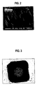
- FIG. 2 is an electron micrograph of a plurality of protrusions formed in an-GaN layer.
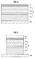
- FIG. 3 is an optical micrograph (a bright field image) of the semiconductor light emitting element taken from above.
- a semiconductor light emitting device (light emitting diode) 1 includes a supporting substrate 2, a p-side electrode 3, a reflection layer 4, a mask layer 5, a semiconductor stack 6, and an n-side electrode 7.
- the supporting substrate 2 is composed of a substrate with high heat radiation, such as a Cu substrate or an AIN substrate.
- the p-side electrode 3 is formed across an entire surface of the supporting substrate 2.
- the p-side electrode 3 is composed ofAu-Sn or Au.
- the reflection layer 4 includes an Au layer, a Pt layer, a Ti layer, and an Al layer sequentially stacked from the supporting substrate 2 side.
- the A1 layer may be replaced with another silver-gray metal layer such as an Ag layer.
- the reflection layer 4 is connected to a ZnO electrode 11 of the semiconductor stack 6 through a contact hole 5a formed in the mask layer 5.
- the mask layer 5 functions as an etching mask at etching of the semiconductor stack 6 in a later-described manufacturing step.
- the mask layer 5 is composed of a dielectric film of SiO 2 or the like or a resist film.
- the semiconductor stack 6 is supported on the supporting substrate 2 with the p-side electrode 3, reflection layer 4, and mask layer 5 interposed therebetween.
- the semiconductor stack 6 includes the ZnO electrode 11, a p-GaN layer 12, an MQW active layer 13, and an n-GaN layer 14.
- the ZnO electrode 11 has a low resistivity of about 2 ⁇ 10 -4 ⁇ cm and a thickness of about 1000 to 20000 ⁇ . Desirably, the thickness of the ZnO electrode 11 is about 8000 ⁇ .
- the p-GaN layer 12 is doped with Mg as a p-type dopant. Between the p-GaN layer 12 and MQW active layer 13, an undoped GaN layer or an InGaN layer containing about 1% In.
- the MQW active layer 13 includes eight In X Ga 1-X N well layers (not shown) about 30 ⁇ thick and eight undoped In Y Ga 1-Y N barrier layers (not shown) about 100 ⁇ thick alternately arranged on each other.
- an InGaN/GaN superlattice layer doped with Si (not shown) is formed.
- the n-GaN layer 14 is doped with Si as an n-type dopant.
- n-GaN layer 14 in the upper surface of the n-GaN layer 14, a plurality of conical (pyramid-shaped) protrusions 14a are formed.
- W A > ⁇ / n
- ⁇ wavelength of light emitted from the MQW active layer 13
- n the refractive index of the n-GaN layer 14.
- the refractive index of the n-GaN layer 14 is about 2.5, and therefore the above average W A is not less than about 184 nm.
- the above average W A is not less than about 146 nm.
- the image of the periphery where the conical protrusions 14a satisfying the above equation (1) are formed is black, and the periphery is therefore found to transmit light.
- the image of the center part where the protrusions satisfying the equation (1) are not formed is white, and the center part is therefore found to reflect light.
- the n-side electrode 7 is formed to cover a part of the n-GaN layer 14.
- the n-side electrode 7 includes Al/Ti/Au or AllMo/Au stacked from the n-GaN layer 14 side.
- the conical protrusions 14a satisfying the equation (1) are formed in the upper surface of the n-GaN layer 14 so as to easily transmit light emitted by the MQW active layer 13. Accordingly, most of the light emitted by the MQW active layer 13 is not reflected at the upper surface of the n-GaN layer 14 as an interface of the n-GaN layer 14 and air and emitted to the outside. This can increase the light extraction efficiency and therefore increase the brightness of the semiconductor light emitting device 1.
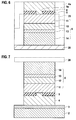
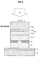
- FIGS. 4 to 8 are views each showing a cross sectional structure of the semiconductor light emitting device at each manufacturing step.
- a growth substrate 20 composed of a sapphire substrate side is conveyed to a growth chamber.
- the temperature inside the growth chamber is increased to about 1050°C while hydrogen gas continues to be supplied to the growth chamber for thermal cleaning of the growth substrate 20.
- the temperature of the growth chamber is reduced to about 600°C, and a GaN buffer layer (not shown) is grown on the growth substrate 20 using MOCVD.
- the temperature of the growth chamber is then increased to about 1000°C, and the n-GaN layer 14 doped with Si, the InGaN/GaN superlattice layer doped with Si, and the undoped GaN layer or InGaN layer containing about 1% In are sequentially stacked.
- the temperature of the growth chamber is then increased for growth of the p-GaN layer 12.
- annealing is performed to activate Mg in the p-type GaN layer 12.
- MBE molecular beam epitaxy
- the ZnO electrode 11 is formed (a stacking step).
- the mask layer 5 made of SiO 2 is formed.
- a resist film 21 is formed by photolithography.
- the mask layer 5 is then patterned by etching using the resist film 21 as a mask, and then the resist film 21 is removed.
- the ZnO electrode 11 to n-GaN layer 14 are mesa-etched up to the growth substrate 20 by inductively-coupled plasma (ICP) etching using the mask layer 5 as a mask.
- ICP inductively-coupled plasma
- the mesa-etching may be performed after the ZnO electrode 11 is patterned and the mask layer 5 made of SiO 2 is formed.
- the mask layer 5 is etched using dry etching with CF 4 to form the contact hole 5a to connect the reflection layer 4 and ZnO electrode 11.
- the ZnO electrode 11 is hardly etched by CF 4 and therefore serves as an etching stopper.
- a resist film 22 is formed, and Al or Au is deposited thereon. Thereafter, Ti/Pt/Au are sequentially layered.
- the metal layer 4a on the resist film 22 is removed together with the resist film 22 to form the reflection layer 4.
- the p-side electrode 3 of Au-Sn or Au is formed on the supporting substrate 2, and the semiconductor stack 6 is attached to the support substrate 2 by thermocompression bonding so that the p-side electrode 3 and reflection layer 4 are bonded to each other.
- a beam from a KrF laser oscillating at about 248 nm is projected from the growth substrate 20 side to the n-GaN layer 14.
- the beam of the KRF laser is substantially completely transmitted through the growth substrate 20 as the sapphire substrate and is substantially fully absorbed by the n-GaN layer 14.
- the temperature at the interface (the GaN buffer layer) between the growth substrate 20 and n-GaN layer 14 therefore rapidly increases to fuse the n-GaN layer 14 and GaN buffer layer near the interface.
- the growth substrate 20 can be thus lifted off (a laser lift off (LLO) process: a re-attachment step).
- LLO laser lift off
- energy of the KrF laser required to lift off the growth substrate 20 is about 300 to 700 mJ/cm 2 .
- N 2 generated when the n-GaN layer 14 is fused escapes to the adjacent semiconductor stack 6, and the semiconductor stack 6 is affected by pressure, thus preventing cracks of the semiconductor stack 6.
- unnecessary Ga droplets remaining on the upper surface of the n-GaN layer 14 are removed by etching with an acid, an alkali, or the like.
- a resist film (not shown) is formed, and a metal layer (not shown) composed of Al/Ti/Au or Al/Mo/Au is stacked. Thereafter, as shown in FIG. 8 , the metal layer is patterned using a lift off process to form the n-side electrode 7 allowing wire bonding on a part of the upper surface of the n-GaN layer 14.
- the upper surface of the n-GaN layer 14 with the growth substrate 20 removed is not composed of a Ga polar face but an N polar face tending to have anisotropy by etching.
- the n-GaN layer 14 is immersed in about 4 mol/l KOH solution at about 62°C and is exposed to ultra violet (UV) light of about 3.5 W/cm 2 for 10 minutes as shown in FIG. 8 , thus forming the plurality of conical protrusions whose average W A of the widths W of the bottom surfaces satisfies the equation (1) in the upper surface of the n-GaN layer 14 (photo enhanced chemical etching (PEC) (a surface roughening step)).
- PEC photo enhanced chemical etching
- the average of aspect ratios (height/bottom width) of the conical protrusions 14a formed in the above conditions is about 1.5.
- the aspect ratio is about 1.0.
- the conical shapes of the protrusions 14a can be therefore defined by changing the molar concentration of the KOH solution in such a manner.
- the semiconductor light emitting device 1 is thus completed.
- the protrusions 14a are formed into conical shapes in the above embodiment but may be formed into shapes each being elongated in any one direction and having a trapezoidal cross section.
- the above embodiment includes the plurality of protrusions 14a formed in the upper surface of the n-GaN layer 14 in the above embodiment but may include only a single protrusion formed in the n-GaN layer.
- the LLO process is performed using the KrF laser but may be performed using another exima laser (ArF: about 193 nm in wavelength, XeCl: about 308 nm in wavelength, YAG 3rd harmonic wave: about 355nm in wavelength, sapphire-titanium 3 rd harmonic wave: about 360 nm in wavelength, or He-Cd: about 325 nm in wavelength).
- ArF about 193 nm in wavelength
- XeCl about 308 nm in wavelength
- YAG 3rd harmonic wave about 355nm in wavelength
- sapphire-titanium 3 rd harmonic wave about 360 nm in wavelength
- He-Cd about 325 nm in wavelength
- the parameters in the manufacturing process of the semiconductor stack 6 can be properly changed.
Landscapes
- Led Devices (AREA)
- Weting (AREA)
Abstract
To provide a semiconductor light emitting device with a light extraction efficiency increased and a method for manufacturing the semiconductor light emitting device.
A semiconductor light emitting device 1 includes a supporting substrate 2 and a semiconductor stack 6 including an MQW active layer 13 emitting light and an n-GaN layer 14 at the top. In the upper surface of the n-GaN layer 14 of the semiconductor attack 6, a plurality of conical protrusions 14a are formed. The protrusions 14a are formed so that an average WA of widths W of bottom surfaces of protrusions 14 satisfies: WA>=λ/n, where λ is wavelength of light emitted from the active layer and n is a refractive index of the n-GaN layer 14.
Description
- The present invention relates to a semiconductor light emitting device having a plurality of protrusions at the top of a nitride system semiconductor stack and a method for manufacturing the semiconductor light emitting device.
- There have been known nitride system semiconductor light emitting devices containing GaN and the like. For example, white LEDs, each of which is a combination of a blue LED (light emitting diode) containing GaN and an yellow light emitter, are widely used as backlights of liquid crystal displays (LCDs) of mobile phones and the like. Moreover, the white LEDs are characterized by low power consumption and long lifetime. Accordingly, the white LEDs will be further expected as light sources alternative to fluorescent and incandescent lamps in the future and are being increasingly studied and developed.
- However, an LED outputs only about several watts and is therefore desired to increase in brightness. Conceivable means for increasing the brightness is increasing the internal quantum efficiency of the LED, increasing the extraction efficiency of extracting light emitted from an active layer to the outside, or the like. Since the light refractive index of GaN (about 2.5) is extremely higher than that of air (about 1.0) in particular, the total reflection angle at the interface between the LED and air is small, and the light extraction efficiency is very small (for example, about 10%).
- Accordingly, various techniques to increase the efficiency of extracting light emitted by a semiconductor light emitting device are disclosed.
- For example,
Patent Literature 1 discloses a semiconductor light emitting device including a semiconductor stack with the surface of the top layer roughened. - This semiconductor light emitting device includes a semiconductor stack having a p-GaN layer provided, an active layer, and an n-GaN layer on a substrate. The upper surface of the n-GaN layer formed in the top layer of the semiconductor stack has conical protrusions formed to be roughened. Roughening the upper surface of the n-GaN layer as described above can prevent light emitted by the active layer from being reflected at the interface between the n-GaN layer and air by Snell's law, thus increasing the amount of light emitted to the outside.
- In the method of manufacturing this semiconductor light emitting device, first, using MOCVD (metal organic chemical vapor deposition), the n-GaN layer, active layer, p-GaN layer are sequentially stacked on a growth substrate (a sapphire substrate) to form the semiconductor stack. Subsequently, a p-side electrode is formed on the p-GaN layer, and the semiconductor stack is then re-attached to a supporting substrate so that the p-side electrode is positioned on the supporting substrate (silicon substrate) side.
- Next, on the upper surface of the n-GaN layer at the top of the semiconductor stack reattached to the supporting substrate, an n-side electrode is formed. Thereafter, the upper surface of the n-GaN layer is formed into a rough surface with conical protrusions by PEC (photo-enhanced chemical) etching using KOH solution and a xenon/mercury lamp.
- International Publication Pamphlet No.
2005/064666 - However, depending on the refractive index of the n-GaN layer and wavelength of light emitted from the active layer, when the conical protrusions are small, the upper surface of the n-GaN layer acts on light in a same manner as a flat surface although the conical protrusions are formed. Accordingly, light is reflected on the upper surface of the n-GaN layer in the same manner as a flat surface, and the amount of reflected light is therefore increased. Accordingly, there is a problem of reduction in efficiency of extracting light to the outside.
- The present invention was invented to solve the aforementioned problem, and an object of the present invention is to provide a semiconductor light emitting device with a light extraction efficiency increased and a method of manufacturing the semiconductor light emitting device.
- To achieve the aforementioned object, an invention of
claim 1 is a semiconductor light emitting device including: a substrate; and a semiconductor stack which includes an active layer emitting light and is provided on the substrate, in which a single or a plurality of protrusions are formed in an upper surface of a semiconductor layer at a top of the semiconductor stack which emits light to the outside, and an average WA of widths of bottom surfaces of the protrusions satisfies WA>=λ/n, where λ is wavelength of light emitted from the active layer and n is a refractive index of the n-GaN layer of the semiconductor layer at the top. - An invention of
claim 2 is the semiconductor light emitting device ofclaim 1, in which the semiconductor layer at the top is an n-GaN layer. - An invention of
claim 3 is the semiconductor light emitting device ofclaim - An invention of
claim 4 is a method for manufacturing a semiconductor light emitting device including: a stacking step of forming a semiconductor stack including an active layer on a growth substrate; a re-attachment step of re-attaching the semiconductor stack to a supporting substrate; and a surface roughening step of immersing the semiconductor layer at a top of the semiconductor stack into a KOH (potassium hydroxide) solution while irradiating the semiconductor layer with UV (ultraviolet) light to form a single or a plurality of protrusions and thus roughen a surface of the semiconductor layer at the top. In the surface roughening step, the protrusions are formed to have an average WA of widths of bottom surfaces of the protrusions satisfying WA>=λ/n where λ is wavelength of light emitted from the active layer and n is a refractive index of the n-GaN layer of the semiconductor layer at the top. - An invention of
claim 5 is the method ofclaim 3, in which in the surface roughening step, shapes of the protrusions are determined based on a concentration of the KOH solution. - According to the present invention, by forming the protrusions satisfying the above equation on the upper surface of the semiconductor layer at the top so as to allow light emitted by the active layer to be easily transmitted through the semiconductor layer at the top, most of the light emitted by the active layer is not reflected on the upper surface of the semiconductor layer at the top, which is an interface between the semiconductor layer at the top and air, and can be emitted to the outside. This can increase the light extraction efficiency and thus increase the brightness of the semiconductor light emitting device.
-
-
FIG. 1 shows a cross-sectional structure of a semiconductor light emitting device according to the present invention. -
FIG. 2 is an electron micrograph of a plurality of protrusions formed in n-GaN layer. -
FIG. 3 is an optical micrograph (bright field image) of the semiconductor light emitting device taken from above. -
FIG. 4 is a view showing a cross-sectional structure of the semiconductor light emitting device in a manufacturing step according to a method for manufacturing a semiconductor light emitting device of the present invention. -
FIG. 5 is a view showing a cross-sectional structure of the semiconductor light emitting element in another manufacturing step according to the method of manufacturing a semiconductor light emitting device of the present invention. -
FIG. 6 is a view showing a cross-sectional structure of the semiconductor light emitting element in still another manufacturing step according to the method of manufacturing still another semiconductor light emitting device of the present invention. -
FIG. 7 is a view showing a cross-sectional structure of the semiconductor light emitting element in still another manufacturing step according to the method of manufacturing a semiconductor light emitting device of the present invention. -
FIG. 8 is a view showing a cross-sectional structure of the semiconductor light emitting element in a still another manufacturing step according to the method of manufacturing a semiconductor light emitting device of the present invention. -
- 1. SEMICONDUCTOR LIGHT EMITTING DEVICE
- 2. SUPPORTING SUBSTRATE
- 3. p-SIDE ELECTRODE
- 4. REFLECTION LAYER
- 4A. METAL LAYER
- 5. MASK LAYER
- 5A. CONTACT HOLE
- 6. SEMICONDUCTOR STACK
- 7. n-SIDE ELECTRODE
- 11. ZnO ELECTRODE
- 12. p-GaN LAYER
- 13. MQW ACTIVE LAYER
- 14. n-GaN LAYER
- 14A. PROTRUSION
- 20. GROWTH SUBSTRATE
- Hereinafter, a description is given of an embodiment of the present invention with reference to the drawings.
FIG. 1 shows a cross-sectional structure of a semiconductor light emitting device according to the present invention.FIG. 2 is an electron micrograph of a plurality of protrusions formed in an-GaN layer.FIG. 3 is an optical micrograph (a bright field image) of the semiconductor light emitting element taken from above. - As shown in
FIG. 1 , a semiconductor light emitting device (light emitting diode) 1 includes a supportingsubstrate 2, a p-side electrode 3, areflection layer 4, amask layer 5, asemiconductor stack 6, and an n-side electrode 7. - The supporting
substrate 2 is composed of a substrate with high heat radiation, such as a Cu substrate or an AIN substrate. The p-side electrode 3 is formed across an entire surface of the supportingsubstrate 2. The p-side electrode 3 is composed ofAu-Sn or Au. - The
reflection layer 4 includes an Au layer, a Pt layer, a Ti layer, and an Al layer sequentially stacked from the supportingsubstrate 2 side. The A1 layer may be replaced with another silver-gray metal layer such as an Ag layer. Thereflection layer 4 is connected to aZnO electrode 11 of thesemiconductor stack 6 through acontact hole 5a formed in themask layer 5. - The
mask layer 5 functions as an etching mask at etching of thesemiconductor stack 6 in a later-described manufacturing step. Themask layer 5 is composed of a dielectric film of SiO2 or the like or a resist film. - The
semiconductor stack 6 is supported on the supportingsubstrate 2 with the p-side electrode 3,reflection layer 4, andmask layer 5 interposed therebetween. Thesemiconductor stack 6 includes theZnO electrode 11, a p-GaN layer 12, an MQWactive layer 13, and an n-GaN layer 14. - The
ZnO electrode 11 has a low resistivity of about 2×10⁻⁴ Ω cm and a thickness of about 1000 to 20000 Å. Desirably, the thickness of theZnO electrode 11 is about 8000 Å. - The p-
GaN layer 12 is doped with Mg as a p-type dopant. Between the p-GaN layer 12 and MQWactive layer 13, an undoped GaN layer or an InGaN layer containing about 1% In. - The MQW
active layer 13 includes eight InXGa1-XN well layers (not shown) about 30 Å thick and eight undoped InYGa1-YN barrier layers (not shown) about 100 Å thick alternately arranged on each other. Herein, X and Y satisfy the following equations: 0<=X<=0.3 (desirably 0.1<=X<=0.2), 0<=Y<=0.1, and Y<=X. Between the MQWactive layer 13 and n-GaN layer 14, an InGaN/GaN superlattice layer doped with Si (not shown) is formed. The n-GaN layer 14 is doped with Si as an n-type dopant. - As shown in
FIGS. 1 and2 , in the upper surface of the n-GaN layer 14, a plurality of conical (pyramid-shaped)protrusions 14a are formed. Herein, an average WA of widths W of the bottom surfaces of theconical protrusions 14a satisfies:
where λ is wavelength of light emitted from the MQWactive layer 13 and n is the refractive index of the n-GaN layer 14. - For example, in the case of the blue semiconductor
light emitting device 1 having an InGaN layer emitting light with a peak wavelength of 460 nm as the well layer, the refractive index of the n-GaN layer 14 is about 2.5, and therefore the above average WA is not less than about 184 nm. In the case of the blue semiconductorlight emitting device 1 having a GaN layer emitting light with a peak wavelength of 365 nm as the well layer, the above average WA is not less than about 146 nm. - Herein, as apparent from the micrograph of
FIG. 3 , the image of the periphery where theconical protrusions 14a satisfying the above equation (1) are formed is black, and the periphery is therefore found to transmit light. On the other hand, the image of the center part where the protrusions satisfying the equation (1) are not formed is white, and the center part is therefore found to reflect light. - The n-
side electrode 7 is formed to cover a part of the n-GaN layer 14. The n-side electrode 7 includes Al/Ti/Au or AllMo/Au stacked from the n-GaN layer 14 side. - As described above, in the semiconductor
light emitting device 1 according to the present invention, theconical protrusions 14a satisfying the equation (1) are formed in the upper surface of the n-GaN layer 14 so as to easily transmit light emitted by the MQWactive layer 13. Accordingly, most of the light emitted by the MQWactive layer 13 is not reflected at the upper surface of the n-GaN layer 14 as an interface of the n-GaN layer 14 and air and emitted to the outside. This can increase the light extraction efficiency and therefore increase the brightness of the semiconductorlight emitting device 1. - Next, a description is given of a method for manufacturing the aforementioned semiconductor light emitting device with reference to the drawings.
FIGS. 4 to 8 are views each showing a cross sectional structure of the semiconductor light emitting device at each manufacturing step. - First, a
growth substrate 20 composed of a sapphire substrate side is conveyed to a growth chamber. Next, the temperature inside the growth chamber is increased to about 1050°C while hydrogen gas continues to be supplied to the growth chamber for thermal cleaning of thegrowth substrate 20. - Next, as shown in
FIG. 4 , the temperature of the growth chamber is reduced to about 600°C, and a GaN buffer layer (not shown) is grown on thegrowth substrate 20 using MOCVD. The temperature of the growth chamber is then increased to about 1000°C, and the n-GaN layer 14 doped with Si, the InGaN/GaN superlattice layer doped with Si, and the undoped GaN layer or InGaN layer containing about 1% In are sequentially stacked. - The temperature of the growth chamber is then increased for growth of the p-
GaN layer 12. Next, in order to convert the p-GaN layer 12 into p-type, annealing is performed to activate Mg in the p-type GaN layer 12. Next, using molecular beam epitaxy (MBE), theZnO electrode 11 is formed (a stacking step). Thereafter, themask layer 5 made of SiO2 is formed. - Next, as shown in
FIG. 5 , a resistfilm 21 is formed by photolithography. Themask layer 5 is then patterned by etching using the resistfilm 21 as a mask, and then the resistfilm 21 is removed. - Next, the
ZnO electrode 11 to n-GaN layer 14 are mesa-etched up to thegrowth substrate 20 by inductively-coupled plasma (ICP) etching using themask layer 5 as a mask. The mesa-etching may be performed after theZnO electrode 11 is patterned and themask layer 5 made of SiO2 is formed. - Next, as shown in
FIG. 6 , themask layer 5 is etched using dry etching with CF4 to form thecontact hole 5a to connect thereflection layer 4 andZnO electrode 11. - Herein, the
ZnO electrode 11 is hardly etched by CF4 and therefore serves as an etching stopper. Next, a resistfilm 22 is formed, and Al or Au is deposited thereon. Thereafter, Ti/Pt/Au are sequentially layered. Next, themetal layer 4a on the resistfilm 22 is removed together with the resistfilm 22 to form thereflection layer 4. - Next, as shown in
FIG. 7 , the p-side electrode 3 of Au-Sn or Au is formed on the supportingsubstrate 2, and thesemiconductor stack 6 is attached to thesupport substrate 2 by thermocompression bonding so that the p-side electrode 3 andreflection layer 4 are bonded to each other. - Thereafter, a beam from a KrF laser oscillating at about 248 nm is projected from the
growth substrate 20 side to the n-GaN layer 14. The beam of the KRF laser is substantially completely transmitted through thegrowth substrate 20 as the sapphire substrate and is substantially fully absorbed by the n-GaN layer 14. The temperature at the interface (the GaN buffer layer) between thegrowth substrate 20 and n-GaN layer 14 therefore rapidly increases to fuse the n-GaN layer 14 and GaN buffer layer near the interface. Thegrowth substrate 20 can be thus lifted off (a laser lift off (LLO) process: a re-attachment step). - Herein, energy of the KrF laser required to lift off the
growth substrate 20 is about 300 to 700 mJ/cm2. N2 generated when the n-GaN layer 14 is fused escapes to theadjacent semiconductor stack 6, and thesemiconductor stack 6 is affected by pressure, thus preventing cracks of thesemiconductor stack 6. After thegrowth substrate 20 is separated, unnecessary Ga droplets remaining on the upper surface of the n-GaN layer 14 are removed by etching with an acid, an alkali, or the like. - Next, a resist film (not shown) is formed, and a metal layer (not shown) composed of Al/Ti/Au or Al/Mo/Au is stacked. Thereafter, as shown in
FIG. 8 , the metal layer is patterned using a lift off process to form the n-side electrode 7 allowing wire bonding on a part of the upper surface of the n-GaN layer 14. - Herein, the upper surface of the n-
GaN layer 14 with thegrowth substrate 20 removed is not composed of a Ga polar face but an N polar face tending to have anisotropy by etching. In this state, the n-GaN layer 14 is immersed in about 4 mol/l KOH solution at about 62°C and is exposed to ultra violet (UV) light of about 3.5 W/cm2 for 10 minutes as shown inFIG. 8 , thus forming the plurality of conical protrusions whose average WA of the widths W of the bottom surfaces satisfies the equation (1) in the upper surface of the n-GaN layer 14 (photo enhanced chemical etching (PEC) (a surface roughening step)). - The average of aspect ratios (height/bottom width) of the
conical protrusions 14a formed in the above conditions is about 1.5. Herein, when the molar concentration of the KOH solution is about 2.0 mol/l, the aspect ratio is about 1.0. The conical shapes of theprotrusions 14a can be therefore defined by changing the molar concentration of the KOH solution in such a manner. - The semiconductor
light emitting device 1 is thus completed. - Hereinabove, the present invention is described using the embodiment, but it is apparent to those skilled in the art that the present invention is not limited to the embodiment described in the specification. The present invention can be carried out as modified and changed modes without departing from the spirit and scope of the invention defined by the description of claims. Accordingly, the description of this specification is for illustrative purposes and does not impose any limitation on the present invention. A description is given below of modified modes obtained by partially changing the embodiment.
- For example, the
protrusions 14a are formed into conical shapes in the above embodiment but may be formed into shapes each being elongated in any one direction and having a trapezoidal cross section. - Moreover, the above embodiment includes the plurality of
protrusions 14a formed in the upper surface of the n-GaN layer 14 in the above embodiment but may include only a single protrusion formed in the n-GaN layer. - In the above embodiment, the LLO process is performed using the KrF laser but may be performed using another exima laser (ArF: about 193 nm in wavelength, XeCl: about 308 nm in wavelength, YAG 3rd harmonic wave: about 355nm in wavelength, sapphire-
titanium 3rd harmonic wave: about 360 nm in wavelength, or He-Cd: about 325 nm in wavelength). - Materials and the like constituting the
semiconductor stack 6 and bothelectrodes - The parameters in the manufacturing process of the
semiconductor stack 6 can be properly changed.
Claims (5)
- A semiconductor light emitting device, comprising:a substrate; anda semiconductor stack which includes an active layer emitting light and is provided on the substrate,wherein a single or a plurality of protrusions are formed in an upper surface of a semiconductor layer at a top of the semiconductor stack which emits light to the outside, andan average WA of widths of bottom surfaces of the protrusions satisfies WA>=λ/n, where λ is wavelength of light emitted from the active layer and n is a refractive index of the n-GaN layer of the semiconductor layer at the top.
- The device of claim 1, wherein
the semiconductor layer at the top is an n-GaN layer. - The device of claim 1 or 2, wherein
the protrusions are conical shaped. - A method for manufacturing a semiconductor light emitting device comprising:a stacking step of forming a semiconductor stack including an active layer on a growth substrate;a re-attachment step of re-attaching the semiconductor stack to a supporting substrate; anda surface roughening step of immersing the semiconductor layer at a top of the semiconductor stack into a KOH (potassium hydroxide) solution while irradiating the semiconductor layer with UV (ultraviolet) light to form a single or a plurality of protrusions and thus roughen a surface of the semiconductor layer at the top,wherein in the surface roughening step, the protrusions are formed to have an average WA of widths of bottom surfaces of the protrusions satisfying WA>=λ/n where λ is wavelength of light emitted from the active layer and n is a refractive index of the n-GaN layer of the semiconductor layer at the top layer.
- The method of claim 4, wherein
in the surface roughening step, shapes of the protrusions are determined based on a concentration of the KOH solution.
Applications Claiming Priority (2)
| Application Number | Priority Date | Filing Date | Title |
|---|---|---|---|
| JP2005356800A JP2007165409A (en) | 2005-12-09 | 2005-12-09 | Semiconductor light emitting device and method for manufacturing semiconductor light emitting device |
| PCT/JP2006/324436 WO2007066716A1 (en) | 2005-12-09 | 2006-12-07 | Semiconductor light emitting element and method for manufacturing semiconductor light emitting element |
Publications (2)
| Publication Number | Publication Date |
|---|---|
| EP1959503A1 true EP1959503A1 (en) | 2008-08-20 |
| EP1959503A4 EP1959503A4 (en) | 2011-01-05 |
Family
ID=38122861
Family Applications (1)
| Application Number | Title | Priority Date | Filing Date |
|---|---|---|---|
| EP06834191A Withdrawn EP1959503A4 (en) | 2005-12-09 | 2006-12-07 | SEMICONDUCTOR ELECTROLUMINESCENT ELEMENT AND METHOD FOR MANUFACTURING THE SAME |
Country Status (7)
| Country | Link |
|---|---|
| US (1) | US8198645B2 (en) |
| EP (1) | EP1959503A4 (en) |
| JP (1) | JP2007165409A (en) |
| KR (1) | KR20080073317A (en) |
| CN (1) | CN101322255B (en) |
| TW (1) | TW200739946A (en) |
| WO (1) | WO2007066716A1 (en) |
Cited By (3)
| Publication number | Priority date | Publication date | Assignee | Title |
|---|---|---|---|---|
| US8395173B2 (en) | 2008-10-29 | 2013-03-12 | Panasonic Corporation | Semiconductor light-emitting element, method of manufacturing same, and light-emitting device |
| EP2525420A3 (en) * | 2011-05-16 | 2013-09-04 | Kabushiki Kaisha Toshiba | Semiconductor light emitting device |
| EP2372790A3 (en) * | 2010-04-05 | 2014-07-02 | LG Innotek Co., Ltd | Light emitting diode, light emitting diode package, and lighting system |
Families Citing this family (36)
| Publication number | Priority date | Publication date | Assignee | Title |
|---|---|---|---|---|
| JP2007300069A (en) * | 2006-04-04 | 2007-11-15 | Toyoda Gosei Co Ltd | LIGHT EMITTING ELEMENT, LIGHT EMITTING DEVICE USING THE LIGHT EMITTING ELEMENT, AND METHOD FOR PRODUCING THE LIGHT EMITTING ELEMENT |
| JP2009049371A (en) * | 2007-07-26 | 2009-03-05 | Sharp Corp | Nitride-based compound semiconductor light-emitting device and method for manufacturing the same |
| JP4829190B2 (en) * | 2007-08-22 | 2011-12-07 | 株式会社東芝 | Light emitting element |
| DE102007046519A1 (en) * | 2007-09-28 | 2009-04-02 | Osram Opto Semiconductors Gmbh | Thin-film LED with a mirror layer and method for its production |
| KR20100097179A (en) | 2007-11-30 | 2010-09-02 | 더 리전트 오브 더 유니버시티 오브 캘리포니아 | High light extraction efficiency nitride based light emitting diode by surface roughening |
| RU2436195C1 (en) * | 2007-12-28 | 2011-12-10 | Нития Корпорейшн | Semiconductor light-emitting instrument and method for its manufacturing |
| JP5234454B2 (en) * | 2008-03-26 | 2013-07-10 | スタンレー電気株式会社 | Method for manufacturing optical semiconductor element |
| KR101534848B1 (en) | 2008-07-21 | 2015-07-27 | 엘지이노텍 주식회사 | Light emitting diode and method for fabricating the light emitting diode, and light emitting device and method for fabricating light emitting devcie |
| US8754425B2 (en) * | 2008-09-08 | 2014-06-17 | 3M Innovative Properties Company | Electrically pixelated luminescent device |
| WO2010036602A1 (en) * | 2008-09-26 | 2010-04-01 | S.O.I.Tec Silicon On Insulator Technologies | Method of forming a composite laser substrate |
| JP5226449B2 (en) * | 2008-10-03 | 2013-07-03 | スタンレー電気株式会社 | Semiconductor light emitting device |
| KR101018179B1 (en) * | 2008-10-16 | 2011-02-28 | 삼성엘이디 주식회사 | Pattern formation method of group III nitride semiconductor substrate and manufacturing method of group III nitride semiconductor light emitting device |
| JP5191866B2 (en) * | 2008-11-12 | 2013-05-08 | スタンレー電気株式会社 | Semiconductor light emitting device manufacturing method and semiconductor light emitting device |
| EP2356701A2 (en) * | 2008-11-13 | 2011-08-17 | 3M Innovative Properties Company | Electrically pixelated luminescent device incorporating optical elements |
| KR101363022B1 (en) * | 2008-12-23 | 2014-02-14 | 삼성디스플레이 주식회사 | Organic light emitting diode display |
| KR100992743B1 (en) * | 2008-12-26 | 2010-11-05 | 엘지이노텍 주식회사 | Light emitting device and manufacturing method |
| KR100969160B1 (en) * | 2009-03-10 | 2010-07-21 | 엘지이노텍 주식회사 | Light emitting device and method for fabricating the same |
| KR101662037B1 (en) * | 2009-12-02 | 2016-10-05 | 삼성전자 주식회사 | Light Emitting Device and method for manufacturing the same |
| KR100986560B1 (en) * | 2010-02-11 | 2010-10-07 | 엘지이노텍 주식회사 | Light emitting device and fabrication method thereof |
| JP4996706B2 (en) | 2010-03-03 | 2012-08-08 | 株式会社東芝 | Semiconductor light emitting device and manufacturing method thereof |
| KR101047720B1 (en) * | 2010-04-23 | 2011-07-08 | 엘지이노텍 주식회사 | Light emitting device, method of manufacturing light emitting device, |
| KR101182920B1 (en) * | 2010-07-05 | 2012-09-13 | 엘지이노텍 주식회사 | Light emitting device and fabrication method thereof |
| JP2012033537A (en) * | 2010-07-28 | 2012-02-16 | Toshiba Corp | Light-emitting element |
| TW201216503A (en) * | 2010-10-12 | 2012-04-16 | Tekcore Co Ltd | Method for fabricating a vertical light-emitting diode with high brightness |
| JP5589812B2 (en) * | 2010-12-06 | 2014-09-17 | 豊田合成株式会社 | Semiconductor light emitting device |
| KR101233768B1 (en) * | 2010-12-30 | 2013-02-15 | 포항공과대학교 산학협력단 | Nano imprint mold manufacturing method, light emitting diode manufacturing method and light emitting diode using the nano imprint mold manufactured by the method |
| US9012921B2 (en) | 2011-09-29 | 2015-04-21 | Kabushiki Kaisha Toshiba | Light emitting devices having light coupling layers |
| JP5912442B2 (en) * | 2011-11-17 | 2016-04-27 | スタンレー電気株式会社 | Semiconductor light emitting device and method for manufacturing semiconductor light emitting device |
| KR101286211B1 (en) * | 2012-02-16 | 2013-07-15 | 고려대학교 산학협력단 | Method of fabricating light emitting device and light emitting device fabricated by using the same |
| JP2015524167A (en) * | 2012-06-01 | 2015-08-20 | コーニンクレッカ フィリップス エヌ ヴェ | Improved light extraction using feature size and shape control in roughing LED surfaces |
| US20140167059A1 (en) * | 2012-08-30 | 2014-06-19 | The Regents Of The University Of California | Pec etching of (20-2-1) semipolar gallium nitride for external efficiency enhancement in light emitting diode applications |
| US9048363B2 (en) | 2013-05-20 | 2015-06-02 | International Business Machines Corporation | Elemental semiconductor material contact for high indium content InGaN light emitting diodes |
| US8933434B2 (en) | 2013-05-20 | 2015-01-13 | International Business Machines Company | Elemental semiconductor material contact for GaN-based light emitting diodes |
| US8877525B1 (en) | 2013-07-25 | 2014-11-04 | International Business Machines Corporation | Low cost secure chip identification |
| TWI565098B (en) * | 2015-06-10 | 2017-01-01 | 隆達電子股份有限公司 | Light emitting device |
| KR102659984B1 (en) * | 2019-06-21 | 2024-04-24 | 엘지전자 주식회사 | Display device using micro led and manufacturing method thereof |
Family Cites Families (44)
| Publication number | Priority date | Publication date | Assignee | Title |
|---|---|---|---|---|
| JPH0442582A (en) * | 1990-06-08 | 1992-02-13 | Eastman Kodak Japan Kk | light emitting diode array |
| JP2836687B2 (en) * | 1993-04-03 | 1998-12-14 | 日亜化学工業株式会社 | Gallium nitride based compound semiconductor light emitting device |
| US5751752A (en) * | 1994-09-14 | 1998-05-12 | Rohm Co., Ltd. | Semiconductor light emitting device and manufacturing method therefor |
| JPH0888439A (en) * | 1994-09-16 | 1996-04-02 | Rohm Co Ltd | Semiconductor laser and its production |
| US5889295A (en) * | 1996-02-26 | 1999-03-30 | Kabushiki Kaisha Toshiba | Semiconductor device |
| US5779924A (en) * | 1996-03-22 | 1998-07-14 | Hewlett-Packard Company | Ordered interface texturing for a light emitting device |
| JP3448441B2 (en) * | 1996-11-29 | 2003-09-22 | 三洋電機株式会社 | Light emitting device |
| US6015979A (en) * | 1997-08-29 | 2000-01-18 | Kabushiki Kaisha Toshiba | Nitride-based semiconductor element and method for manufacturing the same |
| US6171164B1 (en) * | 1998-02-19 | 2001-01-09 | Micron Technology, Inc. | Method for forming uniform sharp tips for use in a field emission array |
| JP2000022128A (en) * | 1998-07-06 | 2000-01-21 | Murata Mfg Co Ltd | Semiconductor light emitting device and optoelectronic integrated circuit device |
| US6504180B1 (en) * | 1998-07-28 | 2003-01-07 | Imec Vzw And Vrije Universiteit | Method of manufacturing surface textured high-efficiency radiating devices and devices obtained therefrom |
| JP3289682B2 (en) * | 1998-08-17 | 2002-06-10 | 株式会社村田製作所 | Semiconductor light emitting device |
| JP3584748B2 (en) * | 1998-09-10 | 2004-11-04 | 富士電機ホールディングス株式会社 | Fluorescence conversion filter and color display device having the filter |
| WO2000016455A1 (en) * | 1998-09-10 | 2000-03-23 | Rohm Co., Ltd. | Semiconductor luminous element and semiconductor laser |
| US20010042866A1 (en) * | 1999-02-05 | 2001-11-22 | Carrie Carter Coman | Inxalygazn optical emitters fabricated via substrate removal |
| JP3594826B2 (en) * | 1999-02-09 | 2004-12-02 | パイオニア株式会社 | Nitride semiconductor light emitting device and method of manufacturing the same |
| JP3786544B2 (en) * | 1999-06-10 | 2006-06-14 | パイオニア株式会社 | Nitride semiconductor device manufacturing method and device manufactured by the method |
| JP2001177145A (en) * | 1999-12-21 | 2001-06-29 | Toshiba Electronic Engineering Corp | Semiconductor light emitting device and method of manufacturing the same |
| US6535536B2 (en) * | 2000-04-10 | 2003-03-18 | Fuji Photo Film Co., Ltd. | Semiconductor laser element |
| US6836498B2 (en) * | 2000-06-05 | 2004-12-28 | Sony Corporation | Semiconductor laser, semiconductor device and nitride series III-V group compound substrate, as well as manufacturing method thereof |
| TW472400B (en) * | 2000-06-23 | 2002-01-11 | United Epitaxy Co Ltd | Method for roughing semiconductor device surface to increase the external quantum efficiency |
| US6608360B2 (en) * | 2000-12-15 | 2003-08-19 | University Of Houston | One-chip micro-integrated optoelectronic sensor |
| US6946788B2 (en) * | 2001-05-29 | 2005-09-20 | Toyoda Gosei Co., Ltd. | Light-emitting element |
| TW564584B (en) * | 2001-06-25 | 2003-12-01 | Toshiba Corp | Semiconductor light emitting device |
| TW576864B (en) * | 2001-12-28 | 2004-02-21 | Toshiba Corp | Method for manufacturing a light-emitting device |
| JP3802424B2 (en) * | 2002-01-15 | 2006-07-26 | 株式会社東芝 | Semiconductor light emitting device and manufacturing method thereof |
| JP3782357B2 (en) * | 2002-01-18 | 2006-06-07 | 株式会社東芝 | Manufacturing method of semiconductor light emitting device |
| JP4122785B2 (en) * | 2002-01-30 | 2008-07-23 | 日亜化学工業株式会社 | Light emitting element |
| JP4233268B2 (en) * | 2002-04-23 | 2009-03-04 | シャープ株式会社 | Nitride-based semiconductor light-emitting device and manufacturing method thereof |
| US7002182B2 (en) * | 2002-09-06 | 2006-02-21 | Sony Corporation | Semiconductor light emitting device integral type semiconductor light emitting unit image display unit and illuminating unit |
| US6855571B1 (en) * | 2003-02-14 | 2005-02-15 | Matsushita Electric Industrial Co., Ltd. | Method of producing GaN-based semiconductor laser device and semiconductor substrate used therefor |
| US7078735B2 (en) * | 2003-03-27 | 2006-07-18 | Sanyo Electric Co., Ltd. | Light-emitting device and illuminator |
| TWI234298B (en) * | 2003-11-18 | 2005-06-11 | Itswell Co Ltd | Semiconductor light emitting diode and method for manufacturing the same |
| US7704763B2 (en) * | 2003-12-09 | 2010-04-27 | The Regents Of The University Of California | Highly efficient group-III nitride based light emitting diodes via fabrication of structures on an N-face surface |
| JP2005197608A (en) * | 2004-01-09 | 2005-07-21 | Mitsubishi Heavy Ind Ltd | Photoelectric converting device |
| TWI244221B (en) * | 2004-03-01 | 2005-11-21 | Epistar Corp | Micro-reflector containing flip-chip light emitting device |
| US20050236630A1 (en) * | 2004-04-23 | 2005-10-27 | Wang-Nang Wang | Transparent contact for light emitting diode |
| US7279751B2 (en) * | 2004-06-21 | 2007-10-09 | Matsushita Electric Industrial Co., Ltd. | Semiconductor laser device and manufacturing method thereof |
| CN1820378A (en) * | 2004-07-12 | 2006-08-16 | 罗姆股份有限公司 | Semiconductor light-emitting device |
| US7442964B2 (en) * | 2004-08-04 | 2008-10-28 | Philips Lumileds Lighting Company, Llc | Photonic crystal light emitting device with multiple lattices |
| US7476910B2 (en) * | 2004-09-10 | 2009-01-13 | Kabushiki Kaisha Toshiba | Semiconductor light emitting device and method for manufacturing the same |
| KR100664986B1 (en) * | 2004-10-29 | 2007-01-09 | 삼성전기주식회사 | Nitride-based semiconductor device using nanorods and manufacturing method thereof |
| JP4670489B2 (en) * | 2005-06-06 | 2011-04-13 | 日立電線株式会社 | Light emitting diode and manufacturing method thereof |
| US20070029541A1 (en) * | 2005-08-04 | 2007-02-08 | Huoping Xin | High efficiency light emitting device |
-
2005
- 2005-12-09 JP JP2005356800A patent/JP2007165409A/en active Pending
-
2006
- 2006-12-07 EP EP06834191A patent/EP1959503A4/en not_active Withdrawn
- 2006-12-07 CN CN2006800454756A patent/CN101322255B/en not_active Expired - Fee Related
- 2006-12-07 US US12/086,177 patent/US8198645B2/en not_active Expired - Fee Related
- 2006-12-07 KR KR1020087013421A patent/KR20080073317A/en not_active Ceased
- 2006-12-07 TW TW095145707A patent/TW200739946A/en unknown
- 2006-12-07 WO PCT/JP2006/324436 patent/WO2007066716A1/en not_active Ceased
Cited By (7)
| Publication number | Priority date | Publication date | Assignee | Title |
|---|---|---|---|---|
| US8395173B2 (en) | 2008-10-29 | 2013-03-12 | Panasonic Corporation | Semiconductor light-emitting element, method of manufacturing same, and light-emitting device |
| EP2372790A3 (en) * | 2010-04-05 | 2014-07-02 | LG Innotek Co., Ltd | Light emitting diode, light emitting diode package, and lighting system |
| EP2525420A3 (en) * | 2011-05-16 | 2013-09-04 | Kabushiki Kaisha Toshiba | Semiconductor light emitting device |
| EP2879193A1 (en) * | 2011-05-16 | 2015-06-03 | Kabushiki Kaisha Toshiba | Semiconductor light emitting device |
| US9082931B2 (en) | 2011-05-16 | 2015-07-14 | Kabushiki Kaisha Toshiba | Semiconductor light emitting device |
| US9299889B2 (en) | 2011-05-16 | 2016-03-29 | Kabushiki Kaisha Toshiba | Semiconductor light emitting device |
| US9368682B2 (en) | 2011-05-16 | 2016-06-14 | Kabushiki Kaisha Toshiba | Semiconductor light emitting device |
Also Published As
| Publication number | Publication date |
|---|---|
| WO2007066716A1 (en) | 2007-06-14 |
| US20090278145A1 (en) | 2009-11-12 |
| US8198645B2 (en) | 2012-06-12 |
| CN101322255A (en) | 2008-12-10 |
| CN101322255B (en) | 2012-09-05 |
| KR20080073317A (en) | 2008-08-08 |
| JP2007165409A (en) | 2007-06-28 |
| TW200739946A (en) | 2007-10-16 |
| EP1959503A4 (en) | 2011-01-05 |
Similar Documents
| Publication | Publication Date | Title |
|---|---|---|
| US8198645B2 (en) | Semiconductor light emitting device and method for manufacturing the same | |
| US9224917B2 (en) | Light emitting diode having photonic crystal structure and method of fabricating the same | |
| US8012779B2 (en) | Gallium nitride-based light emitting diode and method of manufacturing the same | |
| CN101026213B (en) | Light emitting device and method of manufacturing the same | |
| KR101125395B1 (en) | Light emitting device and fabrication method thereof | |
| TWI408832B (en) | Light-emitting element having a columnar structure having a hollow structure and method of forming the same | |
| JP2008277651A (en) | Light emitting diode | |
| CN101375419A (en) | Nitride semiconductor light emitting element | |
| JP2013251496A (en) | Light emitting element and method for manufacturing the same | |
| CN100416876C (en) | Semiconductor light emitting device | |
| US7521329B2 (en) | Semiconductor light emitting diode having textured structure and method of manufacturing the same | |
| JP5165668B2 (en) | Semiconductor light emitting device and manufacturing method thereof | |
| JP2008140918A (en) | Method for manufacturing light emitting device | |
| US20050079642A1 (en) | Manufacturing method of nitride semiconductor device | |
| JP2009123836A (en) | Nitride semiconductor light-emitting element | |
| JP2007200932A (en) | Manufacturing method of nitride semiconductor element | |
| CN108604623B (en) | Conversion element and radiation-emitting semiconductor component having such a conversion element | |
| TW201417333A (en) | Illuminating device comprising a shaped substrate | |
| JP2005142532A (en) | Method of manufacturing nitride semiconductor device | |
| US20230238485A1 (en) | Light emitting device and method of manufacturing the same | |
| TW202412339A (en) | Metallic layer for dimming light-emitting diode chips | |
| JP2007273590A (en) | Nitride semiconductor element and its manufacturing method | |
| KR100781660B1 (en) | Light emitting device having light emitting band and manufacturing method thereof | |
| KR102260691B1 (en) | Light-emitting diodes and method of manufacturing the same | |
| KR20090041179A (en) | Light emitting diodes and manufacturing method thereof |
Legal Events
| Date | Code | Title | Description |
|---|---|---|---|
| PUAI | Public reference made under article 153(3) epc to a published international application that has entered the european phase |
Free format text: ORIGINAL CODE: 0009012 |
|
| 17P | Request for examination filed |
Effective date: 20080610 |
|
| AK | Designated contracting states |
Kind code of ref document: A1 Designated state(s): DE GB |
|
| RIN1 | Information on inventor provided before grant (corrected) |
Inventor name: SAKAI, MITSUHIKO,C/O ROHM CO., LTD. |
|
| DAX | Request for extension of the european patent (deleted) | ||
| RBV | Designated contracting states (corrected) |
Designated state(s): DE GB |
|
| A4 | Supplementary search report drawn up and despatched |
Effective date: 20101207 |
|
| STAA | Information on the status of an ep patent application or granted ep patent |
Free format text: STATUS: THE APPLICATION IS DEEMED TO BE WITHDRAWN |
|
| 18D | Application deemed to be withdrawn |
Effective date: 20130702 |