EP1959495A1 - Trench gate power semiconductor device - Google Patents
Trench gate power semiconductor device Download PDFInfo
- Publication number
- EP1959495A1 EP1959495A1 EP05809501A EP05809501A EP1959495A1 EP 1959495 A1 EP1959495 A1 EP 1959495A1 EP 05809501 A EP05809501 A EP 05809501A EP 05809501 A EP05809501 A EP 05809501A EP 1959495 A1 EP1959495 A1 EP 1959495A1
- Authority
- EP
- European Patent Office
- Prior art keywords
- trench
- region
- conductive type
- gate power
- trenches
- Prior art date
- Legal status (The legal status is an assumption and is not a legal conclusion. Google has not performed a legal analysis and makes no representation as to the accuracy of the status listed.)
- Granted
Links
Images





Classifications
-
- H—ELECTRICITY
- H10—SEMICONDUCTOR DEVICES; ELECTRIC SOLID-STATE DEVICES NOT OTHERWISE PROVIDED FOR
- H10D—INORGANIC ELECTRIC SEMICONDUCTOR DEVICES
- H10D30/00—Field-effect transistors [FET]
- H10D30/60—Insulated-gate field-effect transistors [IGFET]
- H10D30/64—Double-diffused metal-oxide semiconductor [DMOS] FETs
- H10D30/66—Vertical DMOS [VDMOS] FETs
- H10D30/668—Vertical DMOS [VDMOS] FETs having trench gate electrodes, e.g. UMOS transistors
-
- H—ELECTRICITY
- H10—SEMICONDUCTOR DEVICES; ELECTRIC SOLID-STATE DEVICES NOT OTHERWISE PROVIDED FOR
- H10D—INORGANIC ELECTRIC SEMICONDUCTOR DEVICES
- H10D12/00—Bipolar devices controlled by the field effect, e.g. insulated-gate bipolar transistors [IGBT]
- H10D12/01—Manufacture or treatment
- H10D12/031—Manufacture or treatment of IGBTs
- H10D12/032—Manufacture or treatment of IGBTs of vertical IGBTs
- H10D12/038—Manufacture or treatment of IGBTs of vertical IGBTs having a recessed gate, e.g. trench-gate IGBTs
-
- H—ELECTRICITY
- H10—SEMICONDUCTOR DEVICES; ELECTRIC SOLID-STATE DEVICES NOT OTHERWISE PROVIDED FOR
- H10D—INORGANIC ELECTRIC SEMICONDUCTOR DEVICES
- H10D12/00—Bipolar devices controlled by the field effect, e.g. insulated-gate bipolar transistors [IGBT]
- H10D12/411—Insulated-gate bipolar transistors [IGBT]
- H10D12/441—Vertical IGBTs
- H10D12/461—Vertical IGBTs having non-planar surfaces, e.g. having trenches, recesses or pillars in the surfaces of the emitter, base or collector regions
- H10D12/481—Vertical IGBTs having non-planar surfaces, e.g. having trenches, recesses or pillars in the surfaces of the emitter, base or collector regions having gate structures on slanted surfaces, on vertical surfaces, or in grooves, e.g. trench gate IGBTs
-
- H—ELECTRICITY
- H10—SEMICONDUCTOR DEVICES; ELECTRIC SOLID-STATE DEVICES NOT OTHERWISE PROVIDED FOR
- H10D—INORGANIC ELECTRIC SEMICONDUCTOR DEVICES
- H10D30/00—Field-effect transistors [FET]
- H10D30/01—Manufacture or treatment
- H10D30/021—Manufacture or treatment of FETs having insulated gates [IGFET]
- H10D30/028—Manufacture or treatment of FETs having insulated gates [IGFET] of double-diffused metal oxide semiconductor [DMOS] FETs
- H10D30/0291—Manufacture or treatment of FETs having insulated gates [IGFET] of double-diffused metal oxide semiconductor [DMOS] FETs of vertical DMOS [VDMOS] FETs
- H10D30/0295—Manufacture or treatment of FETs having insulated gates [IGFET] of double-diffused metal oxide semiconductor [DMOS] FETs of vertical DMOS [VDMOS] FETs using recessing of the source electrodes
-
- H—ELECTRICITY
- H10—SEMICONDUCTOR DEVICES; ELECTRIC SOLID-STATE DEVICES NOT OTHERWISE PROVIDED FOR
- H10D—INORGANIC ELECTRIC SEMICONDUCTOR DEVICES
- H10D30/00—Field-effect transistors [FET]
- H10D30/01—Manufacture or treatment
- H10D30/021—Manufacture or treatment of FETs having insulated gates [IGFET]
- H10D30/028—Manufacture or treatment of FETs having insulated gates [IGFET] of double-diffused metal oxide semiconductor [DMOS] FETs
- H10D30/0291—Manufacture or treatment of FETs having insulated gates [IGFET] of double-diffused metal oxide semiconductor [DMOS] FETs of vertical DMOS [VDMOS] FETs
- H10D30/0297—Manufacture or treatment of FETs having insulated gates [IGFET] of double-diffused metal oxide semiconductor [DMOS] FETs of vertical DMOS [VDMOS] FETs using recessing of the gate electrodes, e.g. to form trench gate electrodes
-
- H—ELECTRICITY
- H10—SEMICONDUCTOR DEVICES; ELECTRIC SOLID-STATE DEVICES NOT OTHERWISE PROVIDED FOR
- H10D—INORGANIC ELECTRIC SEMICONDUCTOR DEVICES
- H10D30/00—Field-effect transistors [FET]
- H10D30/60—Insulated-gate field-effect transistors [IGFET]
- H10D30/64—Double-diffused metal-oxide semiconductor [DMOS] FETs
- H10D30/66—Vertical DMOS [VDMOS] FETs
- H10D30/665—Vertical DMOS [VDMOS] FETs having edge termination structures
-
- H—ELECTRICITY
- H10—SEMICONDUCTOR DEVICES; ELECTRIC SOLID-STATE DEVICES NOT OTHERWISE PROVIDED FOR
- H10D—INORGANIC ELECTRIC SEMICONDUCTOR DEVICES
- H10D62/00—Semiconductor bodies, or regions thereof, of devices having potential barriers
- H10D62/10—Shapes, relative sizes or dispositions of the regions of the semiconductor bodies; Shapes of the semiconductor bodies
- H10D62/17—Semiconductor regions connected to electrodes not carrying current to be rectified, amplified or switched, e.g. channel regions
- H10D62/393—Body regions of DMOS transistors or IGBTs
-
- H—ELECTRICITY
- H10—SEMICONDUCTOR DEVICES; ELECTRIC SOLID-STATE DEVICES NOT OTHERWISE PROVIDED FOR
- H10D—INORGANIC ELECTRIC SEMICONDUCTOR DEVICES
- H10D84/00—Integrated devices formed in or on semiconductor substrates that comprise only semiconducting layers, e.g. on Si wafers or on GaAs-on-Si wafers
- H10D84/101—Integrated devices comprising main components and built-in components, e.g. IGBT having built-in freewheel diode
- H10D84/141—VDMOS having built-in components
- H10D84/143—VDMOS having built-in components the built-in components being PN junction diodes
- H10D84/144—VDMOS having built-in components the built-in components being PN junction diodes in antiparallel diode configurations
-
- H—ELECTRICITY
- H10—SEMICONDUCTOR DEVICES; ELECTRIC SOLID-STATE DEVICES NOT OTHERWISE PROVIDED FOR
- H10D—INORGANIC ELECTRIC SEMICONDUCTOR DEVICES
- H10D62/00—Semiconductor bodies, or regions thereof, of devices having potential barriers
- H10D62/10—Shapes, relative sizes or dispositions of the regions of the semiconductor bodies; Shapes of the semiconductor bodies
- H10D62/124—Shapes, relative sizes or dispositions of the regions of semiconductor bodies or of junctions between the regions
- H10D62/126—Top-view geometrical layouts of the regions or the junctions
- H10D62/127—Top-view geometrical layouts of the regions or the junctions of cellular field-effect devices, e.g. multicellular DMOS transistors or IGBTs
-
- H—ELECTRICITY
- H10—SEMICONDUCTOR DEVICES; ELECTRIC SOLID-STATE DEVICES NOT OTHERWISE PROVIDED FOR
- H10D—INORGANIC ELECTRIC SEMICONDUCTOR DEVICES
- H10D64/00—Electrodes of devices having potential barriers
- H10D64/20—Electrodes characterised by their shapes, relative sizes or dispositions
- H10D64/23—Electrodes carrying the current to be rectified, amplified, oscillated or switched, e.g. sources, drains, anodes or cathodes
- H10D64/251—Source or drain electrodes for field-effect devices
- H10D64/256—Source or drain electrodes for field-effect devices for lateral devices wherein the source or drain electrodes are recessed in semiconductor bodies
-
- H—ELECTRICITY
- H10—SEMICONDUCTOR DEVICES; ELECTRIC SOLID-STATE DEVICES NOT OTHERWISE PROVIDED FOR
- H10D—INORGANIC ELECTRIC SEMICONDUCTOR DEVICES
- H10D64/00—Electrodes of devices having potential barriers
- H10D64/20—Electrodes characterised by their shapes, relative sizes or dispositions
- H10D64/27—Electrodes not carrying the current to be rectified, amplified, oscillated or switched, e.g. gates
- H10D64/311—Gate electrodes for field-effect devices
- H10D64/411—Gate electrodes for field-effect devices for FETs
- H10D64/511—Gate electrodes for field-effect devices for FETs for IGFETs
- H10D64/517—Gate electrodes for field-effect devices for FETs for IGFETs characterised by the conducting layers
- H10D64/519—Gate electrodes for field-effect devices for FETs for IGFETs characterised by the conducting layers characterised by their top-view geometrical layouts
Definitions
- the present invention relates to a trench gate power semiconductor device.
- Fig. 17 is a cross-sectional view of a conventional trench gate power semiconductor device 900.
- the conventional trench gate power semiconductor device 900 is a trench gate power semiconductor device which includes an n + -type epitaxial layer 911 (not shown in the drawing) formed in the vicinity of a p-type semiconductor substrate 910 (not shown in the drawing) and a surface of the p-type semiconductor substrate 910, an n - -type epitaxial layer 912 (a semiconductor layer of first conductive type) arranged on the n + -type epitaxial layer 911, a p-type body region 920 (a body region of second conductive type) formed in the vicinity of an upper surface of the n - -type epitaxial layer 912, a plurality of trenches 914 formed such that the trenches 914 reach the n - -type epitaxial layer 912 from an upper surface side of the p-type body region 920, and gates 918 formed in the plurality of trenches
- Emitter regions 922 are formed in the vicinity of an upper surface of the p-type body region 920 in an inter-trench region sandwiched between the trenches 914.
- An insulation layer 928 is formed over the trenches 914 and an emitter electrode 932 is formed over the insulation layer 928.
- a cathode electrode 934 (not shown in the drawing) is formed over a lower surface of the p-type semiconductor substrate 910.
- a p-type semiconductor region 920a is formed such that the p-type semiconductor region 920a is connected to the p-type body region 920 and surrounds the p-type body region 920.
- the p-type semiconductor region 920a is formed deeper than the p-type body region 920 so as to maintain a high breakdown voltage thereof.
- the p-type semiconductor region 920a and the p-type body region 920 are connected to the emitter electrode 932 via contact holes CH formed in an upper surface of a side diffusion region SD and contact holes CH formed in an upper surface of a margin region MR adj acent to the side diffusion region SD.
- the emitter regions 922 are not formed on the upper surface of the margin region MR.
- a symbol CR indicates a cell region.
- Patent document 1 Japan Published Unexamined Application No. Hei 9-270512 ( Fig. 1 and Fig. 2 )
- the conventional trench gate power semiconductor device 900 can collect the relatively large quantity of holes H generated in the vicinity of the side diffusion region SD of the peripheral region GR disposed further outside the outermost peripheral trench 914.
- the gate voltage is made to return from the ON voltage to the OFF voltage, a certain quantity of holes although smaller in quantity compared to the holes generated in the vicinity of the side diffusion region SD is generated also in the cell region CR and hence, there arises a drawback that the further acceleration of a speed of the switching operation is impeded.
- the present invention has been made to overcome the above-mentioned drawback, and it is an object of the present invention to provide a trench gate power semiconductor device capable of effectively collecting holes generated in a cell region so as to further accelerate a speed of the switching operation.
- the present invention is directed to a trench gate power semiconductor device including a semiconductor layer of first conductive type, a body region of second conductive type opposite to the first conductive type, the body region formed in the vicinity of an upper surface of the semiconductor layer of first conductive type, a plurality of trenches formed so as to reach the semiconductor layer of first conductive type from an upper surface side of the body region of second conductive type, and gates formed in the plurality of trenches, wherein in some regions out of regions of the semiconductor layer of first conductive type facing the body region of second conductive type in an opposed manner, carrier extracting regions of second conductive type are formed.
- the carrier extracting regions of second conductive type are formed in some regions out of regions of the semiconductor layer of first conductive type facing the body region of second conductive type in an opposed manner and hence, it is possible to form the carrier extracting regions of second conductive type at portions of a cell region where the collection of holes are required. Accordingly, the holes generated in the cell region can be efficiently collected through the carrier extracting regions of second conductive type thus providing a trench gate power semiconductor device which can further accelerate a speed of the switching operation.
- the carrier extracting regions of second conductive type may preferably be formed such that the carrier extracting regions cover partial or whole regions of some trenches out of the plurality of trenches.
- the carrier extracting region of second conductive type can be formed such that the carrier extracting region covers the partial or whole region of the trenches at portions where the collection of holes is required and hence, the holes can be efficiently collected. Further, also in this case, the carrier extracting region of second conductive type can be formed only in the partial or whole region of the necessary trenches out of the plurality of trenches and hence, there is no possibility that the ON resistance is excessively increased.
- the carrier extracting region of second conductive type may preferably be formed such that the carrier extracting region covers a partial or whole region of the outermost trench out of the plurality of trenches.
- the carrier extracting region of second conductive type can be formed such that the carrier extracting region covers the partial or whole region of some trenches at portions where the holes are liable to be easily generated and hence, the holes can be further efficiently collected.
- the carrier extracting regions of second conductive type may preferably be formed in partial or whole regions of some inter-trench regions out of inter-trench regions which are respectively sandwiched between two neighboring trenches out of the plurality of trenches.
- the carrier extracting region of second conductive type can be formed in the partial or whole regions of the inter-trench regions at portions where the collection of holes is required and hence, the holes can be efficiently collected. Also in this case, the carrier extracting region of second conductive type can be formed only in the partial or whole regions of necessary inter-trench regions out of the plurality of inter-trench regions and hence, there is no possibility that the ON resistance is excessively increased.
- the carrier extracting region of second conductive type may preferably be formed in a partial or whole region of the inter-trench region sandwiched between the outermost trench out of the plurality of trenches and the trench arranged close to the outermost trench.
- the carrier extracting region of second conductive type can be formed in the partial or whole regions of some inter-trench regions at portions where the holes are liable to be easily generated and hence, the holes can be further efficiently collected.
- the carrier extracting region of second conductive type may preferably be formed such that the carrier extracting region covers two neighboring trenches out of the plurality of trenches and an inter-trench region sandwiched between the two neighboring trenches.
- the carrier extracting region of second conductive type may preferably be also formed in a peripheral region outside the outermost trench out of the plurality of trenches.
- the carrier extracting region of second conductive type is formed also in the peripheral region which constitutes a region where a relatively large quantity of holes is generated and hence, the holes can be further efficiently collected.
- the carrier extracting region of second conductive type formed in the peripheral region may preferably be formed on a lower surface side of the body region of second conductive type.
- the carrier extracting region of second conductive type is formed on the lower surface of the body region of second conductive type in the peripheral region which constitutes the region where a relatively large quantity of holes is generated and hence, the holes can be further efficiently collected.
- the carrier extracting region of second conductive type formed in the peripheral region may preferably be formed such that the carrier extracting region covers a side surface of the body region of second conductive type.
- the carrier extracting region of second conductive type is formed such that the carrier extracting region covers the side surface of the body region of second conductive type in the peripheral region which constitutes the region where a relatively large quantity of holes is generated and hence, the holes can be further efficiently collected.
- the carrier extracting region of second conductive type may preferably be formed so as to reach a position of a depth larger than a depth of the trenches.
- the present invention is directed to a trench gate power semiconductor device including a semiconductor layer of first conductive type, a body region of second conductive type opposite to the first conductive type, the body region formed in the vicinity of an upper surface of the semiconductor layer of first conductive type, a plurality of trenches formed so as to reach the semiconductor layer of first conductive type from an upper surface side of the body region of second conductive type, and gates formed in the plurality of trenches, wherein a second trench of a depth smaller than a depth of the body region of second conductive type and including a metal layer connected with an electrode different from a gate electrode out of electrodes formed on an upper surface of the semiconductor layer of first conductive type therein is formed in the body region of second conductive type, and a carrier extracting region of second conductive type is formed on a lower surface of the second trench such that the carrier extracting region is connected to the metal layer and reaches the semiconductor layer of first conductive type.
- the second trench is formed in the inter-trench region and the carrier extracting region of second conductive type is formed on the lower surface of the second trench and hence, the carrier extracting region of second conductive type can be formed at a portion of a cell region where the collection of holes is required. Accordingly, the holes generated in the cell region can be efficiently collected through the carrier extracting region of second conductive type and hence, it is possible to provide the trench gate power semiconductor device which can further accelerate a speed of the switching operation.
- the secondtrench may preferablybe formed in all inter-trench regions which are respectively sandwiched between two neighboring trenches out of the plurality of trenches.
- the carrier extracting region of second conductive type can be formed over the whole surface of the cell region and hence, the holes can be efficiently collected. In this case, even when the carrier extracting region of second conductive type is formed over the whole surface of the cell region, it is possible to prevent the carrier extracting region from considerably ill-affecting a transistor operation and hence, there is no possibility that the switching performance is excessively lowered.
- the secondtrench may preferablybe formed in some regions out of all inter-trench regions which are respectively sandwiched between two neighboring trenches out of the plurality of trenches.
- the carrier extracting region of second conductive type can be formed only at necessary portions of the cell region and hence, the adverse influence exerted on a transistor operation can be minimized.
- the secondtrench may preferablybe formed in partial or whole regions of some inter-trench regions out of inter-trench regions which are respectively sandwiched between two neighboring trenches out of the plurality of trenches.
- the carrier extracting region of second conductive type can be formed only at necessary portions of the cell region and hence, the adverse influence exerted on a transistor operation can be minimized.
- the second trench may preferably be formed in a peripheral region further outside the outermost trench out of the plurality of trenches.
- the carrier extracting region of second conductive type is formed in the peripheral region which constitutes a region where a relatively large quantity of holes is generated and hence, the holes can be further efficiently collected.
- the second trench may preferably be formed in a peripheral region further outside the outermost trench out of the plurality of trenches.
- the carrier extracting region of second conductive type is also formed in the peripheral region which constitutes a region where a relatively large quantity of holes is generated and hence, the holes can be further efficiently collected.
- the second trench formed in the peripheral region may preferably have a width larger than a width of the second trench formed in the inter-trench region.
- the carrier extracting region of second conductive type having a large area is formed in the peripheral region which constitutes a region where a relatively large quantity of holes is generated and hence, the holes which are generated in a relatively large quantity can be further efficiently collected.
- the carrier extracting region of second conductive type formed in the peripheral region may preferably be formed so as to reach a position deeper than the carrier extracting region of second conductive type formed in the inter-trench region.
- the deep carrier extracting region of second conductive type is formed in the peripheral region which constitutes a region where a relatively large quantity of holes is generated and hence, the holes which are generated in a relatively large quantity can be further efficiently collected.
- the carrier extracting region of second conductive type may preferably be formed so as to reach a position of a depth larger than a depth of the trench.
- a contact layer for reducing contact resistance with the metal layer filled in the inside of the second trench may preferably be formed.
- the holes collected by the carrier extracting region of second conductive type can be efficiently discharged to the outside.
- the trench gate power semiconductor device may be a power MOSFET.
- the trench gate power semiconductor device may be an IGBT.
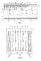
- Fig. 1 is a cross-sectional view for explaining a trench gate power MOSFET 1 according to an embodiment 1.
- Fig. 2 is a plan view for explaining the trench gate power MOSFET 1 according to the embodiment 1.
- the trench gate power MOSFET 1 according to the embodiment 1 is, as shown in Fig. 1 and Fig.
- n -type epitaxial layer semiconductor layer of first conductive type 12 formed on an upper surface of an n + -type silicon substrate 10
- a p-type body region body region of second conductive type 20 formed in the vicinity of an upper surface of the n -type epitaxial layer 12
- a plurality of trenches 14 formed such that the trenches 14 reach the n -type epitaxial layer 12 from an upper surface side of the p-type body region 20, and gates 18 respectively formed in the plurality of trenches 14.
- p-type carrier extracting regions 26a, 26b, 26c are formed in some regions out of regions of the n -type epitaxial layer 12 facing the p-type body region 20 in an opposed manner.
- numeral 22 indicates an n + -type source region
- numeral 24 indicates a p + -type contact region
- numeral 28 and numeral 29 indicate insulation layers
- numeral 32 indicates a source electrode
- numeral 34 indicates a drain electrode.
- the p-type carrier extracting regions 26a, 26b, 26c are formed in some regions out of regions of the n -type epitaxial layer 12 facing the p-type body region 20 in an opposed manner and hence, it is possible to form the p-type carrier extracting regions 26a, 26b, 26c at portions of a cell region where the collection of holes are required. Accordingly, the holes generated in the cell region can be efficiently collected through the p-type carrier extracting regions 26a, 26b, 26c thus providing a trench gate power MOSFET which can further accelerate a speed of the switching operation.
- the p-type carrier extracting region 26a which is present in the cell region is, as shown in Fig. 2 , formed such that the p-type carrier extracting regions 26a cover partial or whole regions of some trenches out of the plurality of trenches 14. Due to such constitution, the p-type carrier extracting regions 26a can be formed such that the p-type carrier extracting regions 26a cover the partial or whole regions of the trenches at portions where the collection of holes is required and hence, the holes can be efficiently collected. Further, also in this case, the p-type carrier extracting regions 26a can be formed only in the partial or whole regions of the necessary trenches out of the plurality of trenches 14 and hence, there is no possibility that the ON resistance is excessively increased.
- the p-type carrier extracting regions 26a are, as shown in Fig. 2 , formed such that the p-type carrier extracting regions 26a cover the whole regions of the outermost trenches out of the plurality of trenches 14. Due to such constitution, by forming the p-type carrier extracting regions 26a such that the p-type carrier extracting regions 26a cover the whole regions of some trenches at portions where the holes are liable to be easily generated, the holes can be further efficiently collected.
- the p-type carrier extracting regions 26b, 26c which are present in the peripheral region are, as shown in Fig. 1 and Fig. 2 , formed in a peripheral region outside the outermost trench out of the plurality of trenches 14. Due to such constitution, the p-type carrier extracting regions 26b, 26c are formed in the peripheral region which constitutes a region where a relatively large quantity of holes is generated and hence, the holes can be further efficiently collected.
- the p-type carrier extracting region 26b is formed on a lower surface side of the p-type body region 20, and the p-type carrier extracting region 26c is formed to cover the side surface of the p-type body region 20. Due to such constitution, the p-type carrier extracting regions 26b, 26c are respectively formed on the lower surface of the p-type body region 20 and on the side surface of the p-type body region 20 in the peripheral region which constitutes the region where a relatively large quantity of holes is generated and hence, the holes can be further efficiently collected.
- the p-type carrier extracting regions 26a, 26b, 26c are formed so as to reach a position of a depth larger than a depth of the trenches 14. Due to such constitution, the impingement of holes on the lower surface of the trench 14 is suppressed and hence, damages applied to a gate insulation film 16 formed in the vicinity of a bottom surface of the trench 14 can be suppressed.
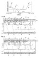
- Fig. 3 is a view showing an impurity concentration profile in the depth direction in the trench gate power MOSFET 1 according to the embodiment 1.
- the p-type carrier extracting region 26a is, as shown in Fig.3 , formed so as to reach a position deeper than the p-type body region 20. Further, the impurity concentration of the p-type carrier extracting region 26a is lower than the impurity concentration of the p-type body region 20. Due to such setting of the impurity concentration, the carrier extracting operation can be performed efficiently.
- Fig. 4 is a cross-sectional view for explaining a trench gate power MOSFET 2 according to an embodiment 2.
- the trench gate power MOSFET 2 according to the embodiment 2 basically has the structure considerably similar to the structure of the trench gate power MOSFET 1 according to the embodiment 1.
- the trench gate power MOSFET 2 according to the embodiment 2 differs from the trench gate power MOSFET 1 according to the embodiment 1 with respect to the constitution of the p-type carrier extracting regions present in the cell region. That is, in the trench gate power MOSFET 2 according to the embodiment 2, the p-type carrier extracting regions 26d present in the cell region are, as shown in Fig. 4 , formed in some inter-trench regions out of the inter-trench regions respectively sandwiched between two neighboring trenches out of the plurality of trenches 14.
- the trench gate power MOSFET 2 according to the embodiment 2 differs from the trench gate power MOSFET 1 according to the embodiment 1 with respect to the constitution of the p-type carrier extracting regions present in the cell region.
- the p-type carrier extracting regions 26d, 26b, 26c are formed in some regions out of the regions of the n -type epitaxial layer 12 facing the p-type body region 20 in an opposed manner and hence, it is possible to form the p-type carrier extracting regions 26d, 26b, 26c at portions of the cell region where the collection of holes is required. Accordingly, the holes generated in the cell region can be efficiently collected through the p-type carrier extracting regions 26d, 26b, 26c and hence, it is possible to provide the trench gate power MOSFET which can further accelerate a speed of the switching operation.
- the p-type carrier extracting regions 26d are formed in partial or whole regions of some inter-trench regions out of inter-trench regions which are respectively sandwiched between two neighboring trenches out of the plurality of trenches 14. Accordingly, the p-type carrier extracting regions 26d can be formed only in the regions where the collection of holes is required and hence, there is no possibility that the ON resistance is excessively increased.
- the p-type carrier extracting region 26d is formed in all regions respectively sandwiched between the outermost trench 14 out of the plurality of trenches 14 and the trench 14 arranged close to the outermost trench 14. Due to such constitution, the p-type carrier extracting region can be formed in all inter-trench regions at portions where the holes are liable to be easily generated and hence, the holes can be further efficiently collected.
- Fig. 5 is a cross-sectional view for explaining the trench gate power MOSFET 3 according to an embodiment 3.
- the trench gate power MOSFET 3 according to the embodiment 3 basically has the structure considerably similar to the structure of the trench gate power MOSFET 1 according to the embodiment 1.
- the trench gate power MOSFET 3 according to the embodiment 3 differs from the trench gate power MOSFET 1 according to the embodiment 1 with respect to the constitution of the p-type carrier extracting region present in the cell region. That is, in the trench gate power MOSFET 3 according to the embodiment 3, the p-type carrier extracting region 26e present in the cell region is, as shown in Fig. 5 , formed such that the p-type carrier extracting region 26e covers two neighboring trenches 14 out of the plurality of trenches 14 and an inter-trench region sandwiched between two neighboring trenches 14.
- the trench gate power MOSFET 3 according to the embodiment 3 differs from the trench gate power MOSFET 1 according to the embodiment 1 with respect to the constitution of the p-type carrier extracting region present in the cell region.
- the p-type carrier extracting regions 26e, 26b, 26c are formed in some regions out of the regions of the n -type epitaxial layer 12 facing the p-type body region 20 in an opposed manner and hence, it is possible to form the p-type carrier extracting regions 26e, 26b, 26c at portions of the cell region where the collection of holes is required. Accordingly, the holes generated in the cell region can be efficiently collected through the p-type carrier extracting regions 26e, 26b, 26c and hence, it is possible to provide the trench gate power MOSFET which can further accelerate a speed of the switching operation.
- the p-type carrier extracting region 26e is formed such that the p-type carrier extracting region 26e covers two neighboring trenches 14 out of the plurality of trenches 14 and the inter-trench region sandwiched between the two neighboring trenches 14. Accordingly, an area of the p-type carrier extracting region can be increased and hence, the holes can be efficiently collected.
- the trench gate power MOSFET 4 according to an embodiment 4 basically has the structure considerably similar to the structure of the trench gate power MOSFET 1 according to the embodiment 1. However, the trench gate power MOSFET 4 according to the embodiment 4 differs from the trench gate power MOSFET 1 according to the embodiment 1 with respect to the constitution of the p-type carrier extracting region present in the cell region.
- the p-type carrier extracting region present in the cell region includes all of p-type carrier extracting regions 26a, 26b, 26c, 26d, 26e respectively formed in the trench gate power MOSFET 1 according to the embodiment 1, in the trench gate power MOSFET 2 according to the embodiment 2 or in the trench gate power MOSFET 3 according to the embodiment 3.
- the trench gate power MOSFET 4 according to the embodiment 4 differs from the trench gate power MOSFETs 1, 2 and 3 according to the embodiments 1, 2 and 3 with respect to the constitution of the p-type carrier extracting region present in the cell region.
- the p-type carrier extracting regions are formed in some regions out of the regions of the n -type epitaxial layer 12 facing the p-type body region 20 in an opposed manner and hence, it is possible to form the p-type carrier extracting regions at portions of the cell region where the collection of holes is required. Accordingly, the holes generated in the cell region can be efficiently collected through the p-type carrier extracting regions and hence, it is possible to provide the trench gate power MOSFET which can further accelerate a speed of the switching operation.
- the p-type carrier extracting regions suitably selected from the above-mentioned p-type carrier extracting regions can be arranged at the portions where the collection of holes is required and hence, it is possible to arrange the p-type carrier extracting regions such that the holes can be further efficiently collected.
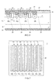
- Fig. 6 is a cross-sectional view for explaining a trench gate power MOSFET 5 according to an embodiment 5.
- Fig. 7 is a plan view for explaining the trench gate power MOSFET 5 according to the embodiment 5.
- the trench gate power MOSFET 5 is constituted of an n -type epitaxial layer (semiconductor layer of first conductive type) 12, a p-type body region (body region of second conductive type) 20 formed in the vicinity of an upper surface of the n -type epitaxial layer 12, a plurality of trenches 14 formed such that the trenches 14 reach the n -type epitaxial layer 12 from an upper surface side of the p-type body region 20, and gates 18 respectively formed in the plurality of trenches 14, wherein second trenches of a depth smaller than a depth of the p-type body region 20 and including a source electrode 38 formed on an upper surface of the p-type body region therein are formed in the p-type body region 20, and the p-type carrier extracting regions 36a, 36b are formed on lower surfaces of the second trenches such that the p-type carrier extracting regions 36a, 36b are connected to the source electrode 38 and reach the n -type epitaxial layer
- the second trenches are formed in the inter-trench regions and the p-type carrier extracting regions 36a, 36 are formed on the lower surfaces of the second trenches and hence, it is possible to form the p-type carrier extracting regions 36a at portions of the cell region where the collection of holes is required. Accordingly, the holes generated in the cell region can be efficiently collected through the p-type carrier extracting regions 36a thus providing a trench gate power MOSFET which can further accelerate a speed of the switching operation.
- the second trenches are, as shown in Fig. 6 , formed in all inter-trench regions which are respectively sandwiched between two neighboring trenches 14 out of the plurality of trenches 14. Due to such constitution, the p-type carrier extracting regions 36a can be formed over the whole surface of the cell region and hence, the holes can be efficiently collected. In this case, even when the p-type carrier extracting regions 36a are formed over the whole surface of the cell region, it is possible to prevent the carrier extracting regions from considerably ill-affecting a transistor operation and hence, there is no possibility that the switching performance is excessively lowered.
- the second trench is, as shown in Fig. 6 , also formed in the peripheral region further outside the outermost trench out of the plurality of trenches 14. Due to such constitution, the p-type carrier extracting region 36b is formed also in the peripheral region which constitutes a region where a relatively large quantity of holes is generated and hence, the holes can be further efficiently collected.
- the second trench formed in the peripheral region has a width larger than a width of the second trench formed in the cell region. Due to such constitution, by forming the p-type carrier extracting region 36b having a large area in the peripheral region which constitutes a region where a relatively large quantity of holes is generated, the holes generated in a relatively large quantity can be further efficiently collected.
- the p-type carrier extracting region 36b formed in the peripheral region is formed so as to reach a position deeper than the p-type carrier extracting region 36a formed in the cell region. Due to such constitution, by forming the deep p-type carrier extracting region 36b in the peripheral region where a relatively large quantity of holes is generated, the holes generated in a relatively large quantity can be further efficiently collected.
- the p-type carrier extracting region 36b is formed so as to reach a position of a depth larger than a depth of the trench 14. Due to such constitution, it is possible to prevent the impingement of holes on a lower surface of the trench 14 and hence, damages applied to the gate insulation film 16 formed in the vicinity of the bottom surface of the trench 14 can be suppressed.
- p + -type contact layers 24 for reducing contact resistance with the metal layer (source electrode 38) filled in the inside of the second trenches are formed. Due to such constitution, the holes collected by the p-type carrier extracting regions 36a, 36b can be efficiently discharged to the outside.
- Fig. 8 is a view showing an impurity concentration profile in the depth direction of the trench gate power MOSFET 5 according to the embodiment 5,
- the p-type carrier extracting region 36a is, as shown in Fig. 8 , formed so as to reach a position deeper than the p-type body region 20.
- the impurity concentration of the p-type carrier extracting region 36a is lower than the impurity concentration of the p-type body region 20.
- the impurity concentration of the p-type carrier extracting region 36a is higher than the impurity concentration of the p-type body region 20 at the p + -type contact layer 24. Due to such setting of the profile concentration, the carrier extracting operation can be performed efficiently.
- Fig. 9 is a plan view for explaining a trench gate power MOSFET 6 according to an embodiment 6.
- the trench gate power MOSFET 6 according to the embodiment 6 basically has the structure considerably similar to the structure of the trench gate power MOSFET 5 according to the embodiment 5.
- the trench gate power MOSFET 6 according to the embodiment 6 differs from the trench gate power MOSFET 5 according to the embodiment 5 with respect to a layout of the trenches 14. That is, in the trench gate power MOSFET 6 according to the embodiment 6, the trenches 14 have the lattice structure as shown in Fig. 9 .
- the trench gate power MOSFET 6 according to the embodiment 6 differs from the trench gate power MOSFET 5 according to the embodiment 5 with respect to the layout of the trenches 14, in the trench gate power MOSFET 6 according to the embodiment 6, the second trenches are formed in inter-trench regions and p-type carrier extracting regions 36a, 36b are also formed on lower surfaces of the second trenches and hence, it is possible to form the p-type carrier extracting regions 36a at positions in a cell region where the collection of holes is required. Accordingly, the holes generated in the cell region can be efficiently collected through the p-type carrier extracting regions 36a thus providing a trench gate power semiconductor device which can further accelerate a speed of the switching operation.
- a manufacturing method of a trench gate power MOSFET according to an embodiment 7 is a manufacturing method of manufacturing a trench gate power MOSFET provided for manufacturing the above-mentioned trench gate power MOSFET 4 according to the embodiment 4.
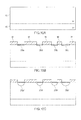
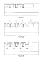
- Fig. 10 to Fig. 12 are views showing respective manufacturing steps of the method of manufacturing the trench gate power MOSFET according to the embodiment 7.
- the method of manufacturing the trench gate power MOSFET according to the embodiment 7 includes, as shown in Fig. 10 to Fig. 12 , following steps consisting of (a) a first step to (i) a ninth step executed in this order.
- the n + -type silicon substrate 10 which forms an n - -type epitaxial layer 12 on an upper surface thereof is prepared (see Fig. 10(a) ).
- the impurity concentration of the n - -type epitaxial layer 12 is, for example, 3x10 +15 atoms/cm 3 .
- a silicon oxide film M is selectively formed on a surface of the n - -type epitaxial layer 12.
- boron ions for example, 2.6 ⁇ 10 13 cm -2
- boron-ion-implanted layers 25a, 25d, 25b, 25c see Fig. 10(b) .
- thermal annealing is performed (for example, at a temperature of 1100°C for 100 minutes) thus forming the p-type diffusion layers 25a', 25d', 25b', 25c' which constitute the p-type carrier extracting regions (see Fig. 10(c) ).
- boron ions for example, 1.5 ⁇ 10 13 cm -2 ,50keV
- numeral 30 indicates a thermal oxidized film having a thickness of approximately 20 to 40nm.
- thermal annealing is performed (for example, at a temperature of 1100°C for 45 minutes) thus forming the p-type body region 20 (see Fig. 11(e) ).
- the p-type carrier extracting regions 26a, 26d, 26b, 26c are simultaneously formed.
- the trenches 14 are formed using a silicon oxide film (not shown in the drawing) as a mask.
- a gate insulation film 16 is formed on inner surfaces of the trenches 14 by thermal oxidation.
- the inside of the trenches is filled with polysilicon doped with phosphors, an upper surface of the polysilicon is etched back, and the upper surface is thermally oxidized to form gates 18 (see Fig. 11(f) ).
- boron ions for example, 2 ⁇ 10 14 cm -2
- thermal annealing is performed (for example, at a temperature of 900°C for 30 minutes) thus forming the p + -type contact regions 24 (see Fig. 12(g) ).
- arsenic ions for example, 4x10 15 cm -2
- thermal annealing is performed (for example, at a temperature of 1000°C for 10 minutes) thus forming the n + -type source regions 22 (see Fig. 12(h) ).
- insulation layers 28 are formed over the trenches and, at the same time, undesired insulation layers are removed. Thereafter, a source electrode 32 is formed over the insulation layers 28. Further, a drain electrode 34 is formed over a back surface of the n + -type silicon substrate 10 (see Fig. 12(i) ).
- the trench gate power MOSFET 4 according to the embodiment 4 can be manufactured. In this manner, according to the method of manufacturing the trench gate power MOSFET of the embodiment 7, it is possible to manufacture the trench gate power MOSFET 4 using the relatively simple method.
- Fig. 13 is a view showing respective manufacturing steps of a method of manufacturing a trench gate power MOSFET according to a modification of the embodiment 7.
- the method of manufacturing a trench gate power MOSFET according to the modification of the embodiment 7 is basically considerably similar to the method of manufacturing a trench gate power MOSFET according to the embodiment 7.
- the method of manufacturing a trench gate power MOSFET according to the modification of the embodiment 7 differs from the method of manufacturing a trench gate power MOSFET according to the embodiment 7 with respect to the second and third steps. That is, in the method of manufacturing a trench gate power MOSFET according to the modification of the embodiment 7, the second step and the third step are performed as follows.
- a silicon oxide film M is selectively formed on a surface of the n - -type epitaxial layer 12.
- boron ions are implanted in multiple stages (for example, 50keV to 2MeV) thus forming boron-ion-implanted layers 25a", 25d", 25b", 25c" (see Fig. 13 (b')).
- thermal annealing is performed (for example, at a temperature of 1000°C for 10 minutes) thus forming the p-type diffusion layers 25a"', 25d"', 25b"', 25c"' which constitute the p-type carrier extracting regions (see Fig. 13 (c')).
- the method of manufacturing a trench gate power MOSFET of the modification of the embodiment 7 by implanting the boron ions in multiple stages in second step, it is possible to form the p-type diffusion layers 25a"', 25d"', 25b"', 25c"' at a deep position due to thermal annealing performed in third step. Accordingly, the method of manufacturing a trench gate power MOSFET according to the modification of the embodiment 7 can acquire an advantageous effect that the p-type carrier extracting regions 26a, 26d, 26c, 26b deeper than the p-type body region 20 can be easily formed.
- a manufacturing method of a trench gate power MOSFET according to an embodiment 8 is a manufacturing method of manufacturing a trench gate power MOSFET provided for manufacturing the above-mentioned trench gate power MOSFET 5 according to the embodiment 5.
- Fig. 14 to Fig. 16 are views showing respective manufacturing steps of the method of manufacturing the trench gate power MOSFET according to the embodiment 8.
- the method of manufacturing the trench gate power MOSFET according to the embodiment 8, as shown in Fig. 14 to Fig. 16 includes following steps consisting of (a) a first step to (i) a ninth step executed in this order.
- the n + -type silicon substrate 10 which forms an n - -type epitaxial layer 12 on an upper surface thereof is prepared (see Fig. 14(a) ).
- the impurity concentration of the n - -type epitaxial layer 12 is, for example, 3 ⁇ 10 +15 atoms/cm 3 .
- an insulation layer 29 is selectively formed. Thereafter, using the insulation layer 29 as a mask, for example, boron ions (for example, 1.5 ⁇ 10 13 cm -2 ) are implanted from a surface of an n - -type epitaxial layer 12 and, thereafter, thermal annealing is performed (for example, at a temperature of 1100°C for 45 minutes) thus forming the p-type body region 20 (see Fig. 14(b) ).
- boron ions for example, 1.5 ⁇ 10 13 cm -2
- thermal annealing for example, at a temperature of 1100°C for 45 minutes
- a silicon oxide film (not shown in the drawing) is selectively formed on the surface of the n - -type epitaxial layer 12 and the trenches 14 are formed using the silicon oxide film as a mask.
- gate insulation films 16 are formed on inner surfaces of the trenches 14 by thermal oxidation. Thereafter, the inside of the trenches is filled with polysilicon doped with phosphors, an upper surface of the polysilicon is etched back, and the upper surface is thermally oxidized to form gates 18 (see Fig. 14(c) ).
- arsenic ions for example, 4 ⁇ 10 15 cm -2
- arsenic ions for example, 4 ⁇ 10 15 cm -2
- inter-trench regions respectively sandwiched between the trench 14 and the trench 14 thus forming arsenic ion implanted layers 21 (see Fig. 15(d) ).
- insulation layers 28 are formed and, using the insulation layers 28 as a mask, the second trenches are formed at predetermined positions in an intermediate region and a peripheral region in the inter-trench regions respectively sandwiched by the trenches 14 (see Fig. 15(e) ).
- boron ions for example, 2.6 ⁇ 10 15 cm -2
- boron-ion-implanted layers 35a, 35b see Fig. 15 (f) .
- thermal annealing is performed (for example, at a temperature of 1000°C for 10 minutes) thus forming the n + -type source regions 22 and the p-type carrier extracting regions 36a, 36b (see Fig. 16 (g) ).
- a source electrode 38 is formed over the insulation layers 28 (see Fig. 16(h) ).
- the inside of the second trenches is filled with metal which constitutes the source electrode 38.
- a drain electrode 34 is formed on a back surface of an n + -type silicon substrate 10 (see Fig. 16(i) ).
- the trench gate power MOSFET 5 according to the embodiment 5 can be manufactured. In this manner, according to the method of manufacturing the trench gate power MOSFET of the embodiment 8, it is possible to manufacture the trench gate power MOSFET 5 using the relatively simple method.
- the present invention is not limited to the above-mentioned respective embodiments, and the present invention can be exercised in various modes without departing from the gist of the present invention and, for example, following modifications also fall within the scope of the present invention.
- the present invention is explained by taking the trench gate power MOSFET as an example.
- the present invention is not limited to the trench gate power MOSFET and is also applicable to a trench gate IGBT.
- trench gate power MOSFET 10: n + -type silicon substrate, 12: n - -type epitaxial layer, 14: trench, 16: gate insulation film, 18: gate, 20: p-type body region, 22: n + -type source region, 24: p + -type contact region, 26a, 26b, 26c, 26d, 26e, 36a, 36b: p-type carrier extracting region, 28, 29: insulation layer, 30: thermal oxidization film, 32, 38: source electrode, 34: drain electrode, 900: trench gate power semiconductor device.
Landscapes
- Electrodes Of Semiconductors (AREA)
- Metal-Oxide And Bipolar Metal-Oxide Semiconductor Integrated Circuits (AREA)
Abstract
Description
- The present invention relates to a trench gate power semiconductor device.
-
Fig. 17 is a cross-sectional view of a conventional trench gatepower semiconductor device 900.
As shown inFig. 17 , the conventional trench gatepower semiconductor device 900 is a trench gate power semiconductor device which includes an n+-type epitaxial layer 911 (not shown in the drawing) formed in the vicinity of a p-type semiconductor substrate 910 (not shown in the drawing) and a surface of the p-type semiconductor substrate 910, an n--type epitaxial layer 912 (a semiconductor layer of first conductive type) arranged on the n+-type epitaxial layer 911, a p-type body region 920 (a body region of second conductive type) formed in the vicinity of an upper surface of the n--typeepitaxial layer 912, a plurality oftrenches 914 formed such that thetrenches 914 reach the n--typeepitaxial layer 912 from an upper surface side of the p-type body region 920, andgates 918 formed in the plurality oftrenches 914 by way ofgate insulation films 916.Emitter regions 922 are formed in the vicinity of an upper surface of the p-type body region 920 in an inter-trench region sandwiched between thetrenches 914. Aninsulation layer 928 is formed over thetrenches 914 and anemitter electrode 932 is formed over theinsulation layer 928. Further, a cathode electrode 934 (not shown in the drawing) is formed over a lower surface of the p-type semiconductor substrate 910. - In the conventional trench gate
power semiconductor device 900 having such a constitution, in a peripheral region GR which disposed further outside the outermostperipheral trench 914, a p-type semiconductor region 920a is formed such that the p-type semiconductor region 920a is connected to the p-type body region 920 and surrounds the p-type body region 920. The p-type semiconductor region 920a is formed deeper than the p-type body region 920 so as to maintain a high breakdown voltage thereof. The p-type semiconductor region 920a and the p-type body region 920 are connected to theemitter electrode 932 via contact holes CH formed in an upper surface of a side diffusion region SD and contact holes CH formed in an upper surface of a margin region MR adj acent to the side diffusion region SD. Theemitter regions 922 are not formed on the upper surface of the margin region MR. Here, inFig. 17 , a symbol CR indicates a cell region. - Due to such constitution, according to the conventional trench gate
power semiconductor device 900, most of the holes H generated in a relatively large quantity near the side diffusion region SD when a gate voltage is made to return from an ON voltage to an OFF voltage in theemitter electrode 932 pass through the side diffusion region SD and are collected by theemitter electrode 932 and hence, the holes can be speedily collected when the gate voltage is made to return to the OFF voltage thus accelerating a speed of the switching operation (for example, see patent document 1). - Patent document 1: Japan Published Unexamined Application No.
Hei 9-270512 Fig. 1 and Fig. 2 ) - The conventional trench gate
power semiconductor device 900 can collect the relatively large quantity of holes H generated in the vicinity of the side diffusion region SD of the peripheral region GR disposed further outside the outermostperipheral trench 914. However, when the gate voltage is made to return from the ON voltage to the OFF voltage, a certain quantity of holes although smaller in quantity compared to the holes generated in the vicinity of the side diffusion region SD is generated also in the cell region CR and hence, there arises a drawback that the further acceleration of a speed of the switching operation is impeded. - The present invention has been made to overcome the above-mentioned drawback, and it is an object of the present invention to provide a trench gate power semiconductor device capable of effectively collecting holes generated in a cell region so as to further accelerate a speed of the switching operation.
- (1) The present invention is directed to a trench gate power semiconductor device including a semiconductor layer of first conductive type, a body region of second conductive type opposite to the first conductive type, the body region formed in the vicinity of an upper surface of the semiconductor layer of first conductive type, a plurality of trenches formed so as to reach the semiconductor layer of first conductive type from an upper surface side of the body region of second conductive type, and gates formed in the plurality of trenches, wherein in some regions out of regions of the semiconductor layer of first conductive type facing the body region of second conductive type in an opposed manner, carrier extracting regions of second conductive type are formed.
- Due to such constitution, according to the trench gate power semiconductor device of the present invention, the carrier extracting regions of second conductive type are formed in some regions out of regions of the semiconductor layer of first conductive type facing the body region of second conductive type in an opposed manner and hence, it is possible to form the carrier extracting regions of second conductive type at portions of a cell region where the collection of holes are required. Accordingly, the holes generated in the cell region can be efficiently collected through the carrier extracting regions of second conductive type thus providing a trench gate power semiconductor device which can further accelerate a speed of the switching operation.
- (2) In the trench gate power semiconductor device having the constitution (1), the carrier extracting regions of second conductive type may preferably be formed such that the carrier extracting regions cover partial or whole regions of some trenches out of the plurality of trenches.
- Due to such constitution, the carrier extracting region of second conductive type can be formed such that the carrier extracting region covers the partial or whole region of the trenches at portions where the collection of holes is required and hence, the holes can be efficiently collected. Further, also in this case, the carrier extracting region of second conductive type can be formed only in the partial or whole region of the necessary trenches out of the plurality of trenches and hence, there is no possibility that the ON resistance is excessively increased.
- (3) In the trench gate power semiconductor device having the constitution (2), the carrier extracting region of second conductive type may preferably be formed such that the carrier extracting region covers a partial or whole region of the outermost trench out of the plurality of trenches.
- Due to such constitution, the carrier extracting region of second conductive type can be formed such that the carrier extracting region covers the partial or whole region of some trenches at portions where the holes are liable to be easily generated and hence, the holes can be further efficiently collected.
- (4) In the trench gate power semiconductor device having the constitution (1), the carrier extracting regions of second conductive type may preferably be formed in partial or whole regions of some inter-trench regions out of inter-trench regions which are respectively sandwiched between two neighboring trenches out of the plurality of trenches.
- Also due to such constitution, the carrier extracting region of second conductive type can be formed in the partial or whole regions of the inter-trench regions at portions where the collection of holes is required and hence, the holes can be efficiently collected. Also in this case, the carrier extracting region of second conductive type can be formed only in the partial or whole regions of necessary inter-trench regions out of the plurality of inter-trench regions and hence, there is no possibility that the ON resistance is excessively increased.
- (5) In the trench gate power semiconductor device having the constitution (4), the carrier extracting region of second conductive type may preferably be formed in a partial or whole region of the inter-trench region sandwiched between the outermost trench out of the plurality of trenches and the trench arranged close to the outermost trench.
- Due to such constitution, the carrier extracting region of second conductive type can be formed in the partial or whole regions of some inter-trench regions at portions where the holes are liable to be easily generated and hence, the holes can be further efficiently collected.
- (6) In the trench gate power semiconductor device having the constitution (1), the carrier extracting region of second conductive type may preferably be formed such that the carrier extracting region covers two neighboring trenches out of the plurality of trenches and an inter-trench region sandwiched between the two neighboring trenches.
- Due to such constitution, an area of the carrier extracting region of second conductive type can be increased and hence, the holes can be efficiently collected.
- (7) In the trench gate power semiconductor device having any one of the constitutions (2) to (6), the carrier extracting region of second conductive type may preferably be also formed in a peripheral region outside the outermost trench out of the plurality of trenches.
- Due to such constitution, the carrier extracting region of second conductive type is formed also in the peripheral region which constitutes a region where a relatively large quantity of holes is generated and hence, the holes can be further efficiently collected.
- (8) In the trench gate power semiconductor device having the constitution (7), the carrier extracting region of second conductive type formed in the peripheral region may preferably be formed on a lower surface side of the body region of second conductive type.
- Due to such constitution, the carrier extracting region of second conductive type is formed on the lower surface of the body region of second conductive type in the peripheral region which constitutes the region where a relatively large quantity of holes is generated and hence, the holes can be further efficiently collected.
- (9) In the trench gate power semiconductor device having the constitutions (7) or (8), the carrier extracting region of second conductive type formed in the peripheral region may preferably be formed such that the carrier extracting region covers a side surface of the body region of second conductive type.
- Due to such constitution, the carrier extracting region of second conductive type is formed such that the carrier extracting region covers the side surface of the body region of second conductive type in the peripheral region which constitutes the region where a relatively large quantity of holes is generated and hence, the holes can be further efficiently collected.
- (10) In the trench gate power semiconductor device having any one of the constitutions (1) to (9), the carrier extracting region of second conductive type may preferably be formed so as to reach a position of a depth larger than a depth of the trenches.
- Due to such constitution, the impingement of holes on the lower surface of the trench can be suppressed and hence, damages applied to a gate insulation film formed in the vicinity of a bottom surface of the trench can be suppressed.
- (11) The present invention is directed to a trench gate power semiconductor device including a semiconductor layer of first conductive type, a body region of second conductive type opposite to the first conductive type, the body region formed in the vicinity of an upper surface of the semiconductor layer of first conductive type, a plurality of trenches formed so as to reach the semiconductor layer of first conductive type from an upper surface side of the body region of second conductive type, and gates formed in the plurality of trenches, wherein a second trench of a depth smaller than a depth of the body region of second conductive type and including a metal layer connected with an electrode different from a gate electrode out of electrodes formed on an upper surface of the semiconductor layer of first conductive type therein is formed in the body region of second conductive type, and a carrier extracting region of second conductive type is formed on a lower surface of the second trench such that the carrier extracting region is connected to the metal layer and reaches the semiconductor layer of first conductive type.
- Due to such constitution, according to another trench gate power semiconductor device of the present invention, the second trench is formed in the inter-trench region and the carrier extracting region of second conductive type is formed on the lower surface of the second trench and hence, the carrier extracting region of second conductive type can be formed at a portion of a cell region where the collection of holes is required. Accordingly, the holes generated in the cell region can be efficiently collected through the carrier extracting region of second conductive type and hence, it is possible to provide the trench gate power semiconductor device which can further accelerate a speed of the switching operation.
- (12) In the trench gate power semiconductor device having the constitution (11), the secondtrenchmaypreferablybe formed in all inter-trench regions which are respectively sandwiched between two neighboring trenches out of the plurality of trenches.
- Due to such constitution, the carrier extracting region of second conductive type can be formed over the whole surface of the cell region and hence, the holes can be efficiently collected. In this case, even when the carrier extracting region of second conductive type is formed over the whole surface of the cell region, it is possible to prevent the carrier extracting region from considerably ill-affecting a transistor operation and hence, there is no possibility that the switching performance is excessively lowered.
- (13) In the trench gate power semiconductor device having the constitution (11), the secondtrenchmaypreferablybe formed in some regions out of all inter-trench regions which are respectively sandwiched between two neighboring trenches out of the plurality of trenches.
- Due to such constitution, the carrier extracting region of second conductive type can be formed only at necessary portions of the cell region and hence, the adverse influence exerted on a transistor operation can be minimized.
- (14) In the trench gate power semiconductor device having the constitution (11), the secondtrenchmaypreferablybe formed in partial or whole regions of some inter-trench regions out of inter-trench regions which are respectively sandwiched between two neighboring trenches out of the plurality of trenches.
- Also due to such constitution, the carrier extracting region of second conductive type can be formed only at necessary portions of the cell region and hence, the adverse influence exerted on a transistor operation can be minimized.
- (15) In the trench gate power semiconductor device having the constitution (11), the second trench may preferably be formed in a peripheral region further outside the outermost trench out of the plurality of trenches.
- Due to such constitution, the carrier extracting region of second conductive type is formed in the peripheral region which constitutes a region where a relatively large quantity of holes is generated and hence, the holes can be further efficiently collected.
- (16) In the trench gate power semiconductor device having any one of the constitutions (12) to (14), the second trench may preferably be formed in a peripheral region further outside the outermost trench out of the plurality of trenches.
- Due to such constitution, the carrier extracting region of second conductive type is also formed in the peripheral region which constitutes a region where a relatively large quantity of holes is generated and hence, the holes can be further efficiently collected.
- (17) In the trench gate power semiconductor device having the constitution (16), the second trench formed in the peripheral region may preferably have a width larger than a width of the second trench formed in the inter-trench region.
- Due to such constitution, the carrier extracting region of second conductive type having a large area is formed in the peripheral region which constitutes a region where a relatively large quantity of holes is generated and hence, the holes which are generated in a relatively large quantity can be further efficiently collected.
- (18) In the trench gate power semiconductor device having the constitutions (16) or (17), the carrier extracting region of second conductive type formed in the peripheral region may preferably be formed so as to reach a position deeper than the carrier extracting region of second conductive type formed in the inter-trench region.
- Due to such constitution, the deep carrier extracting region of second conductive type is formed in the peripheral region which constitutes a region where a relatively large quantity of holes is generated and hence, the holes which are generated in a relatively large quantity can be further efficiently collected.
- (19) In the trench gate power semiconductor device having any one of the constitutions (11) to (18), the carrier extracting region of second conductive type may preferably be formed so as to reach a position of a depth larger than a depth of the trench.
- Due to such constitution, the impingement of holes on the lower surface of the trench can be suppressed and hence, damages applied to a gate insulation film formed in the vicinity of a bottom surface of the trench can be suppressed.
- (20) In the trench gate power semiconductor device having any one of the constitutions (11) to (19), on a portion of the carrier extracting region of second conductive type which is brought into contact with the second trench, a contact layer for reducing contact resistance with the metal layer filled in the inside of the second trench may preferably be formed.
- Due to such constitution, the holes collected by the carrier extracting region of second conductive type can be efficiently discharged to the outside.
- (21) In the trench gate power semiconductor device having any one of the constitutions (1) to (20), the trench gate power semiconductor device may be a power MOSFET.
- Due to such constitution, it is possible to provide a trench gate power MOSFET which can further accelerate a speed of the switching operation.
- (22) In the trench gate power semiconductor device having any one of the constitutions (1) to (20), the trench gate power semiconductor device may be an IGBT.
- Due to such constitution, it is possible to provide a trench gate IGBT which can further accelerate a speed of the switching operation.
-
-
Fig. 1 is a cross-sectional view for explaining a trenchgate power MOSFET 1 according to anembodiment 1. -
Fig. 2 is a plan view for explaining the trenchgate power MOSFET 1 according to theembodiment 1. -
Fig. 3 is a view showing an impurity concentration profile in the depth direction in the trenchgate power MOSFET 1 according to theembodiment 1. -
Fig. 4 is a cross-sectional view for explaining a trenchgate power MOSFET 2 according to anembodiment 2. -
Fig. 5 is a cross-sectional view for explaining a trenchgate power MOSFET 3 according to anembodiment 3. -
Fig. 6 is a cross-sectional view for explaining a trenchgate power MOSFET 5 according to anembodiment 5. -
Fig. 7 is a plan view for explaining the trenchgate power MOSFET 5 according to theembodiment 5. -
Fig. 8 is a view showing an impurity concentration profile in the depth direction in the trenchgate power MOSFET 5 according to theembodiment 5. -
Fig. 9 is a plan view for explaining a trenchgate power MOSFET 6 according to anembodiment 6. -
Fig. 10 is a view showing respective manufacturing steps of a manufacturing method of a trench gate power MOSFET according to an embodiment 7. -
Fig. 11 is a view showing respective manufacturing steps of the manufacturing method of the trench gate power MOSFET according to the embodiment 7. -
Fig. 12 is a view showing respective manufacturing steps of the manufacturing method of the trench gate power MOSFET according to the embodiment 7. -
Fig. 13 is a view showing respective manufacturing steps of the manufacturing method of a trench gate power MOSFET according to a modification of the embodiment 7. -
Fig. 14 is a view showing respective manufacturing steps of a manufacturing method of a trench gate power MOSFET according to an embodiment 8. -
Fig. 15 is a view showing respective manufacturing steps of the manufacturing method of the trench gate power MOSFET according to the embodiment 8. -
Fig. 16 is a view showing respective manufacturing steps of the manufacturing method of the trench gate power MOSFET according to the embodiment 8. -
Fig. 17 is a cross-sectional view of a conventional trench gatepower semiconductor device 900. - Embodiments of the present invention are explained in detail in conjunction with drawings hereinafter.
-
Fig. 1 is a cross-sectional view for explaining a trenchgate power MOSFET 1 according to anembodiment 1.Fig. 2 is a plan view for explaining the trenchgate power MOSFET 1 according to theembodiment 1.
The trenchgate power MOSFET 1 according to theembodiment 1 is, as shown inFig. 1 and Fig. 2 , constituted of an n -type epitaxial layer (semiconductor layer of first conductive type) 12 formed on an upper surface of an n+-type silicon substrate 10, a p-type body region (body region of second conductive type) 20 formed in the vicinity of an upper surface of the n -type epitaxial layer 12, a plurality oftrenches 14 formed such that thetrenches 14 reach the n -type epitaxial layer 12 from an upper surface side of the p-type body region 20, andgates 18 respectively formed in the plurality oftrenches 14. Further, p-typecarrier extracting regions type epitaxial layer 12 facing the p-type body region 20 in an opposed manner. InFig. 1 , numeral 22 indicates an n+-type source region, numeral 24indicates a p+-type contact region, numeral 28 and numeral 29 indicate insulation layers, numeral 32 indicates a source electrode, and numeral 34 indicates a drain electrode. - Due to such constitution, according to the trench
gate power MOSFET 1 of theembodiment 1, the p-typecarrier extracting regions type epitaxial layer 12 facing the p-type body region 20 in an opposed manner and hence, it is possible to form the p-typecarrier extracting regions carrier extracting regions - Out of the p-type
carrier extracting regions carrier extracting region 26a which is present in the cell region is, as shown inFig. 2 , formed such that the p-typecarrier extracting regions 26a cover partial or whole regions of some trenches out of the plurality oftrenches 14.
Due to such constitution, the p-typecarrier extracting regions 26a can be formed such that the p-typecarrier extracting regions 26a cover the partial or whole regions of the trenches at portions where the collection of holes is required and hence, the holes can be efficiently collected. Further, also in this case, the p-typecarrier extracting regions 26a can be formed only in the partial or whole regions of the necessary trenches out of the plurality oftrenches 14 and hence, there is no possibility that the ON resistance is excessively increased. - Further, the p-type
carrier extracting regions 26a are, as shown inFig. 2 , formed such that the p-typecarrier extracting regions 26a cover the whole regions of the outermost trenches out of the plurality oftrenches 14.
Due to such constitution, by forming the p-typecarrier extracting regions 26a such that the p-typecarrier extracting regions 26a cover the whole regions of some trenches at portions where the holes are liable to be easily generated, the holes can be further efficiently collected. - Out of the p-type
carrier extracting regions carrier extracting regions Fig. 1 and Fig. 2 , formed in a peripheral region outside the outermost trench out of the plurality oftrenches 14.
Due to such constitution, the p-typecarrier extracting regions - Here, the p-type
carrier extracting region 26b is formed on a lower surface side of the p-type body region 20, and the p-typecarrier extracting region 26c is formed to cover the side surface of the p-type body region 20.
Due to such constitution, the p-typecarrier extracting regions type body region 20 and on the side surface of the p-type body region 20 in the peripheral region which constitutes the region where a relatively large quantity of holes is generated and hence, the holes can be further efficiently collected. - Further, in the trench
gate power MOSFET 1 according to theembodiment 1, the p-typecarrier extracting regions trenches 14.
Due to such constitution, the impingement of holes on the lower surface of thetrench 14 is suppressed and hence, damages applied to agate insulation film 16 formed in the vicinity of a bottom surface of thetrench 14 can be suppressed. -
Fig. 3 is a view showing an impurity concentration profile in the depth direction in the trenchgate power MOSFET 1 according to theembodiment 1.
In the trenchgate power MOSFET 1 according to theembodiment 1, the p-typecarrier extracting region 26a is, as shown inFig.3 , formed so as to reach a position deeper than the p-type body region 20. Further, the impurity concentration of the p-typecarrier extracting region 26a is lower than the impurity concentration of the p-type body region 20. Due to such setting of the impurity concentration, the carrier extracting operation can be performed efficiently. -
Fig. 4 is a cross-sectional view for explaining a trenchgate power MOSFET 2 according to anembodiment 2.
The trenchgate power MOSFET 2 according to theembodiment 2 basically has the structure considerably similar to the structure of the trenchgate power MOSFET 1 according to theembodiment 1. However, the trenchgate power MOSFET 2 according to theembodiment 2 differs from the trenchgate power MOSFET 1 according to theembodiment 1 with respect to the constitution of the p-type carrier extracting regions present in the cell region. That is, in the trenchgate power MOSFET 2 according to theembodiment 2, the p-typecarrier extracting regions 26d present in the cell region are, as shown inFig. 4 , formed in some inter-trench regions out of the inter-trench regions respectively sandwiched between two neighboring trenches out of the plurality oftrenches 14. - In this manner, the trench
gate power MOSFET 2 according to theembodiment 2 differs from the trenchgate power MOSFET 1 according to theembodiment 1 with respect to the constitution of the p-type carrier extracting regions present in the cell region. However, the p-typecarrier extracting regions type epitaxial layer 12 facing the p-type body region 20 in an opposed manner and hence, it is possible to form the p-typecarrier extracting regions carrier extracting regions - Further, in the trench
gate power MOSFET 2 according to theembodiment 2, the p-typecarrier extracting regions 26d are formed in partial or whole regions of some inter-trench regions out of inter-trench regions which are respectively sandwiched between two neighboring trenches out of the plurality oftrenches 14. Accordingly, the p-typecarrier extracting regions 26d can be formed only in the regions where the collection of holes is required and hence, there is no possibility that the ON resistance is excessively increased. - Further, in the trench
gate power MOSFET 2 according to theembodiment 2, although not shown explicitly inFig. 4 , the p-typecarrier extracting region 26d is formed in all regions respectively sandwiched between theoutermost trench 14 out of the plurality oftrenches 14 and thetrench 14 arranged close to theoutermost trench 14.
Due to such constitution, the p-type carrier extracting region can be formed in all inter-trench regions at portions where the holes are liable to be easily generated and hence, the holes can be further efficiently collected. -
Fig. 5 is a cross-sectional view for explaining the trenchgate power MOSFET 3 according to anembodiment 3.
The trenchgate power MOSFET 3 according to theembodiment 3 basically has the structure considerably similar to the structure of the trenchgate power MOSFET 1 according to theembodiment 1. However, the trenchgate power MOSFET 3 according to theembodiment 3 differs from the trenchgate power MOSFET 1 according to theembodiment 1 with respect to the constitution of the p-type carrier extracting region present in the cell region. That is, in the trenchgate power MOSFET 3 according to theembodiment 3, the p-typecarrier extracting region 26e present in the cell region is, as shown inFig. 5 , formed such that the p-typecarrier extracting region 26e covers two neighboringtrenches 14 out of the plurality oftrenches 14 and an inter-trench region sandwiched between two neighboringtrenches 14. - In this manner, the trench
gate power MOSFET 3 according to theembodiment 3 differs from the trenchgate power MOSFET 1 according to theembodiment 1 with respect to the constitution of the p-type carrier extracting region present in the cell region. However, the p-typecarrier extracting regions type epitaxial layer 12 facing the p-type body region 20 in an opposed manner and hence, it is possible to form the p-typecarrier extracting regions carrier extracting regions - Further, according to the trench
gate power MOSFET 3 of theembodiment 3, as described above, the p-typecarrier extracting region 26e is formed such that the p-typecarrier extracting region 26e covers two neighboringtrenches 14 out of the plurality oftrenches 14 and the inter-trench region sandwiched between the two neighboringtrenches 14. Accordingly, an area of the p-type carrier extracting region can be increased and hence, the holes can be efficiently collected. - The trench
gate power MOSFET 4 according to an embodiment 4 (not shown in the drawing) basically has the structure considerably similar to the structure of the trenchgate power MOSFET 1 according to theembodiment 1. However, the trenchgate power MOSFET 4 according to theembodiment 4 differs from the trenchgate power MOSFET 1 according to theembodiment 1 with respect to the constitution of the p-type carrier extracting region present in the cell region. That is, in the trenchgate power MOSFET 4 according to theembodiment 4, the p-type carrier extracting region present in the cell region includes all of p-typecarrier extracting regions gate power MOSFET 1 according to theembodiment 1, in the trenchgate power MOSFET 2 according to theembodiment 2 or in the trenchgate power MOSFET 3 according to theembodiment 3. - In this manner, the trench
gate power MOSFET 4 according to theembodiment 4 differs from the trenchgate power MOSFETs embodiments type epitaxial layer 12 facing the p-type body region 20 in an opposed manner and hence, it is possible to form the p-type carrier extracting regions at portions of the cell region where the collection of holes is required. Accordingly, the holes generated in the cell region can be efficiently collected through the p-type carrier extracting regions and hence, it is possible to provide the trench gate power MOSFET which can further accelerate a speed of the switching operation. - Further, according to the trench
gate power MOSFET 4 of theembodiment 4, the p-type carrier extracting regions suitably selected from the above-mentioned p-type carrier extracting regions can be arranged at the portions where the collection of holes is required and hence, it is possible to arrange the p-type carrier extracting regions such that the holes can be further efficiently collected. -
Fig. 6 is a cross-sectional view for explaining a trenchgate power MOSFET 5 according to anembodiment 5.Fig. 7 is a plan view for explaining the trenchgate power MOSFET 5 according to theembodiment 5. - The trench
gate power MOSFET 5 according to theembodiment 5 is constituted of an n -type epitaxial layer (semiconductor layer of first conductive type) 12, a p-type body region (body region of second conductive type) 20 formed in the vicinity of an upper surface of the n -type epitaxial layer 12, a plurality oftrenches 14 formed such that thetrenches 14 reach the n -type epitaxial layer 12 from an upper surface side of the p-type body region 20, andgates 18 respectively formed in the plurality oftrenches 14, wherein second trenches of a depth smaller than a depth of the p-type body region 20 and including asource electrode 38 formed on an upper surface of the p-type body region therein are formed in the p-type body region 20, and the p-typecarrier extracting regions carrier extracting regions source electrode 38 and reach the n -type epitaxial layer 12. - Due to such constitution, according to the trench
gate power MOSFET 5 of theembodiment 5, the second trenches are formed in the inter-trench regions and the p-typecarrier extracting regions 36a, 36 are formed on the lower surfaces of the second trenches and hence, it is possible to form the p-typecarrier extracting regions 36a at portions of the cell region where the collection of holes is required. Accordingly, the holes generated in the cell region can be efficiently collected through the p-typecarrier extracting regions 36a thus providing a trench gate power MOSFET which can further accelerate a speed of the switching operation. - In the trench
gate power MOSFET 5 according to theembodiment 5, the second trenches are, as shown inFig. 6 , formed in all inter-trench regions which are respectively sandwiched between two neighboringtrenches 14 out of the plurality oftrenches 14.
Due to such constitution, the p-typecarrier extracting regions 36a can be formed over the whole surface of the cell region and hence, the holes can be efficiently collected. In this case, even when the p-typecarrier extracting regions 36a are formed over the whole surface of the cell region, it is possible to prevent the carrier extracting regions from considerably ill-affecting a transistor operation and hence, there is no possibility that the switching performance is excessively lowered. - Further, in the trench
gate power MOSFET 5 according to theembodiment 5, the second trench is, as shown inFig. 6 , also formed in the peripheral region further outside the outermost trench out of the plurality oftrenches 14.
Due to such constitution, the p-typecarrier extracting region 36b is formed also in the peripheral region which constitutes a region where a relatively large quantity of holes is generated and hence, the holes can be further efficiently collected. - Further, in the trench
gate power MOSFET 5 according to theembodiment 5, the second trench formed in the peripheral region has a width larger than a width of the second trench formed in the cell region.
Due to such constitution, by forming the p-typecarrier extracting region 36b having a large area in the peripheral region which constitutes a region where a relatively large quantity of holes is generated, the holes generated in a relatively large quantity can be further efficiently collected. - Further, in the trench
gate power MOSFET 5 according to theembodiment 5, the p-typecarrier extracting region 36b formed in the peripheral region is formed so as to reach a position deeper than the p-typecarrier extracting region 36a formed in the cell region.
Due to such constitution, by forming the deep p-typecarrier extracting region 36b in the peripheral region where a relatively large quantity of holes is generated, the holes generated in a relatively large quantity can be further efficiently collected. - Further, in the trench
gate power MOSFET 5 according to theembodiment 5, the p-typecarrier extracting region 36b is formed so as to reach a position of a depth larger than a depth of thetrench 14.
Due to such constitution, it is possible to prevent the impingement of holes on a lower surface of thetrench 14 and hence, damages applied to thegate insulation film 16 formed in the vicinity of the bottom surface of thetrench 14 can be suppressed. - Further, in the trench
gate power MOSFET 5 according to theembodiment 5, on portions of the p-typecarrier extracting regions
Due to such constitution, the holes collected by the p-typecarrier extracting regions -
Fig. 8 is a view showing an impurity concentration profile in the depth direction of the trenchgate power MOSFET 5 according to theembodiment 5,
In the trenchgate power MOSFET 5 according to theembodiment 5, the p-typecarrier extracting region 36a is, as shown inFig. 8 , formed so as to reach a position deeper than the p-type body region 20. Further, the impurity concentration of the p-typecarrier extracting region 36a is lower than the impurity concentration of the p-type body region 20. However, the impurity concentration of the p-typecarrier extracting region 36a is higher than the impurity concentration of the p-type body region 20 at the p+-type contact layer 24. Due to such setting of the profile concentration, the carrier extracting operation can be performed efficiently. -
Fig. 9 is a plan view for explaining a trenchgate power MOSFET 6 according to anembodiment 6.
The trenchgate power MOSFET 6 according to theembodiment 6 basically has the structure considerably similar to the structure of the trenchgate power MOSFET 5 according to theembodiment 5. However, the trenchgate power MOSFET 6 according to theembodiment 6 differs from the trenchgate power MOSFET 5 according to theembodiment 5 with respect to a layout of thetrenches 14. That is, in the trenchgate power MOSFET 6 according to theembodiment 6, thetrenches 14 have the lattice structure as shown inFig. 9 . - Although the trench
gate power MOSFET 6 according to theembodiment 6 differs from the trenchgate power MOSFET 5 according to theembodiment 5 with respect to the layout of thetrenches 14, in the trenchgate power MOSFET 6 according to theembodiment 6, the second trenches are formed in inter-trench regions and p-typecarrier extracting regions carrier extracting regions 36a at positions in a cell region where the collection of holes is required. Accordingly, the holes generated in the cell region can be efficiently collected through the p-typecarrier extracting regions 36a thus providing a trench gate power semiconductor device which can further accelerate a speed of the switching operation. - A manufacturing method of a trench gate power MOSFET according to an embodiment 7 is a manufacturing method of manufacturing a trench gate power MOSFET provided for manufacturing the above-mentioned trench
gate power MOSFET 4 according to theembodiment 4. -
Fig. 10 to Fig. 12 are views showing respective manufacturing steps of the method of manufacturing the trench gate power MOSFET according to the embodiment 7.
The method of manufacturing the trench gate power MOSFET according to the embodiment 7 includes, as shown inFig. 10 to Fig. 12 , following steps consisting of (a) a first step to (i) a ninth step executed in this order. - The n+-
type silicon substrate 10 which forms an n--type epitaxial layer 12 on an upper surface thereof is prepared (seeFig. 10(a) ). The impurity concentration of the n--type epitaxial layer 12 is, for example, 3x10+15 atoms/cm3. - Next, a silicon oxide film M is selectively formed on a surface of the n--
type epitaxial layer 12. Using the silicon oxide film M as a mask, for example, boron ions (for example, 2.6×1013cm-2) are implanted thus forming boron-ion-implantedlayers Fig. 10(b) ). - Next, thermal annealing is performed (for example, at a temperature of 1100°C for 100 minutes) thus forming the p-
type diffusion layers 25a', 25d', 25b', 25c' which constitute the p-type carrier extracting regions (seeFig. 10(c) ). - Next, after removing the silicon oxide film M, using an
insulation film 2 9 as a mask, for example, boron ions (for example, 1.5×1013cm-2,50keV) are implanted thus forming a boron-ion-implanted layer 19 (seeFig. 11(d) ). Here, numeral 30 indicates a thermal oxidized film having a thickness of approximately 20 to 40nm. - Next, thermal annealing is performed (for example, at a temperature of 1100°C for 45 minutes) thus forming the p-type body region 20 (see
Fig. 11(e) ). Here, the p-typecarrier extracting regions - Next, the
trenches 14 are formed using a silicon oxide film (not shown in the drawing) as a mask. After removing the silicon oxide film, agate insulation film 16 is formed on inner surfaces of thetrenches 14 by thermal oxidation. Thereafter, the inside of the trenches is filled with polysilicon doped with phosphors, an upper surface of the polysilicon is etched back, and the upper surface is thermally oxidized to form gates 18 (seeFig. 11(f) ). - Next, for example, boron ions (for example, 2×1014cm-2) are implanted in portions which are expected to become the p+-
type contact regions 24 and, thereafter, thermal annealing is performed (for example, at a temperature of 900°C for 30 minutes) thus forming the p+-type contact regions 24 (seeFig. 12(g) ). - Next, for example, arsenic ions (for example, 4x1015cm-2) are implanted to portions corresponding to the n+-
type source regions 22. Thereafter, thermal annealing is performed (for example, at a temperature of 1000°C for 10 minutes) thus forming the n+-type source regions 22 (seeFig. 12(h) ). - Next, insulation layers 28 are formed over the trenches and, at the same time, undesired insulation layers are removed. Thereafter, a
source electrode 32 is formed over the insulation layers 28. Further, adrain electrode 34 is formed over a back surface of the n+-type silicon substrate 10 (seeFig. 12(i) ). - According to the method of manufacturing a trench gate power MOSFET according to the embodiment 7, by performing the above-mentioned steps, the trench
gate power MOSFET 4 according to theembodiment 4 can be manufactured. In this manner, according to the method of manufacturing the trench gate power MOSFET of the embodiment 7, it is possible to manufacture the trenchgate power MOSFET 4 using the relatively simple method. -
Fig. 13 is a view showing respective manufacturing steps of a method of manufacturing a trench gate power MOSFET according to a modification of the embodiment 7.
The method of manufacturing a trench gate power MOSFET according to the modification of the embodiment 7 is basically considerably similar to the method of manufacturing a trench gate power MOSFET according to the embodiment 7. However, the method of manufacturing a trench gate power MOSFET according to the modification of the embodiment 7 differs from the method of manufacturing a trench gate power MOSFET according to the embodiment 7 with respect to the second and third steps. That is, in the method of manufacturing a trench gate power MOSFET according to the modification of the embodiment 7, the second step and the third step are performed as follows. - A silicon oxide film M is selectively formed on a surface of the n--
type epitaxial layer 12. Using the silicon oxide film M as a mask, for example, boron ions are implanted in multiple stages (for example, 50keV to 2MeV) thus forming boron-ion-implantedlayers 25a", 25d", 25b", 25c" (seeFig. 13 (b')). - Next, thermal annealing is performed (for example, at a temperature of 1000°C for 10 minutes) thus forming the p-type diffusion layers 25a"', 25d"', 25b"', 25c"' which constitute the p-type carrier extracting regions (see
Fig. 13 (c')). - In this manner, according to the method of manufacturing a trench gate power MOSFET of the modification of the embodiment 7, by implanting the boron ions in multiple stages in second step, it is possible to form the p-type diffusion layers 25a"', 25d"', 25b"', 25c"' at a deep position due to thermal annealing performed in third step. Accordingly, the method of manufacturing a trench gate power MOSFET according to the modification of the embodiment 7 can acquire an advantageous effect that the p-type
carrier extracting regions type body region 20 can be easily formed. - A manufacturing method of a trench gate power MOSFET according to an embodiment 8 is a manufacturing method of manufacturing a trench gate power MOSFET provided for manufacturing the above-mentioned trench
gate power MOSFET 5 according to theembodiment 5. -
Fig. 14 to Fig. 16 are views showing respective manufacturing steps of the method of manufacturing the trench gate power MOSFET according to the embodiment 8.
The method of manufacturing the trench gate power MOSFET according to the embodiment 8, as shown inFig. 14 to Fig. 16 , includes following steps consisting of (a) a first step to (i) a ninth step executed in this order. - The n+-
type silicon substrate 10 which forms an n--type epitaxial layer 12 on an upper surface thereof is prepared (seeFig. 14(a) ). The impurity concentration of the n--type epitaxial layer 12 is, for example, 3×10+15 atoms/cm3. - Next, an
insulation layer 29 is selectively formed. Thereafter, using theinsulation layer 29 as a mask, for example, boron ions (for example, 1.5×1013cm-2) are implanted from a surface of an n--type epitaxial layer 12 and, thereafter, thermal annealing is performed (for example, at a temperature of 1100°C for 45 minutes) thus forming the p-type body region 20 (seeFig. 14(b) ). - Next, a silicon oxide film (not shown in the drawing) is selectively formed on the surface of the n--
type epitaxial layer 12 and thetrenches 14 are formed using the silicon oxide film as a mask. After removing the silicon oxide film,gate insulation films 16 are formed on inner surfaces of thetrenches 14 by thermal oxidation. Thereafter, the inside of the trenches is filled with polysilicon doped with phosphors, an upper surface of the polysilicon is etched back, and the upper surface is thermally oxidized to form gates 18 (seeFig. 14(c) ). - Next, for example, arsenic ions (for example, 4×1015cm-2) are implanted to inter-trench regions respectively sandwiched between the
trench 14 and thetrench 14 thus forming arsenic ion implanted layers 21 (seeFig. 15(d) ). - Next, insulation layers 28 are formed and, using the insulation layers 28 as a mask, the second trenches are formed at predetermined positions in an intermediate region and a peripheral region in the inter-trench regions respectively sandwiched by the trenches 14 (see
Fig. 15(e) ). - Next, for example, boron ions (for example, 2.6×1015cm-2) are implanted to bottom portions of the second trenches thus forming boron-ion-implanted
layers Fig. 15 (f) ) . - Next, thermal annealing is performed (for example, at a temperature of 1000°C for 10 minutes) thus forming the n+-
type source regions 22 and the p-typecarrier extracting regions Fig. 16 (g) ). - Next, a
source electrode 38 is formed over the insulation layers 28 (seeFig. 16(h) ). Here, the inside of the second trenches is filled with metal which constitutes thesource electrode 38. - Next, a
drain electrode 34 is formed on a back surface of an n+-type silicon substrate 10 (seeFig. 16(i) ). - According to the method of manufacturing a trench gate power MOSFET according to the embodiment 8, by performing the above-mentioned steps, the trench
gate power MOSFET 5 according to theembodiment 5 can be manufactured. In this manner, according to the method of manufacturing the trench gate power MOSFET of the embodiment 8, it is possible to manufacture the trenchgate power MOSFET 5 using the relatively simple method. - Although the trench gate power semiconductor device of the present invention has been explained in conjunction with the above-mentioned respective embodiments, the present invention is not limited to the above-mentioned respective embodiments, and the present invention can be exercised in various modes without departing from the gist of the present invention and, for example, following modifications also fall within the scope of the present invention.
- (1) In the above-mentioned embodiment 8, the method of manufacturing the trench
gate power MOSFET 5 according to theembodiment 5 is explained. However, the present invention is not limited to such a manufacturing method and is also applicable to a method of manufacturing the trenchgate power MOSFET 6 according to theembodiment 6 in the same manner. - (2) In the above-mentioned respective embodiments, the present invention is explained by taking the trench gate power MOSFET as an example. However, the present invention is not limited to the trench gate power MOSFET and is also applicable to a trench gate IGBT.
- 1, 2, 3, 4, 5, 6: trench gate power MOSFET, 10: n+-type silicon substrate, 12: n--type epitaxial layer, 14: trench, 16: gate insulation film, 18: gate, 20: p-type body region, 22: n+-type source region, 24: p+-type contact region, 26a, 26b, 26c, 26d, 26e, 36a, 36b: p-type carrier extracting region, 28, 29: insulation layer, 30: thermal oxidization film, 32, 38: source electrode, 34: drain electrode, 900: trench gate power semiconductor device.
Claims (22)
- A trench gate power semiconductor device comprising:a semiconductor layer of first conductive type;a body region of second conductive type opposite to the first conductive type, the body region formed in the vicinity of an upper surface of the semiconductor layer of first conductive type;a plurality of trenches formed so as to reach the semiconductor layer of first conductive type from an upper surface side of the body region of second conductive type; andgates formed in the plurality of trenches, whereinin some regions out of regions of the semiconductor layer of first conductive type facing the body region of second conductive type in an opposed manner, carrier extracting regions of second conductive type are formed.
- A trench gate power semiconductor device according to claim 1, wherein the carrier extracting regions of second conductive type are formed such that the carrier extracting regions cover partial or whole regions of some trenches out of the plurality of trenches.
- A trench gate power semiconductor device according to claim 2, wherein the carrier extracting region of second conductive type is formed such that the carrier extracting region covers a partial or whole region of the outermost trench out of the plurality of trenches.
- A trench gate power semiconductor device according to claim 1, wherein the carrier extracting regions of second conductive type are formed in partial or whole regions of some inter-trench regions out of inter-trench regions which are respectively sandwiched between two neighboring trenches out of the plurality of trenches.
- A trench gate power semiconductor device according to claim 4, wherein the carrier extracting region of second conductive type is formed in a partial or whole region of the inter-trench region sandwiched between the outermost trench out of the plurality of trenches and the trench arranged close to the outermost trench.
- A trench gate power semiconductor device according to claim 1, wherein the carrier extracting region of second conductive type is formed such that the carrier extracting region covers two neighboring trenches out of the plurality of trenches and an inter-trench region sandwiched between the two neighboring trenches.
- A trench gate power semiconductor device according to any one of claims 2 to 6, wherein the carrier extracting region of second conductive type is also formed in a peripheral region outside the outermost trench out of the plurality of trenches.
- A trench gate power semiconductor device according to claim 7, wherein the carrier extracting region of second conductive type formed in the peripheral region is formed on a lower surface side of the body region of second conductive type.
- A trench gate power semiconductor device according to claims 7 or 8, wherein the carrier extracting region of second conductive type formed in the peripheral region is formed such that the carrier extracting region covers a side surface of the body region of second conductive type.
- A trench gate power semiconductor device according to any one of claims 1 to 9, wherein the carrier extracting region of second conductive type is formed so as to reach a position of a depth larger than a depth of the trenches.
- A trench gate power semiconductor device comprising:a semiconductor layer of first conductive type;a body region of second conductive type opposite to the first conductive type, the body region formed in the vicinity of an upper surface of the semiconductor layer of first conductive type;a plurality of trenches formed so as to reach the semiconductor layer of first conductive type from an upper surface side of the body region of second conductive type; andgates formed in the plurality of trenches, whereina second trench of a depth smaller than a depth of the body region of second conductive type and including a metal layer connected with an electrode different from a gate electrode out of electrodes formed on an upper surface of the semiconductor layer of first conductive type therein is formed in the body region of second conductive type, anda carrier extracting region of second conductive type is formed on a lower surface of the second trench such that the carrier extracting region is connected to the metal layer and reaches the semiconductor layer of first conductive type.
- A trench gate power semiconductor device according to claim 11, wherein the second trench is formed in all inter-trench regions which are respectively sandwiched between two neighboring trenches out of the plurality of trenches.
- A trench gate power semiconductor device according to claim 11, wherein the second trench is formed in some regions out of all inter-trench regions which are respectively sandwiched between two neighboring trenches out of the plurality of trenches.
- A trench gate power semiconductor device according to claim 11, wherein the second trench is formed in partial or whole regions of some inter-trench regions out of inter-trench regions which are respectively sandwiched between two neighboring trenches out of the plurality of trenches.
- A trench gate power semiconductor device according to claim 11, wherein the second trench is formed in a peripheral region further outside the outermost trench out of the plurality of trenches.
- A trench gate power semiconductor device according to any one of claims 12 to 14, wherein the second trench is formed in a peripheral region further outside the outermost trench out of the plurality of trenches.
- A trench gate power semiconductor device according to claim 16, wherein the second trench formed in the peripheral region has a width larger than a width of the second trench formed in the inter-trench region.
- A trench gate power semiconductor device according to claims 16 or 17, wherein the carrier extracting region of second conductive type formed in the peripheral region is formed so as to reach a position deeper than the carrier extracting region of second conductive type formed in the inter-trench region.
- A trench gate power semiconductor device according to any one of claims 11 to 18, wherein the carrier extracting region of second conductive type is formed so as to reach a position of a depth larger than a depth of the trench.
- A trench gate power semiconductor device according to any one of claims 11 to 19, wherein on a portion of the carrier extracting region of second conductive type which is brought into contact with the second trench, a contact layer for reducing contact resistance with the metal layer filled in the inside of the second trench is formed.
- A trench gate power semiconductor device according to any one of claims 1 to 20, wherein the trench gate power semiconductor device is a power MOSFET.
- A trench gate power semiconductor device according to any one of claims 1 to 20, wherein the trench gate power semiconductor device is an IGBT.
Applications Claiming Priority (1)
| Application Number | Priority Date | Filing Date | Title |
|---|---|---|---|
| PCT/JP2005/021490 WO2007060716A1 (en) | 2005-11-22 | 2005-11-22 | Trench gate power semiconductor device |
Publications (3)
| Publication Number | Publication Date |
|---|---|
| EP1959495A1 true EP1959495A1 (en) | 2008-08-20 |
| EP1959495A4 EP1959495A4 (en) | 2009-04-08 |
| EP1959495B1 EP1959495B1 (en) | 2017-09-20 |
Family
ID=38066958
Family Applications (1)
| Application Number | Title | Priority Date | Filing Date |
|---|---|---|---|
| EP05809501.9A Expired - Lifetime EP1959495B1 (en) | 2005-11-22 | 2005-11-22 | Trench gate power semiconductor device |
Country Status (4)
| Country | Link |
|---|---|
| US (1) | US7939886B2 (en) |
| EP (1) | EP1959495B1 (en) |
| JP (1) | JP5047805B2 (en) |
| WO (1) | WO2007060716A1 (en) |
Cited By (3)
| Publication number | Priority date | Publication date | Assignee | Title |
|---|---|---|---|---|
| EP2471101A4 (en) * | 2009-08-27 | 2014-03-05 | Vishay Siliconix | SUPER JUNCTION TRENCH POWER MOSFET DEVICES |
| EP2471102A4 (en) * | 2009-08-27 | 2014-03-05 | Vishay Siliconix | MANUFACTURING SUPERJUNCTION TRENCH POWER MOSFET DEVICE |
| CN104157685A (en) * | 2010-07-27 | 2014-11-19 | 株式会社电装 | Semiconductor device having switching element and free wheel diode and method for controlling the same |
Families Citing this family (22)
| Publication number | Priority date | Publication date | Assignee | Title |
|---|---|---|---|---|
| US8344552B2 (en) * | 2008-02-27 | 2013-01-01 | Qualcomm Incorporated | Antennas and their coupling characteristics for wireless power transfer via magnetic coupling |
| JP5353190B2 (en) * | 2008-11-04 | 2013-11-27 | トヨタ自動車株式会社 | Semiconductor device and manufacturing method of semiconductor device |
| TWI402985B (en) * | 2009-06-02 | 2013-07-21 | Anpec Electronics Corp | Integrated structure of insulated gate bipolar transistor and diode and manufacturing method thereof |
| JP5452195B2 (en) | 2009-12-03 | 2014-03-26 | 株式会社 日立パワーデバイス | Semiconductor device and power conversion device using the same |
| DE102011079747A1 (en) | 2010-07-27 | 2012-02-02 | Denso Corporation | Semiconductor device with switching element and freewheeling diode, and control method therefor |
| CN102403351A (en) * | 2010-09-14 | 2012-04-04 | 无锡华润上华半导体有限公司 | Trench Vertical Double Diffused Transistor |
| JP5537359B2 (en) * | 2010-09-15 | 2014-07-02 | 株式会社東芝 | Semiconductor device |
| JP5287893B2 (en) * | 2011-02-08 | 2013-09-11 | 株式会社デンソー | Semiconductor device and manufacturing method thereof |
| US8536646B2 (en) * | 2011-09-21 | 2013-09-17 | Sinopower Semiconductor Inc. | Trench type power transistor device |
| WO2013046378A1 (en) * | 2011-09-28 | 2013-04-04 | トヨタ自動車株式会社 | Igbt and manufacturing method therefor |
| US9293558B2 (en) * | 2012-11-26 | 2016-03-22 | Infineon Technologies Austria Ag | Semiconductor device |
| JP6084695B2 (en) * | 2013-08-29 | 2017-02-22 | 株式会社日立製作所 | Manufacturing method of semiconductor device |
| WO2015045563A1 (en) * | 2013-09-25 | 2015-04-02 | 株式会社日立製作所 | Semiconductor device and power conversion device using same |
| JP2016096307A (en) * | 2014-11-17 | 2016-05-26 | トヨタ自動車株式会社 | Semiconductor device |
| JP6560141B2 (en) * | 2016-02-26 | 2019-08-14 | トヨタ自動車株式会社 | Switching element |
| JP6560142B2 (en) * | 2016-02-26 | 2019-08-14 | トヨタ自動車株式会社 | Switching element |
| US10205012B2 (en) * | 2016-03-11 | 2019-02-12 | Fuji Electric Co., Ltd. | Semiconductor device |
| JP6809330B2 (en) * | 2017-03-28 | 2021-01-06 | 豊田合成株式会社 | Manufacturing method of semiconductor devices |
| TWI689098B (en) * | 2019-01-30 | 2020-03-21 | 禾鼎科技股份有限公司 | Multi-trench mosfet and fabricating method thereof |
| CN111509028B (en) * | 2019-01-30 | 2023-03-14 | 力士科技股份有限公司 | Composite groove type metal oxide semiconductor field effect transistor and manufacturing method thereof |
| JP7263286B2 (en) * | 2020-03-24 | 2023-04-24 | 株式会社東芝 | semiconductor equipment |
| JP2023103365A (en) * | 2021-10-28 | 2023-07-26 | 株式会社東芝 | semiconductor equipment |
Family Cites Families (19)
| Publication number | Priority date | Publication date | Assignee | Title |
|---|---|---|---|---|
| US6603173B1 (en) | 1991-07-26 | 2003-08-05 | Denso Corporation | Vertical type MOSFET |
| JP3358558B2 (en) | 1998-09-24 | 2002-12-24 | 株式会社デンソー | Semiconductor device |
| JP2987040B2 (en) | 1993-11-05 | 1999-12-06 | 三菱電機株式会社 | Insulated gate semiconductor device |
| JPH08167713A (en) | 1994-12-14 | 1996-06-25 | Sanyo Electric Co Ltd | Vertical MOS semiconductor device |
| US5689128A (en) | 1995-08-21 | 1997-11-18 | Siliconix Incorporated | High density trenched DMOS transistor |
| JP3410286B2 (en) * | 1996-04-01 | 2003-05-26 | 三菱電機株式会社 | Insulated gate semiconductor device |
| US6110799A (en) * | 1997-06-30 | 2000-08-29 | Intersil Corporation | Trench contact process |
| JP4017826B2 (en) * | 1998-12-18 | 2007-12-05 | インフィネオン テクノロジース アクチエンゲゼルシャフト | Field effect transistor cell device having a trench-shaped gate electrode |
| US6348712B1 (en) * | 1999-10-27 | 2002-02-19 | Siliconix Incorporated | High density trench-gated power MOSFET |
| JP4696335B2 (en) | 2000-05-30 | 2011-06-08 | 株式会社デンソー | Semiconductor device and manufacturing method thereof |
| US6534828B1 (en) | 2000-09-19 | 2003-03-18 | Fairchild Semiconductor Corporation | Integrated circuit device including a deep well region and associated methods |
| JP4357753B2 (en) * | 2001-01-26 | 2009-11-04 | 株式会社東芝 | High voltage semiconductor device |
| JP4025063B2 (en) * | 2001-12-06 | 2007-12-19 | 株式会社ルネサステクノロジ | Semiconductor device |
| JP4004843B2 (en) * | 2002-04-24 | 2007-11-07 | Necエレクトロニクス株式会社 | Method for manufacturing vertical MOSFET |
| JP3927111B2 (en) * | 2002-10-31 | 2007-06-06 | 株式会社東芝 | Power semiconductor device |
| JP3971327B2 (en) * | 2003-03-11 | 2007-09-05 | 株式会社東芝 | Insulated gate semiconductor device |
| JP4109565B2 (en) * | 2003-03-31 | 2008-07-02 | ローム株式会社 | Semiconductor device manufacturing method and semiconductor device |
| JP3964819B2 (en) | 2003-04-07 | 2007-08-22 | 株式会社東芝 | Insulated gate semiconductor device |
| JP4498796B2 (en) * | 2004-03-29 | 2010-07-07 | トヨタ自動車株式会社 | Insulated gate semiconductor device and manufacturing method thereof |
-
2005
- 2005-11-22 WO PCT/JP2005/021490 patent/WO2007060716A1/en not_active Ceased
- 2005-11-22 JP JP2007546318A patent/JP5047805B2/en not_active Expired - Fee Related
- 2005-11-22 EP EP05809501.9A patent/EP1959495B1/en not_active Expired - Lifetime
- 2005-11-22 US US12/094,312 patent/US7939886B2/en active Active
Cited By (4)
| Publication number | Priority date | Publication date | Assignee | Title |
|---|---|---|---|---|
| EP2471101A4 (en) * | 2009-08-27 | 2014-03-05 | Vishay Siliconix | SUPER JUNCTION TRENCH POWER MOSFET DEVICES |
| EP2471102A4 (en) * | 2009-08-27 | 2014-03-05 | Vishay Siliconix | MANUFACTURING SUPERJUNCTION TRENCH POWER MOSFET DEVICE |
| CN104157685A (en) * | 2010-07-27 | 2014-11-19 | 株式会社电装 | Semiconductor device having switching element and free wheel diode and method for controlling the same |
| CN104157685B (en) * | 2010-07-27 | 2018-01-16 | 株式会社电装 | Semiconductor device and its control method with switch element and fly-wheel diode |
Also Published As
| Publication number | Publication date |
|---|---|
| JPWO2007060716A1 (en) | 2009-05-07 |
| US7939886B2 (en) | 2011-05-10 |
| EP1959495A4 (en) | 2009-04-08 |
| JP5047805B2 (en) | 2012-10-10 |
| US20080315301A1 (en) | 2008-12-25 |
| WO2007060716A1 (en) | 2007-05-31 |
| EP1959495B1 (en) | 2017-09-20 |
Similar Documents
| Publication | Publication Date | Title |
|---|---|---|
| EP1959495B1 (en) | Trench gate power semiconductor device | |
| CN109473477B (en) | Semiconductor device | |
| US9214458B2 (en) | Semiconductor device | |
| JP5715804B2 (en) | Semiconductor device and manufacturing method thereof | |
| JP5492610B2 (en) | Semiconductor device and manufacturing method thereof | |
| CN111952352B (en) | Superjunction semiconductor device and method for manufacturing superjunction semiconductor device | |
| US9825164B2 (en) | Silicon carbide semiconductor device and manufacturing method for same | |
| EP2701201A1 (en) | Semiconductor device and method for producing same | |
| US20120153303A1 (en) | Semiconductor element and method for manufacturing same | |
| US20070267672A1 (en) | Semiconductor device and method for manufacturing same | |
| US20120214281A1 (en) | Method for manufacturing semiconductor device | |
| US20050218472A1 (en) | Semiconductor device manufacturing method thereof | |
| CN105448712A (en) | Method of manufacturing semiconductor device | |
| CN103250254A (en) | Trench gate power semiconductor device and method for manufacturing same | |
| JP2010056510A (en) | Semiconductor device | |
| EP2919273A1 (en) | Method for manufacturing semiconductor device | |
| WO2014207793A1 (en) | Semiconductor device, and method for manufacturing same | |
| JP6700648B2 (en) | Method of manufacturing semiconductor device | |
| CN104332495A (en) | Insulated-gate bipolar transistor and manufacturing method thereof | |
| JP2011243919A (en) | Semiconductor device and method for manufacturing the same | |
| KR101360070B1 (en) | Semiconductor device and method manufacturing the same | |
| US8173509B2 (en) | Semiconductor device and method for manufacturing the same | |
| CN107768422B (en) | Semiconductor device and method for manufacturing semiconductor device | |
| KR20160030030A (en) | Semiconductor device | |
| JP2006261184A (en) | Semiconductor device and manufacturing method thereof |
Legal Events
| Date | Code | Title | Description |
|---|---|---|---|
| PUAI | Public reference made under article 153(3) epc to a published international application that has entered the european phase |
Free format text: ORIGINAL CODE: 0009012 |
|
| 17P | Request for examination filed |
Effective date: 20080611 |
|
| AK | Designated contracting states |
Kind code of ref document: A1 Designated state(s): DE GB |
|
| RBV | Designated contracting states (corrected) |
Designated state(s): DE GB |
|
| A4 | Supplementary search report drawn up and despatched |
Effective date: 20090306 |
|
| RIC1 | Information provided on ipc code assigned before grant |
Ipc: H01L 29/417 20060101ALN20090303BHEP Ipc: H01L 29/739 20060101ALI20090303BHEP Ipc: H01L 21/331 20060101ALI20090303BHEP Ipc: H01L 21/336 20060101ALI20090303BHEP Ipc: H01L 29/10 20060101ALI20090303BHEP Ipc: H01L 29/78 20060101AFI20070725BHEP |
|
| 17Q | First examination report despatched |
Effective date: 20110707 |
|
| DAX | Request for extension of the european patent (deleted) | ||
| GRAP | Despatch of communication of intention to grant a patent |
Free format text: ORIGINAL CODE: EPIDOSNIGR1 |
|
| RIC1 | Information provided on ipc code assigned before grant |
Ipc: H01L 29/10 20060101ALI20170314BHEP Ipc: H01L 21/336 20060101ALI20170314BHEP Ipc: H01L 29/06 20060101ALN20170314BHEP Ipc: H01L 29/417 20060101ALN20170314BHEP Ipc: H01L 29/78 20060101AFI20170314BHEP Ipc: H01L 29/423 20060101ALN20170314BHEP Ipc: H01L 29/739 20060101ALI20170314BHEP |
|
| INTG | Intention to grant announced |
Effective date: 20170412 |
|
| GRAS | Grant fee paid |
Free format text: ORIGINAL CODE: EPIDOSNIGR3 |
|
| GRAA | (expected) grant |
Free format text: ORIGINAL CODE: 0009210 |
|
| AK | Designated contracting states |
Kind code of ref document: B1 Designated state(s): DE GB |
|
| REG | Reference to a national code |
Ref country code: GB Ref legal event code: FG4D |
|
| REG | Reference to a national code |
Ref country code: DE Ref legal event code: R096 Ref document number: 602005052766 Country of ref document: DE |
|
| REG | Reference to a national code |
Ref country code: DE Ref legal event code: R097 Ref document number: 602005052766 Country of ref document: DE |
|
| PLBE | No opposition filed within time limit |
Free format text: ORIGINAL CODE: 0009261 |
|
| STAA | Information on the status of an ep patent application or granted ep patent |
Free format text: STATUS: NO OPPOSITION FILED WITHIN TIME LIMIT |
|
| 26N | No opposition filed |
Effective date: 20180621 |
|
| REG | Reference to a national code |
Ref country code: DE Ref legal event code: R079 Ref document number: 602005052766 Country of ref document: DE Free format text: PREVIOUS MAIN CLASS: H01L0029780000 Ipc: H10D0030600000 |
|
| PGFP | Annual fee paid to national office [announced via postgrant information from national office to epo] |
Ref country code: DE Payment date: 20241121 Year of fee payment: 20 |
|
| PGFP | Annual fee paid to national office [announced via postgrant information from national office to epo] |
Ref country code: GB Payment date: 20241120 Year of fee payment: 20 |
|
| REG | Reference to a national code |
Ref country code: DE Ref legal event code: R071 Ref document number: 602005052766 Country of ref document: DE |
|
| REG | Reference to a national code |
Ref country code: GB Ref legal event code: PE20 Expiry date: 20251121 |