EP1959419A2 - Driving method and driving apparatus of liquid crystal display - Google Patents
Driving method and driving apparatus of liquid crystal display Download PDFInfo
- Publication number
- EP1959419A2 EP1959419A2 EP08002006A EP08002006A EP1959419A2 EP 1959419 A2 EP1959419 A2 EP 1959419A2 EP 08002006 A EP08002006 A EP 08002006A EP 08002006 A EP08002006 A EP 08002006A EP 1959419 A2 EP1959419 A2 EP 1959419A2
- Authority
- EP
- European Patent Office
- Prior art keywords
- gamma curve
- relative
- contrast ratio
- compensation
- gradient
- Prior art date
- Legal status (The legal status is an assumption and is not a legal conclusion. Google has not performed a legal analysis and makes no representation as to the accuracy of the status listed.)
- Granted
Links
- 238000000034 method Methods 0.000 title claims abstract description 26
- 239000004973 liquid crystal related substance Substances 0.000 title claims description 45
- 239000003990 capacitor Substances 0.000 description 15
- 239000003795 chemical substances by application Substances 0.000 description 6
- 239000003086 colorant Substances 0.000 description 5
- 238000010586 diagram Methods 0.000 description 4
- 230000005684 electric field Effects 0.000 description 3
- 239000010408 film Substances 0.000 description 3
- 238000002834 transmittance Methods 0.000 description 3
- 241001270131 Agaricus moelleri Species 0.000 description 2
- 230000007423 decrease Effects 0.000 description 2
- 239000012212 insulator Substances 0.000 description 2
- 239000011159 matrix material Substances 0.000 description 2
- 230000010287 polarization Effects 0.000 description 2
- 230000002123 temporal effect Effects 0.000 description 2
- 206010027646 Miosis Diseases 0.000 description 1
- 230000003044 adaptive effect Effects 0.000 description 1
- 230000005540 biological transmission Effects 0.000 description 1
- 230000015556 catabolic process Effects 0.000 description 1
- 238000006731 degradation reaction Methods 0.000 description 1
- 239000003989 dielectric material Substances 0.000 description 1
- 238000012886 linear function Methods 0.000 description 1
- 238000004519 manufacturing process Methods 0.000 description 1
- 238000012986 modification Methods 0.000 description 1
- 230000004048 modification Effects 0.000 description 1
- 230000003287 optical effect Effects 0.000 description 1
- 210000001747 pupil Anatomy 0.000 description 1
- 238000002310 reflectometry Methods 0.000 description 1
- 239000000758 substrate Substances 0.000 description 1
- 239000010409 thin film Substances 0.000 description 1
Images


Classifications
-
- G—PHYSICS
- G09—EDUCATION; CRYPTOGRAPHY; DISPLAY; ADVERTISING; SEALS
- G09G—ARRANGEMENTS OR CIRCUITS FOR CONTROL OF INDICATING DEVICES USING STATIC MEANS TO PRESENT VARIABLE INFORMATION
- G09G3/00—Control arrangements or circuits, of interest only in connection with visual indicators other than cathode-ray tubes
- G09G3/20—Control arrangements or circuits, of interest only in connection with visual indicators other than cathode-ray tubes for presentation of an assembly of a number of characters, e.g. a page, by composing the assembly by combination of individual elements arranged in a matrix no fixed position being assigned to or needed to be assigned to the individual characters or partial characters
- G09G3/34—Control arrangements or circuits, of interest only in connection with visual indicators other than cathode-ray tubes for presentation of an assembly of a number of characters, e.g. a page, by composing the assembly by combination of individual elements arranged in a matrix no fixed position being assigned to or needed to be assigned to the individual characters or partial characters by control of light from an independent source
- G09G3/36—Control arrangements or circuits, of interest only in connection with visual indicators other than cathode-ray tubes for presentation of an assembly of a number of characters, e.g. a page, by composing the assembly by combination of individual elements arranged in a matrix no fixed position being assigned to or needed to be assigned to the individual characters or partial characters by control of light from an independent source using liquid crystals
-
- G—PHYSICS
- G01—MEASURING; TESTING
- G01J—MEASUREMENT OF INTENSITY, VELOCITY, SPECTRAL CONTENT, POLARISATION, PHASE OR PULSE CHARACTERISTICS OF INFRARED, VISIBLE OR ULTRAVIOLET LIGHT; COLORIMETRY; RADIATION PYROMETRY
- G01J1/00—Photometry, e.g. photographic exposure meter
- G01J1/38—Photometry, e.g. photographic exposure meter using wholly visual means
- G01J1/40—Photometry, e.g. photographic exposure meter using wholly visual means using limit or visibility or extinction effect
-
- G—PHYSICS
- G09—EDUCATION; CRYPTOGRAPHY; DISPLAY; ADVERTISING; SEALS
- G09G—ARRANGEMENTS OR CIRCUITS FOR CONTROL OF INDICATING DEVICES USING STATIC MEANS TO PRESENT VARIABLE INFORMATION
- G09G3/00—Control arrangements or circuits, of interest only in connection with visual indicators other than cathode-ray tubes
- G09G3/20—Control arrangements or circuits, of interest only in connection with visual indicators other than cathode-ray tubes for presentation of an assembly of a number of characters, e.g. a page, by composing the assembly by combination of individual elements arranged in a matrix no fixed position being assigned to or needed to be assigned to the individual characters or partial characters
- G09G3/34—Control arrangements or circuits, of interest only in connection with visual indicators other than cathode-ray tubes for presentation of an assembly of a number of characters, e.g. a page, by composing the assembly by combination of individual elements arranged in a matrix no fixed position being assigned to or needed to be assigned to the individual characters or partial characters by control of light from an independent source
- G09G3/36—Control arrangements or circuits, of interest only in connection with visual indicators other than cathode-ray tubes for presentation of an assembly of a number of characters, e.g. a page, by composing the assembly by combination of individual elements arranged in a matrix no fixed position being assigned to or needed to be assigned to the individual characters or partial characters by control of light from an independent source using liquid crystals
- G09G3/3611—Control of matrices with row and column drivers
- G09G3/3648—Control of matrices with row and column drivers using an active matrix
-
- H—ELECTRICITY
- H04—ELECTRIC COMMUNICATION TECHNIQUE
- H04N—PICTORIAL COMMUNICATION, e.g. TELEVISION
- H04N5/00—Details of television systems
- H04N5/14—Picture signal circuitry for video frequency region
- H04N5/20—Circuitry for controlling amplitude response
- H04N5/202—Gamma control
-
- G—PHYSICS
- G09—EDUCATION; CRYPTOGRAPHY; DISPLAY; ADVERTISING; SEALS
- G09G—ARRANGEMENTS OR CIRCUITS FOR CONTROL OF INDICATING DEVICES USING STATIC MEANS TO PRESENT VARIABLE INFORMATION
- G09G2320/00—Control of display operating conditions
- G09G2320/02—Improving the quality of display appearance
- G09G2320/0271—Adjustment of the gradation levels within the range of the gradation scale, e.g. by redistribution or clipping
-
- G—PHYSICS
- G09—EDUCATION; CRYPTOGRAPHY; DISPLAY; ADVERTISING; SEALS
- G09G—ARRANGEMENTS OR CIRCUITS FOR CONTROL OF INDICATING DEVICES USING STATIC MEANS TO PRESENT VARIABLE INFORMATION
- G09G2320/00—Control of display operating conditions
- G09G2320/06—Adjustment of display parameters
- G09G2320/066—Adjustment of display parameters for control of contrast
-
- G—PHYSICS
- G09—EDUCATION; CRYPTOGRAPHY; DISPLAY; ADVERTISING; SEALS
- G09G—ARRANGEMENTS OR CIRCUITS FOR CONTROL OF INDICATING DEVICES USING STATIC MEANS TO PRESENT VARIABLE INFORMATION
- G09G2320/00—Control of display operating conditions
- G09G2320/06—Adjustment of display parameters
- G09G2320/0673—Adjustment of display parameters for control of gamma adjustment, e.g. selecting another gamma curve
-
- G—PHYSICS
- G09—EDUCATION; CRYPTOGRAPHY; DISPLAY; ADVERTISING; SEALS
- G09G—ARRANGEMENTS OR CIRCUITS FOR CONTROL OF INDICATING DEVICES USING STATIC MEANS TO PRESENT VARIABLE INFORMATION
- G09G2360/00—Aspects of the architecture of display systems
- G09G2360/14—Detecting light within display terminals, e.g. using a single or a plurality of photosensors
- G09G2360/144—Detecting light within display terminals, e.g. using a single or a plurality of photosensors the light being ambient light
-
- G—PHYSICS
- G09—EDUCATION; CRYPTOGRAPHY; DISPLAY; ADVERTISING; SEALS
- G09G—ARRANGEMENTS OR CIRCUITS FOR CONTROL OF INDICATING DEVICES USING STATIC MEANS TO PRESENT VARIABLE INFORMATION
- G09G2360/00—Aspects of the architecture of display systems
- G09G2360/16—Calculation or use of calculated indices related to luminance levels in display data
Landscapes
- Engineering & Computer Science (AREA)
- Physics & Mathematics (AREA)
- General Physics & Mathematics (AREA)
- Computer Hardware Design (AREA)
- Theoretical Computer Science (AREA)
- Crystallography & Structural Chemistry (AREA)
- Chemical & Material Sciences (AREA)
- Multimedia (AREA)
- Signal Processing (AREA)
- Spectroscopy & Molecular Physics (AREA)
- Liquid Crystal Display Device Control (AREA)
- Control Of Indicators Other Than Cathode Ray Tubes (AREA)
- Liquid Crystal (AREA)
- Transforming Electric Information Into Light Information (AREA)
Abstract
Description
- The present invention relates to a driving method and a driving apparatus of a liquid crystal display.
- A liquid crystal display (LCD) includes two panels provided with field generating electrodes, such as pixel electrodes and a common electrode, and a liquid crystal layer that has a dielectric anisotropy interposed therebetween. LCDs further include switching devices such as thin film transistors (TFTs) connected to the pixel electrodes and a plurality of signal lines such as gate lines and data lines to control the switching devices to apply voltages to the pixel electrodes. A common voltage is applied to the common electrode, which may be formed over the entire surface of one of two panels. The pixel electrodes, the common electrode, and the liquid crystal layer interposed therebetween together form liquid crystal capacitors.
- A liquid crystal capacitor together with a switching element connected thereto forms a unit cell or "pixel". An LCD includes a plurality of pixels arranged in a matrix.
- An LCD generates an electric field in the liquid crystal layer by applying voltages to the field generating electrodes, The strength of the electric field is controlled to control transmittance of light that passes through the liquid crystal layer, thus obtaining desired images. To prevent degradation of the liquid crystal that can result when the electric field is applied for a long time in one direction to the liquid crystal layer, polarity of the data voltages with respect to the common voltage may be inverted by frames, by rows, or by pixels.
- LCDs have been used as display devices for advertisement in outdoor environments.
- Light that is reflected by an LCD screen increases as the illuminance (i.e., ambient light level) of the LCD increases, which may reduce the contrast ratio of an outdoor LCD and thereby image quality may be degraded.
- The pupils of the human eye constrict as the illuminance increases, and a constricted pupil admits less light. Generally, when seeing a bright image, the human eye can only detect larger gray changes. Thus, on a bright day, a display function of the outdoor LCD may be reduced.
- In an exemplary embodiment of the present invention, a driving method of a liquid crystal display includes sensing illuminance of ambient light, determining a first contrast ratio based on the sensed illuminance, determining a second contrast ratio and a relative ratio of the second contrast ratio and the first contrast ratio, determining a gradient of a compensation gamma curve using the relative ratio, determining an average gray of input data signals, and determining the compensation gamma curve.
- The first contrast ratio may be substantially equal to 14514*IL-0.8493, where IL is the sensed illuminance. The relative ratio (K) may be defined as K = CRd/CRb, where CRd is the second contrast ratio and CRb is the first contrast ratio.
- The gradient (Gc) of the compensation gamma curve may be defined as Gc = K*Gd, where Gd is a gradient of a first relative gamma curve.
- The second contrast ratio and the gradient of the first relative gamma curve may be predetermined.
- The first relative gamma curve may be measured in a space substantially lacking light and may have a gamma value of about 1. The relative ratio may be larger than 1.
- The input data signals may include luminance information with respect to gray levels, and determining the compensation gamma curve may use a luminance value with respect to the average gray level and the gradient of the compensation gamma curve.
- The compensation gamma curve may intersect a second relative gamma curve before a gamma compensation with respect to the liquid crystal display occurs, and a luminance value with respect to the average gray level may be obtained by using the second relative gamma curve.
- The second relative gamma curve may be measured in a bright room.
- In an exemplary embodiment of the present invention, a driving apparatus of a liquid crystal display includes a photo sensor sensing illuminance of ambient light, and a signal controller connected to the photo sensor and determining a compensation gamma curve based on the sense illuminance, wherein the signal controller determines a first contrast ratio based on the sensed illuminance, determines a second contrast ratio and a relative ratio of the contrast ratio, and determines the compensation gamma curve using the relative ratio and an average gray level of input data signals,
- The first contrast ratio is substantially equal to the value of 14514*IL-0,8493, where IL is the sensed illuminance. The relative ratio (K) may be defined as K = CRd/CRb, where CRd is the second contrast ratio and CRb is the first contrast ratio.
- The gradient (Gc) of the compensation gamma curve may be defined as Gc = K*Gd, where Gd is a gradient of a first relative gamma curve.
- The second contrast ratio and the gradient of the first relative gamma curve may be predetermined.
- The first relative gamma curve may be measured in a space substantially lacking light and may have a gamma value of about 1. The relative ratio may be larger than 1.
- The compensation gamma curve may intersect a second relative gamma curve before a gamma compensation with respect to the liquid crystal display occurs, and the luminance value with respect to the average gray level may be obtained by using the relative gamma curve.
- The second relative gamma curve may be measured in a bright room.
- The liquid crystal display may include a plurality of pixels, a gray voltage generator, which is connected to the signal controller, to generate a plurality of gray voltages, and a data driver to select a gray voltage corresponding to the input data signals from the gray voltages to transmit the selected gray voltage to the pixels.
- The present invention will become readily apparent to those of ordinary skill in the art when descriptions of exemplary embodiments thereof are read with reference to the accompanying drawings.
-
FIG. 1 is a block diagram illustrating an LCD according to an exemplary embodiment of the present invention. -
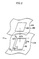
FIG. 2 is an equivalent circuit diagram of a pixel of the LCD shown inFIG. 1 according to an exemplary embodiment of the present invention. -
FIG. 3 shows a relationship between the illuminance and a contrast ratio of an LCD according to an exemplary embodiment of the present invention. -
FIG. 4 and FIG. 5 are graphs illustrating examples of relative gamma curves showing a relationship between gray-scale levels and the luminance of an LCD according to exemplary embodiments of the present invention. -
FIG. 6 is a graph showing a comparison result of the relative gamma curve inFIG. 5 and a compensation gamma curve according to an exemplary embodiment of the present invention. -
FIG. 7 is a flowchart illustrating a driving method of an LCD according to an exemplary embodiment of the present invention. - Hereinafter, exemplary embodiments of the present invention will be described in detail with reference to the accompanying drawings In the drawings, the thickness of layers, films, panels and regions may be exaggerated for clarity. Like reference numerals may refer to the same or similar elements throughout the description of the figures. It will be understood that when an element such as a layer, film, region, substrate, or panel is referred to as being "on" another element, it can be directly on the other element or intervening elements may also be present.
- First, an LCD according to an exemplary embodiment of the present invention will be described in detail below with reference to
FIGS. 1 and2 . -
FIG. 1 is a block diagram illustrating an LCD according to an exemplary embodiment of the present invention.FIG. 2 is an equivalent circuit diagram of a pixel of the LCD shown inFIG. 1 according to an exemplary embodiment of the present invention. - Referring to
FIG. 1 , an LCD includes a liquid crystal (LC)panel assembly 300, agate driver 400, adata driver 500, agray voltage generator 800 coupled with thedata driver 500, aphoto sensor 700, and asignal controller 600, Thegate driver 400 and thedata driver 500 are coupled with theLC panel assembly 300, and thesignal controller 600 controls the above-mentioned components, - The
LC panel assembly 300 includes a plurality of signal lines G1-Gn and D1-Dm and a plurality of pixels PX connected to the signal lines G1-Gn and D1-Dm and arranged substantially in a matrix. As shown inFIG. 2 , theLC panel assembly 300 includes alower panel 100 and anupper panel 200 positioned in a plane substantially parallel to the plane of thelower panel 100, and an LC layer 3 interposed therebetween. - The signal lines include a plurality of gate lines G1-Gn for transmitting gate signals (also referred to herein as "scanning signals") and a plurality of data lines D1-Dm for transmitting data voltages. The gate lines G1-Gn extend in a first direction, for example, a row direction and substantially parallel to each other, and the data lines D1-Dm extend in a second direction, for example, a column direction and substantially parallel to each other. The first direction and the second direction are substantially perpendicular to each other.
- In exemplary embodiment of the present invention, each pixel PX, for example, a pixel PX connected to the i-th gate line Gi (i=1, 2, ..., n) and the j-th data line Dj (j=1, 2, ..., m), includes a switching element Q connected to the signal lines Gi and Dj, an LC capacitor Clc connected to the switching element Q, and an optional storage capacitor Cst connected to the switching element Q. The optional storage capacitor Cst may be omitted.
- As shown in
FIG. 2 , the switching element Q is a three-terminal element, and is disposed on thelower panel 100. A control terminal of the switching element Q is connected to the gate line Gi, an input terminal thereof is connected to the data line Dj, and an output terminal thereof is connected to the LC capacitor Clc and the optional storage capacitor Cst. - The LC capacitor Clc uses a
pixel electrode 191 disposed on thelower panel 100 and acommon electrode 270 disposed on theupper panel 200 as its two terminals. The LC layer 3 interposed between the twoelectrodes pixel electrode 191 is connected to the switching element Q. Thecommon electrode 270 is supplied with a common voltage Vcom and is formed on the entire surface of theupper panel 200. Although not shown as such inFIG. 2 , thecommon electrode 270 may be provided on thelower panel 100. At least one of theelectrodes - The storage capacitor Cst may serve as an auxiliary capacitor for the LC capacitor Clc. In the storage capacitor Cst, the
pixel electrode 191 and a separate signal line provided on thelower panel 100 may be overlapped with an insulator therebetween. A predetermined voltage, such as the common voltage Vcom, is applied to the separate signal line. - In the storage capacitor Cst, the
pixel electrode 191 and an adjacent gate line (also called a previous gate line) may be overlapped with an insulator therebetween. - For color display, each pixel PX may uniquely display one of the primary colors (i.e., spatial division) or each pixel PX may sequentially represent the primary colors in turn (i.e., temporal division) so that a desired color is recognized through a spatial and/or temporal sum of the primary colors. The primary colors may be, for example, red, green, and blue.
FIG. 2 shows an example of spatial division, in which each pixel PX includes acolor filter 230 for displaying one of the primary colors in a region of theupper panel 200 corresponding to thepixel electrode 191. Although not shown as such inFIG. 2 , thecolor filter 230 may be provided above or below thepixel electrode 191 of thelower panel 100. - One or more polarizers (not shown) for polarizing light are attached to the
LC panel assembly 300. - Referring back to
FIG. 1 , thegray voltage generator 800 generates gray voltages related to the transmittance of the pixels PX. For example, thegray voltage generator 800 may generate a first number of gray voltages or a second number of gray voltages (also referred to herein as "reference gray voltages"). Some of the (reference) gray voltages have a positive polarity relative to the common voltage Vcom, while the other (reference) gray voltages have a negative polarity relative to the common voltage Vcom, - The
gate driver 400 is connected to the gate lines G1-Gn of theLC panel assembly 300 and applies the gate signals, which comprise a gate-on voltage Von and a gate-off voltage Voff, to the gate lines G1-Gn. - The
data driver 500 is connected to the data lines D1-Dm of theLC panel assembly 300. Thedata driver 500 selects a gray voltage for each data line D1-Dm from thegray voltage generator 800 and applies the selected gray voltages to the data lines D1-Dm. However, when thegray voltage generator 800 generates only a predetermined number of the reference gray voltages instead of voltages corresponding to all gray scales, thedata driver 500 may divide the reference gray voltages to generate gray voltages corresponding to all the gray scales and select the data voltages from the generated gray voltages. - The
photo sensor 700 converts illuminance (i.e., ambient light level) information to an electrical signal to transmit it to thesignal controller 600. - The
signal controller 600 controls thegate driver 400, the data driver 500and/or other driving devices, based on the signal from thephoto sensor 700. - Each of driving
devices LC panel assembly 300 in the form of at least one integrated circuit (IC) chip or mounted on a flexible printed circuit (FPC) film such as a tape carrier package (TCP), which may be attached to thepanel assembly 300. One or more of the drivingdevices LC panel assembly 300 along with the signal lines G1-Gn and D1-Dm and the switching elements Q. - The driving
devices devices devices - Operations of an LCD according to an exemplary embodiment of the present invention will now be described.
- The
signal controller 600 is supplied with input image signals R, G, and B and input control signals for controlling the display of the input image signals R, G, and B from an external graphics controller (not shown). The input image signals R, G, and B contain luminance information for each pixel PX. The luminance has a predetermined number of gray-scale levels, such as for example, 1024 (=210), 256 (=28), or 64 (=26). Examples of input control signals may include a vertical synchronization signal Vsync, a horizontal synchronization signal Hsync, a main clock signal MCLK, a data enable signal DE, and the like. - On the basis of the input control signals and the input image signals R, G, and B, the
signal controller 600 generates a gate control signal CONT1 and a data control signal CONT2. Thesignal controller 600 processes the image signals R, G, and B in such a way to be suitable for the operating conditions of theLC panel assembly 300 and thedata driver 500 based on the input image signals R, G, and B and the input control signals. Thesignal controller 600 outputs the gate control signal CONT1 to thegate driver 400 and outputs the processed image signals DAT and the data control signal CONT2 to thedata driver 500. - The gate control signalsCONT1 may include a scanning start signal (STV) for instructing to start scanning, and at least one clock signal for controlling the output period of the gate-on voltage Von. The gate control signals CONT1 may further include an output enable signal (OE) for defining the duration of the gate-on voltage Von.
- The data control signal CONT2 may include a horizontal synchronization start signal (STH) for informing of start of data transmission for a row of pixels PX, a load signal (LOAD) for instructing to apply the data voltages to the data lines D1-Dm, and a data clock signal (HCLK). The data control signal CONT2 may further include an inversion signal (RVS) for reversing the polarity of the data voltages (relative to the common voltage Vcom).
- Responsive to the data control signal CONT2 from the
signal controller 600, thedata driver 500 receives a packet of the digital image signals DAT for the row of pixels PX from thesignal controller 600, converts the digital image signals DAT into analog data voltages selected from the gray voltages, and applies the analog data voltages to the data lines D1-Dm, - The
gate driver 400 applies the gate-on voltage Von to the gate lines G1-Gn in response to the gate control signal CONT1 from thesignal controller 600, thereby turning on the switching transistors Q connected to the gate lines G1-Gn. The data voltages applied to the data lines D1-Dm are thus applied to the corresponding pixels PX through the activated switching transistors Q. - A difference between a data voltage and the common voltage Vcom applied to a pixel PX may be represented as a voltage across the LC capacitor Clc of the pixel PX, i.e., a pixel voltage, The LC molecules of the LC layer 3 have different orientations depending on the magnitude of the pixel voltage, and the molecular orientations determine the polarization of light that passes through the LC layer 3. The polarizer(s) converts light polarization to light transmittance such that the pixel PX has a luminance represented by a gray of the data voltage,
- By repeating the above procedure by a unit of 1 horizontal period (which is also referred to as "1H" and is equal to one period of the horizontal synchronization signal Hsync and the data enable signal DE), the gate-on voltage Von is sequentially applied to all gate lines G1-Gn and the data voltages are applied to all the pixels PX to display an image for a frame.
- When the next frame starts after one frame finishes, the inversion signal (RVS) applied to the
data driver 500 may be controlled such that the polarity of the data voltages is reversed with respect to that applied in a previous frame (which is referred to as "frame inversion"). The inversion signal (RVS) may be controlled such that the polarity of the data voltages applied to a data line are periodically reversed during one frame (for example, row inversion and dot inversion), or the polarity of the data voltages in one packet are reversed (for example, column inversion and dot inversion). - Hereinafter, a method and an apparatus for driving the LCD according to an exemplary embodiment of the present invention will be described with reference to
FIGS. 3 through 7 . -
FIG. 3 shows a relationship between the illuminance and a contrast ratio of an LCD according to an exemplary embodiment of the present invention.FIG. 4 and FIG. 5 are graphs illustrating examples of relative gamma curves showing a relationship between gray-scale levels and the luminance of an LCD according to an exemplary embodiment of the present invention.FIG. 6 is a graph showing a comparison result of the relative gamma curve inFIG. 5 and a compensation gamma curve.FIG. 7 is a flowchart illustrating a driving method of an LCD according to an exemplary embodiment of the present invention. - In
FIG. 3 , a horizontal axis represents illuminance, a unit of the horizontal axis is Lux, and a vertical axis represents contrast ratio, The graph shown inFIG. 3 was obtained by measuring relationships between illuminance and contrast ratio with respect to a plurality of LCDs A, B, C, and D, - Referring to
FIG. 3 , as the illuminance IL increases, the contrast ratio Y exponential-functionally decreases, as expressed byEquation 1.
where N and E are constants. For example, avalue satisfying Equation 1 was obtained in the LCD A.
where CRb is a contrast ratio measured in a bright room, and IL represents illuminance (i.e., ambient light level). - As used herein, the term "light room" refers to a space in which some light exists, and the term "dark room" refers to a space in which light is substantially blocked.
- Meanwhile, when the bit number of a data signal of the LCD is 8, the number of gray-scale levels is 256 (=28), and luminance that is represented by the LCD in each of the gray-scale levels can be represented as a graph. The graph is referred to as a gamma curve. For example, in
Equation 1, "illuminance (IL)" may be replaced by a gray level, and an equation for a gamma curve is obtained. In this case, since an exponential portion (E) is usually replaced by a gamma (γ), the curve is called a gamma curve. The gamma curve exponential-functionally increases or decreases according to a value of a gray level. In an LCD of a normally black mode, as a value of the gray level increases, the luminance of the gamma curve exponential-functionally increases. - For example, the value of the gamma (γ) is about 2.2 in some LCDs, and the value of the gamma (γ) is increased to about 2.4 in LCDs for televisions to increase their luminance.
- In an exemplary embodiment of the present invention, the value of gamma (γ) is defined to be about "1". In this case, the gamma curve has a linear shape. Linear analysis of the gamma curve allows for simplifying an algorithm as well as for providing convenience of analysis. Since the value of the gamma (γ) is defined for convenience of analysis, the value of the gamma (γ) may be changed. A gamma curve for which the value of the gamma (γ) is "1" may be referred to as "a relative gamma curve".
- Since the relative gamma curve and a compensation gamma curve are linear functions, as expressed by Equation 3, when a gradient (Gc) and a point on the compensation gamma curve are obtained, an equation for the compensation gamma curve is obtained. Hereinafter, a method for calculating the gradient and a method for calculating a point on the compensation gamma curve will be described.

where Yc is a compensation gamma curve, Gc is a gradient of the compensation gamma curve, and Y1 represents a point intersecting the Y-axis. -
FIGS. 4 and 5 show examples of relative gamma curves Yd and Yb, respectively. A gradient of the relative gamma curve Yd is denoted "Gd", and a gradient of the relative gamma curve Yb is denoted "Gb". In comparing the two relative gamma curves Yd and Yb, the maximum luminance Lmaxb measured in a bright room is slightly larger than the maximum luminance Lmaxd measured in a dark room, but the minimum luminance Lminb measured in the bright room is much larger than the minimum luminance Lmimd measured in the dark room. This result is due to the reflection of ambient light. - The gradient of the relative gamma curve Yb obtained in the bright room is smaller than that of the relative gamma curve Yd obtained in the dark room. The contrast ratio (CR) is a ratio of the maximum luminance (Lmax) and the minimum luminance (Lmin), for example, as expressed by Equation 4.

- When the respective contrast ratios in the dark room and the bright room are obtained, a relative ratio (K) may be defined as Equation 5.

where, CRd is the contrast ratio in the dark room, and CRb is the contrast ratio in the bright room, and the relative ratio (K) is larger than "1". - Since the constants N and E in
Equation 1 may be calculated by varying the ambient illuminance of the LCD A, for example, the contrast ratio CRb in the bright room may be determined using Equation 2. - A gamma curve may be obtained by measuring luminance with respect to each gray level in the dark room, and the gradient Gd of the relative gamma curve Yd in the dark room and the contrast ratio CRd in the dark room may be defined as constants.
- In addition, the relative gamma curve Yb in the bright room may be experimentally calculated by measuring the luminance with respect to each gray level, for example, similar to the contrast ratio CRb in the bright room as expressed by Equation 2.
- By multiplying the gradient Gd of the measured relative gamma curve Yd in the dark room by the relative ratio K, a gradient Gc of the compensation gamma curve is obtained, which can be written as Equation 6.

- Thus, when the gradient Gc of the compensation gamma curve is larger than the gradient Gd of the relative gamma curve Yd measured in the dark room, the gradient Gc of the compensation gamma curve is much larger than the gradient Gb of the relative gamma curve Yb measured in the bright room.
- After the gradient Gc of the compensation gamma curve is obtained, when a point on the compensation gamma curve is obtained, Equation 3 of the compensation curve Yc isobtained, as shown in
FIG. 6 . A point on the compensation gamma curve may be obtained using the average gray AG. - According to an exemplary embodiment of the present invention, the average gray AG of the input data signals R, G, and B is positioned on the relative gamma curve Yb measured in the bright room before the compensation, and the average gray AC and a luminance value corresponding to the average gray AC become a point (e.g., defined by an X-axis value and a Y-axis value) on the compensation gamma curve.
- As shown in
FIG. 6 , the compensation gamma curve has the gradient Gc and is a line passing through a point C1. - Referring to
FIG. 6 , the average gray AG is positioned at the middle of the two relative gamma curves Yb and Yc, and the two curves Yb and Yc finally intersect at the point C1. The gradient Gc of the compensation gamma curve is larger than the gradient Gb of the relative gamma curve Yb measured in the bright room, - In an exemplary embodiment of the present invention, the compensation gamma curve Yc is substantially the same as the result obtained by rotating the relative gamma curve Yb measured in the bright room with respect to the point C1, and a variation width of the luminance increases, and the visibility may increase.
- As shown in
FIG. 6 , since the gradient becomes large, a high gray level and a low gray level represent the maximum luminance Lmaxb and the minimum luminance Lminb in an LCD. The gray levels of less than the average gray AG represent lower luminance and the gray levels larger the average gray AG represent higher luminance. As a result, since the contrast ratio increases, the visibility improves. - Next, a driving method of an LCD according to an exemplary embodiment of the present invention will be described with reference to
FIG. 7 . - The
photo sensor 700 senses illuminance IL of ambient light (step S01) and converts the sensed illuminance to an electrical signal to transmit to thesignal controller 600. For example, a voltage or current is outputted in proportion to or inversely proportionate to the sensed illuminance IL. - The
signal controller 600 determines a contrast ratio CRb, for example, in accordance with Equation 2 (step S02), based on the signal from thephoto sensor 700. - In addition, the
signal controller 600 determines a gradient Gc of a compensation gamma curve, for example, based on Equation 4 and Equation 5 (step S03), and the average gray AG (step S04), to obtain the compensation gamma curve (step S05). - The
signal controller 600 outputs a control signal based on the compensation gamma curve Yc to thegray voltage generator 800, and thegray voltage generator 800 transmits a gray voltage based on the compensation gamma curve Yc to thedata driver 500 to embody the gamma compensation suitable to the outdoor LCD (step S06). Based on the concept of the gamma compensation according to illuminance variation from the outside, the driving method of thesignal controller 600 may be called "adaptive gamma compensation". - Small-sized display devices such as for a mobile phone may use low-reflective optical sheets that have lower reflectivity outdoors than indoors, and thereby the visibility of the small-sized display devices increases. In a driving method of a liquid crystal display according to an exemplary embodiment of the present invention, the visibility may be improved without the use of reflective sheets, and the manufacturing cost may be reduced. It will be appreciated that a driving method of a liquid crystal display according to an exemplary embodiment of the present invention may be used in conjunction with the use of reflective sheets, and the visibility may be further improved.
- Although exemplary embodiments of the present invention have been described detail with reference to the accompanying drawings for the purpose of illustration, it is to be understood that the inventive processes and apparatus should not be construed as limited thereby. It will be apparent to those of ordinary skill in the art that various modifications to the foregoing exemplary embodiments can be made without departing from the scope of the invention as defined by the appended claims, with equivalents of the claims to be included therein.
Claims (20)
- A driving method of a liquid crystal display, comprising:sensing illuminance of ambient light;determining a first contrast ratio based on the sensed illuminance;determining a second contrast ratio and a relative ratio of the second contrast ratio and the first contrast ratio;determining a gradient of a compensation gamma curve using the relative ratio;determining an average gray level of input data signals; anddetermining the compensation gamma curve.
- The driving method of claim 1, wherein the first contrast ratio is substantially equal to the value of 14514*IL-0.8493, where IL is the sensed illuminance.
- The driving method of claim 2, wherein the relative ratio (K) is defined as K = CRd/CRb, where CRd is the second contrast ratio and CRb is the first contrast ratio.
- The driving method of claim 3, wherein the gradient (Gc) of the compensation gamma curve is defined as Gc = K*Gd, where Gd is a gradient of a first relative gamma curve.
- The driving method of claim 4, wherein the second contrast ratio and the gradient of the first relative gamma curve are predetermined.
- The driving method of claim 5, wherein the first relative gamma curve is measured in a space substantially lacking light and has a gamma value of about 1.
- The driving method of claim 6, wherein the relative ratio is larger than 1.
- The driving method of claim 7, wherein the input data signals comprises luminance information with respect to gray levels, and determining the compensation gamma curve uses a luminance value with respect to the average gray level and the gradient of the compensation gamma curve.
- The driving method of claim 8, wherein the compensation gamma curve intersects a second relative gamma curve before a gamma compensation with respect to the liquid crystal display occurs, and the luminance value with respect to the average gray level is obtained by using the second relative gamma curve.
- The driving method of claim 9, wherein the second relative gamma curve is measured in a bright room.
- A driving apparatus of a liquid crystal display, comprising:a photo sensor sensing illuminance of ambient light; anda signal controller connected to the photo sensor and determining a compensation gamma curve based on the sensed illuminance,wherein the signal controller determines a first contrast ratio based on the sensed illuminance, determines a second contrast ratio and a relative ratio of the contrast ratio, and determines the compensation gamma curve using the relative ratio and an average gray level of input data signals.
- The driving apparatus of claim 11, wherein the first contrast ratio is substantially equal to the value of 14514*IL-0.8493, where IL is the sensed illuminance.
- The driving apparatus of claim 12, wherein the relative ratio (K) is defined as K = CRd/CRb, where CRd is second contrast ratio and CRb is the first contrast ratio.
- The driving apparatus of claim 13, wherein the gradient (Gc) of the compensation gamma curve is defined as Gc = K*Gd, where Gd is a gradient of a first relative gamma curve.
- The driving apparatus of claim 14, wherein the second contrast ratio and the gradient of the first relative gamma curve are predetermined.
- The driving apparatus of claim 15, wherein the first relative gamma curve is measured in a space substantially lacking light and has a gamma value of about 1.
- The driving apparatus of claim 16, wherein the relative ratio is larger than 1.
- The driving apparatus of claim 17, wherein the compensation gamma curve intersects a second relative gamma curve before a gamma compensation with respect to the liquid crystal display occurs, and the luminance value with respect to the average gray level is obtained by using the second relative gamma curve.
- The driving apparatus of claim 18, wherein the second relative gamma curve is measured in a bright room.
- The driving apparatus of claim 19, wherein the liquid crystal display comprises:a plurality of pixels;a gray voltage generator, which is connected to the signal controller, to generate a plurality of gray voltages; anda data driver to select a gray voltage corresponding to the input data signals from the gray voltages to transmit the selected gray voltage to the pixels.
Applications Claiming Priority (1)
| Application Number | Priority Date | Filing Date | Title |
|---|---|---|---|
| KR1020070015846A KR101367133B1 (en) | 2007-02-15 | 2007-02-15 | Method and driving apparatus for liquid crystal display |
Publications (3)
| Publication Number | Publication Date |
|---|---|
| EP1959419A2 true EP1959419A2 (en) | 2008-08-20 |
| EP1959419A3 EP1959419A3 (en) | 2010-06-02 |
| EP1959419B1 EP1959419B1 (en) | 2018-07-18 |
Family
ID=39540789
Family Applications (1)
| Application Number | Title | Priority Date | Filing Date |
|---|---|---|---|
| EP08002006.8A Expired - Fee Related EP1959419B1 (en) | 2007-02-15 | 2008-02-04 | Driving method and driving apparatus of liquid crystal display |
Country Status (6)
| Country | Link |
|---|---|
| US (1) | US8823615B2 (en) |
| EP (1) | EP1959419B1 (en) |
| JP (1) | JP5232957B2 (en) |
| KR (1) | KR101367133B1 (en) |
| CN (1) | CN101246675A (en) |
| TW (1) | TWI510091B (en) |
Cited By (3)
| Publication number | Priority date | Publication date | Assignee | Title |
|---|---|---|---|---|
| GB2493931A (en) * | 2011-08-22 | 2013-02-27 | Apical Ltd | Display Device Brightness and Dynamic Range Compression Control |
| US8847935B2 (en) | 2008-11-07 | 2014-09-30 | Sony Corporation | Display device and electronic product having light sensors in plural pixel regions |
| CN114842807A (en) * | 2021-02-01 | 2022-08-02 | 广州视睿电子科技有限公司 | Brightness adjusting method, system, device and storage medium |
Families Citing this family (27)
| Publication number | Priority date | Publication date | Assignee | Title |
|---|---|---|---|---|
| KR101362169B1 (en) * | 2008-09-24 | 2014-02-13 | 엘지디스플레이 주식회사 | Gamma correction system and correction method the same |
| KR101035625B1 (en) | 2009-11-12 | 2011-05-19 | 삼성모바일디스플레이주식회사 | Display device and driving method thereof |
| JP2011118001A (en) * | 2009-11-30 | 2011-06-16 | Fujitsu Ten Ltd | Video display device |
| US20120013583A1 (en) * | 2009-12-11 | 2012-01-19 | Powell John P | Brightness level adjustment of a lighted display device |
| CN101742084B (en) * | 2010-01-29 | 2012-05-30 | 昆山锐芯微电子有限公司 | Contrast ratio enhancement processing method and processing device |
| KR101147419B1 (en) | 2010-05-04 | 2012-05-22 | 삼성모바일디스플레이주식회사 | Display device and establishing method of gamma for the same |
| JP4999975B2 (en) * | 2010-10-06 | 2012-08-15 | 株式会社ナナオ | Screen light calculation device or method thereof |
| TWI436327B (en) | 2011-03-03 | 2014-05-01 | Novatek Microelectronics Corp | Method and apparatus for driving a display device |
| JP5242752B2 (en) * | 2011-09-16 | 2013-07-24 | 株式会社東芝 | Image processing device |
| JP6105925B2 (en) * | 2012-12-27 | 2017-03-29 | 株式会社東芝 | Image processing apparatus and image display apparatus |
| CN103065609B (en) * | 2013-01-23 | 2016-03-30 | 深圳市华星光电技术有限公司 | A kind of method and Gamma compensation system display being carried out to Gamma compensation |
| CN104216546B (en) * | 2013-06-03 | 2017-03-15 | 鸿富锦精密工业(深圳)有限公司 | Touch control display apparatus |
| KR102113178B1 (en) | 2013-09-12 | 2020-05-21 | 삼성디스플레이 주식회사 | Display apparatus and liquid crystal display apparatus |
| KR102105631B1 (en) * | 2013-12-19 | 2020-04-28 | 엘지디스플레이 주식회사 | Display device |
| KR102207464B1 (en) * | 2013-12-30 | 2021-01-27 | 삼성디스플레이 주식회사 | Display apparatus and driving method thereof |
| KR102142624B1 (en) * | 2013-12-30 | 2020-08-10 | 삼성디스플레이 주식회사 | Display device |
| TWI549116B (en) | 2014-01-24 | 2016-09-11 | 宏碁股份有限公司 | Image processing circuit and method thereof |
| CN104810007B (en) * | 2014-01-29 | 2017-06-30 | 宏碁股份有限公司 | Image processing circuit and its method |
| CN104361873B (en) * | 2014-11-18 | 2017-03-15 | 深圳市华星光电技术有限公司 | The method of adjustment of display parameters, device and liquid crystal display systems |
| KR102305951B1 (en) * | 2015-02-17 | 2021-09-28 | 엘지전자 주식회사 | Image display apparatus |
| JP2018155714A (en) * | 2017-03-21 | 2018-10-04 | アズビル株式会社 | Field equipment and degradation diagnostic method |
| CN107274833B (en) * | 2017-07-31 | 2019-07-09 | 京东方科技集团股份有限公司 | Brightness adjusting method, brightness regulating apparatus, display module and display device |
| CN107831945A (en) * | 2017-11-30 | 2018-03-23 | 北京集创北方科技股份有限公司 | Electronic equipment, display system and its integrated control device, safe verification method |
| JP2019220781A (en) * | 2018-06-18 | 2019-12-26 | 日本放送協会 | Video correction apparatus and program of the same |
| CN111916032B (en) * | 2019-05-10 | 2023-06-27 | 京东方科技集团股份有限公司 | Gamma adjustment method and device for display panel |
| JPWO2021131867A1 (en) * | 2019-12-23 | 2021-07-01 | ||
| CN115132150A (en) * | 2021-03-29 | 2022-09-30 | 北京小米移动软件有限公司 | Display screen brightness processing method and device, electronic equipment and storage medium |
Citations (2)
| Publication number | Priority date | Publication date | Assignee | Title |
|---|---|---|---|---|
| US20050123193A1 (en) * | 2003-12-05 | 2005-06-09 | Nokia Corporation | Image adjustment with tone rendering curve |
| EP1624678A1 (en) * | 2004-03-05 | 2006-02-08 | Matsushita Electric Industries Co., Ltd. | Image signal processing method, image signal processing apparatus, and image displaying apparatus |
Family Cites Families (18)
| Publication number | Priority date | Publication date | Assignee | Title |
|---|---|---|---|---|
| JP3804254B2 (en) * | 1998-02-16 | 2006-08-02 | セイコーエプソン株式会社 | LCD projection device |
| JP2000081608A (en) * | 1998-06-29 | 2000-03-21 | Sanyo Electric Co Ltd | Liquid crystal display device with light condensing mechanism |
| JP2001134235A (en) | 1999-11-04 | 2001-05-18 | Matsushita Electric Ind Co Ltd | Liquid crystal display device |
| JP2002152552A (en) * | 2000-11-10 | 2002-05-24 | Mitsubishi Electric Corp | Gamma correction circuit |
| KR100741891B1 (en) | 2000-12-28 | 2007-07-23 | 엘지.필립스 엘시디 주식회사 | Circuit for driving for liquid crystal display device |
| JP4118027B2 (en) * | 2001-02-28 | 2008-07-16 | 株式会社日立製作所 | Liquid crystal display |
| KR100806908B1 (en) | 2001-10-31 | 2008-02-22 | 삼성전자주식회사 | device for driving liquid crystal device |
| KR100861266B1 (en) | 2002-06-29 | 2008-10-01 | 엘지디스플레이 주식회사 | Method and apparatus for correcting color of liquid crystal display |
| KR100555303B1 (en) | 2002-12-11 | 2006-03-03 | 엘지.필립스 엘시디 주식회사 | Apparatus and method of generating gamma voltage |
| EP1573707A1 (en) * | 2002-12-13 | 2005-09-14 | Koninklijke Philips Electronics N.V. | Automatic gamma correction for a matrix display |
| JP2004294767A (en) | 2003-03-27 | 2004-10-21 | Mitsubishi Electric Corp | Image display device |
| JP4271978B2 (en) * | 2003-04-18 | 2009-06-03 | 株式会社日立製作所 | Video display device |
| JP2005181731A (en) | 2003-12-19 | 2005-07-07 | Sharp Corp | Video projection device |
| JP4899321B2 (en) | 2004-03-05 | 2012-03-21 | パナソニック株式会社 | Image signal processing method, image signal processing apparatus, and image display apparatus |
| KR100662980B1 (en) | 2004-07-23 | 2006-12-28 | 삼성에스디아이 주식회사 | Light emitting display |
| KR20060081218A (en) | 2005-01-07 | 2006-07-12 | 엘지전자 주식회사 | Apparatus for adjusting color |
| JP2006285064A (en) | 2005-04-04 | 2006-10-19 | Matsushita Electric Ind Co Ltd | Image display apparatus |
| US7328116B2 (en) * | 2005-05-02 | 2008-02-05 | Xerox Corporation | Visual monitor calibration |
-
2007
- 2007-02-15 KR KR1020070015846A patent/KR101367133B1/en active IP Right Grant
- 2007-10-31 US US11/931,297 patent/US8823615B2/en active Active
- 2007-12-10 TW TW096147058A patent/TWI510091B/en not_active IP Right Cessation
-
2008
- 2008-01-08 JP JP2008001011A patent/JP5232957B2/en active Active
- 2008-02-04 EP EP08002006.8A patent/EP1959419B1/en not_active Expired - Fee Related
- 2008-02-14 CN CNA2008100082491A patent/CN101246675A/en active Pending
Patent Citations (2)
| Publication number | Priority date | Publication date | Assignee | Title |
|---|---|---|---|---|
| US20050123193A1 (en) * | 2003-12-05 | 2005-06-09 | Nokia Corporation | Image adjustment with tone rendering curve |
| EP1624678A1 (en) * | 2004-03-05 | 2006-02-08 | Matsushita Electric Industries Co., Ltd. | Image signal processing method, image signal processing apparatus, and image displaying apparatus |
Cited By (6)
| Publication number | Priority date | Publication date | Assignee | Title |
|---|---|---|---|---|
| US8847935B2 (en) | 2008-11-07 | 2014-09-30 | Sony Corporation | Display device and electronic product having light sensors in plural pixel regions |
| GB2493931A (en) * | 2011-08-22 | 2013-02-27 | Apical Ltd | Display Device Brightness and Dynamic Range Compression Control |
| CN103946917A (en) * | 2011-08-22 | 2014-07-23 | 顶级公司 | Display device control |
| CN103946917B (en) * | 2011-08-22 | 2016-09-07 | 顶级公司 | Display device control method |
| CN114842807A (en) * | 2021-02-01 | 2022-08-02 | 广州视睿电子科技有限公司 | Brightness adjusting method, system, device and storage medium |
| CN114842807B (en) * | 2021-02-01 | 2023-11-17 | 广州视睿电子科技有限公司 | Brightness adjustment method, system, device and storage medium |
Also Published As
| Publication number | Publication date |
|---|---|
| KR101367133B1 (en) | 2014-02-25 |
| CN101246675A (en) | 2008-08-20 |
| JP5232957B2 (en) | 2013-07-10 |
| TWI510091B (en) | 2015-11-21 |
| US20080198151A1 (en) | 2008-08-21 |
| EP1959419A3 (en) | 2010-06-02 |
| KR20080076203A (en) | 2008-08-20 |
| TW200836559A (en) | 2008-09-01 |
| JP2008197635A (en) | 2008-08-28 |
| EP1959419B1 (en) | 2018-07-18 |
| US8823615B2 (en) | 2014-09-02 |
Similar Documents
| Publication | Publication Date | Title |
|---|---|---|
| EP1959419B1 (en) | Driving method and driving apparatus of liquid crystal display | |
| JP4536514B2 (en) | Luminescence and color change correction in flexible displays | |
| US20090244111A1 (en) | Display device and driving apparatus and method thereof | |
| US7924041B2 (en) | Liquid crystal display including sensing unit for compensation driving | |
| US20070030222A1 (en) | Display device and driving method thereof | |
| US20020057247A1 (en) | LCD for speeding initial bend state, driver and method thereof | |
| US20080218463A1 (en) | Display device and method for driving the same | |
| US8610704B2 (en) | Display device and control method of the same | |
| US8294649B2 (en) | Driving device for display device and image signal compensating method therefor | |
| KR20050042812A (en) | Transflective liquid crystal display with reduced flicker | |
| JP3870954B2 (en) | Liquid crystal panel driving method, liquid crystal device and electronic apparatus | |
| US9761193B2 (en) | Liquid crystal display and driving method thereof | |
| TWI424396B (en) | Optically compensated bend (ocb) liquid crystal display and method of operating same | |
| US20070182897A1 (en) | Liquid crystal display | |
| US20060238471A1 (en) | Driving device and driving method for a display | |
| US8674917B2 (en) | Method and system for adjusting gray-scale level of liquid crystal display device | |
| KR101374889B1 (en) | Electronic device having display device and driving method thereof | |
| JP2001159753A (en) | Liquid crystal panel drive method, liquid crystal device and electronic equipment | |
| TWI410917B (en) | Liquid crystal display | |
| KR20070064062A (en) | Repairing system for liquid crystal display | |
| US20070152933A1 (en) | Driving device for liquid crystal display | |
| KR20070081521A (en) | Driving apparatus for liquid crystal display and liquid crystal display including the same | |
| KR20070027378A (en) | Driving apparatus of display device | |
| JP2007057970A (en) | Electro-optical device, driving method and electronic apparatus | |
| KR20070016782A (en) | Liquid crystal display |
Legal Events
| Date | Code | Title | Description |
|---|---|---|---|
| PUAI | Public reference made under article 153(3) epc to a published international application that has entered the european phase |
Free format text: ORIGINAL CODE: 0009012 |
|
| AK | Designated contracting states |
Kind code of ref document: A2 Designated state(s): AT BE BG CH CY CZ DE DK EE ES FI FR GB GR HR HU IE IS IT LI LT LU LV MC MT NL NO PL PT RO SE SI SK TR |
|
| AX | Request for extension of the european patent |
Extension state: AL BA MK RS |
|
| PUAL | Search report despatched |
Free format text: ORIGINAL CODE: 0009013 |
|
| AK | Designated contracting states |
Kind code of ref document: A3 Designated state(s): AT BE BG CH CY CZ DE DK EE ES FI FR GB GR HR HU IE IS IT LI LT LU LV MC MT NL NO PL PT RO SE SI SK TR |
|
| AX | Request for extension of the european patent |
Extension state: AL BA MK RS |
|
| 17P | Request for examination filed |
Effective date: 20101201 |
|
| AKX | Designation fees paid |
Designated state(s): DE FR GB IT NL |
|
| 17Q | First examination report despatched |
Effective date: 20110519 |
|
| RAP1 | Party data changed (applicant data changed or rights of an application transferred) |
Owner name: SAMSUNG ELECTRONICS CO., LTD. |
|
| RAP1 | Party data changed (applicant data changed or rights of an application transferred) |
Owner name: SAMSUNG DISPLAY CO., LTD. |
|
| RAP1 | Party data changed (applicant data changed or rights of an application transferred) |
Owner name: SAMSUNG DISPLAY CO., LTD. |
|
| GRAP | Despatch of communication of intention to grant a patent |
Free format text: ORIGINAL CODE: EPIDOSNIGR1 |
|
| INTG | Intention to grant announced |
Effective date: 20180207 |
|
| GRAS | Grant fee paid |
Free format text: ORIGINAL CODE: EPIDOSNIGR3 |
|
| GRAA | (expected) grant |
Free format text: ORIGINAL CODE: 0009210 |
|
| AK | Designated contracting states |
Kind code of ref document: B1 Designated state(s): DE FR GB IT NL |
|
| REG | Reference to a national code |
Ref country code: GB Ref legal event code: FG4D |
|
| REG | Reference to a national code |
Ref country code: NL Ref legal event code: FP |
|
| REG | Reference to a national code |
Ref country code: DE Ref legal event code: R096 Ref document number: 602008056026 Country of ref document: DE |
|
| REG | Reference to a national code |
Ref country code: DE Ref legal event code: R097 Ref document number: 602008056026 Country of ref document: DE |
|
| PG25 | Lapsed in a contracting state [announced via postgrant information from national office to epo] |
Ref country code: IT Free format text: LAPSE BECAUSE OF FAILURE TO SUBMIT A TRANSLATION OF THE DESCRIPTION OR TO PAY THE FEE WITHIN THE PRESCRIBED TIME-LIMIT Effective date: 20180718 |
|
| PLBE | No opposition filed within time limit |
Free format text: ORIGINAL CODE: 0009261 |
|
| STAA | Information on the status of an ep patent application or granted ep patent |
Free format text: STATUS: NO OPPOSITION FILED WITHIN TIME LIMIT |
|
| 26N | No opposition filed |
Effective date: 20190423 |
|
| PGFP | Annual fee paid to national office [announced via postgrant information from national office to epo] |
Ref country code: DE Payment date: 20200121 Year of fee payment: 13 Ref country code: NL Payment date: 20200121 Year of fee payment: 13 Ref country code: GB Payment date: 20200123 Year of fee payment: 13 |
|
| PGFP | Annual fee paid to national office [announced via postgrant information from national office to epo] |
Ref country code: FR Payment date: 20200123 Year of fee payment: 13 |
|
| REG | Reference to a national code |
Ref country code: DE Ref legal event code: R119 Ref document number: 602008056026 Country of ref document: DE |
|
| GBPC | Gb: european patent ceased through non-payment of renewal fee |
Effective date: 20210204 |
|
| REG | Reference to a national code |
Ref country code: NL Ref legal event code: MM Effective date: 20210301 |
|
| PG25 | Lapsed in a contracting state [announced via postgrant information from national office to epo] |
Ref country code: NL Free format text: LAPSE BECAUSE OF NON-PAYMENT OF DUE FEES Effective date: 20210301 |
|
| PG25 | Lapsed in a contracting state [announced via postgrant information from national office to epo] |
Ref country code: FR Free format text: LAPSE BECAUSE OF NON-PAYMENT OF DUE FEES Effective date: 20210228 Ref country code: GB Free format text: LAPSE BECAUSE OF NON-PAYMENT OF DUE FEES Effective date: 20210204 Ref country code: DE Free format text: LAPSE BECAUSE OF NON-PAYMENT OF DUE FEES Effective date: 20210901 |