EP1958329B1 - Method of producing surface acoustic wave pressure sensors - Google Patents
Method of producing surface acoustic wave pressure sensors Download PDFInfo
- Publication number
- EP1958329B1 EP1958329B1 EP06844757A EP06844757A EP1958329B1 EP 1958329 B1 EP1958329 B1 EP 1958329B1 EP 06844757 A EP06844757 A EP 06844757A EP 06844757 A EP06844757 A EP 06844757A EP 1958329 B1 EP1958329 B1 EP 1958329B1
- Authority
- EP
- European Patent Office
- Prior art keywords
- wafer
- saw
- cover
- cover wafer
- cuts
- Prior art date
- Legal status (The legal status is an assumption and is not a legal conclusion. Google has not performed a legal analysis and makes no representation as to the accuracy of the status listed.)
- Not-in-force
Links
Images


Classifications
-
- G—PHYSICS
- G01—MEASURING; TESTING
- G01L—MEASURING FORCE, STRESS, TORQUE, WORK, MECHANICAL POWER, MECHANICAL EFFICIENCY, OR FLUID PRESSURE
- G01L9/00—Measuring steady of quasi-steady pressure of fluid or fluent solid material by electric or magnetic pressure-sensitive elements; Transmitting or indicating the displacement of mechanical pressure-sensitive elements, used to measure the steady or quasi-steady pressure of a fluid or fluent solid material, by electric or magnetic means
- G01L9/0001—Transmitting or indicating the displacement of elastically deformable gauges by electric, electro-mechanical, magnetic or electro-magnetic means
- G01L9/0008—Transmitting or indicating the displacement of elastically deformable gauges by electric, electro-mechanical, magnetic or electro-magnetic means using vibrations
- G01L9/0022—Transmitting or indicating the displacement of elastically deformable gauges by electric, electro-mechanical, magnetic or electro-magnetic means using vibrations of a piezoelectric element
- G01L9/0025—Transmitting or indicating the displacement of elastically deformable gauges by electric, electro-mechanical, magnetic or electro-magnetic means using vibrations of a piezoelectric element with acoustic surface waves
-
- Y—GENERAL TAGGING OF NEW TECHNOLOGICAL DEVELOPMENTS; GENERAL TAGGING OF CROSS-SECTIONAL TECHNOLOGIES SPANNING OVER SEVERAL SECTIONS OF THE IPC; TECHNICAL SUBJECTS COVERED BY FORMER USPC CROSS-REFERENCE ART COLLECTIONS [XRACs] AND DIGESTS
- Y10—TECHNICAL SUBJECTS COVERED BY FORMER USPC
- Y10T—TECHNICAL SUBJECTS COVERED BY FORMER US CLASSIFICATION
- Y10T29/00—Metal working
- Y10T29/49—Method of mechanical manufacture
- Y10T29/49002—Electrical device making
- Y10T29/49005—Acoustic transducer
-
- Y—GENERAL TAGGING OF NEW TECHNOLOGICAL DEVELOPMENTS; GENERAL TAGGING OF CROSS-SECTIONAL TECHNOLOGIES SPANNING OVER SEVERAL SECTIONS OF THE IPC; TECHNICAL SUBJECTS COVERED BY FORMER USPC CROSS-REFERENCE ART COLLECTIONS [XRACs] AND DIGESTS
- Y10—TECHNICAL SUBJECTS COVERED BY FORMER USPC
- Y10T—TECHNICAL SUBJECTS COVERED BY FORMER US CLASSIFICATION
- Y10T29/00—Metal working
- Y10T29/49—Method of mechanical manufacture
- Y10T29/49002—Electrical device making
- Y10T29/4902—Electromagnet, transformer or inductor
-
- Y—GENERAL TAGGING OF NEW TECHNOLOGICAL DEVELOPMENTS; GENERAL TAGGING OF CROSS-SECTIONAL TECHNOLOGIES SPANNING OVER SEVERAL SECTIONS OF THE IPC; TECHNICAL SUBJECTS COVERED BY FORMER USPC CROSS-REFERENCE ART COLLECTIONS [XRACs] AND DIGESTS
- Y10—TECHNICAL SUBJECTS COVERED BY FORMER USPC
- Y10T—TECHNICAL SUBJECTS COVERED BY FORMER US CLASSIFICATION
- Y10T29/00—Metal working
- Y10T29/49—Method of mechanical manufacture
- Y10T29/49002—Electrical device making
- Y10T29/4902—Electromagnet, transformer or inductor
- Y10T29/4908—Acoustic transducer
Definitions
- the present invention relates generally to SAW (surface acoustic wave) sensors, and more specifically to wafer level packaging of SAW sensors.
- the present invention relates to methods of forming a number of SAW sensors simultaneously.
- SAW devices can be used to measure a variety of strain-related properties such as temperature, stress, acceleration, and other mechanical parameters, via suitably arranged SAW transducers typically employing a deformable piezoelectric material.
- known piezoelectric material include quartz, lithium niobate lithium tantalate, and treated composites bearing a thin film of a material such as zinc oxide.
- SAW sensors may be used in measuring pressure.
- a need remains for improved SAW sensors adapted for measuring pressure, including air pressure within a tire, as well as other applications.
- a need remains for effective, low-cost manufacturing methods of such SAW sensors.
- the present invention provides a method as defined in Claim 1.
- the method may include the features of any one or more of dependent claims 2 to 6.
- the present invention relates to improved SAW sensors adapted for measuring pressure, as well as to effective, low-cost manufacturing methods of such SAW sensors.
- a SAW sensor includes any SAW device, such as a SAW delay line, SAW resonator, and the like, which can be used for sensing a physical or chemical condition.
- An example embodiment of the present invention is found in a method of simultaneously producing a number of SAW sensors.
- a SAW wafer having a number of SAW transducers disposed thereon is provided.
- a cover wafer is also provided, and a protective wall is provided between the SAW wafer and the cover wafer such that an interior portion of the SAW wafer and an interior portion of the cover wafer are protected and sealed against the outside.
- the cover wafer may be disposed over the SAW wafer such that the protective wall surrounds the SAW transducers.
- the protective wall may be a protective glass frit wall and may provide and define, at least in part, a separation between the cover wafer and the SAW wafer. In some instances, the glass wall may bond the SAW wafer to the cover wafer.
- a number of raised contours may also be provided between the cover wafer and the SAW wafer such that at least one of the raised contours surrounds at least one of the SAW transducers when the cover wafer is disposed over and secured relative to the SAW wafer.
- the SAW wafer may be a quartz SAW wafer
- the cover wafer may be a quartz cover wafer, but this is not required in all embodiments.
- a back side of the SAW wafer may be patterned, such as by etching, to form a number of pressure-sensing diaphragms, each corresponding to an individual pressure sensor on the SAW wafer.
- patterning the SAW wafer includes forming a patterned metal layer on the SAW wafer and a protective metal layer on the cover wafer. The protective metal layer and the glass wall may protect the SAW wafer and the cover wafer during etching.
- a subsequent dicing process may include making a first series of cuts through the cover wafer without cutting the SAW wafer.
- a second series of cuts may be made through the cover wafer without cutting the SAW wafer, the second series of cuts being parallel to the first series of cuts.
- a third series of cuts may be made through the cover wafer and the SAW wafer, the third series of cuts being orthogonal to the first series of cuts and the second series of cuts.
- a fourth series of cuts may be made through the cover wafer and the SAW wafer, the fourth series of cuts being orthogonal to the third series of cuts.
- a wall trench may be provided in the cover wafer, and the protective wall may be provided at least partially within the wall trench.
- a number of contour trenches may also be provided in the cover wafer, and the raised contours may be provided at least partially within the contour trenches.
- a quartz stack including a quartz SAW wafer and a quartz cover wafer.
- a number of SAW transducers may be provided on a surface of the quartz SAW wafer.
- a glass frit wall may be provided between the quartz SAW wafer and the quartz cover wafer such that the glass frit wall surrounds the SAW transducers.
- the glass frit wall may secure the quartz SAW wafer to the quartz cover wafer.
- a number of glass contours may also be provided between the quartz SAW wafer and the quartz cover wafer such that at least one of the glass contours surrounds at least one of the SAW transducers. In some instances, at least one of the glass contours is a rectangular glass frit contour, but this is not required.
- the glass frit wall may have a height that defines a spacing between the quartz SAW wafer and the quartz cover wafer.
- the glass frit wall may, in some instances, have a height that is greater than the spacing between the quartz SAW wafer and the quartz cover wafer.
- the quartz cover wafer may include a wall trench, and the glass frit wall may be at least partially disposed within the wall trench.
- the quartz cover wafer may also include a number of contour trenches, in which case, the glass contours can be at least partially disposed within the contour trenches.
- a SAW pressure sensor may be separated from the glass frit bonded wafers by dicing the quartz stack described above.
- the SAW pressure sensor may include a pressure reference chamber that is formed by a portion of the SAW wafer bearing a SAW transducer, a portion of the cover wafer and one of the glass contours.
- the pressure reference chamber may bear a desired reference pressure as a result of the pressure reference chamber being sealed at the desired reference pressure.
- the SAW pressure sensor may include an overpressure stop, but this is not required.
- the cover wafer portion may be smaller than the SAW wafer portion as a result of the dicing process used to separate the SAW pressure sensor from the quartz stack.
- the SAW pressure sensor may further include conductive leads that are disposed on the SAW wafer portion and that extend outwardly from the SAW transducer beyond the cover wafer portion.
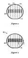
- Figure 1 is a top view of a cover wafer in accordance with an illustrative embodiment of the present invention
- Figure 2 is a top view of a stack incorporating the cover wafer of Figure 1 ;
- Figure 3 is a partial cross-sectional side view taken through Figure 2 at line 3-3;
- Figure 4 is a view of the partial cross-section of Figure 3 , showing a subsequent processing step in accordance with an illustrative embodiment of the present invention
- Figure 5 is a view of the partial cross-section of Figure 4 , showing a subsequent processing step in accordance with an illustrative embodiment of the present invention
- Figure 6 is a partial top view of the stack of Figure 2 , showing a dicing pattern
- Figure 7 is a partial cross-section of the stack of Figure 6 ;
- Figure 8 is a cross-sectional side view of a SAW sensor formed by the dicing pattern shown in Figures 6 and 7 ;
- Figure 9 is a partial cross-sectional side view of a cover wafer in accordance with an illustrative embodiment of the present invention.
- Figure 10 is a view of the partial cross-section of Figure 9 , showing a subsequent processing step in accordance with an illustrative embodiment of the invention.
- Figure 11 is a cross-sectional view of a SAW sensor formed in accordance with an illustrative embodiment of the present invention.
- FIG 1 is a top view of an illustrative cover wafer 10.
- cover wafer 10 may include or be formed from quartz, but this is not required.
- the illustrative cover wafer 10 has a top surface 12 bearing several structures of interest.
- a protective wall such as a glass wall 14, may be positioned on the top surface 12, proximate a periphery 16 of the cover wafer 10.
- glass wall 14 may be disposed about 1 or 2 millimeters inward from periphery 16 of the cover wafer 10. However, it is contemplated that the glass wall 14 may be spaced inward any suitable distance from the periphery 16 of the cover wafer 10.
- Glass wall 14 may be formed having any suitable dimensions.
- glass wall 14 may be about 2 or 3 millimeters in width (parallel to top surface 12) and about 15 to 75 micrometers in height (orthogonal to top surface 12).
- glass wall 14 may be a glass frit wall, formed using known glass frit techniques such as screen printing.
- a number of raised contours 18 may also be provided on surface 12.
- the raised contours 18 may be glass frit contours formed using known glass frit techniques such as screen printing, but this is not required.
- the illustrated embodiment of Figure 1 shows a total of twenty four raised contours 18 disposed on surface 12. It should be noted, however, that surface 12 may include fewer or more raised contours 18, as desired. In some instances, surface 12 may include many more raised contours 18, sometimes evenly disposed about most of surface 12. At least some of the raised contours 18 may be dimensioned to surround a SAW transducer when the cover wafer 10 is disposed over and secured to a SAW wafer. In some instances, raised contours 18 may have a largely rectangular shape, and may be dimensioned to accommodate the particular SAW transducer or transducers used, but this is not required.
- FIG 2 shows an illustrative stack 20 in which cover wafer 10 has been inverted and disposed over a SAW wafer 22, as better seen in Figure 3 .
- Cover wafer 10 may be secured to SAW wafer 22 using any suitable technique.
- cover wafer 10 may be secured to SAW wafer 22 using a thermal annealing process, which may be performed at a temperature of about 450 degrees C.
- SAW wafer 22 may be a quartz wafer.
- SAW transducers 24 may be disposed on SAW wafer 22.
- the SAW transducers 24 do not appear in detail in Figures 2 and 3 , as these are cross-sections.
- SAW transducers 24 may be formed upon SAW wafer 22 using any suitable technique such as a metallization process.
- SAW transducers 24 may be inter-digitized SAW transducers. It should be noted that the wafer-level packaging described herein may be applicable to sealing other quartz devices as well.
- raised contours 18 may be dimensioned to surround SAW transduces 24, while permitting related circuitry and/or conductive leads 25 (shown schematically in Figures 3-5 ) to extend beyond raised contours 18.
- Circuitry and/or conductive leads 25 is best described with respect to Figure 6 .
- circuitry and/or conductive leads 25 can be seen as including several conductive leads ending with conductive pads 27. While the illustrative embodiment shows three conductive leads ending with three conductive pads 27 extending from either side of each SAW transducer 24, it will be appreciated that in some cases, only two leads ending with conductive pads 27 or less, or perhaps four or more leads ending with conductive pads 27, may extend from each SAW transducer 24, as desired.
- FIG. 3 also shows that glass wall 14, in the illustrated embodiment, defines a separation between cover wafer 10 and SAW wafer 22. This separation, as will be discussed subsequently, may in some cases provide advantages during dicing steps. Moreover, as will be discussed, this separation may help define a relatively large pressure reference chamber 26, when desired.
- a pressure sensing diaphragm by deep wet etching of the quartz on the back side of the quartz wafer 22.
- One way to accomplish this, and as shown in Figure 4 includes forming a front side protective masking layer 28 and a back side masking layer 30.
- Layer 28 and layer 30 may be formed of any suitable material using any suitable techniques.
- layer 28 and layer 30 may both be metallic layers such as a Cr/Au layer deposited using techniques such as sputtering, vapor deposition, and the like.
- back side masking layer 30 has been patterned. This patterning may be accomplished using any suitable technique such as a photolithographic process. In some instances, it may be useful to employ a double side aligner so that the future pressure diaphragm is correctly aligned with respect to the corresponding SAW transducer 24.
- glass wall 14 may help protect SAW transducers 24 from damage that may otherwise result from the deep etching process. While a portion of glass wall 14 may be etched away by the etchant, glass wall 14 may have sufficient width to largely withstand the etching process. If there is a high etch rate of the glass wall with respect to the quartz etching, a local laser densification treatment may be performed on glass wall 14 to decrease the etching rate. Once the etching step has occurred, front side protective masking layer 28 and back side masking layer 30 may be removed using any suitable technique.
- Figures 6 and 7 show, in combination, an illustrative dicing or cutting pattern for cutting stack 20 to form a number of individual SAW pressure sensors.
- cover wafer 10 may be cut along the direction TR1. As can be seen in Figure 7 , this cutting may penetrate completely through cover wafer 10 but not contact SAW wafer 22.
- cover wafer 10 may be cut along the direction TR2, which in the illustrative embodiment, is parallel to direction TR1. Once again, this cutting step may penetrate completely through cover wafer 10 but not contact SAW wafer 22.
- a series of cuts may be made along direction TR3, which in the illustrative embodiment, may be perpendicular to directions TR1 and TR2. This cutting step may penetrate completely through both cover wafer 10 and SAW wafer 22.
- a series of cuts may be made along direction TR4, which in the illustrative embodiment, are perpendicular to direction TR3 and thus parallel to directions TR1 and TR2.
- stack 20 may be reduced to a number of individual SAW pressure sensors 34, as shown in Figure 8 .
- FIG 8 shows an illustrative SAW pressure sensor 34 having a cover 36, corresponding to a portion of cover wafer 10 ( Figure 7 ), and a base 38 that corresponds to a portion of SAW wafer 22 ( Figure 7 ). It can be seen that cover 36, base 38 and raised contours 18 may define a pressure reference chamber 26. Base 38 may include a pressure sensing diaphragm 40, formed by the deep etching step discussed previously. SAW pressure sensor 34 may subsequently be provided within a housing or package using, for example, standard plastic encapsulation technology, if desired.
- Figures 9 and 10 show an illustrative cover wafer 42 in accordance with another illustrative embodiment of the present invention.
- the spacing determined by the height of glass wall 14 can provide SAW pressure sensor 34 with a relatively large pressure reference chamber 26.
- variations in chamber volume caused by movement of diaphragm 40 may be relatively small, thereby providing a relatively stable and constant reference pressure.
- this large spacing may make it more difficult to provide an overpressure stop for the diaphragm.
- Figure 9 shows a cover wafer 42, which in some instances may be quartz, with a wall trench 44 and a number of contour trenches 46 formed within a surface 48.
- Wall trench 44 and contour trenches 46 may be formed using any suitable technique, such as depositing and patterning a mask layer, followed by deep wet etching.
- a glass material 50 is disposed at least partially within wall trench 44 while a number of raised contours 52 are disposed at least partially within contour trenches 46.
- Glass material 50 may, in some instances, be a glass frit wall, formed using known glass frit techniques such as screen printing.
- raised contours 52 may be formed using known glass frit techniques such as screen printing, but this is not required in all embodiments.
- cover wafer 42 may be used in place of cover wafer 10 ( Figure 1 ).
- the resulting stack may be processed as discussed with respect to Figures 4 through 7 , and may result in a SAW pressure sensor 54 ( Figure 11 ) having a smaller pressure reference chamber 26.
- SAW pressure sensor 54 has a top 56 corresponding to an appropriate portion of cover wafer 42.
- a base 58 includes a pressure sensing diaphragm 60 and a SAW transducer 24 (as shown in Figure 6 ).
- SAW pressure sensor 54 may be considered as including an overpressure stop, as pressure sensor diaphragm 60 can, if subjected to a sufficiently large pressure differential, actually move far enough to physically contact top 52.
- top 52 functions as an overpressure stop as it may limit physical movement of pressure sensor diaphragm 60.
Landscapes
- Physics & Mathematics (AREA)
- Acoustics & Sound (AREA)
- General Physics & Mathematics (AREA)
- Measuring Fluid Pressure (AREA)
- Pressure Sensors (AREA)
Abstract
Description
- The present invention relates generally to SAW (surface acoustic wave) sensors, and more specifically to wafer level packaging of SAW sensors. In particular, the present invention relates to methods of forming a number of SAW sensors simultaneously.
- SAW devices can be used to measure a variety of strain-related properties such as temperature, stress, acceleration, and other mechanical parameters, via suitably arranged SAW transducers typically employing a deformable piezoelectric material. Examples of known piezoelectric material include quartz, lithium niobate lithium tantalate, and treated composites bearing a thin film of a material such as zinc oxide.
- In some instances, SAW sensors may be used in measuring pressure. A need remains for improved SAW sensors adapted for measuring pressure, including air pressure within a tire, as well as other applications. A need remains for effective, low-cost manufacturing methods of such SAW sensors.
-
DE 10 2004 004476 B3 - The present invention provides a method as defined in Claim 1.
- The method may include the features of any one or more of dependent claims 2 to 6.
- The present invention relates to improved SAW sensors adapted for measuring pressure, as well as to effective, low-cost manufacturing methods of such SAW sensors. A SAW sensor includes any SAW device, such as a SAW delay line, SAW resonator, and the like, which can be used for sensing a physical or chemical condition.
- An example embodiment of the present invention is found in a method of simultaneously producing a number of SAW sensors. In the example method, a SAW wafer having a number of SAW transducers disposed thereon is provided. A cover wafer is also provided, and a protective wall is provided between the SAW wafer and the cover wafer such that an interior portion of the SAW wafer and an interior portion of the cover wafer are protected and sealed against the outside. The cover wafer may be disposed over the SAW wafer such that the protective wall surrounds the SAW transducers. In some cases, the protective wall may be a protective glass frit wall and may provide and define, at least in part, a separation between the cover wafer and the SAW wafer. In some instances, the glass wall may bond the SAW wafer to the cover wafer.
- In some instances, a number of raised contours may also be provided between the cover wafer and the SAW wafer such that at least one of the raised contours surrounds at least one of the SAW transducers when the cover wafer is disposed over and secured relative to the SAW wafer. In some cases, the SAW wafer may be a quartz SAW wafer, and the cover wafer may be a quartz cover wafer, but this is not required in all embodiments.
- After the cover wafer and SAW wafer are secured together, a back side of the SAW wafer may be patterned, such as by etching, to form a number of pressure-sensing diaphragms, each corresponding to an individual pressure sensor on the SAW wafer. In some instances, patterning the SAW wafer includes forming a patterned metal layer on the SAW wafer and a protective metal layer on the cover wafer. The protective metal layer and the glass wall may protect the SAW wafer and the cover wafer during etching.
- A subsequent dicing process may include making a first series of cuts through the cover wafer without cutting the SAW wafer. A second series of cuts may be made through the cover wafer without cutting the SAW wafer, the second series of cuts being parallel to the first series of cuts. A third series of cuts may be made through the cover wafer and the SAW wafer, the third series of cuts being orthogonal to the first series of cuts and the second series of cuts. A fourth series of cuts may be made through the cover wafer and the SAW wafer, the fourth series of cuts being orthogonal to the third series of cuts.
- In some cases, a wall trench may be provided in the cover wafer, and the protective wall may be provided at least partially within the wall trench. In some cases, a number of contour trenches may also be provided in the cover wafer, and the raised contours may be provided at least partially within the contour trenches.
- Another example useful for the understanding of the present invention may be found in a quartz stack including a quartz SAW wafer and a quartz cover wafer. A number of SAW transducers may be provided on a surface of the quartz SAW wafer. A glass frit wall may be provided between the quartz SAW wafer and the quartz cover wafer such that the glass frit wall surrounds the SAW transducers. The glass frit wall may secure the quartz SAW wafer to the quartz cover wafer. A number of glass contours may also be provided between the quartz SAW wafer and the quartz cover wafer such that at least one of the glass contours surrounds at least one of the SAW transducers. In some instances, at least one of the glass contours is a rectangular glass frit contour, but this is not required.
- The glass frit wall may have a height that defines a spacing between the quartz SAW wafer and the quartz cover wafer. Alternatively, the glass frit wall may, in some instances, have a height that is greater than the spacing between the quartz SAW wafer and the quartz cover wafer. In such cases, the quartz cover wafer may include a wall trench, and the glass frit wall may be at least partially disposed within the wall trench. The quartz cover wafer may also include a number of contour trenches, in which case, the glass contours can be at least partially disposed within the contour trenches.
- A SAW pressure sensor may be separated from the glass frit bonded wafers by dicing the quartz stack described above. The SAW pressure sensor may include a pressure reference chamber that is formed by a portion of the SAW wafer bearing a SAW transducer, a portion of the cover wafer and one of the glass contours. The pressure reference chamber may bear a desired reference pressure as a result of the pressure reference chamber being sealed at the desired reference pressure. In some instances, the SAW pressure sensor may include an overpressure stop, but this is not required.
- In some instances, the cover wafer portion may be smaller than the SAW wafer portion as a result of the dicing process used to separate the SAW pressure sensor from the quartz stack. The SAW pressure sensor may further include conductive leads that are disposed on the SAW wafer portion and that extend outwardly from the SAW transducer beyond the cover wafer portion.
- The above summary of the present invention is not intended to describe each disclosed embodiment or every.implementation of the present invention. The Figures, Detailed Description and Examples which follow more particularly exemplify these embodiments.
- The invention may be more completely understood in consideration of the following detailed description of various embodiments of the invention in connection with the accompanying drawings, in which:
-
Figure 1 is a top view of a cover wafer in accordance with an illustrative embodiment of the present invention; -
Figure 2 is a top view of a stack incorporating the cover wafer ofFigure 1 ; -
Figure 3 is a partial cross-sectional side view taken throughFigure 2 at line 3-3; -
Figure 4 is a view of the partial cross-section ofFigure 3 , showing a subsequent processing step in accordance with an illustrative embodiment of the present invention; -
Figure 5 is a view of the partial cross-section ofFigure 4 , showing a subsequent processing step in accordance with an illustrative embodiment of the present invention; -
Figure 6 is a partial top view of the stack ofFigure 2 , showing a dicing pattern; -
Figure 7 is a partial cross-section of the stack ofFigure 6 ; -
Figure 8 is a cross-sectional side view of a SAW sensor formed by the dicing pattern shown inFigures 6 and7 ; -
Figure 9 is a partial cross-sectional side view of a cover wafer in accordance with an illustrative embodiment of the present invention; -
Figure 10 is a view of the partial cross-section ofFigure 9 , showing a subsequent processing step in accordance with an illustrative embodiment of the invention.; and -
Figure 11 is a cross-sectional view of a SAW sensor formed in accordance with an illustrative embodiment of the present invention. - While the invention is amenable to various modifications and alternative forms, specifics thereof have been shown by way of example in the drawings and will be described in detail. It should be understood, however, that the intention is not to limit the invention to the particular embodiments described. On the contrary, the intention is to cover all modifications, equivalents, and alternatives falling within the spirit and scope of the invention.
- The following description should be read with reference to the drawings, in which like elements in different drawings are numbered in like fashion. The drawings, which are not necessarily to scale, depict selected embodiments and are not intended to limit the scope of the invention. Although examples of construction, dimensions, and materials are illustrated for the various elements, those skilled in the art will recognize that many of the examples provided have suitable alternatives that may be utilized.
-
Figure 1 is a top view of anillustrative cover wafer 10. In some instances,cover wafer 10 may include or be formed from quartz, but this is not required. Theillustrative cover wafer 10 has atop surface 12 bearing several structures of interest. A protective wall such as aglass wall 14, may be positioned on thetop surface 12, proximate aperiphery 16 of thecover wafer 10. In some instances,glass wall 14 may be disposed about 1 or 2 millimeters inward fromperiphery 16 of thecover wafer 10. However, it is contemplated that theglass wall 14 may be spaced inward any suitable distance from theperiphery 16 of thecover wafer 10. -
Glass wall 14 may be formed having any suitable dimensions. For example, and in some cases,glass wall 14 may be about 2 or 3 millimeters in width (parallel to top surface 12) and about 15 to 75 micrometers in height (orthogonal to top surface 12). In some instances,glass wall 14 may be a glass frit wall, formed using known glass frit techniques such as screen printing. - In the illustrative embodiment, a number of raised
contours 18 may also be provided onsurface 12. In some instances, the raisedcontours 18 may be glass frit contours formed using known glass frit techniques such as screen printing, but this is not required. The illustrated embodiment ofFigure 1 shows a total of twenty four raisedcontours 18 disposed onsurface 12. It should be noted, however, thatsurface 12 may include fewer or more raisedcontours 18, as desired. In some instances,surface 12 may include many more raisedcontours 18, sometimes evenly disposed about most ofsurface 12. At least some of the raisedcontours 18 may be dimensioned to surround a SAW transducer when thecover wafer 10 is disposed over and secured to a SAW wafer. In some instances, raisedcontours 18 may have a largely rectangular shape, and may be dimensioned to accommodate the particular SAW transducer or transducers used, but this is not required. -
Figure 2 shows anillustrative stack 20 in which coverwafer 10 has been inverted and disposed over aSAW wafer 22, as better seen inFigure 3 .Cover wafer 10 may be secured toSAW wafer 22 using any suitable technique. For example,cover wafer 10 may be secured toSAW wafer 22 using a thermal annealing process, which may be performed at a temperature of about 450 degrees C. In some instances,SAW wafer 22 may be a quartz wafer. - As best illustrated in
Figure 6 , a number ofSAW transducers 24 may be disposed onSAW wafer 22. The SAW transducers 24 do not appear in detail inFigures 2 and3 , as these are cross-sections.SAW transducers 24 may be formed uponSAW wafer 22 using any suitable technique such as a metallization process.SAW transducers 24 may be inter-digitized SAW transducers. It should be noted that the wafer-level packaging described herein may be applicable to sealing other quartz devices as well. - It can be seen that raised
contours 18 may be dimensioned to surround SAW transduces 24, while permitting related circuitry and/or conductive leads 25 (shown schematically inFigures 3-5 ) to extend beyond raisedcontours 18. Circuitry and/or conductive leads 25 is best described with respect toFigure 6 . InFigure 6 , circuitry and/or conductive leads 25 can be seen as including several conductive leads ending withconductive pads 27. While the illustrative embodiment shows three conductive leads ending with threeconductive pads 27 extending from either side of eachSAW transducer 24, it will be appreciated that in some cases, only two leads ending withconductive pads 27 or less, or perhaps four or more leads ending withconductive pads 27, may extend from eachSAW transducer 24, as desired. - As a result, electrical communication with
SAW transducers 24 may be achieved without impacting sealing aroundSAW transducers 24.Figure 3 also shows thatglass wall 14, in the illustrated embodiment, defines a separation betweencover wafer 10 andSAW wafer 22. This separation, as will be discussed subsequently, may in some cases provide advantages during dicing steps. Moreover, as will be discussed, this separation may help define a relatively largepressure reference chamber 26, when desired. - In order to form a SAW pressure sensor, it may be useful to provide a pressure sensing diaphragm by deep wet etching of the quartz on the back side of the
quartz wafer 22. One way to accomplish this, and as shown inFigure 4 , includes forming a front sideprotective masking layer 28 and a backside masking layer 30.Layer 28 andlayer 30 may be formed of any suitable material using any suitable techniques. In some instances,layer 28 andlayer 30 may both be metallic layers such as a Cr/Au layer deposited using techniques such as sputtering, vapor deposition, and the like. - In
Figure 5 , It can be seen that backside masking layer 30 has been patterned. This patterning may be accomplished using any suitable technique such as a photolithographic process. In some instances, it may be useful to employ a double side aligner so that the future pressure diaphragm is correctly aligned with respect to thecorresponding SAW transducer 24. - Once patterning has been complete, deep wet etching of a portion of the back side of
SAW wafer 22 may be completed. This may result invoids 32 that will eventually form and release the pressure diaphragms. It should be noted that during deep etching,glass wall 14 may help protectSAW transducers 24 from damage that may otherwise result from the deep etching process. While a portion ofglass wall 14 may be etched away by the etchant,glass wall 14 may have sufficient width to largely withstand the etching process. If there is a high etch rate of the glass wall with respect to the quartz etching, a local laser densification treatment may be performed onglass wall 14 to decrease the etching rate. Once the etching step has occurred, front sideprotective masking layer 28 and backside masking layer 30 may be removed using any suitable technique. -
Figures 6 and7 show, in combination, an illustrative dicing or cutting pattern for cuttingstack 20 to form a number of individual SAW pressure sensors. In an initial cutting step,cover wafer 10 may be cut along the direction TR1. As can be seen inFigure 7 , this cutting may penetrate completely throughcover wafer 10 but not contactSAW wafer 22. In a second cutting step,cover wafer 10 may be cut along the direction TR2, which in the illustrative embodiment, is parallel to direction TR1. Once again, this cutting step may penetrate completely throughcover wafer 10 but not contactSAW wafer 22. - Next, a series of cuts may be made along direction TR3, which in the illustrative embodiment, may be perpendicular to directions TR1 and TR2. This cutting step may penetrate completely through both
cover wafer 10 andSAW wafer 22. In a further cutting step, a series of cuts may be made along direction TR4, which in the illustrative embodiment, are perpendicular to direction TR3 and thus parallel to directions TR1 and TR2. As a result of these cutting processes, stack 20 may be reduced to a number of individualSAW pressure sensors 34, as shown inFigure 8 . In some instances, as illustrated it can be noted that as a result of the dicing process, there is no cover above at least a portion of theelectrodes 25 andconductive pads 27, which permits electrical communication between theSAW pressure sensor 34 and external circuitry such as a signal conditioning circuit or an antennae. -
Figure 8 shows an illustrativeSAW pressure sensor 34 having acover 36, corresponding to a portion of cover wafer 10 (Figure 7 ), and a base 38 that corresponds to a portion of SAW wafer 22 (Figure 7 ). It can be seen thatcover 36,base 38 and raisedcontours 18 may define apressure reference chamber 26.Base 38 may include apressure sensing diaphragm 40, formed by the deep etching step discussed previously.SAW pressure sensor 34 may subsequently be provided within a housing or package using, for example, standard plastic encapsulation technology, if desired. -
Figures 9 and10 show anillustrative cover wafer 42 in accordance with another illustrative embodiment of the present invention. As discussed previously, the spacing determined by the height of glass wall 14 (Figure 1 ) can provideSAW pressure sensor 34 with a relatively largepressure reference chamber 26. As a result, variations in chamber volume caused by movement ofdiaphragm 40 may be relatively small, thereby providing a relatively stable and constant reference pressure. However, this large spacing may make it more difficult to provide an overpressure stop for the diaphragm. -
Figure 9 shows acover wafer 42, which in some instances may be quartz, with a wall trench 44 and a number ofcontour trenches 46 formed within asurface 48. Wall trench 44 andcontour trenches 46 may be formed using any suitable technique, such as depositing and patterning a mask layer, followed by deep wet etching. InFigure 10 , aglass material 50 is disposed at least partially within wall trench 44 while a number of raisedcontours 52 are disposed at least partially withincontour trenches 46.Glass material 50 may, in some instances, be a glass frit wall, formed using known glass frit techniques such as screen printing. Similarly, raisedcontours 52 may be formed using known glass frit techniques such as screen printing, but this is not required in all embodiments. - It should be appreciated that
cover wafer 42 may be used in place of cover wafer 10 (Figure 1 ). The resulting stack may be processed as discussed with respect toFigures 4 through 7 , and may result in a SAW pressure sensor 54 (Figure 11 ) having a smallerpressure reference chamber 26. As seen inFigure 11 ,SAW pressure sensor 54 has a top 56 corresponding to an appropriate portion ofcover wafer 42. Abase 58 includes apressure sensing diaphragm 60 and a SAW transducer 24 (as shown inFigure 6 ). -
SAW pressure sensor 54 may be considered as including an overpressure stop, aspressure sensor diaphragm 60 can, if subjected to a sufficiently large pressure differential, actually move far enough to physically contact top 52. In this, top 52 functions as an overpressure stop as it may limit physical movement ofpressure sensor diaphragm 60. - The invention should not be considered limited to the particular examples described above, but rather should be understood to cover all aspects of the invention as set out in the attached claims. Various modifications, equivalent processes, as well as numerous structures to which the invention can be applicable will be readily apparent to those of skill in the art upon review of the instant specification.
Claims (6)
- A method of simultaneously producing a plurality of SAW sensors, the method comprising the steps of:providing a SAW wafer (22), the SAW wafer including a plurality of SAW transducers (24) disposed thereon;providing a cover wafer (10);providing a protective wall (14) proximate a periphery of the cover wafer and inbetween the SAW wafer and the cover wafer;securing the cover wafer relative to the SAW wafer such that the protective wall, the SAW wafer, and cover wafer collectively define a pressure chamber (26) that surrounds the plurality of SAW transducers; andafter securing the cover wafer to the SAW wafer, etching one or more of the SAW wafer and cover wafer with an etchant;wherein the protective wall is configured to prevent the etchant from entering the pressure reference chamber.
- The method of claim 1, wherein the step of providing a protective wall (14) includes providing a glass frit protective wall disposed on the cover wafer.
- The method of claim 1, further comprising a step of providing a plurality of raised contours (18) between the SAW wafer (22) and the cover wafer (10) such that at least one of the plurality of raised contours surrounds at least one of the plurality of SAW transducers (24) when the cover wafer is secured to the SAW wafer.
- The method of claim 1, further comprising a step of patterning the SAW wafer (22) after the cover wafer is secured to the SAW wafer.
- The method of claim 1, wherein the step of etching one or more of the SAW wafer (22) and the cover wafer includes etching a backside of the SAW wafer to form pressure-sensing diaphragms (40) from the SAW wafer.
- The method of claim 1, further comprising a subsequent dicing process comprising the steps of:making a first series of cuts through the cover wafer (10) without cutting the SAW wafer (22);making a second series of cuts through the cover wafer without cutting the SAW wafer, the second series of cuts being parallel to the first series of cuts;making a third series of cuts through the cover wafer and the SAW wafer, the third series of cuts being orthogonal to the first and second series of cuts.making a fourth series of cuts through the cover wafer and the SAW wafer, the fourth series of cuts being orthogonal to the third series of cuts.
Applications Claiming Priority (2)
| Application Number | Priority Date | Filing Date | Title |
|---|---|---|---|
| US11/164,845 US7651879B2 (en) | 2005-12-07 | 2005-12-07 | Surface acoustic wave pressure sensors |
| PCT/US2006/046154 WO2007067453A2 (en) | 2005-12-07 | 2006-12-01 | Surface acoustic wave pressure sensors |
Publications (2)
| Publication Number | Publication Date |
|---|---|
| EP1958329A2 EP1958329A2 (en) | 2008-08-20 |
| EP1958329B1 true EP1958329B1 (en) | 2011-08-24 |
Family
ID=38038663
Family Applications (1)
| Application Number | Title | Priority Date | Filing Date |
|---|---|---|---|
| EP06844757A Not-in-force EP1958329B1 (en) | 2005-12-07 | 2006-12-01 | Method of producing surface acoustic wave pressure sensors |
Country Status (4)
| Country | Link |
|---|---|
| US (1) | US7651879B2 (en) |
| EP (1) | EP1958329B1 (en) |
| CN (1) | CN101336513A (en) |
| WO (1) | WO2007067453A2 (en) |
Families Citing this family (5)
| Publication number | Priority date | Publication date | Assignee | Title |
|---|---|---|---|---|
| US7514841B1 (en) * | 2007-10-18 | 2009-04-07 | Honeywell International Inc. | Glass based packaging and attachment of saw torque sensor |
| US8372674B2 (en) * | 2008-02-01 | 2013-02-12 | Honeywell International Inc. | Method for chemical sensor fabrication and related sensor |
| US7891252B2 (en) * | 2008-02-01 | 2011-02-22 | Honeywell International Inc. | Method for sensor fabrication and related sensor and system |
| US8479590B2 (en) | 2010-11-18 | 2013-07-09 | Honeywell International Inc. | System for monitoring structural assets |
| US11402288B2 (en) * | 2014-04-04 | 2022-08-02 | Robert Bosch Gmbh | Membrane-based sensor having a plurality of spacers extending from a cap layer |
Family Cites Families (32)
| Publication number | Priority date | Publication date | Assignee | Title |
|---|---|---|---|---|
| US4100811A (en) | 1977-03-18 | 1978-07-18 | United Technologies Corporation | Differential surface acoustic wave transducer |
| US4216401A (en) | 1978-12-22 | 1980-08-05 | United Technologies Corporation | Surface acoustic wave (SAW) pressure sensor structure |
| FR2451026A1 (en) | 1979-03-09 | 1980-10-03 | Thomson Csf | SURFACE ELASTIC WAVE PRESSURE SENSOR |
| US4296347A (en) | 1979-09-28 | 1981-10-20 | Texas Instruments Incorporated | Surface acoustic wave sensor |
| US4295102A (en) | 1979-09-28 | 1981-10-13 | Texas Instruments Incorporated | Surface acoustic wave sensor sensing circuits |
| GB2100521B (en) | 1981-05-13 | 1984-09-12 | Plessey Co Plc | Electrical device package |
| US5594979A (en) | 1984-09-13 | 1997-01-21 | Raytheon Company | Method for packaging a surface acoustic wave device |
| JPS6297418A (en) | 1985-10-23 | 1987-05-06 | Clarion Co Ltd | Packaging method for surface acoustic wave device |
| US5091051A (en) | 1986-12-22 | 1992-02-25 | Raytheon Company | Saw device method |
| US5010270A (en) | 1986-12-22 | 1991-04-23 | Raytheon Company | Saw device |
| US5345201A (en) | 1988-06-29 | 1994-09-06 | Raytheon Company | Saw device and method of manufacture |
| US5059848A (en) | 1990-08-20 | 1991-10-22 | The United States Of America As Represented By The Secretary Of The Army | Low-cost saw packaging technique |
| DE69206165T2 (en) | 1991-02-04 | 1996-06-05 | Motorola Inc | Hermetic packaging for frequency selective microelectronic parts. |
| US5237235A (en) | 1991-09-30 | 1993-08-17 | Motorola, Inc. | Surface acoustic wave device package |
| JP3379106B2 (en) * | 1992-04-23 | 2003-02-17 | セイコーエプソン株式会社 | Liquid jet head |
| EP0622897B1 (en) | 1993-04-28 | 2001-03-07 | Matsushita Electric Industrial Co., Ltd. | Surface acoustic wave device and method of manufacturing the same |
| US5729185A (en) | 1996-04-29 | 1998-03-17 | Motorola Inc. | Acoustic wave filter package lid attachment apparatus and method utilizing a novolac epoxy based seal |
| DE19637392A1 (en) | 1996-09-13 | 1998-03-26 | Siemens Ag | Pressure sensor using elements working with surface acoustic waves - SAW elements - |
| DE19806818C1 (en) | 1998-02-18 | 1999-11-04 | Siemens Matsushita Components | Method for producing an electronic component, in particular an SAW component working with acoustic surface waves |
| JP2000114918A (en) | 1998-10-05 | 2000-04-21 | Mitsubishi Electric Corp | Surface acoustic wave device and method of manufacturing the same |
| US6287894B1 (en) | 1999-10-04 | 2001-09-11 | Andersen Laboratories, Inc. | Acoustic device packaged at wafer level |
| US6571638B2 (en) | 2000-06-30 | 2003-06-03 | Sawtek, Inc. | Surface-acoustic-wave pressure sensor and associated methods |
| GB0024813D0 (en) | 2000-10-10 | 2000-11-22 | Transense Technologies Plc | Pressure monitoring device incorporating saw device |
| US6890445B2 (en) * | 2001-12-13 | 2005-05-10 | Agere Systems, Inc. | Process for packaging electronic devices using thin bonding regions |
| DE60312493T2 (en) | 2002-03-21 | 2007-07-12 | Transense Technologies Plc, Bicester | PRESSURE MONITOR WITH SURFACE WAVING DEVICE |
| JP4766831B2 (en) * | 2002-11-26 | 2011-09-07 | 株式会社村田製作所 | Manufacturing method of electronic parts |
| JP2004201285A (en) | 2002-12-06 | 2004-07-15 | Murata Mfg Co Ltd | Method of manufacturing piezoelectric component and piezoelectric component |
| JP3905041B2 (en) * | 2003-01-07 | 2007-04-18 | 株式会社日立製作所 | Electronic device and manufacturing method thereof |
| US6907787B2 (en) * | 2003-04-30 | 2005-06-21 | Honeywell International Inc. | Surface acoustic wave pressure sensor with microstructure sensing elements |
| US6962084B2 (en) | 2003-08-06 | 2005-11-08 | Honeywell International Inc. | Sensor with molded sensor diaphragm cover |
| DE102004004476B3 (en) | 2004-01-28 | 2005-07-07 | Infineon Technologies Ag | Resin cover application to a system wafer, comprises applying a cover to a carrier via a connection layer, and then mechanically removing the carrier and connection layer |
| US6964198B2 (en) | 2004-02-25 | 2005-11-15 | Honeywell International Inc. | Sensor testing system and method |
-
2005
- 2005-12-07 US US11/164,845 patent/US7651879B2/en not_active Expired - Fee Related
-
2006
- 2006-12-01 EP EP06844757A patent/EP1958329B1/en not_active Not-in-force
- 2006-12-01 WO PCT/US2006/046154 patent/WO2007067453A2/en not_active Ceased
- 2006-12-01 CN CNA2006800523135A patent/CN101336513A/en active Pending
Also Published As
| Publication number | Publication date |
|---|---|
| WO2007067453A2 (en) | 2007-06-14 |
| WO2007067453A3 (en) | 2007-08-30 |
| EP1958329A2 (en) | 2008-08-20 |
| US20070126072A1 (en) | 2007-06-07 |
| CN101336513A (en) | 2008-12-31 |
| US7651879B2 (en) | 2010-01-26 |
Similar Documents
| Publication | Publication Date | Title |
|---|---|---|
| EP1997347B1 (en) | Mems device | |
| US8497149B2 (en) | MEMS device | |
| US8316718B2 (en) | MEMS pressure sensor device and method of fabricating same | |
| EP2011132B1 (en) | Capacitive micro- electro- mechanical sensors with single crystal silicon electrodes | |
| US7819015B2 (en) | Silicon carbide piezoresistive pressure transducer and method of fabrication | |
| US7891252B2 (en) | Method for sensor fabrication and related sensor and system | |
| US6093579A (en) | Low pressure sensor with a thin boss and method of manufacture | |
| US20150292973A1 (en) | Humidity resistant sensors and methods of making same | |
| CN113483926B (en) | Explosion field MEMS piezoresistive pressure sensor | |
| US7192819B1 (en) | Semiconductor sensor device using MEMS technology | |
| US7651879B2 (en) | Surface acoustic wave pressure sensors | |
| WO2006125941A1 (en) | Surface acoustic wave ( saw) based pressure sensor | |
| JP2012026956A (en) | Pressure sensor manufacturing method and pressure sensor | |
| JP2011038780A (en) | Semiconductor device and method of manufacturing the same | |
| JP6742483B1 (en) | Semiconductor pressure sensor and manufacturing method thereof | |
| JP6773437B2 (en) | Stress sensor | |
| CN121038582A (en) | A piezoelectric pressure sensor and its fabrication method | |
| GB2455214A (en) | MEMS microphone array |
Legal Events
| Date | Code | Title | Description |
|---|---|---|---|
| PUAI | Public reference made under article 153(3) epc to a published international application that has entered the european phase |
Free format text: ORIGINAL CODE: 0009012 |
|
| 17P | Request for examination filed |
Effective date: 20080605 |
|
| AK | Designated contracting states |
Kind code of ref document: A2 Designated state(s): DE FR GB |
|
| 17Q | First examination report despatched |
Effective date: 20081008 |
|
| DAX | Request for extension of the european patent (deleted) | ||
| RBV | Designated contracting states (corrected) |
Designated state(s): DE FR GB |
|
| GRAP | Despatch of communication of intention to grant a patent |
Free format text: ORIGINAL CODE: EPIDOSNIGR1 |
|
| RTI1 | Title (correction) |
Free format text: METHOD OF PRODUCING SURFACE ACOUSTIC WAVE PRESSURE SENSORS |
|
| GRAS | Grant fee paid |
Free format text: ORIGINAL CODE: EPIDOSNIGR3 |
|
| GRAA | (expected) grant |
Free format text: ORIGINAL CODE: 0009210 |
|
| AK | Designated contracting states |
Kind code of ref document: B1 Designated state(s): DE FR GB |
|
| REG | Reference to a national code |
Ref country code: GB Ref legal event code: FG4D |
|
| REG | Reference to a national code |
Ref country code: DE Ref legal event code: R096 Ref document number: 602006024091 Country of ref document: DE Effective date: 20111027 |
|
| PLBE | No opposition filed within time limit |
Free format text: ORIGINAL CODE: 0009261 |
|
| STAA | Information on the status of an ep patent application or granted ep patent |
Free format text: STATUS: NO OPPOSITION FILED WITHIN TIME LIMIT |
|
| 26N | No opposition filed |
Effective date: 20120525 |
|
| REG | Reference to a national code |
Ref country code: DE Ref legal event code: R097 Ref document number: 602006024091 Country of ref document: DE Effective date: 20120525 |
|
| PGFP | Annual fee paid to national office [announced via postgrant information from national office to epo] |
Ref country code: GB Payment date: 20121128 Year of fee payment: 7 |
|
| PGFP | Annual fee paid to national office [announced via postgrant information from national office to epo] |
Ref country code: FR Payment date: 20121219 Year of fee payment: 7 |
|
| PGFP | Annual fee paid to national office [announced via postgrant information from national office to epo] |
Ref country code: DE Payment date: 20121221 Year of fee payment: 7 |
|
| REG | Reference to a national code |
Ref country code: DE Ref legal event code: R119 Ref document number: 602006024091 Country of ref document: DE |
|
| GBPC | Gb: european patent ceased through non-payment of renewal fee |
Effective date: 20131201 |
|
| REG | Reference to a national code |
Ref country code: DE Ref legal event code: R119 Ref document number: 602006024091 Country of ref document: DE Effective date: 20140701 |
|
| REG | Reference to a national code |
Ref country code: FR Ref legal event code: ST Effective date: 20140829 |
|
| PG25 | Lapsed in a contracting state [announced via postgrant information from national office to epo] |
Ref country code: DE Free format text: LAPSE BECAUSE OF NON-PAYMENT OF DUE FEES Effective date: 20140701 |
|
| PG25 | Lapsed in a contracting state [announced via postgrant information from national office to epo] |
Ref country code: GB Free format text: LAPSE BECAUSE OF NON-PAYMENT OF DUE FEES Effective date: 20131201 Ref country code: FR Free format text: LAPSE BECAUSE OF NON-PAYMENT OF DUE FEES Effective date: 20131231 |