EP1956527A1 - Electronic device manufacturing system and electronic device manufacturing method - Google Patents
Electronic device manufacturing system and electronic device manufacturing method Download PDFInfo
- Publication number
- EP1956527A1 EP1956527A1 EP07124167A EP07124167A EP1956527A1 EP 1956527 A1 EP1956527 A1 EP 1956527A1 EP 07124167 A EP07124167 A EP 07124167A EP 07124167 A EP07124167 A EP 07124167A EP 1956527 A1 EP1956527 A1 EP 1956527A1
- Authority
- EP
- European Patent Office
- Prior art keywords
- base sheet
- circuit chip
- conductor patterns
- electronic device
- device manufacturing
- Prior art date
- Legal status (The legal status is an assumption and is not a legal conclusion. Google has not performed a legal analysis and makes no representation as to the accuracy of the status listed.)
- Granted
Links
Images




Classifications
-
- G—PHYSICS
- G06—COMPUTING OR CALCULATING; COUNTING
- G06K—GRAPHICAL DATA READING; PRESENTATION OF DATA; RECORD CARRIERS; HANDLING RECORD CARRIERS
- G06K19/00—Record carriers for use with machines and with at least a part designed to carry digital markings
- G06K19/06—Record carriers for use with machines and with at least a part designed to carry digital markings characterised by the kind of the digital marking, e.g. shape, nature, code
- G06K19/067—Record carriers with conductive marks, printed circuits or semiconductor circuit elements, e.g. credit or identity cards also with resonating or responding marks without active components
- G06K19/07—Record carriers with conductive marks, printed circuits or semiconductor circuit elements, e.g. credit or identity cards also with resonating or responding marks without active components with integrated circuit chips
-
- G—PHYSICS
- G06—COMPUTING OR CALCULATING; COUNTING
- G06K—GRAPHICAL DATA READING; PRESENTATION OF DATA; RECORD CARRIERS; HANDLING RECORD CARRIERS
- G06K19/00—Record carriers for use with machines and with at least a part designed to carry digital markings
- G06K19/06—Record carriers for use with machines and with at least a part designed to carry digital markings characterised by the kind of the digital marking, e.g. shape, nature, code
- G06K19/067—Record carriers with conductive marks, printed circuits or semiconductor circuit elements, e.g. credit or identity cards also with resonating or responding marks without active components
- G06K19/07—Record carriers with conductive marks, printed circuits or semiconductor circuit elements, e.g. credit or identity cards also with resonating or responding marks without active components with integrated circuit chips
- G06K19/077—Constructional details, e.g. mounting of circuits in the carrier
- G06K19/07749—Constructional details, e.g. mounting of circuits in the carrier the record carrier being capable of non-contact communication, e.g. constructional details of the antenna of a non-contact smart card
-
- G—PHYSICS
- G06—COMPUTING OR CALCULATING; COUNTING
- G06K—GRAPHICAL DATA READING; PRESENTATION OF DATA; RECORD CARRIERS; HANDLING RECORD CARRIERS
- G06K19/00—Record carriers for use with machines and with at least a part designed to carry digital markings
-
- G—PHYSICS
- G06—COMPUTING OR CALCULATING; COUNTING
- G06K—GRAPHICAL DATA READING; PRESENTATION OF DATA; RECORD CARRIERS; HANDLING RECORD CARRIERS
- G06K19/00—Record carriers for use with machines and with at least a part designed to carry digital markings
- G06K19/06—Record carriers for use with machines and with at least a part designed to carry digital markings characterised by the kind of the digital marking, e.g. shape, nature, code
- G06K19/067—Record carriers with conductive marks, printed circuits or semiconductor circuit elements, e.g. credit or identity cards also with resonating or responding marks without active components
- G06K19/07—Record carriers with conductive marks, printed circuits or semiconductor circuit elements, e.g. credit or identity cards also with resonating or responding marks without active components with integrated circuit chips
- G06K19/077—Constructional details, e.g. mounting of circuits in the carrier
-
- G—PHYSICS
- G06—COMPUTING OR CALCULATING; COUNTING
- G06K—GRAPHICAL DATA READING; PRESENTATION OF DATA; RECORD CARRIERS; HANDLING RECORD CARRIERS
- G06K19/00—Record carriers for use with machines and with at least a part designed to carry digital markings
- G06K19/06—Record carriers for use with machines and with at least a part designed to carry digital markings characterised by the kind of the digital marking, e.g. shape, nature, code
- G06K19/067—Record carriers with conductive marks, printed circuits or semiconductor circuit elements, e.g. credit or identity cards also with resonating or responding marks without active components
- G06K19/07—Record carriers with conductive marks, printed circuits or semiconductor circuit elements, e.g. credit or identity cards also with resonating or responding marks without active components with integrated circuit chips
- G06K19/077—Constructional details, e.g. mounting of circuits in the carrier
- G06K19/07718—Constructional details, e.g. mounting of circuits in the carrier the record carrier being manufactured in a continuous process, e.g. using endless rolls
-
- G—PHYSICS
- G06—COMPUTING OR CALCULATING; COUNTING
- G06K—GRAPHICAL DATA READING; PRESENTATION OF DATA; RECORD CARRIERS; HANDLING RECORD CARRIERS
- G06K19/00—Record carriers for use with machines and with at least a part designed to carry digital markings
- G06K19/06—Record carriers for use with machines and with at least a part designed to carry digital markings characterised by the kind of the digital marking, e.g. shape, nature, code
- G06K19/067—Record carriers with conductive marks, printed circuits or semiconductor circuit elements, e.g. credit or identity cards also with resonating or responding marks without active components
- G06K19/07—Record carriers with conductive marks, printed circuits or semiconductor circuit elements, e.g. credit or identity cards also with resonating or responding marks without active components with integrated circuit chips
- G06K19/077—Constructional details, e.g. mounting of circuits in the carrier
- G06K19/07749—Constructional details, e.g. mounting of circuits in the carrier the record carrier being capable of non-contact communication, e.g. constructional details of the antenna of a non-contact smart card
- G06K19/0775—Constructional details, e.g. mounting of circuits in the carrier the record carrier being capable of non-contact communication, e.g. constructional details of the antenna of a non-contact smart card arrangements for connecting the integrated circuit to the antenna
-
- H—ELECTRICITY
- H05—ELECTRIC TECHNIQUES NOT OTHERWISE PROVIDED FOR
- H05K—PRINTED CIRCUITS; CASINGS OR CONSTRUCTIONAL DETAILS OF ELECTRIC APPARATUS; MANUFACTURE OF ASSEMBLAGES OF ELECTRICAL COMPONENTS
- H05K3/00—Apparatus or processes for manufacturing printed circuits
- H05K3/0097—Processing two or more printed circuits simultaneously, e.g. made from a common substrate, or temporarily stacked circuit boards
-
- H—ELECTRICITY
- H10—SEMICONDUCTOR DEVICES; ELECTRIC SOLID-STATE DEVICES NOT OTHERWISE PROVIDED FOR
- H10P—GENERIC PROCESSES OR APPARATUS FOR THE MANUFACTURE OR TREATMENT OF DEVICES COVERED BY CLASS H10
- H10P72/00—Handling or holding of wafers, substrates or devices during manufacture or treatment thereof
- H10P72/04—Apparatus for manufacture or treatment
- H10P72/0446—Apparatus for mounting on conductive members, e.g. leadframes or conductors on insulating substrates
-
- H—ELECTRICITY
- H05—ELECTRIC TECHNIQUES NOT OTHERWISE PROVIDED FOR
- H05K—PRINTED CIRCUITS; CASINGS OR CONSTRUCTIONAL DETAILS OF ELECTRIC APPARATUS; MANUFACTURE OF ASSEMBLAGES OF ELECTRICAL COMPONENTS
- H05K1/00—Printed circuits
- H05K1/02—Details
- H05K1/03—Use of materials for the substrate
- H05K1/0393—Flexible materials
-
- H—ELECTRICITY
- H05—ELECTRIC TECHNIQUES NOT OTHERWISE PROVIDED FOR
- H05K—PRINTED CIRCUITS; CASINGS OR CONSTRUCTIONAL DETAILS OF ELECTRIC APPARATUS; MANUFACTURE OF ASSEMBLAGES OF ELECTRICAL COMPONENTS
- H05K2201/00—Indexing scheme relating to printed circuits covered by H05K1/00
- H05K2201/09—Shape and layout
- H05K2201/09209—Shape and layout details of conductors
- H05K2201/09218—Conductive traces
- H05K2201/09227—Layout details of a plurality of traces, e.g. escape layout for Ball Grid Array [BGA] mounting
-
- H—ELECTRICITY
- H05—ELECTRIC TECHNIQUES NOT OTHERWISE PROVIDED FOR
- H05K—PRINTED CIRCUITS; CASINGS OR CONSTRUCTIONAL DETAILS OF ELECTRIC APPARATUS; MANUFACTURE OF ASSEMBLAGES OF ELECTRICAL COMPONENTS
- H05K2203/00—Indexing scheme relating to apparatus or processes for manufacturing printed circuits covered by H05K3/00
- H05K2203/15—Position of the PCB during processing
- H05K2203/1545—Continuous processing, i.e. involving rolls moving a band-like or solid carrier along a continuous production path
-
- H—ELECTRICITY
- H10—SEMICONDUCTOR DEVICES; ELECTRIC SOLID-STATE DEVICES NOT OTHERWISE PROVIDED FOR
- H10W—GENERIC PACKAGES, INTERCONNECTIONS, CONNECTORS OR OTHER CONSTRUCTIONAL DETAILS OF DEVICES COVERED BY CLASS H10
- H10W72/00—Interconnections or connectors in packages
- H10W72/071—Connecting or disconnecting
- H10W72/0711—Apparatus therefor
- H10W72/07141—Means for applying energy, e.g. ovens or lasers
-
- H—ELECTRICITY
- H10—SEMICONDUCTOR DEVICES; ELECTRIC SOLID-STATE DEVICES NOT OTHERWISE PROVIDED FOR
- H10W—GENERIC PACKAGES, INTERCONNECTIONS, CONNECTORS OR OTHER CONSTRUCTIONAL DETAILS OF DEVICES COVERED BY CLASS H10
- H10W72/00—Interconnections or connectors in packages
- H10W72/071—Connecting or disconnecting
- H10W72/072—Connecting or disconnecting of bump connectors
- H10W72/07251—Connecting or disconnecting of bump connectors characterised by changes in properties of the bump connectors during connecting
-
- H—ELECTRICITY
- H10—SEMICONDUCTOR DEVICES; ELECTRIC SOLID-STATE DEVICES NOT OTHERWISE PROVIDED FOR
- H10W—GENERIC PACKAGES, INTERCONNECTIONS, CONNECTORS OR OTHER CONSTRUCTIONAL DETAILS OF DEVICES COVERED BY CLASS H10
- H10W72/00—Interconnections or connectors in packages
- H10W72/20—Bump connectors, e.g. solder bumps or copper pillars; Dummy bumps; Thermal bumps
-
- Y—GENERAL TAGGING OF NEW TECHNOLOGICAL DEVELOPMENTS; GENERAL TAGGING OF CROSS-SECTIONAL TECHNOLOGIES SPANNING OVER SEVERAL SECTIONS OF THE IPC; TECHNICAL SUBJECTS COVERED BY FORMER USPC CROSS-REFERENCE ART COLLECTIONS [XRACs] AND DIGESTS
- Y10—TECHNICAL SUBJECTS COVERED BY FORMER USPC
- Y10T—TECHNICAL SUBJECTS COVERED BY FORMER US CLASSIFICATION
- Y10T29/00—Metal working
- Y10T29/49—Method of mechanical manufacture
- Y10T29/49002—Electrical device making
- Y10T29/49016—Antenna or wave energy "plumbing" making
Definitions
- the present invention relates to an electronic device manufacturing system and electronic device manufacturing method for manufacturing electronic devices which include a conductor pattern formed on a base and a circuit chip electrically connected to the conductor pattern.
- Electronic devices which include a conductor pattern formed on a base such as a printed circuit board and a circuit chip electrically connected to the conductor pattern have been known widely. Such electronic devices are used to control electronic equipment, being incorporated in the electronic equipment, or used as single units to exchange information with the external equipment. As an example of such electronic devices, there have recently been proposed various types of RFID (Radio_Frequency_IDentification) tags which exchange information on a non-contact basis with external equipment exemplified by a reader-writer.
- RFID Radio_Frequency_IDentification
- RFID tag As a type of RFID tag, there have been proposed devices which have a conductor pattern (hereinafter referred to simply as an antenna) which, being formed on a base sheet made of plastics or paper, functions as an antenna for radio communications and an IC chip which, being electrically connected with the antenna, conducts wireless communications via the antenna (see, for example, Japanese Patent Application Publication Nos. 2000-311226 , 2000-200332 , and 2001-351082 ). Possibly, this type of RFID tag can be used for identification of goods by being attached to the goods and exchanging information about the goods with external equipment.
- an antenna which, being formed on a base sheet made of plastics or paper, functions as an antenna for radio communications and an IC chip which, being electrically connected with the antenna, conducts wireless communications via the antenna
- Fig. 1 shows an example of a RFID tag.
- Part (a) of Fig. 1 shows a top view of an RFID tag 1
- Part (b) of Fig. 1 shows a side view of the RFID tag 1 in a longitudinal direction
- Part (c) of Fig. 1 shows an IC chip 11 which is a component of the RFID tag 1.
- the IC chip 11 uses bumps 11a made of gold or the like as connection terminals
- Part (c) of Fig. 1 shows the bumps 11a upside down compared to Parts (a) and (b) of Fig. 1 to provide a view of a surface on which the bumps 11a are formed.
- the RFID tag 1 shown in Fig. 1 includes an antenna 12 formed on a sheet-type base 13 made of a PET film or the like, and an IC chip 11 electrically connected with the antenna 12 via the bumps 11a and bonded to the base 13 with an adhesive.
- the IC chip 11 of the RFID tag 1 can communicate and exchange information with external equipment via the antenna 12.
- the antenna 12 of the RFID tag 1 has a point-asymmetrical shape with two L-shaped patterns placed on both sides of the IC chip 11.
- the two bumps 11a_1 are connected to ends of long sides of the respective L-shaped patterns of the antenna 12.
- the IC chip 11 is mounted on the antenna 12 in such an orientation that the remaining one bump 11a 2 will be located opposite to a projecting direction of short sides of the L-shaped patterns of the antenna 12. In this way, in the example of Fig. 1 , the IC chip 11 is mounted in an orientation which depends on the projecting direction of the short sides of the L-shaped patterns of the antenna 12 (hereinafter the projecting direction of the short sides will be referred to as orientation of the antenna 12).
- typical RFID tags include those which have a point-asymmetrical antenna and on which an IC chip is mounted according to the orientation of the antenna. Ingenuity such as described below has been exercised in manufacturing RFID tags equipped with such a point-asymmetrical antenna.
- Fig. 2 is a diagram showing an example of a tag manufacturing system which manufactures RFID tags equipped with a point-asymmetrical antenna.
- the RFID tag manufactured in the example in Fig. 2 is the RFID tag 1 shown in Fig. 1 .
- the tag manufacturing system 100 shown in Fig. 2 manufactures multiple units of the RFID tag 1 using a base roll 13a produced by rolling up a long base sheet large enough to place multiple bases 13.
- the tag manufacturing system 100 is equipped with an antenna forming apparatus 110 which performs an antenna forming process (step S101) described below.
- the antenna forming process step S101
- first the base roll 13a is loaded on the antenna forming apparatus 110.
- a pattern forming section 111 of the antenna forming apparatus 110 pulls the base sheet out of the base roll 13a and forms multiple antennas 12 on the base sheet.
- the pattern forming section 111 places the multiple antennas 12 in two rows on the base sheet by aligning orientations of antenna patterns as shown in Fig. 2 .
- the base sheet with the antennas formed by the pattern forming section 111 is wound by a winding section (not shown) to produce an antenna-bearing roll body 13a_1. Consequently, the base sheet with the antennas formed is delivered to a next process in the form of a roll body which is easy to handle.
- the tag manufacturing system 100 is equipped with an IC mounting apparatus 130 which performs an IC chip mounting process (step S103) for mounting an IC chip 11 on each antenna 12 on the base sheet.
- the IC mounting apparatus 130 in turn is equipped with a mounter 131 which mounts the IC chips 11 on the antennas 12.
- the mounter 131 is set to mount the IC chips 11 on the antennas in the same orientation as the antennas 12 formed by the pattern forming section 111. This simplifies system architecture.
- the antenna-bearing roll body 13a_1 produced by the antenna forming apparatus 110 were loaded as it was on the IC mounting apparatus 130, the antenna-bearing roll body 13a_1 would be turned 180 degrees during the loading, and consequently the orientation of the antennas 12 on the base sheet pulled out of the antenna-bearing roll body 13a_1 would be 180 degrees opposite to the orientation of the antennas 12 on which the IC chips 11 could be mounted by the mounter 131.
- the tag manufacturing system 100 is equipped with a rewinder 120 which rewinds the roll body, and after the antenna forming process (step S101), a rewind process (step S102) is performed to rewind the antenna-bearing roll body 13a_1 and thereby obtain an antenna-bearing rewound roll body 13a_2.
- the orientation of the antennas 12 on the base sheet pulled out of the antenna-bearing rewound roll body 13a_2 coincides with the orientation of the antennas 12 on which the IC chips 11 can be mounted by the mounter 131. This makes it possible to mount the IC chips 11 normally in the IC chip mounting process (step S103).
- the tag manufacturing system 100 is equipped with a post-processing apparatus 140 which performs a post-process (step S105) for working up the base sheet on which the IC chips have been mounted into finished RFID tags 1 by sealing, cutting, and the like.
- the post-processing apparatus 140 is set to perform post-processing of the base sheet on which the antennas 12 are arranged in the orientation in which they are formed by the pattern forming section 111.
- the IC mounting apparatus 130 winds the base sheet and thereby obtains an IC-chip-carrying roll body 13a_3 to make it easy to deliver the base sheet on which the IC chips have been mounted to a next process, as in the case of the antenna forming apparatus 110.
- a rewind process (step S104) is performed to rewind the IC-chip-carrying roll body 13a_3 by means of the rewinder 120 and thereby obtain an IC-chip-carrying rewound roll body 13a_4.
- the antennas are arranged in the same orientation when handled by the pattern forming section 111, IC mounting apparatus 130, and post-processing apparatus 140, to simplify system architecture. Furthermore, the base sheet is delivered in the form of a roll body between manufacturing processes for ease of delivery, and the inconsistency arising as a result is eliminated by the rewind process performed by the rewinder 120.
- rewind processes such as described above are troublesome for users and cause operation delays during manufacture of RFID tags 1. Also, an increased number of rewind processes will increase loads on the antennas 12 or IC chips 11 on the base sheet and may cause problems such as separation of IC chips 11 or breakage of antennas 12 and IC chips 11.
- the present invention has been made in view of the above circumstances and provides an electronic device manufacturing system and electronic device manufacturing method which can manufacture electronic devices using a reduced number of rewind processes.
- the present invention provides an electronic device manufacturing system that manufactures electronic devices each of which includes a base, a conductor pattern formed into a point-asymmetrical shape on the base, and a circuit chip electrically connected to the conductor pattern, the electronic device manufacturing system including:
- the "point-symmetrical arrangement” mentioned above may be an arrangement of all the conductor patterns on the base sheet or an arrangement of some of the conductor patterns on the base sheet. Alternatively, multiple “point-symmetrical arrangements” may be formed on the base sheet.
- the conductor pattern forming apparatus produces the roll body to make it easy to deliver the base sheet to a next process, and the roll body is handled as it is by the circuit chip mounting apparatus which undertakes a downstream manufacturing process.
- the roll body is turned 180 degrees when it is delivered from the pattern forming apparatus to the circuit chip mounting apparatus, and the point-symmetrical arrangement remains the same after the turn.
- the base sheet on which the point-symmetrical arrangement is formed does not need the rewind process when it is delivered from the pattern forming apparatus to the circuit chip mounting apparatus.
- the elimination of the need for the rewind process leads to reduction in loads on the conductor patterns. In this way, the electronic device manufacturing system according to the present invention can manufacture electronic devices such as RFID tags using a reduced number of rewind processes.
- the base sheet is delivered from the circuit chip mounting apparatus to the post-processing apparatus also in the form of the roll body for ease of delivery and the base sheet on which the point-symmetrical arrangement is formed does not need the rewind process. Consequently, the preferred form of the electronic device manufacturing system makes it possible to manufacture electronic devices without using any rewind process.
- the total elimination of the need for a rewind process makes it possible to avoid problems such as separation of IC chips or breakage of conductor patterns and IC chips which would be caused by the rewind processes.
- the circuit chip mounting apparatus includes a chip transport section which holds the circuit chips, orients the held circuit chips according to the orientations of the respective conductor patterns, and transports the circuit chips onto the conductor patterns.
- the electronic devices may be RFID tags which conduct wireless communications using the circuit chip with the conductor pattern functioning as a communications antenna.
- This aspect makes it possible to manufacture RFID tags using a reduced number of rewind processes.
- the present invention provides an electronic device manufacturing method for manufacturing electronic devices each of which includes a base, a conductor pattern formed into a point-asymmetrical shape on the base, and a circuit chip electrically connected to the conductor pattern, the electronic device manufacturing method including:
- the electronic device manufacturing method according to the present invention makes it possible to manufacture electronic devices using a reduced number of rewind processes.
- the circuit chip mounting step includes holding the circuit chips, orienting the held circuit chips according to the orientations of the respective conductor patterns, and transporting the circuit chips onto the conductor patterns.
- the electronic devices may be RFID tags which conduct wireless communications using the circuit chip with the conductor pattern functioning as a communications antenna.
- the present invention makes it possible to manufacture the electronic devices using a reduced number of rewind processes.
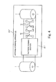
- Fig. 3 is a diagram showing an example of a tag manufacturing system which is an embodiment of the present invention.
- the tag manufacturing system 200 shown in Fig. 3 is an embodiment of the electronic device manufacturing system according to the present invention and a series of processes (described later) performed by the tag manufacturing system 200 is an embodiment of the electronic device manufacturing method according to the present invention.
- the tag manufacturing system 200 manufactures the RFID tag 1 (see Fig. 1 ) equipped with an antenna of a point-asymmetrical shape using a base roll 13a produced by rolling up a long base sheet large enough to place multiple bases 13. It includes an antenna forming apparatus 210, IC mounting apparatus 220, and post-processing apparatus 230.
- the RFID tag 1 manufactured by the tag manufacturing system 200 shown in Fig. 3 is an example of the electronic device according to the present invention and the antenna 12 contained in the RFID tag 1 is an example of the conductor pattern according to the present invention.
- the L-shaped pattern (shown in Fig. 1 ) of the antenna 12 is an example of the point-asymmetrical shape according to the present invention.
- the antenna forming apparatus 210 performs an antenna forming process (step S201) described below and is an example of conductor pattern forming apparatus according to the present invention.
- the antenna forming process (step S201) performed by the antenna forming apparatus 210 is an example of the conductor pattern forming step according to the present invention.
- the antenna forming apparatus 210 includes a pattern forming section 211.
- the pattern forming section 211 pulls the base sheet out of the base roll 13a and forms multiple antennas 12 on the base sheet.
- the pattern forming section 211 has an arrangement rule according to which two antennas 12 are arranged in such a way that long sides of L-shaped patterns extend along the longitudinal direction of the base sheet and that short sides project facing each other as shown in Fig. 3 .
- the pattern forming section 211 forms multiple antennas in a point-symmetrical arrangement according to this arrangement rule.
- the arrangement of the two antennas 12 facing each other is an example of the point-symmetrical arrangement according to the present invention, and an arrangement of multiple pairs of such antennas 12, i.e., the arrangement of all the antennas 12 on the base sheet, is also an example of the point-symmetrical arrangement according to the present invention.
- the base sheet with the antennas formed by the pattern forming section 211 is subsequently wound by a winding section (not shown) to produce an antenna-bearing roll body 13a_5 for ease of delivery of the base sheet.
- the present invention is not limited to this.
- the point-symmetrical arrangement of antennas 12 with L-shaped patterns according to the present invention may be an arrangement such as described below.
- Fig. 4 is a diagram showing another example of the point-symmetrical arrangement.
- Fig. 4 shows another antenna forming apparatus 210' which forms antennas in an arrangement different from the point-symmetrical arrangement shown in Fig. 3 .
- a pattern forming section 211' of the antenna forming apparatus 210' forms two antennas 12 with L-shaped patterns in such a way that the long sides of the L-shaped patterns extend orthogonally to the longitudinal direction of the base sheet and that the short sides project facing each other as shown in Fig. 4 .
- the arrangement of the two antennas 12 shown in Fig. 4 is another example of the point-symmetrical arrangement according to the present invention, and an arrangement of multiple pairs of such antennas 12, i.e., the arrangement of all the antennas 12 on the base sheet, is also an example of the point-symmetrical arrangement according to the present invention.
- the IC mounting apparatus 220 shown in Fig. 3 performs an IC chip mounting process (step S202) to mount IC chips 11 to each antenna 12 on the base sheet.
- the IC mounting apparatus 220 is an example of the circuit chip mounting apparatus according to the present invention.
- the mounting process (step S202) performed by the IC mounting apparatus 220 is an example of the circuit chip mounting step according to the present invention.
- the IC mounting apparatus 220 is equipped with a mounter 221.
- a mounter 2221 When the antenna-bearing roll body 13a 5 is loaded on the IC mounting apparatus 220, first the mounter 221 pulls the base sheet out of the antenna-bearing roll body 13a_5 and mounts an IC chip 11 on each antenna 12 on the base sheet.
- the mounter 221 is equipped with a disposing section (not shown) which disposes IC chip groups arranged in a single orientation and a chip transport section 222 (described below; see Fig. 5 ) which transports the IC chips 11 from the disposing section to the respective antennas 12.
- Fig. 5 is a diagram showing the chip transport section 222.
- the IC chip 11 is mounted on the antenna 12 in such an orientation that the two bumps 11a_1 out of the three bumps 11a are connected to the ends of the long sides of the respective L-shaped patterns of the antenna 12 while the remaining one bump 11a_2 is located opposite to the projecting direction of the short sides of the L-shaped patterns of the antenna 12.
- the antennas 12 placed in a point-symmetrical arrangement differ from each other in the orientation which coincides with the projecting direction of the short sides of the L-shaped patterns as described above, and each of the antennas 12 on the base sheet coincides with one of the two orientations accordingly.
- the chip transport section 222 shown in Fig. 5 has a tip section 222a which, being rotatable in the direction of arrow D in Fig. 5 , holds each IC chip 11, directs the held IC chip 11 in one of the two orientations described above, and transports the IC chip 11 onto the antenna 12 corresponding to the given orientation.
- the chip transport section 222 is an example of the "the chip transport section which holds the circuit chips, orients the held circuit chips according to the orientations of the respective conductor patterns, and transports the circuit chips onto the conductor patterns" according to the present invention.
- IC chip groups are disposed with an orientation corresponding to the orientation of the antennas 12 in the upper of the two rows of antennas 12 in Fig. 5 .
- the chip transport section 222 transports IC chips 11 to the antennas 12 in the upper row, maintaining the orientation in which they are held in the disposing section, i.e., keeping the one bump 11a_2 on the side opposite the projecting direction of the short sides of the antennas 12 in the upper row.
- the chip transport section 222 which holds the IC chips 11 turns the tip section 222a by 180 degrees in the direction of arrow D and thereby orients the IC chips 11 in such a way as to place the tip section 222a on the side opposite the projecting direction of the short sides of the antennas 12 in the lower row.
- the chip transport section 222 turns the tip section 222a appropriately and thereby orients the IC chips 11 according to the orientations of the respective antennas 12 before transporting the IC chips 11. This makes it possible to mount the IC chip 11 on each of multiple antennas 12 in the orientation corresponding to the orientation of the given antenna 12 when the multiple antennas 12 are arranged in two different orientations on the base sheet.
- transport operation of the chip transport section 222 in Fig. 5 including movements of the tip section 222a is specified in advance based on the arrangement rule followed by the pattern forming section 211 during antenna formation.
- the antenna-bearing roll body 13a_5 produced by the antenna forming apparatus 210 is loaded onto the IC mounting apparatus 220 after being turned 180 degrees. In so doing, if the arrangement of the antennas 12 on the base sheet pulled out of the antenna-bearing roll body 13a_5 loaded onto the IC mounting apparatus 220 including the orientations of the antennas 12 do not conform to the arrangement rule, inconsistency can occur during the mounting of the IC chips 11.
- this embodiment since the arrangement of the antennas 12 on the base sheet is point-symmetrical, even if a 180-degree turn is made before loading onto the IC mounting apparatus 220, the arrangements before and after the 180-degree turn coincide, making it possible to avoid the inconsistency described above.
- this embodiment eliminates the need for the rewind process when delivering the antenna-bearing roll body 13a_5 and thereby allows the delivery to be performed smoothly.
- the present invention is not limited to this and the chip mounting apparatus according to the present invention may be equipped with a mounter such as described below.
- Fig. 6 is a diagram showing another example of a mounter.
- the mounter 221' shown in Fig. 6 is equipped with a disposing section 223 in which two wafers with the IC chips 11 formed are disposed.
- a first wafer 223a of the two wafers is disposed in the disposing section 223 in such an orientation that the IC chips 11 can be mounted as they are on one of the two types of antenna 12 facing different directions on the base sheet.
- a second wafer 223b of the two wafers is disposed in the disposing section 223 in such an orientation that the IC chips 11 can be mounted as they are on the other of the two types of antenna 12, i.e., in the orientation opposite to the orientation of the IC chips 11 on the first wafer 223a.
- the disposing section 223 is an example of the disposing section according to the present invention and the first and second wafers 223a and 223b are examples of circuit chip groups according to the present invention.
- the mounter 221' shown in Fig. 6 is equipped with a chip transport section 222' which transports the IC chips 11 on each wafer disposed in the disposing section 223 to the antennas 12 which have the same orientation as the orientation assigned to the given wafer while maintaining the orientation of the IC chips on the wafer.
- the chip transport section 222' is an example of the "chip transport section which transports the circuit chips in each of the multiple circuit chip groups onto the conductor patterns which have the same orientation as the orientation assigned to the given circuit chip group" according to the present invention.
- the first wafer 223a corresponds to the orientation of the upper of the two rows of antennas 12 in the figure while the second wafer 223b corresponds to the orientation of the lower of the two rows of antennas 12 in the figure.
- the chip transport section 222' transports the IC chips 11 on the first wafer 223a to the antennas 12 in the upper row by maintaining the orientation of the IC chips 11 as they are, i.e., keeping the one bump 11a_2 on the side opposite the projecting direction of the short sides of the antennas 12 in the upper row.
- the chip transport section 222' transports the IC chips 11 on the second wafer 223b by maintaining their orientation as they are, i.e., keeping the one bump 11a_2 on the side opposite the projecting direction of the short sides of the antennas 12 in the lower row.
- the chip transport section 222' transports the IC chips 11 from the wafers corresponding to the orientations of the respective antennas 12. Consequently, again the mounter 221' mounts the IC chip 11 on each of multiple antennas 12 in the orientation corresponding to the orientation of the given antenna 12 when the multiple antennas 12 are arranged in two different orientations on the base sheet.
- placement of the wafers in the disposing section 223 and operation of the chip transport section 222' are determined in advance according to the arrangement rule.
- the chip transport section 222' taken as an example of the chip transport section according to the present invention transports the IC chips 11 in the orientation in which they are disposed in the disposing section 223 by transporting them from the disposing section 223 to the antennas
- the chip transport section according to the present invention may be, for example, a type which includes a rotatable arm and a tip section which, being installed at a tip of the arm, holds the IC chips 11, in which the tip section moves between the disposing section 223 and antennas along with rotation of the arm.
- the two wafers are disposed in the disposing section 223 in such a way that the IC chips on the respective wafers are offset by the arm's rotation angle from the orientation in which they can be mounted on the antenna.
- the base sheet with the IC chips mounted is subsequently wound by a winding section (not shown) to produce an IC-chip-carrying roll body 13a_6 for ease of delivery.
- the IC-chip-carrying roll body 13a_6 is turned 180 degrees before delivery and loading onto the post-processing apparatus 230.
- the post-processing apparatus 230 pulls the base sheet on which the IC chips 11 have been mounted on the antennas 12 out of the loaded IC-chip-carryang roll body 13a_6 and performs a post-process (step S203) for working up the base sheet into finished RFID tags 1 by a predetermined sealing process and cutting process.
- the post-processing apparatus 230 is an example of the post-processing apparatus according to the present invention and a series of processes (step S203) performed by the post-processing apparatus 230 is an example of the post-processing step according to the present invention.
- the sealing process is performed for each core section of the RFID tag 1, where the core section is composed of the antenna 12 and IC chip 11.
- the cutting process cuts off the core sections after sealing from each other to obtain multiple RFID tags 1.
- sealing positions on the base sheet, cutting positions on the base sheet, and the like are set in advance according to the arrangement rule.
- the arrangement of the core sections on the base sheet pulled out by the post-processing apparatus 230 including the orientations of the antennas 12 can cause inconsistency during the post-process if it does not conform to the arrangement rule.
- this embodiment since the arrangement of the antennas 12 on the base sheet, and thus the arrangement of core sections, is point-symmetrical, even if the IC-chip-carrying roll body 13a_6 is turned 180 degrees when it is loaded onto the post-processing apparatus 230, the arrangements before and after the 180-degree turn coincide, making it possible to avoid the inconsistency described above.
- this embodiment eliminates the need for the rewind process when delivering the IC-chip-carrying roll body 13a_6 and thereby allows the delivery to be performed smoothly.
- this embodiment totally eliminates the need for a rewind process after all, it can avoid problems such as separation of IC chips 11 or breakage of antennas 12 and IC chips 11 which would be caused by the rewind processes.
- the tag manufacturing system 200 can manufacture RFID tags without using any rewind process.
- the present invention is not limited to this. It is essential for the electronic device manufacturing system according to the present invention only to manufacture electronic devices each of which includes a circuit chip electrically connected to a conductor pattern formed on a base such as a printed circuit board, and for the electronic device manufacturing method according to the present invention only to manufacture the electronic devices.
- the electronic device manufacturing system according to the present invention may manufacture ultrathin IC cards or may manufacture printed circuit board devices with circuit chips fixed to conductor patterns which are formed on a flexible substrate.
- the electronic device manufacturing method according to the present invention may be a method for manufacturing such ultrathin IC cards or printed circuit board devices.
- an L-shaped pattern has been taken as an example of the point-asymmetrical shape in the antenna of the RFID tag according to the present invention
- the present invention is not limited to this.
- the point-asymmetrical shape according to the present invention may be any other pattern shape as long as it is point-asymmetrical.
- the tag manufacturing system 200 illustrated as an embodiment of the electronic device manufacturing system according to the present invention produces the IC-chip-carrying roll body 13a_6 by winding a base sheet on which the IC chips 11 have been mounted and delivers it to an apparatus which performs post-processing
- the present invention is not limited to this.
- the electronic device manufacturing system according to the present invention may perform post-processing of the base sheet immediately without winding the base sheet on which the IC chips 11 have been mounted.
- the post-processing apparatus 230 which performs a sealing process and cutting process has been taken as an example of the post-processing apparatus according to the present invention, the present invention is not limited to this.
- the post-processing apparatus according to the present invention may perform one of the sealing process and cutting process or perform a process other than the sealing process and cutting process.
Landscapes
- Engineering & Computer Science (AREA)
- Microelectronics & Electronic Packaging (AREA)
- Physics & Mathematics (AREA)
- General Physics & Mathematics (AREA)
- Theoretical Computer Science (AREA)
- Computer Hardware Design (AREA)
- Manufacturing & Machinery (AREA)
- Credit Cards Or The Like (AREA)
- Wire Bonding (AREA)
Abstract
Description
- The present invention relates to an electronic device manufacturing system and electronic device manufacturing method for manufacturing electronic devices which include a conductor pattern formed on a base and a circuit chip electrically connected to the conductor pattern.
- Electronic devices which include a conductor pattern formed on a base such as a printed circuit board and a circuit chip electrically connected to the conductor pattern have been known widely. Such electronic devices are used to control electronic equipment, being incorporated in the electronic equipment, or used as single units to exchange information with the external equipment. As an example of such electronic devices, there have recently been proposed various types of RFID (Radio_Frequency_IDentification) tags which exchange information on a non-contact basis with external equipment exemplified by a reader-writer. As a type of RFID tag, there have been proposed devices which have a conductor pattern (hereinafter referred to simply as an antenna) which, being formed on a base sheet made of plastics or paper, functions as an antenna for radio communications and an IC chip which, being electrically connected with the antenna, conducts wireless communications via the antenna (see, for example, Japanese Patent Application Publication Nos.
2000-311226 2000-200332 2001-351082 - Part (a) of
Fig. 1 shows a top view of anRFID tag 1, Part (b) ofFig. 1 shows a side view of theRFID tag 1 in a longitudinal direction, and Part (c) ofFig. 1 shows anIC chip 11 which is a component of theRFID tag 1. Incidentally, theIC chip 11 usesbumps 11a made of gold or the like as connection terminals, and Part (c) ofFig. 1 shows thebumps 11a upside down compared to Parts (a) and (b) ofFig. 1 to provide a view of a surface on which thebumps 11a are formed. - The
RFID tag 1 shown inFig. 1 includes anantenna 12 formed on a sheet-type base 13 made of a PET film or the like, and anIC chip 11 electrically connected with theantenna 12 via thebumps 11a and bonded to thebase 13 with an adhesive. - The
IC chip 11 of theRFID tag 1 can communicate and exchange information with external equipment via theantenna 12. - In the example of
Fig. 1 , theantenna 12 of theRFID tag 1 has a point-asymmetrical shape with two L-shaped patterns placed on both sides of theIC chip 11. In the example ofFig. 1 , out of the threebumps 11a shown in Part (c) ofFig. 1 , the two bumps 11a_1 are connected to ends of long sides of the respective L-shaped patterns of theantenna 12. Furthermore, in the example ofFig. 1 , theIC chip 11 is mounted on theantenna 12 in such an orientation that the remaining onebump 11aantenna 12. In this way, in the example ofFig. 1 , theIC chip 11 is mounted in an orientation which depends on the projecting direction of the short sides of the L-shaped patterns of the antenna 12 (hereinafter the projecting direction of the short sides will be referred to as orientation of the antenna 12). - As shown in
Fig. 1 , typical RFID tags include those which have a point-asymmetrical antenna and on which an IC chip is mounted according to the orientation of the antenna. Ingenuity such as described below has been exercised in manufacturing RFID tags equipped with such a point-asymmetrical antenna. -
Fig. 2 is a diagram showing an example of a tag manufacturing system which manufactures RFID tags equipped with a point-asymmetrical antenna. - Incidentally, the RFID tag manufactured in the example in
Fig. 2 is theRFID tag 1 shown inFig. 1 . - The
tag manufacturing system 100 shown inFig. 2 manufactures multiple units of theRFID tag 1 using abase roll 13a produced by rolling up a long base sheet large enough to placemultiple bases 13. - The
tag manufacturing system 100 is equipped with anantenna forming apparatus 110 which performs an antenna forming process (step S101) described below. In the antenna forming process (step S101), first thebase roll 13a is loaded on theantenna forming apparatus 110. Then, apattern forming section 111 of theantenna forming apparatus 110 pulls the base sheet out of thebase roll 13a and formsmultiple antennas 12 on the base sheet. Thepattern forming section 111 places themultiple antennas 12 in two rows on the base sheet by aligning orientations of antenna patterns as shown inFig. 2 . The base sheet with the antennas formed by thepattern forming section 111 is wound by a winding section (not shown) to produce an antenna-bearing roll body 13a_1. Consequently, the base sheet with the antennas formed is delivered to a next process in the form of a roll body which is easy to handle. - Also, the
tag manufacturing system 100 is equipped with anIC mounting apparatus 130 which performs an IC chip mounting process (step S103) for mounting anIC chip 11 on eachantenna 12 on the base sheet. TheIC mounting apparatus 130 in turn is equipped with amounter 131 which mounts theIC chips 11 on theantennas 12. Themounter 131 is set to mount theIC chips 11 on the antennas in the same orientation as theantennas 12 formed by thepattern forming section 111. This simplifies system architecture. If the antenna-bearing roll body 13a_1 produced by theantenna forming apparatus 110 were loaded as it was on theIC mounting apparatus 130, the antenna-bearing roll body 13a_1 would be turned 180 degrees during the loading, and consequently the orientation of theantennas 12 on the base sheet pulled out of the antenna-bearing roll body 13a_1 would be 180 degrees opposite to the orientation of theantennas 12 on which theIC chips 11 could be mounted by themounter 131. - To eliminate this inconsistency, the
tag manufacturing system 100 is equipped with arewinder 120 which rewinds the roll body, and after the antenna forming process (step S101), a rewind process (step S102) is performed to rewind the antenna-bearing roll body 13a_1 and thereby obtain an antenna-bearing rewound roll body 13a_2. The orientation of theantennas 12 on the base sheet pulled out of the antenna-bearing rewound roll body 13a_2 coincides with the orientation of theantennas 12 on which theIC chips 11 can be mounted by themounter 131. This makes it possible to mount theIC chips 11 normally in the IC chip mounting process (step S103). - Also, the
tag manufacturing system 100 is equipped with apost-processing apparatus 140 which performs a post-process (step S105) for working up the base sheet on which the IC chips have been mounted into finishedRFID tags 1 by sealing, cutting, and the like. To simplify system architecture, as in the case of themounter 131, thepost-processing apparatus 140 is set to perform post-processing of the base sheet on which theantennas 12 are arranged in the orientation in which they are formed by thepattern forming section 111. Then, theIC mounting apparatus 130 winds the base sheet and thereby obtains an IC-chip-carrying roll body 13a_3 to make it easy to deliver the base sheet on which the IC chips have been mounted to a next process, as in the case of theantenna forming apparatus 110. For this reason, after the IC chip mounting process (step S103), a rewind process (step S104) is performed to rewind the IC-chip-carrying roll body 13a_3 by means of therewinder 120 and thereby obtain an IC-chip-carrying rewound roll body 13a_4. - In this way, in the tag manufacturing system shown in
Fig. 2 , the antennas are arranged in the same orientation when handled by thepattern forming section 111,IC mounting apparatus 130, andpost-processing apparatus 140, to simplify system architecture. Furthermore, the base sheet is delivered in the form of a roll body between manufacturing processes for ease of delivery, and the inconsistency arising as a result is eliminated by the rewind process performed by therewinder 120. - However, rewind processes such as described above are troublesome for users and cause operation delays during manufacture of
RFID tags 1. Also, an increased number of rewind processes will increase loads on theantennas 12 orIC chips 11 on the base sheet and may cause problems such as separation ofIC chips 11 or breakage ofantennas 12 andIC chips 11. - Although problems which may be caused by an increased number of rewind processes during manufacture has been described by taking RFID tags as an example, these problems are common to electronic devices which include a conductor pattern formed on a base such as a printed circuit board and a circuit chip electrically connected to the conductor pattern.
- The present invention has been made in view of the above circumstances and provides an electronic device manufacturing system and electronic device manufacturing method which can manufacture electronic devices using a reduced number of rewind processes.
- The present invention provides an electronic device manufacturing system that manufactures electronic devices each of which includes a base, a conductor pattern formed into a point-asymmetrical shape on the base, and a circuit chip electrically connected to the conductor pattern, the electronic device manufacturing system including:
- a conductor pattern forming apparatus which forms multiple conductor patterns in such a way that at least some of the multiple conductor patterns are formed in a point-symmetrical arrangement including conductor pattern orientations, on a long base sheet large enough to place multiple bases, and winds the base sheet into a roll body;
- a circuit chip mounting apparatus which pulls the base sheet out of the roll body, mounts the circuit chip on each of the conductor patterns formed on the pulled base sheet in an orientation corresponding to an orientation of the each conductor pattern, and electrically connects the circuit chip with the conductor pattern; and
- a post-processing apparatus which performs post-processing of the base sheet with the circuit chips mounted on the conductor patterns by the circuit chip mounting apparatus, to work up the base sheet into finished electronic devices.
- The "point-symmetrical arrangement" mentioned above may be an arrangement of all the conductor patterns on the base sheet or an arrangement of some of the conductor patterns on the base sheet. Alternatively, multiple "point-symmetrical arrangements" may be formed on the base sheet.
- With the electronic device manufacturing system according to the present invention, the conductor pattern forming apparatus produces the roll body to make it easy to deliver the base sheet to a next process, and the roll body is handled as it is by the circuit chip mounting apparatus which undertakes a downstream manufacturing process. The roll body is turned 180 degrees when it is delivered from the pattern forming apparatus to the circuit chip mounting apparatus, and the point-symmetrical arrangement remains the same after the turn. Thus, the base sheet on which the point-symmetrical arrangement is formed does not need the rewind process when it is delivered from the pattern forming apparatus to the circuit chip mounting apparatus. The elimination of the need for the rewind process leads to reduction in loads on the conductor patterns. In this way, the electronic device manufacturing system according to the present invention can manufacture electronic devices such as RFID tags using a reduced number of rewind processes.
- In the electronic device manufacturing system according to the present invention, preferably:
- the circuit chip mounting apparatus winds the base sheet, with the circuit chips mounted on the conductor patterns, to produce the roll body; and
- the post-processing apparatus performs the post-processing of the base sheet by pulling the base sheet out of the roll body produced by the circuit chip mounting apparatus.
- With the preferred form of the electronic device manufacturing system, the base sheet is delivered from the circuit chip mounting apparatus to the post-processing apparatus also in the form of the roll body for ease of delivery and the base sheet on which the point-symmetrical arrangement is formed does not need the rewind process. Consequently, the preferred form of the electronic device manufacturing system makes it possible to manufacture electronic devices without using any rewind process. The total elimination of the need for a rewind process makes it possible to avoid problems such as separation of IC chips or breakage of conductor patterns and IC chips which would be caused by the rewind processes.
- Also, in the electronic device manufacturing system according to the present invention, preferably the circuit chip mounting apparatus includes a chip transport section which holds the circuit chips, orients the held circuit chips according to the orientations of the respective conductor patterns, and transports the circuit chips onto the conductor patterns.
- With the preferred form of the electronic device manufacturing system, it is possible to mount the circuit chips reliably on a regular point-symmetrical arrangement of multiple conductor patterns which differ in orientation.
- Also, in the electronic device manufacturing system according to the present invention, preferably:
- the conductor pattern forming apparatus forms the conductor patterns by arranging the conductor patterns regularly in multiple predetermined orientations, respectively; and
- the circuit chip mounting apparatus includes:
- a disposing section in which multiple circuit chip groups corresponding, respectively, to the multiple orientations of the conductor patterns are disposed, with the circuit chips in each of the circuit chip groups having an orientation corresponding to the orientation assigned to the given circuit chip group; and
- a chip transport section which transports the circuit chips in each of the multiple circuit chip groups in the disposing section onto the conductor patterns which have the same orientation as the orientation assigned to the given circuit chip group.
- With the preferred form of the electronic device manufacturing system, by storing circuit chip groups corresponding, respectively, to the multiple orientations in the disposing section, it is possible to mount the circuit chips reliably on a regular point-symmetrical arrangement of multiple conductor patterns which differ in orientation.
- Also, in the electronic device manufacturing system according to the present invention, the electronic devices may be RFID tags which conduct wireless communications using the circuit chip with the conductor pattern functioning as a communications antenna.
- This aspect makes it possible to manufacture RFID tags using a reduced number of rewind processes.
- Also, the present invention provides an electronic device manufacturing method for manufacturing electronic devices each of which includes a base, a conductor pattern formed into a point-asymmetrical shape on the base, and a circuit chip electrically connected to the conductor pattern, the electronic device manufacturing method including:
- a conductor pattern forming step of forming multiple conductor patterns in such a way that at least some of the multiple conductor patterns are formed in a point-symmetrical arrangement including conductor pattern orientations, on a long base sheet large enough to place multiple bases, and winding the base sheet into a roll body;
- a circuit chip mounting step of pulling the base sheet out of the roll body, mounting the circuit chip on each of the conductor patterns formed on the pulled base sheet in an orientation corresponding to an orientation of the each conductor pattern, and electrically connecting the circuit chip with the conductor pattern; and
- a post-processing step of performing post-processing of the base sheet with the circuit chips mounted on the conductor patterns by the circuit chip mounting step, to work up the base sheet into finished electronic devices.
- The electronic device manufacturing method according to the present invention makes it possible to manufacture electronic devices using a reduced number of rewind processes.
- In the electronic device manufacturing method according to the present invention, preferably:
- the circuit chip mounting step winds the base sheet, with the circuit chips mounted on the conductor patterns, to produce the roll body; and
- the post-processing step performs the post-processing of the base sheet by pulling the base sheet out of the roll body produced by the circuit chip mounting step.
- Also, in the electronic device manufacturing method according to the present invention, preferably the circuit chip mounting step includes holding the circuit chips, orienting the held circuit chips according to the orientations of the respective conductor patterns, and transporting the circuit chips onto the conductor patterns.
- Also, in the electronic device manufacturing method according to the present invention, preferably:
- the conductor pattern forming step forms the conductor patterns by arranging the conductor patterns regularly in multiple predetermined orientations, respectively; and
- from a disposing section in which multiple circuit chip groups corresponding, respectively, to the multiple orientations of the conductor patterns are disposed, with the circuit chips in each of the multiple circuit chip groups having an orientation corresponding to the orientation assigned to the given circuit chip group, the circuit chip mounting step transports the circuit chips in each of the multiple circuit chip groups onto the conductor patterns which have the same orientation as the orientation assigned to the given circuit chip group.
- Also, in the electronic device manufacturing method according to the present invention, the electronic devices may be RFID tags which conduct wireless communications using the circuit chip with the conductor pattern functioning as a communications antenna.
- As described above, the present invention makes it possible to manufacture the electronic devices using a reduced number of rewind processes.
- Parts (a) and (b) of
-
Fig. 1 are diagrams showing an example of a RFID tag; -
Fig. 2 is a diagram showing an example of a tag manufacturing system which manufactures RFID tags equipped with a point-asymmetrical antenna; -
Fig. 3 is a diagram showing an example of a tag manufacturing system which is an embodiment of the present invention; -
Fig. 4 is a diagram showing another example of a point-symmetrical arrangement; -
Fig. 5 is a diagram showing a chip transport section; and -
Fig. 6 is a diagram showing another example of a mounter. - Embodiments of the present invention will be described with reference to the drawings.
-
Fig. 3 is a diagram showing an example of a tag manufacturing system which is an embodiment of the present invention. - The tag manufacturing system 200 shown in
Fig. 3 is an embodiment of the electronic device manufacturing system according to the present invention and a series of processes (described later) performed by the tag manufacturing system 200 is an embodiment of the electronic device manufacturing method according to the present invention. - As in the case of the
tag manufacturing system 100 shown inFig. 2 , the tag manufacturing system 200 manufactures the RFID tag 1 (seeFig. 1 ) equipped with an antenna of a point-asymmetrical shape using abase roll 13a produced by rolling up a long base sheet large enough to placemultiple bases 13. It includes anantenna forming apparatus 210,IC mounting apparatus 220, andpost-processing apparatus 230. TheRFID tag 1 manufactured by the tag manufacturing system 200 shown inFig. 3 is an example of the electronic device according to the present invention and theantenna 12 contained in theRFID tag 1 is an example of the conductor pattern according to the present invention. Besides, the L-shaped pattern (shown inFig. 1 ) of theantenna 12 is an example of the point-asymmetrical shape according to the present invention. - The
antenna forming apparatus 210 performs an antenna forming process (step S201) described below and is an example of conductor pattern forming apparatus according to the present invention. On the other hand, the antenna forming process (step S201) performed by theantenna forming apparatus 210 is an example of the conductor pattern forming step according to the present invention. - The
antenna forming apparatus 210 includes apattern forming section 211. When abase roll 13a is loaded onto theantenna forming apparatus 210, first thepattern forming section 211 pulls the base sheet out of thebase roll 13a and formsmultiple antennas 12 on the base sheet. According to this embodiment, thepattern forming section 211 has an arrangement rule according to which twoantennas 12 are arranged in such a way that long sides of L-shaped patterns extend along the longitudinal direction of the base sheet and that short sides project facing each other as shown inFig. 3 . Thus, thepattern forming section 211 forms multiple antennas in a point-symmetrical arrangement according to this arrangement rule. The arrangement of the twoantennas 12 facing each other is an example of the point-symmetrical arrangement according to the present invention, and an arrangement of multiple pairs ofsuch antennas 12, i.e., the arrangement of all theantennas 12 on the base sheet, is also an example of the point-symmetrical arrangement according to the present invention. The base sheet with the antennas formed by thepattern forming section 211 is subsequently wound by a winding section (not shown) to produce an antenna-bearing roll body 13a_5 for ease of delivery of the base sheet. - Incidentally, although an arrangement of two
antennas 12 in which the long sides of L-shaped patterns extend along the longitudinal direction of the base sheet and the short sides project facing each other has been taken as an example of the point-symmetrical arrangement ofantennas 12 with L-shaped patterns according to the present invention, the present invention is not limited to this. The point-symmetrical arrangement ofantennas 12 with L-shaped patterns according to the present invention may be an arrangement such as described below. -
Fig. 4 is a diagram showing another example of the point-symmetrical arrangement. -
Fig. 4 shows another antenna forming apparatus 210' which forms antennas in an arrangement different from the point-symmetrical arrangement shown inFig. 3 . A pattern forming section 211' of the antenna forming apparatus 210' forms twoantennas 12 with L-shaped patterns in such a way that the long sides of the L-shaped patterns extend orthogonally to the longitudinal direction of the base sheet and that the short sides project facing each other as shown inFig. 4 . The arrangement of the twoantennas 12 shown inFig. 4 is another example of the point-symmetrical arrangement according to the present invention, and an arrangement of multiple pairs ofsuch antennas 12, i.e., the arrangement of all theantennas 12 on the base sheet, is also an example of the point-symmetrical arrangement according to the present invention. - This concludes description of the other example of the point-symmetrical arrangement, and description of the tag manufacturing system 200 according to the present embodiment will be continued by returning to
Fig. 3 . - The
IC mounting apparatus 220 shown inFig. 3 performs an IC chip mounting process (step S202) to mount IC chips 11 to eachantenna 12 on the base sheet. TheIC mounting apparatus 220 is an example of the circuit chip mounting apparatus according to the present invention. The mounting process (step S202) performed by theIC mounting apparatus 220 is an example of the circuit chip mounting step according to the present invention. - The
IC mounting apparatus 220 is equipped with amounter 221. When the antenna-bearing 5 is loaded on theroll body 13aIC mounting apparatus 220, first themounter 221 pulls the base sheet out of the antenna-bearing roll body 13a_5 and mounts anIC chip 11 on eachantenna 12 on the base sheet. Themounter 221 is equipped with a disposing section (not shown) which disposes IC chip groups arranged in a single orientation and a chip transport section 222 (described below; seeFig. 5 ) which transports the IC chips 11 from the disposing section to therespective antennas 12. -
Fig. 5 is a diagram showing thechip transport section 222. - As described above, in the
RFID tag 1 manufactured by the tag manufacturing system 200 according to this embodiment, theIC chip 11 is mounted on theantenna 12 in such an orientation that the two bumps 11a_1 out of the threebumps 11a are connected to the ends of the long sides of the respective L-shaped patterns of theantenna 12 while the remaining one bump 11a_2 is located opposite to the projecting direction of the short sides of the L-shaped patterns of theantenna 12. According to this embodiment, theantennas 12 placed in a point-symmetrical arrangement differ from each other in the orientation which coincides with the projecting direction of the short sides of the L-shaped patterns as described above, and each of theantennas 12 on the base sheet coincides with one of the two orientations accordingly. - Thus, the
chip transport section 222 shown inFig. 5 has atip section 222a which, being rotatable in the direction of arrow D inFig. 5 , holds eachIC chip 11, directs the heldIC chip 11 in one of the two orientations described above, and transports theIC chip 11 onto theantenna 12 corresponding to the given orientation. Thechip transport section 222 is an example of the "the chip transport section which holds the circuit chips, orients the held circuit chips according to the orientations of the respective conductor patterns, and transports the circuit chips onto the conductor patterns" according to the present invention. - According to this embodiment, in the disposing section (not shown), IC chip groups are disposed with an orientation corresponding to the orientation of the
antennas 12 in the upper of the two rows ofantennas 12 inFig. 5 . Thechip transport section 222 transports IC chips 11 to theantennas 12 in the upper row, maintaining the orientation in which they are held in the disposing section, i.e., keeping the one bump 11a_2 on the side opposite the projecting direction of the short sides of theantennas 12 in the upper row. Regarding theantennas 12 in the lower row, before transportingIC chips 11, thechip transport section 222 which holds the IC chips 11 turns thetip section 222a by 180 degrees in the direction of arrow D and thereby orients the IC chips 11 in such a way as to place thetip section 222a on the side opposite the projecting direction of the short sides of theantennas 12 in the lower row. In this way, according to this embodiment, after holding the IC chips 11, thechip transport section 222 turns thetip section 222a appropriately and thereby orients the IC chips 11 according to the orientations of therespective antennas 12 before transporting the IC chips 11. This makes it possible to mount theIC chip 11 on each ofmultiple antennas 12 in the orientation corresponding to the orientation of the givenantenna 12 when themultiple antennas 12 are arranged in two different orientations on the base sheet. - In the
IC mounting apparatus 220 inFig. 3 , transport operation of thechip transport section 222 inFig. 5 including movements of thetip section 222a is specified in advance based on the arrangement rule followed by thepattern forming section 211 during antenna formation. Also, according to this embodiment, the antenna-bearing roll body 13a_5 produced by theantenna forming apparatus 210 is loaded onto theIC mounting apparatus 220 after being turned 180 degrees. In so doing, if the arrangement of theantennas 12 on the base sheet pulled out of the antenna-bearing roll body 13a_5 loaded onto theIC mounting apparatus 220 including the orientations of theantennas 12 do not conform to the arrangement rule, inconsistency can occur during the mounting of the IC chips 11. However, according to this embodiment, since the arrangement of theantennas 12 on the base sheet is point-symmetrical, even if a 180-degree turn is made before loading onto theIC mounting apparatus 220, the arrangements before and after the 180-degree turn coincide, making it possible to avoid the inconsistency described above. Thus, this embodiment eliminates the need for the rewind process when delivering the antenna-bearing roll body 13a_5 and thereby allows the delivery to be performed smoothly. - Incidentally, although the
IC mounting apparatus 220 equipped with themounter 221 which has thechip transport section 222 with therotatable tip section 222a has been taken as an example of the circuit chip mounting apparatus according to the present invention, the present invention is not limited to this and the chip mounting apparatus according to the present invention may be equipped with a mounter such as described below. -
Fig. 6 is a diagram showing another example of a mounter. - The mounter 221' shown in
Fig. 6 is equipped with a disposingsection 223 in which two wafers with the IC chips 11 formed are disposed. Afirst wafer 223a of the two wafers is disposed in the disposingsection 223 in such an orientation that the IC chips 11 can be mounted as they are on one of the two types ofantenna 12 facing different directions on the base sheet. On the other hand, asecond wafer 223b of the two wafers is disposed in the disposingsection 223 in such an orientation that the IC chips 11 can be mounted as they are on the other of the two types ofantenna 12, i.e., in the orientation opposite to the orientation of the IC chips 11 on thefirst wafer 223a. The disposingsection 223 is an example of the disposing section according to the present invention and the first andsecond wafers Fig. 6 is equipped with a chip transport section 222' which transports the IC chips 11 on each wafer disposed in the disposingsection 223 to theantennas 12 which have the same orientation as the orientation assigned to the given wafer while maintaining the orientation of the IC chips on the wafer. The chip transport section 222' is an example of the "chip transport section which transports the circuit chips in each of the multiple circuit chip groups onto the conductor patterns which have the same orientation as the orientation assigned to the given circuit chip group" according to the present invention. - In the example in
Fig. 6 , thefirst wafer 223a corresponds to the orientation of the upper of the two rows ofantennas 12 in the figure while thesecond wafer 223b corresponds to the orientation of the lower of the two rows ofantennas 12 in the figure. The chip transport section 222' transports the IC chips 11 on thefirst wafer 223a to theantennas 12 in the upper row by maintaining the orientation of the IC chips 11 as they are, i.e., keeping the one bump 11a_2 on the side opposite the projecting direction of the short sides of theantennas 12 in the upper row. Regarding theantennas 12 in the lower row, the chip transport section 222' transports the IC chips 11 on thesecond wafer 223b by maintaining their orientation as they are, i.e., keeping the one bump 11a_2 on the side opposite the projecting direction of the short sides of theantennas 12 in the lower row. In this way, in the mounter 221', the chip transport section 222' transports the IC chips 11 from the wafers corresponding to the orientations of therespective antennas 12. Consequently, again the mounter 221' mounts theIC chip 11 on each ofmultiple antennas 12 in the orientation corresponding to the orientation of the givenantenna 12 when themultiple antennas 12 are arranged in two different orientations on the base sheet. Also, in this example, placement of the wafers in the disposingsection 223 and operation of the chip transport section 222' are determined in advance according to the arrangement rule. - Although in the other example, the chip transport section 222' taken as an example of the chip transport section according to the present invention transports the IC chips 11 in the orientation in which they are disposed in the disposing
section 223 by transporting them from the disposingsection 223 to the antennas, the present invention is not limited to this. The chip transport section according to the present invention may be, for example, a type which includes a rotatable arm and a tip section which, being installed at a tip of the arm, holds the IC chips 11, in which the tip section moves between the disposingsection 223 and antennas along with rotation of the arm. In that case, the two wafers are disposed in the disposingsection 223 in such a way that the IC chips on the respective wafers are offset by the arm's rotation angle from the orientation in which they can be mounted on the antenna. - This concludes description of the other example of the mounter, and description of the tag manufacturing system 200 according to the present embodiment will be continued by returning to
Fig. 3 . - When the IC chips 11 are mounted by the
mounter 221 as described above, the base sheet with the IC chips mounted is subsequently wound by a winding section (not shown) to produce an IC-chip-carrying roll body 13a_6 for ease of delivery. - As is the case with the delivery of the antenna-bearing roll body 13a_5, the IC-chip-carrying roll body 13a_6 is turned 180 degrees before delivery and loading onto the
post-processing apparatus 230. - The
post-processing apparatus 230 pulls the base sheet on which the IC chips 11 have been mounted on theantennas 12 out of the loaded IC-chip-carryang roll body 13a_6 and performs a post-process (step S203) for working up the base sheet intofinished RFID tags 1 by a predetermined sealing process and cutting process. Thepost-processing apparatus 230 is an example of the post-processing apparatus according to the present invention and a series of processes (step S203) performed by thepost-processing apparatus 230 is an example of the post-processing step according to the present invention. - According to this embodiment, the sealing process is performed for each core section of the
RFID tag 1, where the core section is composed of theantenna 12 andIC chip 11. The cutting process cuts off the core sections after sealing from each other to obtain multiple RFID tags 1. According to this embodiment, sealing positions on the base sheet, cutting positions on the base sheet, and the like are set in advance according to the arrangement rule. Thus, the arrangement of the core sections on the base sheet pulled out by thepost-processing apparatus 230 including the orientations of theantennas 12 can cause inconsistency during the post-process if it does not conform to the arrangement rule. However, according to this embodiment, since the arrangement of theantennas 12 on the base sheet, and thus the arrangement of core sections, is point-symmetrical, even if the IC-chip-carrying roll body 13a_6 is turned 180 degrees when it is loaded onto thepost-processing apparatus 230, the arrangements before and after the 180-degree turn coincide, making it possible to avoid the inconsistency described above. Thus, this embodiment eliminates the need for the rewind process when delivering the IC-chip-carrying roll body 13a_6 and thereby allows the delivery to be performed smoothly. Besides, since this embodiment totally eliminates the need for a rewind process after all, it can avoid problems such as separation ofIC chips 11 or breakage ofantennas 12 andIC chips 11 which would be caused by the rewind processes. - As described above, the tag manufacturing system 200 according to this embodiment can manufacture RFID tags without using any rewind process.
- Incidentally, although a tag manufacturing system which manufactures RFID tags has been illustrated as an embodiment of the electronic device manufacturing system according to the present invention and a series of processes for manufacturing RFID tags has been illustrated as an embodiment of the electronic device manufacturing method according to the present invention, the present invention is not limited to this. It is essential for the electronic device manufacturing system according to the present invention only to manufacture electronic devices each of which includes a circuit chip electrically connected to a conductor pattern formed on a base such as a printed circuit board, and for the electronic device manufacturing method according to the present invention only to manufacture the electronic devices. For example, the electronic device manufacturing system according to the present invention may manufacture ultrathin IC cards or may manufacture printed circuit board devices with circuit chips fixed to conductor patterns which are formed on a flexible substrate. Also, the electronic device manufacturing method according to the present invention may be a method for manufacturing such ultrathin IC cards or printed circuit board devices.
- Also, although an L-shaped pattern has been taken as an example of the point-asymmetrical shape in the antenna of the RFID tag according to the present invention, the present invention is not limited to this. The point-asymmetrical shape according to the present invention may be any other pattern shape as long as it is point-asymmetrical.
- Also, although the tag manufacturing system 200 illustrated as an embodiment of the electronic device manufacturing system according to the present invention produces the IC-chip-carrying roll body 13a_6 by winding a base sheet on which the IC chips 11 have been mounted and delivers it to an apparatus which performs post-processing, the present invention is not limited to this. The electronic device manufacturing system according to the present invention may perform post-processing of the base sheet immediately without winding the base sheet on which the IC chips 11 have been mounted.
- Also, although the
post-processing apparatus 230 which performs a sealing process and cutting process has been taken as an example of the post-processing apparatus according to the present invention, the present invention is not limited to this. The post-processing apparatus according to the present invention may perform one of the sealing process and cutting process or perform a process other than the sealing process and cutting process.
Claims (10)
- An electronic device manufacturing system that manufactures electronic devices each of which includes a base, a conductor pattern formed into a point-asymmetrical shape on the base, and a circuit chip electrically connected to the conductor pattern, the electronic device manufacturing system comprising:a conductor pattern forming apparatus which forms a plurality of the conductor patterns in such a way that at least some of the plurality of the conductor patterns are formed in a point-symmetrical arrangement including conductor pattern orientations, on a long base sheet large enough to place a plurality of the bases, and winds the base sheet into a roll body;a circuit chip mounting apparatus which pulls the base sheet out of the roll body, mounts the circuit chip on each of the conductor patterns formed on the pulled base sheet in an orientation corresponding to an orientation of the each conductor pattern, and electrically connects the circuit chip with the conductor pattern; anda post-processing apparatus which performs post-processing of the base sheet with the circuit chips mounted on the conductor patterns by the circuit chip mounting apparatus, to work up the base sheet into finished electronic devices.
- The electronic device manufacturing system according to claim 1, wherein:the circuit chip mounting apparatus winds the base sheet, with the circuit chips mounted on the conductor patterns, to produce the roll body; andthe post-processing apparatus performs the post-processing of the base sheet by pulling the base sheet out of the roll body produced by the circuit chip mounting apparatus.
- The electronic device manufacturing system according to claim 1, wherein the circuit chip mounting apparatus includes a chip transport section which holds the circuit chips, orients the held circuit chips according to the orientations of the respective conductor patterns, and transports the circuit chips onto the conductor patterns.
- The electronic device manufacturing system according to claim 1, wherein:the conductor pattern forming apparatus forms the conductor patterns by arranging the conductor patterns regularly in a plurality of predetermined orientations, respectively; andthe circuit chip mounting apparatus comprises:a disposing section in which a plurality of circuit chip groups corresponding, respectively, to the plurality of orientations of the conductor patterns are disposed, with the circuit chips in each of the circuit chip groups having an orientation corresponding to the orientation assigned to the given circuit chip group; anda chip transport section which transports the circuit chips in each of the plurality of circuit chip groups in the disposing section onto the conductor patterns which have the same orientation as the orientation assigned to the given circuit chip group.
- The electronic device manufacturing system according to claim 1, wherein the electronic devices are RFID tags which conduct wireless communications using the circuit chip with the conductor pattern functioning as a communications antenna.
- An electronic device manufacturing method for manufacturing electronic devices each of which includes a base, a conductor pattern formed into a point-asymmetrical shape on the base, and a circuit chip electrically connected to the conductor pattern, the electronic device manufacturing method comprising:a conductor pattern forming step of forming a plurality of the conductor patterns in such a way that at least some of the plurality of the conductor patterns are formed in a point-syznmetrical arrangement including conductor pattern orientations, on a long base sheet large enough to place a plurality of the bases, and winding the base sheet into a roll body;a circuit chip mounting step of pulling the base sheet out of the roll body, mounting the circuit chip on each of the conductor patterns formed on the pulled base sheet in an orientation corresponding to an orientation of the each conductor pattern, and electrically connecting the circuit chip with the conductor pattern; anda post-processing step of performing post-processing of the base sheet with the circuit chips mounted on the conductor patterns by the circuit chip mounting step, to work up the base sheet into finished electronic devices.
- The electronic device manufacturing method according to claim 6, wherein:the circuit chip mounting step winds the base sheet, with the circuit chips mounted on the conductor patterns, to produce the roll body; andthe post-processing step performs the post-processing of the base sheet by pulling the base sheet out of the roll body produced by the circuit chip mounting step.
- The electronic device manufacturing method according to claim 6, wherein the circuit chip mounting step includes holding the circuit chips, orienting the held circuit chips according to the orientations of the respective conductor patterns, and transporting the circuit chips onto the conductor patterns.
- The electronic device manufacturing method according to claim 6, wherein:the conductor pattern forming step forms the conductor patterns by arranging the conductor patterns regularly in a plurality of predetermined orientations, respectively; andfrom a disposing section in which a plurality of circuit chip groups corresponding, respectively, to the plurality of orientations of the conductor patterns are disposed, with the circuit chips in each of the plurality of circuit chip groups having an orientation corresponding to the orientation assigned to the given circuit chip group, the circuit chip mounting step transports the circuit chips in each of the plurality of circuit chip groups onto the conductor patterns which have the same orientation as the orientation assigned to the given circuit chip group.
- The electronic device manufacturing method according to claim 6, wherein the electronic devices are RFID tags which conduct wireless communications using the circuit chip with the conductor pattern functioning as a communications antenna.
Applications Claiming Priority (1)
| Application Number | Priority Date | Filing Date | Title |
|---|---|---|---|
| JP2007030682A JP4952280B2 (en) | 2007-02-09 | 2007-02-09 | Electronic device manufacturing system and electronic device manufacturing method |
Publications (2)
| Publication Number | Publication Date |
|---|---|
| EP1956527A1 true EP1956527A1 (en) | 2008-08-13 |
| EP1956527B1 EP1956527B1 (en) | 2010-01-27 |
Family
ID=39322493
Family Applications (1)
| Application Number | Title | Priority Date | Filing Date |
|---|---|---|---|
| EP07124167A Not-in-force EP1956527B1 (en) | 2007-02-09 | 2007-12-28 | Electronic device manufacturing system and electronic device manufacturing method |
Country Status (7)
| Country | Link |
|---|---|
| US (1) | US7880615B2 (en) |
| EP (1) | EP1956527B1 (en) |
| JP (1) | JP4952280B2 (en) |
| KR (1) | KR100979736B1 (en) |
| CN (1) | CN101241560B (en) |
| DE (1) | DE602007004565D1 (en) |
| TW (1) | TWI362619B (en) |
Cited By (1)
| Publication number | Priority date | Publication date | Assignee | Title |
|---|---|---|---|---|
| KR100979736B1 (en) | 2007-02-09 | 2010-09-07 | 후지쯔 가부시끼가이샤 | Electronic device manufacturing system and electronic device manufacturing method |
Families Citing this family (6)
| Publication number | Priority date | Publication date | Assignee | Title |
|---|---|---|---|---|
| JP2010199291A (en) * | 2009-02-25 | 2010-09-09 | Sae Magnetics (Hk) Ltd | Methods of manufacturing coil and coil device |
| EP2580715B1 (en) | 2010-06-14 | 2019-05-22 | Avery Dennison Corporation | Method, system and apparatus for making short run radio frequency identification tags and labels |
| KR101589880B1 (en) * | 2015-10-01 | 2016-02-01 | 남상용 | RFID Tag Data Input Apparatus |
| CN106273669A (en) * | 2016-08-08 | 2017-01-04 | 深圳劲嘉集团股份有限公司 | The process units of RFID tag and technique |
| CN106239982B (en) * | 2016-08-08 | 2019-04-26 | 深圳劲嘉集团股份有限公司 | The process units and technique of RFID tag |
| KR102755912B1 (en) | 2019-07-12 | 2025-01-17 | 삼성전자주식회사 | Led devices transferring method and display module manufactured threrby |
Citations (7)
| Publication number | Priority date | Publication date | Assignee | Title |
|---|---|---|---|---|
| WO1998028953A2 (en) * | 1996-12-20 | 1998-07-02 | Siemens Aktiengesellschaft | Method of determining the position of terminals of electrical components, in particular for testing coplanarity in smd modules |
| JP2000200332A (en) | 1999-01-07 | 2000-07-18 | Matsushita Electric Ind Co Ltd | Manufacturing method of non-contact IC card |
| JP2000311226A (en) | 1998-07-28 | 2000-11-07 | Toshiba Corp | Wireless IC card, manufacturing method thereof, and wireless IC card read / write system |
| JP2001351082A (en) | 2000-06-08 | 2001-12-21 | Dainippon Printing Co Ltd | Non-contact IC chip, non-contact IC module and non-contact IC information processing medium |
| US20050032267A1 (en) * | 2003-08-05 | 2005-02-10 | Peikang Liu | RFID device and method of making |
| US20050076497A1 (en) * | 2002-09-11 | 2005-04-14 | Tdk Corporation | Apparatus and method for mounting electronic part |
| WO2006060324A1 (en) * | 2004-12-01 | 2006-06-08 | Avery Dennison Corporation | Rfid tags with modifiable operating parameters |
Family Cites Families (16)
| Publication number | Priority date | Publication date | Assignee | Title |
|---|---|---|---|---|
| ATE98795T1 (en) * | 1988-09-30 | 1994-01-15 | Landis & Gyr Business Support | DIFFRACTION ELEMENT. |
| JPH02212197A (en) * | 1989-02-14 | 1990-08-23 | Sony Corp | Production of information card |
| AU5809099A (en) | 1998-09-11 | 2000-04-03 | Motorola, Inc. | Radio frequency identification tag apparatus and related method |
| JP2001217380A (en) * | 2000-02-04 | 2001-08-10 | Hitachi Ltd | Semiconductor device and method of manufacturing the same |
| US6982190B2 (en) * | 2003-03-25 | 2006-01-03 | Id Solutions, Inc. | Chip attachment in an RFID tag |
| JP2005165879A (en) | 2003-12-04 | 2005-06-23 | Brother Ind Ltd | Radio tag tape and radio tag creation device |
| JP4567988B2 (en) * | 2004-02-05 | 2010-10-27 | 株式会社日立製作所 | Paper-like RFID tag and manufacturing method thereof |
| JP2005115916A (en) | 2004-06-29 | 2005-04-28 | Hitachi Ltd | Wireless communication medium and manufacturing method thereof |
| CN101160597A (en) * | 2005-04-18 | 2008-04-09 | 哈里斯股份有限公司 | Electronic component and method for manufacturing the electronic component |
| JP2006318343A (en) * | 2005-05-16 | 2006-11-24 | Toppan Printing Co Ltd | Non-contact IC inlet manufacturing method and manufacturing apparatus |
| JP4500214B2 (en) * | 2005-05-30 | 2010-07-14 | 株式会社日立製作所 | Wireless IC tag and method of manufacturing wireless IC tag |
| KR100726776B1 (en) * | 2005-09-12 | 2007-06-11 | 삼성테크윈 주식회사 | RFF tag manufacturing method |
| US8067253B2 (en) * | 2005-12-21 | 2011-11-29 | Avery Dennison Corporation | Electrical device and method of manufacturing electrical devices using film embossing techniques to embed integrated circuits into film |
| US7555826B2 (en) * | 2005-12-22 | 2009-07-07 | Avery Dennison Corporation | Method of manufacturing RFID devices |
| US7901533B2 (en) * | 2006-06-30 | 2011-03-08 | Tamarack Products, Inc. | Method of making an RFID article |
| JP4952280B2 (en) | 2007-02-09 | 2012-06-13 | 富士通株式会社 | Electronic device manufacturing system and electronic device manufacturing method |
-
2007
- 2007-02-09 JP JP2007030682A patent/JP4952280B2/en not_active Expired - Fee Related
- 2007-12-25 TW TW096149872A patent/TWI362619B/en not_active IP Right Cessation
- 2007-12-28 DE DE602007004565T patent/DE602007004565D1/en active Active
- 2007-12-28 EP EP07124167A patent/EP1956527B1/en not_active Not-in-force
- 2007-12-28 US US11/966,375 patent/US7880615B2/en not_active Expired - Fee Related
-
2008
- 2008-01-17 CN CN2008100018692A patent/CN101241560B/en not_active Expired - Fee Related
- 2008-01-18 KR KR1020080005707A patent/KR100979736B1/en not_active Expired - Fee Related
Patent Citations (7)
| Publication number | Priority date | Publication date | Assignee | Title |
|---|---|---|---|---|
| WO1998028953A2 (en) * | 1996-12-20 | 1998-07-02 | Siemens Aktiengesellschaft | Method of determining the position of terminals of electrical components, in particular for testing coplanarity in smd modules |
| JP2000311226A (en) | 1998-07-28 | 2000-11-07 | Toshiba Corp | Wireless IC card, manufacturing method thereof, and wireless IC card read / write system |
| JP2000200332A (en) | 1999-01-07 | 2000-07-18 | Matsushita Electric Ind Co Ltd | Manufacturing method of non-contact IC card |
| JP2001351082A (en) | 2000-06-08 | 2001-12-21 | Dainippon Printing Co Ltd | Non-contact IC chip, non-contact IC module and non-contact IC information processing medium |
| US20050076497A1 (en) * | 2002-09-11 | 2005-04-14 | Tdk Corporation | Apparatus and method for mounting electronic part |
| US20050032267A1 (en) * | 2003-08-05 | 2005-02-10 | Peikang Liu | RFID device and method of making |
| WO2006060324A1 (en) * | 2004-12-01 | 2006-06-08 | Avery Dennison Corporation | Rfid tags with modifiable operating parameters |
Cited By (1)
| Publication number | Priority date | Publication date | Assignee | Title |
|---|---|---|---|---|
| KR100979736B1 (en) | 2007-02-09 | 2010-09-07 | 후지쯔 가부시끼가이샤 | Electronic device manufacturing system and electronic device manufacturing method |
Also Published As
| Publication number | Publication date |
|---|---|
| KR20080074728A (en) | 2008-08-13 |
| TW200837638A (en) | 2008-09-16 |
| US20080191879A1 (en) | 2008-08-14 |
| JP2008198721A (en) | 2008-08-28 |
| EP1956527B1 (en) | 2010-01-27 |
| US7880615B2 (en) | 2011-02-01 |
| KR100979736B1 (en) | 2010-09-07 |
| TWI362619B (en) | 2012-04-21 |
| JP4952280B2 (en) | 2012-06-13 |
| CN101241560A (en) | 2008-08-13 |
| DE602007004565D1 (en) | 2010-03-18 |
| CN101241560B (en) | 2010-11-24 |
Similar Documents
| Publication | Publication Date | Title |
|---|---|---|
| US7880615B2 (en) | Electronic device manufacturing system and electronic device manufacturing method | |
| US20240188271A1 (en) | Wireless communication device manufacturing method and wireless communication device manufacturing apparatus | |
| EP2012259A2 (en) | RFID tag mounting circuit board | |
| US20070132594A1 (en) | Electronic device and fabrication method thereof | |
| US7214563B2 (en) | IC chip mounting method | |
| US11301739B2 (en) | Method of assembly of articles and intermediate created thereby | |
| TW200837639A (en) | RFID tag and RFID tag manufacturing method | |
| EP1746636A1 (en) | IC chip mounting method | |
| KR20000011720A (en) | mounting method of electronic parts | |
| US20230033357A1 (en) | Wireless communication device manufacturing system | |
| US10977543B2 (en) | RFID system | |
| JP3719051B2 (en) | Electronic component mounting apparatus and mounting method | |
| CN109074507B (en) | Carrier tape, method for manufacturing the same, and method for manufacturing RFID tag | |
| CN1806366B (en) | Antenna for feeder information communication and surface mounting machine having the same | |
| JP4809648B2 (en) | Manufacturing method of electronic device | |
| JP4933166B2 (en) | Mounting device | |
| KR20020087320A (en) | winding-and-embedding apparatus of multi-head type and with variable pitches for manufacturing IC chip installed cards | |
| KR20250139428A (en) | Component mounting system | |
| JP4906694B2 (en) | Mounting board production method | |
| KR20020087322A (en) | apparatus for sensing cutting of a winding-and-embedding wire for antennas of IC chip installed cards | |
| JP2005316744A (en) | IC tag, IC tag interposer, manufacturing method thereof, and manufacturing method of IC tag sheet | |
| KR20020087319A (en) | method of manufacturing IC chip installed cards, a pallet and a clamping table used therefor | |
| JP2009302135A (en) | Wiring substrate, and manufacturing method and apparatus for semiconductor device |
Legal Events
| Date | Code | Title | Description |
|---|---|---|---|
| PUAI | Public reference made under article 153(3) epc to a published international application that has entered the european phase |
Free format text: ORIGINAL CODE: 0009012 |
|
| AK | Designated contracting states |
Kind code of ref document: A1 Designated state(s): AT BE BG CH CY CZ DE DK EE ES FI FR GB GR HU IE IS IT LI LT LU LV MC MT NL PL PT RO SE SI SK TR |
|
| AX | Request for extension of the european patent |
Extension state: AL BA HR MK RS |
|
| 17P | Request for examination filed |
Effective date: 20090209 |
|
| AKX | Designation fees paid |
Designated state(s): DE FR GB |
|
| GRAJ | Information related to disapproval of communication of intention to grant by the applicant or resumption of examination proceedings by the epo deleted |
Free format text: ORIGINAL CODE: EPIDOSDIGR1 |
|
| GRAP | Despatch of communication of intention to grant a patent |
Free format text: ORIGINAL CODE: EPIDOSNIGR1 |
|
| GRAS | Grant fee paid |
Free format text: ORIGINAL CODE: EPIDOSNIGR3 |
|
| GRAA | (expected) grant |
Free format text: ORIGINAL CODE: 0009210 |
|
| AK | Designated contracting states |
Kind code of ref document: B1 Designated state(s): DE FR GB |
|
| REG | Reference to a national code |
Ref country code: GB Ref legal event code: FG4D |
|
| REF | Corresponds to: |
Ref document number: 602007004565 Country of ref document: DE Date of ref document: 20100318 Kind code of ref document: P |
|
| PLBE | No opposition filed within time limit |
Free format text: ORIGINAL CODE: 0009261 |
|
| STAA | Information on the status of an ep patent application or granted ep patent |
Free format text: STATUS: NO OPPOSITION FILED WITHIN TIME LIMIT |
|
| 26N | No opposition filed |
Effective date: 20101028 |
|
| PGFP | Annual fee paid to national office [announced via postgrant information from national office to epo] |
Ref country code: GB Payment date: 20131227 Year of fee payment: 7 |
|
| PGFP | Annual fee paid to national office [announced via postgrant information from national office to epo] |
Ref country code: FR Payment date: 20131209 Year of fee payment: 7 |
|
| GBPC | Gb: european patent ceased through non-payment of renewal fee |
Effective date: 20141228 |
|
| REG | Reference to a national code |
Ref country code: FR Ref legal event code: ST Effective date: 20150831 |
|
| PG25 | Lapsed in a contracting state [announced via postgrant information from national office to epo] |
Ref country code: GB Free format text: LAPSE BECAUSE OF NON-PAYMENT OF DUE FEES Effective date: 20141228 |
|
| PG25 | Lapsed in a contracting state [announced via postgrant information from national office to epo] |
Ref country code: FR Free format text: LAPSE BECAUSE OF NON-PAYMENT OF DUE FEES Effective date: 20141231 |
|
| PGFP | Annual fee paid to national office [announced via postgrant information from national office to epo] |
Ref country code: DE Payment date: 20171220 Year of fee payment: 11 |
|
| REG | Reference to a national code |
Ref country code: DE Ref legal event code: R119 Ref document number: 602007004565 Country of ref document: DE |
|
| PG25 | Lapsed in a contracting state [announced via postgrant information from national office to epo] |
Ref country code: DE Free format text: LAPSE BECAUSE OF NON-PAYMENT OF DUE FEES Effective date: 20190702 |