EP1956426A1 - Display substrate, display apparatus having the same and method of manufacturing the display substrate - Google Patents
Display substrate, display apparatus having the same and method of manufacturing the display substrate Download PDFInfo
- Publication number
- EP1956426A1 EP1956426A1 EP20080002089 EP08002089A EP1956426A1 EP 1956426 A1 EP1956426 A1 EP 1956426A1 EP 20080002089 EP20080002089 EP 20080002089 EP 08002089 A EP08002089 A EP 08002089A EP 1956426 A1 EP1956426 A1 EP 1956426A1
- Authority
- EP
- European Patent Office
- Prior art keywords
- layer
- storage
- color filter
- electrode
- display substrate
- Prior art date
- Legal status (The legal status is an assumption and is not a legal conclusion. Google has not performed a legal analysis and makes no representation as to the accuracy of the status listed.)
- Granted
Links
Images





Classifications
-
- G—PHYSICS
- G02—OPTICS
- G02F—OPTICAL DEVICES OR ARRANGEMENTS FOR THE CONTROL OF LIGHT BY MODIFICATION OF THE OPTICAL PROPERTIES OF THE MEDIA OF THE ELEMENTS INVOLVED THEREIN; NON-LINEAR OPTICS; FREQUENCY-CHANGING OF LIGHT; OPTICAL LOGIC ELEMENTS; OPTICAL ANALOGUE/DIGITAL CONVERTERS
- G02F1/00—Devices or arrangements for the control of the intensity, colour, phase, polarisation or direction of light arriving from an independent light source, e.g. switching, gating or modulating; Non-linear optics
- G02F1/01—Devices or arrangements for the control of the intensity, colour, phase, polarisation or direction of light arriving from an independent light source, e.g. switching, gating or modulating; Non-linear optics for the control of the intensity, phase, polarisation or colour
- G02F1/13—Devices or arrangements for the control of the intensity, colour, phase, polarisation or direction of light arriving from an independent light source, e.g. switching, gating or modulating; Non-linear optics for the control of the intensity, phase, polarisation or colour based on liquid crystals, e.g. single liquid crystal display cells
- G02F1/133—Constructional arrangements; Operation of liquid crystal cells; Circuit arrangements
- G02F1/136—Liquid crystal cells structurally associated with a semi-conducting layer or substrate, e.g. cells forming part of an integrated circuit
- G02F1/1362—Active matrix addressed cells
- G02F1/136213—Storage capacitors associated with the pixel electrode
-
- G—PHYSICS
- G02—OPTICS
- G02F—OPTICAL DEVICES OR ARRANGEMENTS FOR THE CONTROL OF LIGHT BY MODIFICATION OF THE OPTICAL PROPERTIES OF THE MEDIA OF THE ELEMENTS INVOLVED THEREIN; NON-LINEAR OPTICS; FREQUENCY-CHANGING OF LIGHT; OPTICAL LOGIC ELEMENTS; OPTICAL ANALOGUE/DIGITAL CONVERTERS
- G02F1/00—Devices or arrangements for the control of the intensity, colour, phase, polarisation or direction of light arriving from an independent light source, e.g. switching, gating or modulating; Non-linear optics
- G02F1/01—Devices or arrangements for the control of the intensity, colour, phase, polarisation or direction of light arriving from an independent light source, e.g. switching, gating or modulating; Non-linear optics for the control of the intensity, phase, polarisation or colour
- G02F1/13—Devices or arrangements for the control of the intensity, colour, phase, polarisation or direction of light arriving from an independent light source, e.g. switching, gating or modulating; Non-linear optics for the control of the intensity, phase, polarisation or colour based on liquid crystals, e.g. single liquid crystal display cells
- G02F1/133—Constructional arrangements; Operation of liquid crystal cells; Circuit arrangements
- G02F1/136—Liquid crystal cells structurally associated with a semi-conducting layer or substrate, e.g. cells forming part of an integrated circuit
-
- G—PHYSICS
- G02—OPTICS
- G02F—OPTICAL DEVICES OR ARRANGEMENTS FOR THE CONTROL OF LIGHT BY MODIFICATION OF THE OPTICAL PROPERTIES OF THE MEDIA OF THE ELEMENTS INVOLVED THEREIN; NON-LINEAR OPTICS; FREQUENCY-CHANGING OF LIGHT; OPTICAL LOGIC ELEMENTS; OPTICAL ANALOGUE/DIGITAL CONVERTERS
- G02F1/00—Devices or arrangements for the control of the intensity, colour, phase, polarisation or direction of light arriving from an independent light source, e.g. switching, gating or modulating; Non-linear optics
- G02F1/01—Devices or arrangements for the control of the intensity, colour, phase, polarisation or direction of light arriving from an independent light source, e.g. switching, gating or modulating; Non-linear optics for the control of the intensity, phase, polarisation or colour
- G02F1/13—Devices or arrangements for the control of the intensity, colour, phase, polarisation or direction of light arriving from an independent light source, e.g. switching, gating or modulating; Non-linear optics for the control of the intensity, phase, polarisation or colour based on liquid crystals, e.g. single liquid crystal display cells
- G02F1/133—Constructional arrangements; Operation of liquid crystal cells; Circuit arrangements
- G02F1/136—Liquid crystal cells structurally associated with a semi-conducting layer or substrate, e.g. cells forming part of an integrated circuit
- G02F1/1362—Active matrix addressed cells
- G02F1/136222—Colour filters incorporated in the active matrix substrate
Definitions
- the present invention relates to a display apparatus, More particularly, the present invention relates to a display substrate capable of preventing a color coordinate shift to improve color reproducibility, a display apparatus having the display substrate and a method of manufacturing the display substrate.
- a liquid crystal display (LCD) apparatus includes a display substrate, a cover substrate positioned on the display substrate and a liquid crystal layer disposed between the display substrate and the cover substrate.
- the display substrate includes a plurality of signal lines to independently drive a plurality of pixels, a plurality of thin-film transistors (TFTs) and a plurality of pixel electrodes.
- the cover substrate includes a color filter layer having a red color filter, a green color filter and a blue color filter, and a common electrode on the pixel electrode.
- An LCD apparatus that has a color filter on array (COA) structure has been developed.
- the color filter layer is formed on the display substrate in order to prevent misalignment between the display substrate and the cover substrate.
- the present invention provides a display substrate capable of preventing a color coordinate shift to improve color reproducibility.
- the present invention further provides a display apparatus having the display substrate.
- the present invention still further provides a method of manufacturing the display substrate.
- the invention is a display substrate that includes a substrate, a thin-film transistor (TFT) layer formed on the substrate, a color filter layer and a pixel electrode.
- the TFT layer includes a gate line, a data line electrically insulated from the gate line by a gate insulating layer, a TFT electrically connected to the gate line and the data line, and a storage electrode formed in each pixel that is defined by the gate line and the data line that extends in a direction different from the gate line.
- the storage electrode is formed from the same layer as the gate line.
- the color filter layer includes a storage hole extending to a portion of the TFT layer corresponding to the storage electrode. The storage hole has a horizontal cross-sectional area greater than the storage electrode.
- the pixel electrode is formed on the color filter layer and in the storage hole over the storage electrode to form a storage capacitor.
- the gate insulating layer is interposed between the pixel electrode and the storage electrode.
- the color filter layer may include a red color filter, a green color filter and a blue color filter formed in each pixel.
- the display substrate may further include a light-blocking layer covering an area between an edge portion of the storage hole and an edge portion of the storage electrode.
- the display substrate may further include a column spacer formed on the pixel electrode.
- the column spacer may have a horizontal cross-sectional area greater than the storage hole, and may be formed using a material that blocks light.
- the invention is a display apparatus that includes the above-described display substrate, a cover substrate and a liquid crystal layer.
- the cover substrate is positioned substantially parallel to the display substrate and includes a common electrode formed on a surface of the cover substrate that faces the display substrate.
- the liquid crystal layer is disposed between the display substrate and the cover substrate,
- the invention is a method of manufacturing a display substrate by providing a substrate and forming a TFT layer thereon,
- the TFT layer includes a gate line, a data line, a TFT, and a storage electrode.
- the data line is insulated from the gate line by a gate insulating layer and crosses the gate line.
- the TFT is connected to the gate line and the data line.
- the storage electrode is formed through a process for forming the gate lines in each pixel.
- a color filter layer is formed.
- the color filter layer includes a storage hole extending to a portion of the TFT layer corresponding to the storage electrode and having a horizontal cross-sectional area greater than the storage electrode, wherein the horizontal cross-sectional area is measured in a plane parallel to the substrate.
- the method further entails forming a pixel electrode.
- the pixel electrode is formed on the color filter layer and in the storage hole, and overlaps the storage electrode.
- the gate insulating layer is interposed between the pixel electrode and the storage electrode. Therefore, a storage capacitor is formed by the pixel electrode, the storage electrode and the gate insulating layer.
- the color filter layer may be formed by forming a red color filter, a green color filter and a blue color filter.
- the red color filter, the green color filter and the blue color filter are formed using masks having substantially the same design.
- color coordinates may not be shifted in a low grayscale.
- colors may not be changed in the low grayscale.
- first, second, third etc. may be used herein to describe various elements, components, regions, layers and/or sections, these elements, components, regions, layers and/or sections should not be limited by these terms. These terms are only used to distinguish one element, component, region, layer or section from another region, layer or section. Thus, a first element, component, region, layer or section discussed below could be termed a second element, component, region, layer or section without departing from the teachings of the present invention.
- spatially relative terms such as “beneath,” “below,” “lower,” “above,” “upper” and the like, may be used herein for ease of description to describe one element or feature's relationship to another element(s) or feature(s) as illustrated in the figures. It will be understood that the spatially relative terms are intended to encompass different orientations of the device in use or operation in addition to the orientation depicted in the figures, For example, if the device in the figures is turned over, elements described as “below” or “beneath” other elements or features would then be oriented “above” the other elements or features. Thus, the term “below” can encompass both an orientation of above and below. The device may be otherwise oriented (rotated 90 degrees or at other orientations) and the spatially relative descriptors used herein interpreted accordingly.
- Embodiments of the invention are described herein with reference to cross-sectional illustrations that are schematic illustrations of idealized embodiments (and intermediate structures) of the invention. As such, variations from the shapes of the illustrations as a result, for example, of manufacturing techniques and/or tolerances, are to be expected. Thus, embodiments of the invention should not be construed as limited to the particular shapes of regions illustrated herein but are to include deviations in shapes that result, for example, from manufacturing. For example, an implanted region illustrated as a rectangle will, typically, have rounded or curved features and/or a gradient of implant concentration at its edges rather than a binary change from implanted to non-implanted region.
- a buried region formed by implantation may result in some implantation in the region between the buried region and the surface through which the implantation takes place.
- the regions illustrated in the figures are schematic in nature and their shapes are not intended to illustrate the actual shape of a region of a device and are not intended to limit the scope of the invention.
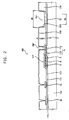
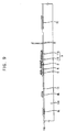
- FIG. 1 is a plan view illustrating a display substrate 100 according to a first embodiment of the present invention.
- FIG. 2 is a cross-sectional view taken along a line I-I' in FIG. 1 .
- the display substrate 100 includes a thin-film transistor (TFT) layer 110, a passivation layer 120, a color filter layer 130, and a pixel electrode 140.
- TFT thin-film transistor
- the TFT layer 110 is formed on a transparent insulation substrate 150.
- the transparent insulation substrate 150 may include glass or plastic.
- the TFT layer 110 includes gate lines GL, data lines DL, a TFT, and storage electrodes SE.
- the data lines DL extend in a direction different from the direction in which the gate lines GL extend.
- a gate insulating layer 111 insulates the data lines DL from the gate lines GL.
- a TFT is electrically connected to each of the gate lines GL and each of the data lines DL.
- the storage electrodes SE are formed from the same layer as the gate lines GL in a pixel region.
- the gate lines GL are formed on the insulation substrate 150.
- the gate lines GL may extend in a first direction and define an upper boundary and a lower boundary for each pixel.
- the gate insulating layer 111 is formed on the insulation substrate 150 having the gate lines GL formed thereon.
- the gate insulation layer 111 protects the gate lines GL and the storage electrodes SE, and electrically insulates the gate lines GL and the storage electrodes SE.
- Examples of insulating materials that can be used for the gate insulating layer 111 include silicon nitride (SiNx), silicon oxide (SiOx), etc. These can be used alone or in combination.
- the data lines DL are formed on the gate insulating layer 111.
- the data lines DL are insulated from the gate lines GL by the gate insulating layer 111.
- the data lines DL may extend in a second direction substantially perpendicular to the first direction, and define a right boundary and a left boundary of each pixel.
- the TFT is electrically connected to the gate lines GL and the data lines DL. At least one TFT is formed in each pixel.
- the TFT receives a data voltage from the data lines DL and applies the data voltage to a pixel electrode 140 in response to a gate voltage applied from the gate lines GL.
- the TFT may include a gate electrode G, an active pattern A, a source electrode S, and a drain electrode D.
- the gate electrode G which is a gate terminal of the TFT, is electrically connected to the gate lines GL,
- the active pattern A is formed on the gate insulating layer 111 corresponding to a position above where the gate electrode G is formed.
- the active pattern A may include a semiconductor layer 112 and an ohmic contact layer 113.
- the semiconductor layer 112 may be formed using amorphous silicon (a-Si)
- the ohmic contact layer 113 may be formed using n+ amorphous silicon that is formed by implanting n-type impurities at a high concentration (n+ a-Si).
- the source electrode S is formed on the active pattern A.
- the source electrode S which is a source terminal of the TFT, is electrically connected to the data lines DL,
- the drain electrode D is formed on the active pattern A and spaced apart from the source electrode S.
- the drain electrode D is a drain terminal of the TFT.
- the drain electrode D is electrically connected to the pixel electrode 140 through a contact hole CNT passing through the passivation layer 120 and the color filter layer 130,
- the data lines DL, the source electrode S, the drain electrode D, and the active pattern A are etched by using the same etching mask.
- the outline of the active pattern A matches an outline of the data lines DL, the source electrode S and the drain electrode D in plan view.
- the storage electrode SE is formed from the same layer as the gate lines GL.
- the storage electrode SE is formed using the same material as the gate lines GL.
- the storage electrode SE is formed between two gate lines GL and extends in a direction substantially parallel to the gate lines GL.
- the gate insulating layer 111 and the passivation layer 120 are formed between the storage electrode SE and the pixel electrode 140.
- the storage electrode SE, the gate insulating layer 111, the passivation layer 120, and the pixel electrode 140 form a storage capacitor Cst.
- a common voltage Vcom may be applied to the storage electrode SE, and the storage capacitor Cst may maintain the data voltage applied to the pixel electrode 140 through the TFT during a frame.
- the passivation layer 120 is formed on the TFT layer 110 including the gate lines GL, the data lines DL, the TFT and the storage electrode SE.
- the passivation layer 120 protects the TFT and electrically insulates the TFT.
- Examples of an insulating material that can be used for the passivation layer 120 include silicon nitride (SiNx), silicon oxide (SiOx), etc. These can be used alone or in combination.
- the color filter layer 130 is formed on the passivation layer 120.
- the color filter layer 130 may include a photosensitive organic composition having a pigment for displaying a color image.
- the color filter layer 130 may include a red color filter, a green color filter and a blue color filter.
- the red color filter includes a photosensitive organic composition having a red pigment for displaying red color.
- the green color filter includes a photosensitive organic composition having a green pigment for displaying green color.
- the blue color filter includes a photosensitive organic composition having a blue pigment for displaying blue color.
- the red color filter, the green color filter and the blue color filter are arranged on the passivation layer 120 in a predetermined pattern.
- the red color filter, the green color filter and the blue color filter may be alternately arranged in the first direction or the second direction substantially perpendicular to the first direction so that there are three color filters in each of the pixels.
- the thickness of the color filter layer 130 may be increased to planarize the display substrate 100.
- the color filter layer 130 may have a thickness of about 2.5 ⁇ m to about 3.5 ⁇ m.
- an organic insulating layer which has been formed as part of a conventional display substrate for planarizing the conventional display substrate may be omitted.
- light transmissivity may be enhanced and costs for manufacturing the display substrate may be reduced.
- the color filter layer 130 includes a storage hole SEH which is formed at a position corresponding to the storage electrode SE.
- the storage hole SEH has a horizontal cross-sectional area greater than the top surface area of the storage electrode SE so it reduces the differences between the capacitances of the red color filter, the green color filter and the blue color filter.
- a “horizontal cross-sectional area,” as used herein, refers to the cross-sectional area when the display substrate 100 is sliced in a plane parallel to the insulation substrate 150. In the case of the storage hole SEH, which has a varying cross-sectional area due to the sidewall being inclined, the "horizontal cross-sectional area" refers to the horizontal cross-sectional area of the narrowest portion.
- the red color filter, the green color filter and the blue color filter are generally formed using the same mask or masks having the same design.
- materials of the red, green and blue color filters are different from each other, so that a thickness, a dielectric constant, and an opening width CD of the storage hole SEH, etc., of each of the red, green and blue color filters may be different from each other.
- the maximum difference in the thicknesses of the red, green and blue color filters may be about 2,000 A, and the maximum difference in the opening widths of the storage holes among the red, green and blue color filters may be about 3 ⁇ m.
- a dielectric constant of the red, green and blue color filters varies in a range of about 3.3 to about 3.5.
- the differences in the thickness, the dielectric constant and the opening width of the storage hole among the red, green and blue color filters change the liquid crystal capacitance Clc, the storage capacitance Cst, and the parasitic capacitance Cgs, all of which may affect electrical characteristics of the pixel. Differences between the kickback voltages Vkb for the red, green and blue color filters are increased by the change in the liquid crystal capacitance Clc, the storage capacitance Cst, and the parasitic capacitance Cgs.
- the differences in the kickback voltages Vkb of the red, green and blue color filters change the grayscale voltage.
- the slope of a graph showing the transmissivity as a function of voltage is increased by the differences between the kickback voltages Vkb in a low grayscale region.
- Variation of the kickback voltage Vkb is mostly caused by a deterioration of the storage capacitance Cst.
- the storage capacitance Cst is determined by an overlapping area between the storage electrode SE and the pixel electrode 140 in a region in which the storage hole is formed.
- differences between the storage capacitances among the red, green and blue pixels are increased, as differences between the opening widths CD among the red, green and blue color filters are increased.
- each of the red, green and blue color filters has a horizontal cross-sectional area greater than the horizontal cross-sectional area of the storage electrode SE, so that an overlapping area between the storage electrode SE and the pixel electrode 140 remains constant. As long as the overlapping area remains constant, there will be no changes to the storage capacitance Cst even if the opening width CD of each of the red, green and blue color filters is changed.
- the opening of each color filter has a horizontal cross-sectional area greater than the horizontal cross-sectional area of the storage electrode SE.
- the horizontal cross-sectional area of the storage hole formed in every pixel is greater than the horizontal cross-sectional area of the storage electrode SE, and the overlapping area between the storage electrode SE and the pixel electrode 140 corresponding to each of the red, green and blue color filters is substantially the same.
- the pixel-to-pixel variation of the kickback voltage Vkb may be decreased and the shifting of color coordinates may be prevented in a low grayscale region. Thus, color reproducibility may be improved.
- the pixel electrode 140 is formed on the color filter layer 130 to correspond to each pixel.
- the pixel electrode 140 is formed using a transparent conductive material to transmit light. Examples of the transparent conductive material that can be used for the pixel electrode 140 include indium zinc oxide (IZO), indium tin oxide (ITO), etc.
- the pixel electrode 140 is electrically connected to the drain electrode D through the contact hole CNT extending through the color filter layer 130 and the passivation layer 120.
- the pixel electrode 140 overlaps the storage electrode SE and the passivation layer 120, and the gate insulating layer 111 is interposed between the pixel electrode 140 and the storage electrode SE. Therefore, the storage capacitor Cst is formed by the pixel electrode 140, the storage electrode SE, the passivation layer 120, and the gate insulating layer 111.
- the pixel electrode 140 may have patterned openings that divide each pixel into a plurality of domains in order to enhance the viewing angle of the LCD apparatus.
- the pixel electrode 140 may be divided into a main electrode and a sub-electrode to which different voltages are applied.
- each pixel may have two TFTs respectively connected to the main electrode and the sub-electrode.
- Each pixel electrode 140 is independently formed in each pixel, and thus an opening may be formed between adjacent pixels to partially expose the color filter layer 130. Impurities may enter the liquid crystal layer through the opening that partially exposes the color filter layer 130, contaminating the liquid crystal layer. In order to prevent the impurities from entering the liquid crystal layer, an inorganic insulating layer (not shown) may be formed on the color filter layer.
- the display substrate 100 may further include a light-blocking part that prevents the light from leaking through the portion between the edge of the storage hole SEH and the edge of the storage electrode SE.
- FIG. 3 is a plan view illustrating a display substrate according to a second embodiment of the present invention.
- FIG. 4 is a cross-sectional view taken along a line II-II' in FIG. 3 .
- FIG. 5 is a plan view illustrating a light-blocking film according to an embodiment of the present invention.
- the display substrate 100 may include a light-blocking layer 160 that prevents the light from leaking through the portion between the edge of the storage hole SEH and the edge of the storage electrode SE.
- the light-blocking layer 160 is formed from the same layer as the data lines DL and is disposed in each pixel.
- the light-blocking layer 160 covers the portion between the edge of the storage hole SEH and the edge of the storage electrode SE.
- the light-blocking layer 160 may extend in a direction in which the gate lines GL extend to cover an upper edge and a lower edge of the storage electrode SE.
- the light-blocking layer 160 may enclose the entire edge of the storage electrode SE as shown in FIG. 5 .
- the light-blocking layer 160 is formed between the edge of the storage hole SEH and the storage electrode SE to prevent the light from a backlight from leaking.
- the light-blocking layer 160 is spaced apart from the data lines DL and is electrically insulated from the storage electrode SE by the gate insulating layer 111 to remain floating. Alternatively, the light-blocking layer 160 may be connected to one of the data lines DL that are disposed on either side of the light-blocking layer 160.
- FIG. 6 is a cross-sectional view illustrating a display substrate according to a third embodiment of the present invention.
- the display substrate 100 may further include a column spacer 170 formed on the pixel electrode 140.
- the column spacer 170 maintains a distance between the display substrate 100 and the cover substrate.
- the column spacer 170 is formed in a region having the storage hole SEH formed thereon and has a horizontal cross-sectional area greater than the horizontal cross-sectional area of the storage hole SEH to prevent light from leaking through the portion between the edge of storage hole SEH and the edge of the storage electrode SE.
- the column spacer 170 may be formed using a material that blocks light.
- the column spacer 170 may be formed using an organic black matrix material.
- FIG. 7 is a cross-sectional view illustrating a display substrate according to a fourth embodiment of the present invention.
- the display substrate 100 may include a column spacer 170 and a light-blocking layer 160.
- the column spacer 170 is formed in a storage hole SEH and has a horizontal cross-sectional area greater than the horizontal cross-sectional area of the storage hole SEH to prevent light from leaking.
- the light-blocking layer 160 is formed on an edge of the column spacer 170 through a process for forming the data lines DL to prevent light from leaking.
- FIGS. 8 to 10 are cross-sectional views illustrating a method of manufacturing a display substrate according to an embodiment of the present invention.
- a gate line GL, a gate electrode G electrically connected to the gate line GL and a storage electrode SE disposed between the gate lines GL are formed on a display substrate 150.
- the gate line GL, the gate electrode G and the storage electrode SE are simultaneously formed in one photolithography process using a single mask.
- a gate insulating layer 111 is formed on the display substrate 150 having the gate line GL, the gate electrode G and the storage electrode SE formed thereon.
- an n+ amorphous silicon (n+ a-Si) layer for forming an ohmic contact layer 113 and a metal layer for data lines are sequentially formed on the gate insulating layer 111.
- An active pattern A, a data line DL, a source electrode S electrically connected to the data line DL and a drain electrode D spaced apart from the source electrode S are formed through one photolithography process using a slit mask or a halftone mask,
- the data line DL, the source electrode S, the drain electrode D, and the active pattern A are simultaneously etched through one photolithography process so that the data line DL, the source electrode S and the drain electrode D have substantially the same outline as the active pattern A.
- a TFT layer 110 is completed.
- a light-blocking layer 180 that prevents light from leaking through an edge of the storage electrode SE is formed in the same process that forms the data line DL, the source electrode S and the drain electrode D.
- the light-blocking layer 160 may be formed from substantially the same layer as the data line DL, the source electrode S and the drain electrode D,
- a passivation layer 120 is formed on the insulating substrate 150 to cover the TFT layer 110.
- a color filter layer 130 including a red color filter, a green color filter and a blue color filter is formed on the passivation layer 120.
- a storage hole corresponding to the storage electrode SE is formed through the color filter layer 130 in order to form a storage capacitor Cst.
- a contact hole CNT exposing the drain electrode D is formed through the color filter layer 130.
- the red, green and blue color filters are regularly arranged on the passivation layer 120 to form a uniform pattern.
- the red, green and blue color filters may be alternately arranged along the first direction or the second direction so that the color filters correspond to the pixels, respectively,
- the red, green and blue color filters are respectively formed in separate photolithography processes.
- the photolithography processes for forming the red, green and blue color filters, respectively, are performed using the same mask or masks having the same design to decrease manufacturing costs.
- the red, green and blue color filters include different materials from each other, so that the thickness, the dielectric constant, and the opening area of the storage hole SEH of each of the red, green and blue color filters of the color Filter layer 130 may be different from each other.
- an overlapping area between the storage electrode SE and the pixel electrode 140 remains uniform even if the sizes of the openings that extend through the red, green and blue color filters are different from each other. Accordingly, differences among the storage capacitances Cst according to the red, green and blue color filters may be decreased.
- a contact hole CNT extending to the drain electrode D is formed through the passivation layer 120.
- the contact hole CNT may be formed before the color filter layer 130 is formed.
- a pixel electrode 140 corresponding to each pixel is formed on the color filter layer 130.
- the pixel electrode 140 is electrically connected to the drain electrode D through the contact hole CNT passing through the color filter layer 130 and the passivation layer 120.
- the pixel electrode 140 overlaps the storage electrode SE and the passivation layer 120, and the gate insulating layer 111 are interposed between the pixel electrode 140 and the storage electrode SE to form a storage capacitor Cst.
- a column spacer 170 may be formed on the pixel electrode 140 to prevent light from leaking through the edge of the storage electrode SE.
- the column spacer 170 has a horizontal cross-sectional area greater than that of the storage electrode SE and is formed using an opaque material that blocks light.
- FIG. 11 is a cross-sectional view illustrating a display apparatus according to an embodiment of the present invention.
- a display apparatus 200 includes a display substrate 100, a cover substrate 300 positioned substantially parallel to the display substrate 100, and a liquid crystal layer 400 disposed between the display substrate 100 and the cover substrate 300.
- the display substrate 100 is substantially the same as the display substrate shown in FIGS. 1 to 7 . Thus, any repetitive explanation concerning the display substrate 100 will be omitted.
- the cover substrate 300 is positioned substantially parallel to the display substrate 100, and the liquid crystal layer 400 is interposed between the display substrate 100 and the cover substrate 300.
- the cover substrate 300 includes an insulating substrate 310 and a common electrode 320 formed on an opposing surface of the insulating substrate 310 facing the display substrate 100.
- the common electrode 320 is formed using a transparent conductive material to transmit light. Examples of the transparent conductive material that can be used for the common electrode 320 include indium zinc oxide (IZO), indium tin oxide (ITO), etc.
- the common electrode 320 may include patterned openings to enhance the viewing angle.
- the cover substrate 300 may further include a black matrix 330.
- the black matrix 330 is formed in a region corresponding to the storage hole SEH and has a horizontal cross-sectional area greater than the horizontal cross-sectional area of the storage hole SEH. Accordingly, the black matrix 330 may prevent light from leaking through the portion between an edge of the storage hole SEH and an edge of the storage electrode SE. Alternately, the black matrix may be formed on the sides of the pixels.
- the liquid crystal layer 400 includes liquid crystal molecules arranged in a predetermined pattern.
- the liquid crystal molecules have optical and electrical properties of anisotropic refraction, anisotropic dielectric constant, etc.
- An electrical field between the pixel electrode 140 and the common electrode 320 changes the arrangement of the liquid crystal molecules to control the amount of light passing through the liquid crystal layer 400.
- an opening of a storage hole formed in red, green and blue color filters has a horizontal cross-sectional area greater than the horizontal cross-sectional area of a storage electrode to minimize the difference among storage capacitors formed in different pixels.
- variation in the kickback voltages of the pixels may be decreased and shifting of color coordinates may be prevented in a low grayscale region.
- a light-blocking layer is formed between an edge of the storage hole and an edge of the storage electrode and/or a column spacer that has a horizontal cross-sectional area greater than the storage hole.
- the light-blocking layer is formed using a material that blocks light in the storage hole. Therefore, the light-blocking layer and/or the column spacer may prevent light from leaking.
Landscapes
- Physics & Mathematics (AREA)
- Nonlinear Science (AREA)
- Engineering & Computer Science (AREA)
- Microelectronics & Electronic Packaging (AREA)
- Mathematical Physics (AREA)
- Chemical & Material Sciences (AREA)
- Crystallography & Structural Chemistry (AREA)
- General Physics & Mathematics (AREA)
- Optics & Photonics (AREA)
- Power Engineering (AREA)
- Liquid Crystal (AREA)
Abstract
Description
- The present invention relates to a display apparatus, More particularly, the present invention relates to a display substrate capable of preventing a color coordinate shift to improve color reproducibility, a display apparatus having the display substrate and a method of manufacturing the display substrate.
- A liquid crystal display (LCD) apparatus includes a display substrate, a cover substrate positioned on the display substrate and a liquid crystal layer disposed between the display substrate and the cover substrate.
- Generally, the display substrate includes a plurality of signal lines to independently drive a plurality of pixels, a plurality of thin-film transistors (TFTs) and a plurality of pixel electrodes. The cover substrate includes a color filter layer having a red color filter, a green color filter and a blue color filter, and a common electrode on the pixel electrode.
- An LCD apparatus that has a color filter on array (COA) structure has been developed. In the LCD apparatus having the COA structure, the color filter layer is formed on the display substrate in order to prevent misalignment between the display substrate and the cover substrate.
- However, in the LCD apparatus having the COA structure, color coordinates become lower in a low grayscale region and then rapidly increase in a specific region. Therefore, colors are shifted in the low grayscale region, making it difficult to display a smooth image.
- The present invention provides a display substrate capable of preventing a color coordinate shift to improve color reproducibility. The present invention further provides a display apparatus having the display substrate. The present invention still further provides a method of manufacturing the display substrate.
- In one aspect, the invention is a display substrate that includes a substrate, a thin-film transistor (TFT) layer formed on the substrate, a color filter layer and a pixel electrode. The TFT layer includes a gate line, a data line electrically insulated from the gate line by a gate insulating layer, a TFT electrically connected to the gate line and the data line, and a storage electrode formed in each pixel that is defined by the gate line and the data line that extends in a direction different from the gate line. The storage electrode is formed from the same layer as the gate line. The color filter layer includes a storage hole extending to a portion of the TFT layer corresponding to the storage electrode. The storage hole has a horizontal cross-sectional area greater than the storage electrode. The pixel electrode is formed on the color filter layer and in the storage hole over the storage electrode to form a storage capacitor. The gate insulating layer is interposed between the pixel electrode and the storage electrode.
- The color filter layer may include a red color filter, a green color filter and a blue color filter formed in each pixel.
- The display substrate may further include a light-blocking layer covering an area between an edge portion of the storage hole and an edge portion of the storage electrode.
- The display substrate may further include a column spacer formed on the pixel electrode. The column spacer may have a horizontal cross-sectional area greater than the storage hole, and may be formed using a material that blocks light.
- In another aspect, the invention is a display apparatus that includes the above-described display substrate, a cover substrate and a liquid crystal layer. The cover substrate is positioned substantially parallel to the display substrate and includes a common electrode formed on a surface of the cover substrate that faces the display substrate. The liquid crystal layer is disposed between the display substrate and the cover substrate,
- In yet another aspect, the invention is a method of manufacturing a display substrate by providing a substrate and forming a TFT layer thereon, The TFT layer includes a gate line, a data line, a TFT, and a storage electrode. The data line is insulated from the gate line by a gate insulating layer and crosses the gate line. The TFT is connected to the gate line and the data line. The storage electrode is formed through a process for forming the gate lines in each pixel. A color filter layer is formed. The color filter layer includes a storage hole extending to a portion of the TFT layer corresponding to the storage electrode and having a horizontal cross-sectional area greater than the storage electrode, wherein the horizontal cross-sectional area is measured in a plane parallel to the substrate. The method further entails forming a pixel electrode. The pixel electrode is formed on the color filter layer and in the storage hole, and overlaps the storage electrode. The gate insulating layer is interposed between the pixel electrode and the storage electrode. Therefore, a storage capacitor is formed by the pixel electrode, the storage electrode and the gate insulating layer.
- The color filter layer may be formed by forming a red color filter, a green color filter and a blue color filter. The red color filter, the green color filter and the blue color filter are formed using masks having substantially the same design.
- According to the display substrate, the display apparatus and the method of the present invention, color coordinates may not be shifted in a low grayscale. Thus, colors may not be changed in the low grayscale.
- The above and other features and advantages of the present invention will become more apparent by describing in detailed embodiments thereof with reference to the accompanying drawings, in which:
-
FIG. 1 is a plan view illustrating a display substrate according to a first embodiment of the present invention; -
FIG, 2 is a cross-sectional view taken along a line I-I' inFIG, 1 ; -
FIG. 3 is a plan view illustrating a display substrate according to a second embodiment of the present invention; -
FIG. 4 is a cross-sectional view taken along a line II-II' inFIG. 3 ; -
FIG. 5 is a plan view illustrating a light-blocking film according to an embodiment of the present invention; -
FIG. 6 is a cross-sectional view illustrating a display substrate according to a third embodiment of the present invention; -
FIG. 7 is a cross-sectional view illustrating a display substrate according to a fourth embodiment of the present invention; -
FIGS, 8 to 10 are cross-sectional views illustrating a method of manufacturing a display substrate according to an embodiment of the present invention; and -
FIG. 11 is a cross-sectional view illustrating a display apparatus according to an embodiment of the present invention. - The invention is described more fully hereinafter with reference to the accompanying drawings, in which embodiments of the invention are shown. This invention may, however, be embodied in many different forms and should not be construed as limited to the embodiments set forth herein, Rather, these embodiments are provided so that this disclosure will be thorough and complete, and will fully convey the scope of the invention to those skilled in the art. In the drawings, the size and relative sizes of layers and regions may be exaggerated for clarity.
- It will be understood that when an element or layer is referred to as being "on," "connected to" or "coupled to" another element or layer, it can be directly on, connected or coupled to the other element or layer or intervening elements or layers may be present. In contrast, when an element is referred to as being "directly on," "directly connected to" or "directly coupled to" another element or layer, there are no intervening elements or layers present. Like numbers refer to like elements throughout, As used herein, the term "and/or" includes any and all combinations of one or more of the associated listed items.
- It will be understood that, although the terms first, second, third etc. may be used herein to describe various elements, components, regions, layers and/or sections, these elements, components, regions, layers and/or sections should not be limited by these terms. These terms are only used to distinguish one element, component, region, layer or section from another region, layer or section. Thus, a first element, component, region, layer or section discussed below could be termed a second element, component, region, layer or section without departing from the teachings of the present invention.
- Spatially relative terms, such as "beneath," "below," "lower," "above," "upper" and the like, may be used herein for ease of description to describe one element or feature's relationship to another element(s) or feature(s) as illustrated in the figures. It will be understood that the spatially relative terms are intended to encompass different orientations of the device in use or operation in addition to the orientation depicted in the figures, For example, if the device in the figures is turned over, elements described as "below" or "beneath" other elements or features would then be oriented "above" the other elements or features. Thus, the term "below" can encompass both an orientation of above and below. The device may be otherwise oriented (rotated 90 degrees or at other orientations) and the spatially relative descriptors used herein interpreted accordingly.
- The terminology used herein is for the purpose of describing particular embodiments only and is not intended to be limiting of the invention. As used herein, the singular forms "a," "an" and "the" are intended to include the plural forms as well, unless the context clearly indicates otherwise. It will be further understood that the terms "comprises" and/or "comprising," when used in this specification. specify the presence of stated features, integers, steps, operations, elements, and/or components, but do not preclude the presence or addition of one or more other features, integers, steps, operations, elements, components, and/or groups thereof.
- Embodiments of the invention are described herein with reference to cross-sectional illustrations that are schematic illustrations of idealized embodiments (and intermediate structures) of the invention. As such, variations from the shapes of the illustrations as a result, for example, of manufacturing techniques and/or tolerances, are to be expected. Thus, embodiments of the invention should not be construed as limited to the particular shapes of regions illustrated herein but are to include deviations in shapes that result, for example, from manufacturing. For example, an implanted region illustrated as a rectangle will, typically, have rounded or curved features and/or a gradient of implant concentration at its edges rather than a binary change from implanted to non-implanted region. Likewise, a buried region formed by implantation may result in some implantation in the region between the buried region and the surface through which the implantation takes place. Thus, the regions illustrated in the figures are schematic in nature and their shapes are not intended to illustrate the actual shape of a region of a device and are not intended to limit the scope of the invention.
- Unless otherwise defined, all terms (including technical and scientific terms) used herein have the same meaning as commonly understood by one of ordinary skill in the art to which this invention belongs, It will be further understood that terms, such as those defined in commonly used dictionaries, should be interpreted as having a meaning that is consistent with their meaning in the context of the relevant art and will not be interpreted in an idealized or overly formal sense unless expressly so defined herein.
- Hereinafter, the present invention will be explained in detail with reference to the accompanying drawings.
-
FIG. 1 is a plan view illustrating adisplay substrate 100 according to a first embodiment of the present invention.FIG. 2 is a cross-sectional view taken along a line I-I' inFIG. 1 . - Referring to
FIGS. 1 and2 , thedisplay substrate 100 includes a thin-film transistor (TFT)layer 110, apassivation layer 120, acolor filter layer 130, and apixel electrode 140. - The
TFT layer 110 is formed on atransparent insulation substrate 150. Thetransparent insulation substrate 150 may include glass or plastic. - The
TFT layer 110 includes gate lines GL, data lines DL, a TFT, and storage electrodes SE. The data lines DL extend in a direction different from the direction in which the gate lines GL extend. Agate insulating layer 111 insulates the data lines DL from the gate lines GL. A TFT is electrically connected to each of the gate lines GL and each of the data lines DL. The storage electrodes SE are formed from the same layer as the gate lines GL in a pixel region. - The gate lines GL are formed on the
insulation substrate 150. For example, the gate lines GL may extend in a first direction and define an upper boundary and a lower boundary for each pixel. - The
gate insulating layer 111 is formed on theinsulation substrate 150 having the gate lines GL formed thereon. Thegate insulation layer 111 protects the gate lines GL and the storage electrodes SE, and electrically insulates the gate lines GL and the storage electrodes SE. Examples of insulating materials that can be used for thegate insulating layer 111 include silicon nitride (SiNx), silicon oxide (SiOx), etc. These can be used alone or in combination. - The data lines DL are formed on the
gate insulating layer 111. The data lines DL are insulated from the gate lines GL by thegate insulating layer 111. For example, the data lines DL may extend in a second direction substantially perpendicular to the first direction, and define a right boundary and a left boundary of each pixel. - The TFT is electrically connected to the gate lines GL and the data lines DL. At least one TFT is formed in each pixel. The TFT receives a data voltage from the data lines DL and applies the data voltage to a
pixel electrode 140 in response to a gate voltage applied from the gate lines GL. - The TFT may include a gate electrode G, an active pattern A, a source electrode S, and a drain electrode D.
- The gate electrode G, which is a gate terminal of the TFT, is electrically connected to the gate lines GL,
- The active pattern A is formed on the
gate insulating layer 111 corresponding to a position above where the gate electrode G is formed. The active pattern A may include asemiconductor layer 112 and anohmic contact layer 113. For example, thesemiconductor layer 112 may be formed using amorphous silicon (a-Si), and theohmic contact layer 113 may be formed using n+ amorphous silicon that is formed by implanting n-type impurities at a high concentration (n+ a-Si). - The source electrode S is formed on the active pattern A. The source electrode S, which is a source terminal of the TFT, is electrically connected to the data lines DL,
- The drain electrode D is formed on the active pattern A and spaced apart from the source electrode S. The drain electrode D is a drain terminal of the TFT. The drain electrode D is electrically connected to the
pixel electrode 140 through a contact hole CNT passing through thepassivation layer 120 and thecolor filter layer 130, - The data lines DL, the source electrode S, the drain electrode D, and the active pattern A are etched by using the same etching mask. Thus, the outline of the active pattern A matches an outline of the data lines DL, the source electrode S and the drain electrode D in plan view.
- The storage electrode SE is formed from the same layer as the gate lines GL. Thus, the storage electrode SE is formed using the same material as the gate lines GL. In one embodiment, the storage electrode SE is formed between two gate lines GL and extends in a direction substantially parallel to the gate lines GL.
- The
gate insulating layer 111 and thepassivation layer 120 are formed between the storage electrode SE and thepixel electrode 140. Thus, the storage electrode SE, thegate insulating layer 111, thepassivation layer 120, and thepixel electrode 140 form a storage capacitor Cst. A common voltage Vcom may be applied to the storage electrode SE, and the storage capacitor Cst may maintain the data voltage applied to thepixel electrode 140 through the TFT during a frame. - The
passivation layer 120 is formed on theTFT layer 110 including the gate lines GL, the data lines DL, the TFT and the storage electrode SE. Thepassivation layer 120 protects the TFT and electrically insulates the TFT. Examples of an insulating material that can be used for thepassivation layer 120 include silicon nitride (SiNx), silicon oxide (SiOx), etc. These can be used alone or in combination. - The
color filter layer 130 is formed on thepassivation layer 120. Thecolor filter layer 130 may include a photosensitive organic composition having a pigment for displaying a color image. For example, thecolor filter layer 130 may include a red color filter, a green color filter and a blue color filter. The red color filter includes a photosensitive organic composition having a red pigment for displaying red color. The green color filter includes a photosensitive organic composition having a green pigment for displaying green color. The blue color filter includes a photosensitive organic composition having a blue pigment for displaying blue color. The red color filter, the green color filter and the blue color filter are arranged on thepassivation layer 120 in a predetermined pattern. For example, the red color filter, the green color filter and the blue color filter may be alternately arranged in the first direction or the second direction substantially perpendicular to the first direction so that there are three color filters in each of the pixels. - The thickness of the
color filter layer 130 may be increased to planarize thedisplay substrate 100. For example, thecolor filter layer 130 may have a thickness of about 2.5 µm to about 3.5 µm. When thecolor filter layer 130 is formed not as part of a cover substrate but as part of a display substrate, an organic insulating layer which has been formed as part of a conventional display substrate for planarizing the conventional display substrate may be omitted. Thus, light transmissivity may be enhanced and costs for manufacturing the display substrate may be reduced. - In order to increase the electrostatic capacity of the storage capacitor Cst, the
color filter layer 130 includes a storage hole SEH which is formed at a position corresponding to the storage electrode SE. The storage hole SEH has a horizontal cross-sectional area greater than the top surface area of the storage electrode SE so it reduces the differences between the capacitances of the red color filter, the green color filter and the blue color filter. A "horizontal cross-sectional area," as used herein, refers to the cross-sectional area when thedisplay substrate 100 is sliced in a plane parallel to theinsulation substrate 150. In the case of the storage hole SEH, which has a varying cross-sectional area due to the sidewall being inclined, the "horizontal cross-sectional area" refers to the horizontal cross-sectional area of the narrowest portion. - When the
color filter layer 130 is formed, the red color filter, the green color filter and the blue color filter are generally formed using the same mask or masks having the same design. In case ofFIGS. 1 and2 , materials of the red, green and blue color filters are different from each other, so that a thickness, a dielectric constant, and an opening width CD of the storage hole SEH, etc., of each of the red, green and blue color filters may be different from each other. For example, when a panel size of a liquid crystal display (LCD) apparatus having thedisplay substrate 100 is about 40 inches, the maximum difference in the thicknesses of the red, green and blue color filters may be about 2,000 A, and the maximum difference in the opening widths of the storage holes among the red, green and blue color filters may be about 3 µm. Also, a dielectric constant of the red, green and blue color filters varies in a range of about 3.3 to about 3.5. - The differences in the thickness, the dielectric constant and the opening width of the storage hole among the red, green and blue color filters change the liquid crystal capacitance Clc, the storage capacitance Cst, and the parasitic capacitance Cgs, all of which may affect electrical characteristics of the pixel. Differences between the kickback voltages Vkb for the red, green and blue color filters are increased by the change in the liquid crystal capacitance Clc, the storage capacitance Cst, and the parasitic capacitance Cgs.
- When the LCD apparatus is alternately driven by a signal having a negative polarity and a signal having a positive polarity with reference to the common voltage Vcom, the differences in the kickback voltages Vkb of the red, green and blue color filters change the grayscale voltage. When the differences between the kickback voltages Vkb are increased, the slope of a graph showing the transmissivity as a function of voltage is increased by the differences between the kickback voltages Vkb in a low grayscale region. Thus, even though the same pixel voltage is applied to the red, green and blue color filters, differences between the gamma voltages of a red pixel, a green pixel and a blue pixel remarkably change color coordinates in the low grayscale region.
- Variation of the kickback voltage Vkb is mostly caused by a deterioration of the storage capacitance Cst. The storage capacitance Cst is determined by an overlapping area between the storage electrode SE and the
pixel electrode 140 in a region in which the storage hole is formed. Thus, differences between the storage capacitances among the red, green and blue pixels are increased, as differences between the opening widths CD among the red, green and blue color filters are increased. - The opening of each of the red, green and blue color filters has a horizontal cross-sectional area greater than the horizontal cross-sectional area of the storage electrode SE, so that an overlapping area between the storage electrode SE and the
pixel electrode 140 remains constant. As long as the overlapping area remains constant, there will be no changes to the storage capacitance Cst even if the opening width CD of each of the red, green and blue color filters is changed. When the smallest opening in the red, green and blue color filters has a horizontal cross-sectional area greater than the horizontal cross-sectional area of the storage electrode SE, the opening of each color filter has a horizontal cross-sectional area greater than the horizontal cross-sectional area of the storage electrode SE. - When the opening width CD of each of the red, green and blue color filters is greater than the width SD of storage electrode SE, the horizontal cross-sectional area of the storage hole formed in every pixel is greater than the horizontal cross-sectional area of the storage electrode SE, and the overlapping area between the storage electrode SE and the
pixel electrode 140 corresponding to each of the red, green and blue color filters is substantially the same. - When the differences in the storage capacitances Cst of the red, green and blue pixels are decreased, the pixel-to-pixel variation of the kickback voltage Vkb may be decreased and the shifting of color coordinates may be prevented in a low grayscale region. Thus, color reproducibility may be improved.
- The
pixel electrode 140 is formed on thecolor filter layer 130 to correspond to each pixel. Thepixel electrode 140 is formed using a transparent conductive material to transmit light. Examples of the transparent conductive material that can be used for thepixel electrode 140 include indium zinc oxide (IZO), indium tin oxide (ITO), etc. - The
pixel electrode 140 is electrically connected to the drain electrode D through the contact hole CNT extending through thecolor filter layer 130 and thepassivation layer 120. Thepixel electrode 140 overlaps the storage electrode SE and thepassivation layer 120, and thegate insulating layer 111 is interposed between thepixel electrode 140 and the storage electrode SE. Therefore, the storage capacitor Cst is formed by thepixel electrode 140, the storage electrode SE, thepassivation layer 120, and thegate insulating layer 111. - The
pixel electrode 140 may have patterned openings that divide each pixel into a plurality of domains in order to enhance the viewing angle of the LCD apparatus. Alternatively, thepixel electrode 140 may be divided into a main electrode and a sub-electrode to which different voltages are applied. When thepixel electrode 140 is divided into the main electrode and the sub-electrode, each pixel may have two TFTs respectively connected to the main electrode and the sub-electrode. - Each
pixel electrode 140 is independently formed in each pixel, and thus an opening may be formed between adjacent pixels to partially expose thecolor filter layer 130. Impurities may enter the liquid crystal layer through the opening that partially exposes thecolor filter layer 130, contaminating the liquid crystal layer. In order to prevent the impurities from entering the liquid crystal layer, an inorganic insulating layer (not shown) may be formed on the color filter layer. - When the opening of the storage hole SEH has a horizontal cross-sectional area greater than the horizontal cross-sectional area of the storage electrode SE, light may leak through a portion between an edge of the storage hole SEH and an edge of the storage electrode SE. Therefore, the
display substrate 100 may further include a light-blocking part that prevents the light from leaking through the portion between the edge of the storage hole SEH and the edge of the storage electrode SE. -
FIG. 3 is a plan view illustrating a display substrate according to a second embodiment of the present invention.FIG. 4 is a cross-sectional view taken along a line II-II' inFIG. 3 .FIG. 5 is a plan view illustrating a light-blocking film according to an embodiment of the present invention. - Referring to
FIGS. 3, 4 and5 , thedisplay substrate 100 may include a light-blocking layer 160 that prevents the light from leaking through the portion between the edge of the storage hole SEH and the edge of the storage electrode SE. - The light-
blocking layer 160 is formed from the same layer as the data lines DL and is disposed in each pixel. The light-blocking layer 160 covers the portion between the edge of the storage hole SEH and the edge of the storage electrode SE. For example, the light-blocking layer 160 may extend in a direction in which the gate lines GL extend to cover an upper edge and a lower edge of the storage electrode SE. The light-blocking layer 160 may enclose the entire edge of the storage electrode SE as shown inFIG. 5 . The light-blocking layer 160 is formed between the edge of the storage hole SEH and the storage electrode SE to prevent the light from a backlight from leaking. - The light-
blocking layer 160 is spaced apart from the data lines DL and is electrically insulated from the storage electrode SE by thegate insulating layer 111 to remain floating. Alternatively, the light-blocking layer 160 may be connected to one of the data lines DL that are disposed on either side of the light-blocking layer 160. -
FIG. 6 is a cross-sectional view illustrating a display substrate according to a third embodiment of the present invention. - Referring to
FIG. 6 , thedisplay substrate 100 may further include acolumn spacer 170 formed on thepixel electrode 140. Thecolumn spacer 170 maintains a distance between thedisplay substrate 100 and the cover substrate. - The
column spacer 170 is formed in a region having the storage hole SEH formed thereon and has a horizontal cross-sectional area greater than the horizontal cross-sectional area of the storage hole SEH to prevent light from leaking through the portion between the edge of storage hole SEH and the edge of the storage electrode SE. Thecolumn spacer 170 may be formed using a material that blocks light. For example, thecolumn spacer 170 may be formed using an organic black matrix material. -
FIG. 7 is a cross-sectional view illustrating a display substrate according to a fourth embodiment of the present invention. - Referring to
FIG. 7 , thedisplay substrate 100 may include acolumn spacer 170 and a light-blocking layer 160. - The
column spacer 170 is formed in a storage hole SEH and has a horizontal cross-sectional area greater than the horizontal cross-sectional area of the storage hole SEH to prevent light from leaking. The light-blocking layer 160 is formed on an edge of thecolumn spacer 170 through a process for forming the data lines DL to prevent light from leaking. - Hereinafter, a method of manufacturing the display substrate according to another embodiment of the present invention will be described.
-
FIGS. 8 to 10 are cross-sectional views illustrating a method of manufacturing a display substrate according to an embodiment of the present invention. - Referring to
FIGS. 1 and8 , a gate line GL, a gate electrode G electrically connected to the gate line GL and a storage electrode SE disposed between the gate lines GL are formed on adisplay substrate 150. The gate line GL, the gate electrode G and the storage electrode SE are simultaneously formed in one photolithography process using a single mask. - Referring to
FIGS. 1 and9 , agate insulating layer 111 is formed on thedisplay substrate 150 having the gate line GL, the gate electrode G and the storage electrode SE formed thereon. - An amorphous silicon (a-Si) layer for forming a
semiconductor layer 112, an n+ amorphous silicon (n+ a-Si) layer for forming anohmic contact layer 113 and a metal layer for data lines are sequentially formed on thegate insulating layer 111. An active pattern A, a data line DL, a source electrode S electrically connected to the data line DL and a drain electrode D spaced apart from the source electrode S are formed through one photolithography process using a slit mask or a halftone mask, The data line DL, the source electrode S, the drain electrode D, and the active pattern A are simultaneously etched through one photolithography process so that the data line DL, the source electrode S and the drain electrode D have substantially the same outline as the active pattern A. Thus, aTFT layer 110 is completed. - As shown in
FIGS. 4 and7 , a light-blocking layer 180 that prevents light from leaking through an edge of the storage electrode SE is formed in the same process that forms the data line DL, the source electrode S and the drain electrode D. In some embodiments, the light-blocking layer 160 may be formed from substantially the same layer as the data line DL, the source electrode S and the drain electrode D, - Referring to
FIGS. 1 and10 , apassivation layer 120 is formed on the insulatingsubstrate 150 to cover theTFT layer 110. - A
color filter layer 130 including a red color filter, a green color filter and a blue color filter is formed on thepassivation layer 120. A storage hole corresponding to the storage electrode SE is formed through thecolor filter layer 130 in order to form a storage capacitor Cst. Also, a contact hole CNT exposing the drain electrode D is formed through thecolor filter layer 130. - The red, green and blue color filters are regularly arranged on the
passivation layer 120 to form a uniform pattern. For example, the red, green and blue color filters may be alternately arranged along the first direction or the second direction so that the color filters correspond to the pixels, respectively, - The red, green and blue color filters are respectively formed in separate photolithography processes. The photolithography processes for forming the red, green and blue color filters, respectively, are performed using the same mask or masks having the same design to decrease manufacturing costs. The red, green and blue color filters include different materials from each other, so that the thickness, the dielectric constant, and the opening area of the storage hole SEH of each of the red, green and blue color filters of the
color Filter layer 130 may be different from each other. - When an opening that extends through each of the red, green and blue color filters has a horizontal cross-sectional area greater than that of the storage electrode SE, an overlapping area between the storage electrode SE and the
pixel electrode 140 remains uniform even if the sizes of the openings that extend through the red, green and blue color filters are different from each other. Accordingly, differences among the storage capacitances Cst according to the red, green and blue color filters may be decreased. - A contact hole CNT extending to the drain electrode D is formed through the
passivation layer 120. The contact hole CNT may be formed before thecolor filter layer 130 is formed. - Referring to
FIG. 2 , apixel electrode 140 corresponding to each pixel is formed on thecolor filter layer 130. Thepixel electrode 140 is electrically connected to the drain electrode D through the contact hole CNT passing through thecolor filter layer 130 and thepassivation layer 120. In addition, thepixel electrode 140 overlaps the storage electrode SE and thepassivation layer 120, and thegate insulating layer 111 are interposed between thepixel electrode 140 and the storage electrode SE to form a storage capacitor Cst. - As shown in
FIGS. 6 and7 , acolumn spacer 170 may be formed on thepixel electrode 140 to prevent light from leaking through the edge of the storage electrode SE. Thecolumn spacer 170 has a horizontal cross-sectional area greater than that of the storage electrode SE and is formed using an opaque material that blocks light. -
FIG. 11 is a cross-sectional view illustrating a display apparatus according to an embodiment of the present invention. - Referring to
FIG. 11 , adisplay apparatus 200 includes adisplay substrate 100, acover substrate 300 positioned substantially parallel to thedisplay substrate 100, and aliquid crystal layer 400 disposed between thedisplay substrate 100 and thecover substrate 300. - The
display substrate 100 is substantially the same as the display substrate shown inFIGS. 1 to 7 . Thus, any repetitive explanation concerning thedisplay substrate 100 will be omitted. - The
cover substrate 300 is positioned substantially parallel to thedisplay substrate 100, and theliquid crystal layer 400 is interposed between thedisplay substrate 100 and thecover substrate 300. Thecover substrate 300 includes an insulatingsubstrate 310 and acommon electrode 320 formed on an opposing surface of the insulatingsubstrate 310 facing thedisplay substrate 100. Thecommon electrode 320 is formed using a transparent conductive material to transmit light. Examples of the transparent conductive material that can be used for thecommon electrode 320 include indium zinc oxide (IZO), indium tin oxide (ITO), etc. Thecommon electrode 320 may include patterned openings to enhance the viewing angle. - The
cover substrate 300 may further include ablack matrix 330. Theblack matrix 330 is formed in a region corresponding to the storage hole SEH and has a horizontal cross-sectional area greater than the horizontal cross-sectional area of the storage hole SEH. Accordingly, theblack matrix 330 may prevent light from leaking through the portion between an edge of the storage hole SEH and an edge of the storage electrode SE. Alternately, the black matrix may be formed on the sides of the pixels. - The
liquid crystal layer 400 includes liquid crystal molecules arranged in a predetermined pattern. The liquid crystal molecules have optical and electrical properties of anisotropic refraction, anisotropic dielectric constant, etc. An electrical field between thepixel electrode 140 and thecommon electrode 320 changes the arrangement of the liquid crystal molecules to control the amount of light passing through theliquid crystal layer 400. - According to the display substrate, the display apparatus having the display substrate, and the method of manufacturing the display substrate described above, an opening of a storage hole formed in red, green and blue color filters has a horizontal cross-sectional area greater than the horizontal cross-sectional area of a storage electrode to minimize the difference among storage capacitors formed in different pixels. As a result, variation in the kickback voltages of the pixels may be decreased and shifting of color coordinates may be prevented in a low grayscale region.
- A light-blocking layer is formed between an edge of the storage hole and an edge of the storage electrode and/or a column spacer that has a horizontal cross-sectional area greater than the storage hole. The light-blocking layer is formed using a material that blocks light in the storage hole. Therefore, the light-blocking layer and/or the column spacer may prevent light from leaking.
- Having described the exemplary embodiments of the present invention and its advantage, it is noted that various changes, substitutions and alterations can be made herein without departing from the spirit and scope of the invention as defined by appended claims.
Claims (27)
- A display substrate comprising:a substrate;a thin-film transistor (TFT) layer formed on the substrate, the TFT layer including a gate line, a data line electrically insulated from the gate line by a gate insulating layer and extended in a direction different from the gate line, a TFT electrically connected to the gate line and the data line, and a storage electrode formed in each pixel, wherein the storage electrode is formed from a same layer as the gate line;a color filter layer including a storage hole extending to a portion of the TFT layer corresponding to the storage electrode, the storage hole having a horizontal cross-sectional area greater than the storage electrode, wherein the horizontal cross-sectional area is measured in a plane parallel to the substrate; anda pixel electrode formed on the color filter layer and in the storage hole over the storage electrode to form a storage capacitor, the gate insulating layer being interposed between the pixel electrode and the storage electrode.
- The display substrate of claim 1, wherein the color filter layer comprises a red color filter, a green color filter and a blue color filter formed in each pixel.
- The display substrate of claim 2, wherein the color filter layer has a thickness of about 2.5 µm to about 3.5 µm and a maximum difference in thicknesses of the red, green and blue color filters is about 2,000 A.
- The display substrate of claim 2, the maximum difference in the opening widths of the storage holes among the red, green and blue color filters is about 3 µm, and a dielectric constant of each of the red, green and blue color filters is in a range of about 3.3 to about 3.5.
- The display substrate of claim 1, further comprising a light-blocking layer covering an area between an edge portion of the storage hole and an edge portion of the storage electrode.
- The display substrate of claim 5, wherein the light-blocking layer is formed from a same layer as the data line.
- The display substrate of claim 6, wherein the light-blocking layer is in a floating state.
- The display substrate of claim 1, further comprising a column spacer formed on the pixel electrode, the column spacer having a horizontal cross-sectional area greater than the storage hole.
- The display substrate of claim 8, wherein the column spacer is formed using a material that blocks light,
- The display substrate of claim 9, further comprising a light-blocking layer formed from a same layer as the data line and disposed at an edge portion of the column spacer.
- A display apparatus comprising:a display substrate including:a substrate;a TFT layer formed on the substrate, the TFT layer including a gate line, a data line electrically insulated from the gate line by a gate insulating layer and extended in a direction different from the gate line, a TFT electrically connected to the gate line and the data line, and a storage electrode formed in each pixel, wherein the storage electrode is formed from a same layer as the gate line;a color filter layer including a storage hole extending to a portion of the TFT layer corresponding to the storage electrode, the storage hole having a horizontal cross-sectional area greater than the storage electrode, wherein the cross-sectional area is measured in a plane parallel to the substrate; anda pixel electrode formed on the color filter layer and in the storage hole to overlap the storage electrode and form a storage capacitor, the gate insulating layer being interposed between the pixel electrode and the storage electrode;a cover substrate positioned substantially parallel to the display substrate, the cover substrate including a common electrode formed on a surface of the cover substrate that faces the display substrate; anda liquid crystal layer disposed between the display substrate and the cover substrate.
- The display apparatus of claim 11, wherein the display substrate further comprises a light-blocking layer that is formed from a same layer as the data line and covers a portion between an edge of the storage hole and an edge of the storage electrode.
- The display apparatus of claim 11, wherein the display substrate further comprises a column spacer that is formed on the pixel electrode corresponding to the storage hole and has a horizontal cross-sectional area greater than the storage hole.
- The display apparatus of claim 13, wherein the column spacer is formed using a material that blocks light.
- The display apparatus of claim 13, wherein the display substrate further comprises a light-blocking layer which is formed from a same layer as the data line and is disposed at an edge of the column spacer.
- The display apparatus of claim 11, wherein the cover substrate further comprises a black matrix that corresponds to the storage hole and has a horizontal crass-sectional area greater than the storage hole.
- The display apparatus of claim 16, wherein the display substrate further comprises a light-blocking layer that is formed from a same layer as the data line and corresponds to an edge portion of the black matrix.
- The display apparatus of claim 16, wherein the display substrate further comprises a column spacer that is formed on the pixel electrode corresponding to the storage hole and has a horizontal cross-sectional area greater than the storage hole.
- The display apparatus of claim 14, wherein the column spacer is formed using a material that blocks light.
- The display apparatus of claim 14, wherein the display substrate further comprises a light-blocking layer which is formed from a same layer as the data line and is disposed at an edge portion of the column spacer,
- A method of manufacturing a display substrate, comprising:providing a substrate;forming a TFT layer on the substrate, the TFT layer including a gate line, a data line electrically insulated from the gate line by a gate insulating layer, a TFT electrically connected to the gate line and the data line, and a storage electrode formed from a same layer as the gate lines in each pixel, the data line extending in a direction different from the gate line;forming a color filter layer including a storage hole extending to a portion of the TFT layer corresponding to the storage electrode, the storage hole having a horizontal cross-sectional area greater than the storage electrode, wherein the horizontal cross-sectional area is measured in a plane parallel to the substrate; andforming a pixel electrode on the color filter layer and in the storage hole, the pixel electrode overlapping the storage electrode to form a storage capacitor, the gate insulating layer being interposed between the pixel electrode and the storage electrode.
- The method of claim 21, wherein forming the color filter layer comprises:forming a red color filter;forming a green color filter; andforming a blue color filter.
- The method of claim 22, wherein the red color filter, the green color filter and the blue color filter are formed using masks having a same design.
- The method of claim 21, wherein the TFT layer further comprises a light-blocking layer which is formed from a same layer as the data line and covers a portion between an edge of the storage hole and an edge of the storage electrode.
- The method of claim 21, further comprising forming a column spacer which is formed on the pixel electrode corresponding to the storage hole and has a horizontal cross-sectional area greater than the storage hole.
- The method of claim 25, wherein forming the column spacer comprises using a material that blocks light.
- The method of claim 26, further comprising forming a light-blocking layer from a same layer as the data line, the light-blocking layer being disposed at an end portion of the column spacer.
Applications Claiming Priority (1)
| Application Number | Priority Date | Filing Date | Title |
|---|---|---|---|
| KR1020070012501A KR101377456B1 (en) | 2007-02-07 | 2007-02-07 | Display substrate, method of manufacturing thereof and display apparatus having the same |
Publications (2)
| Publication Number | Publication Date |
|---|---|
| EP1956426A1 true EP1956426A1 (en) | 2008-08-13 |
| EP1956426B1 EP1956426B1 (en) | 2016-01-06 |
Family
ID=39363788
Family Applications (1)
| Application Number | Title | Priority Date | Filing Date |
|---|---|---|---|
| EP08002089.4A Not-in-force EP1956426B1 (en) | 2007-02-07 | 2008-02-05 | Display substrate including a colour filter and storage capacitors and method of manufacturing it |
Country Status (4)
| Country | Link |
|---|---|
| US (1) | US7915614B2 (en) |
| EP (1) | EP1956426B1 (en) |
| KR (1) | KR101377456B1 (en) |
| CN (1) | CN101304034B (en) |
Cited By (1)
| Publication number | Priority date | Publication date | Assignee | Title |
|---|---|---|---|---|
| EP2354839A1 (en) * | 2009-12-17 | 2011-08-10 | AU Optronics Corporation | Liquid crystal display |
Families Citing this family (15)
| Publication number | Priority date | Publication date | Assignee | Title |
|---|---|---|---|---|
| JP5154261B2 (en) | 2008-02-26 | 2013-02-27 | 株式会社ジャパンディスプレイイースト | Liquid crystal display |
| JP5464638B2 (en) * | 2008-08-05 | 2014-04-09 | 株式会社ジャパンディスプレイ | Display element |
| KR102113024B1 (en) * | 2008-09-19 | 2020-06-02 | 가부시키가이샤 한도오따이 에네루기 켄큐쇼 | Display device |
| US20100224880A1 (en) * | 2009-03-05 | 2010-09-09 | Semiconductor Energy Laboratory Co., Ltd. | Semiconductor device |
| KR101610846B1 (en) * | 2009-09-08 | 2016-04-11 | 삼성디스플레이 주식회사 | Display device and manufacturing method thereof |
| KR101607636B1 (en) | 2009-11-23 | 2016-04-12 | 삼성디스플레이 주식회사 | Liquid crystal display |
| CN102402043A (en) * | 2011-11-03 | 2012-04-04 | 深圳市华星光电技术有限公司 | Pixel array and manufacturing method thereof |
| KR102185786B1 (en) * | 2014-02-27 | 2020-12-03 | 삼성디스플레이 주식회사 | Liquid crystal display and method of driving the same |
| CN105044973B (en) * | 2015-08-27 | 2018-07-10 | 深圳市华星光电技术有限公司 | COA type liquid crystal display panels |
| KR102542186B1 (en) * | 2016-04-04 | 2023-06-13 | 삼성디스플레이 주식회사 | Display device |
| KR102816650B1 (en) * | 2016-12-29 | 2025-06-04 | 삼성디스플레이 주식회사 | Color conversion panel and display device comprising the same |
| TWI626497B (en) | 2017-02-15 | 2018-06-11 | 友達光電股份有限公司 | Active device array substrate and display device using same |
| CN107610660B (en) * | 2017-09-18 | 2019-08-09 | 惠科股份有限公司 | Display device and driving method thereof |
| KR102577603B1 (en) | 2018-02-07 | 2023-09-14 | 삼성디스플레이 주식회사 | Display panel and method for manufacturing the display panel and display device |
| CN113504680B (en) * | 2021-06-29 | 2023-03-31 | 惠科股份有限公司 | Array substrate, manufacturing method of array substrate and display panel |
Citations (4)
| Publication number | Priority date | Publication date | Assignee | Title |
|---|---|---|---|---|
| US5994721A (en) * | 1995-06-06 | 1999-11-30 | Ois Optical Imaging Systems, Inc. | High aperture LCD with insulating color filters overlapping bus lines on active substrate |
| US20040070698A1 (en) * | 2002-09-17 | 2004-04-15 | Lg.Philips Lcd Co., Ltd. | Liquid crystal display device and method of fabricating the same |
| US20060001825A1 (en) * | 2004-06-30 | 2006-01-05 | Choi Kee S | Liquid crystal display device and manufacturing method thereof |
| US20060006385A1 (en) * | 2004-06-30 | 2006-01-12 | Lg. Philips Lcd Co., Ltd. | Liquid crystal display device and method of manufacturing liquid crystal display device with color filter layer on thin film transistor |
Family Cites Families (2)
| Publication number | Priority date | Publication date | Assignee | Title |
|---|---|---|---|---|
| KR100917766B1 (en) * | 2002-12-31 | 2009-09-15 | 엘지디스플레이 주식회사 | LCD and its manufacturing method |
| KR20070012081A (en) * | 2005-07-22 | 2007-01-25 | 삼성전자주식회사 | Method of manufacturing thin film transistor substrate |
-
2007
- 2007-02-07 KR KR1020070012501A patent/KR101377456B1/en not_active Expired - Fee Related
-
2008
- 2008-02-05 EP EP08002089.4A patent/EP1956426B1/en not_active Not-in-force
- 2008-02-06 US US12/027,102 patent/US7915614B2/en not_active Expired - Fee Related
- 2008-02-13 CN CN2008101277533A patent/CN101304034B/en not_active Expired - Fee Related
Patent Citations (4)
| Publication number | Priority date | Publication date | Assignee | Title |
|---|---|---|---|---|
| US5994721A (en) * | 1995-06-06 | 1999-11-30 | Ois Optical Imaging Systems, Inc. | High aperture LCD with insulating color filters overlapping bus lines on active substrate |
| US20040070698A1 (en) * | 2002-09-17 | 2004-04-15 | Lg.Philips Lcd Co., Ltd. | Liquid crystal display device and method of fabricating the same |
| US20060001825A1 (en) * | 2004-06-30 | 2006-01-05 | Choi Kee S | Liquid crystal display device and manufacturing method thereof |
| US20060006385A1 (en) * | 2004-06-30 | 2006-01-12 | Lg. Philips Lcd Co., Ltd. | Liquid crystal display device and method of manufacturing liquid crystal display device with color filter layer on thin film transistor |
Cited By (2)
| Publication number | Priority date | Publication date | Assignee | Title |
|---|---|---|---|---|
| EP2354839A1 (en) * | 2009-12-17 | 2011-08-10 | AU Optronics Corporation | Liquid crystal display |
| US8405807B2 (en) | 2009-12-17 | 2013-03-26 | Au Optronics Corporation | Liquid crystal display |
Also Published As
| Publication number | Publication date |
|---|---|
| KR20080073825A (en) | 2008-08-12 |
| US20080185589A1 (en) | 2008-08-07 |
| KR101377456B1 (en) | 2014-03-25 |
| US7915614B2 (en) | 2011-03-29 |
| EP1956426B1 (en) | 2016-01-06 |
| CN101304034A (en) | 2008-11-12 |
| CN101304034B (en) | 2011-04-06 |
Similar Documents
| Publication | Publication Date | Title |
|---|---|---|
| EP1956426B1 (en) | Display substrate including a colour filter and storage capacitors and method of manufacturing it | |
| EP1972989A2 (en) | Active matrix display substrate having tailored subpixel auxiliary capacitances according to colour | |
| US8159641B2 (en) | Array substrate having common electrode with slits that overlap data lines, and liquid crystal display apparatus having the array substrate | |
| US8035779B2 (en) | Thin film transistor display panel, liquid crystal display having the same, and method of manufacturing liquid crystal display | |
| US8471974B2 (en) | Array substrate, display panel having the same and method of manufacturing the same | |
| US8879031B2 (en) | Liquid crystal display and manufacturing method thereof | |
| US8013945B2 (en) | Display substrate and display apparatus having the same | |
| KR101320494B1 (en) | In plane switching mode liquid crystal display device and method of fabricating the same | |
| US20070187741A1 (en) | Thin film transistor substrate, method of manufacturing the same and display apparatus having the same | |
| US8059244B2 (en) | Liquid crystal display with high aperture ratio | |
| US8017947B2 (en) | Thin film transistor array panel, display device including the same, and method thereof | |
| US20070139597A1 (en) | Display substrate, method of manufacturing the same and display device having the same | |
| US10067393B2 (en) | Thin film display panel and liquid crystal display device including the same | |
| TWI418878B (en) | Display substrate, manufacturing method thereof and display device including display substrate | |
| EP1980898A2 (en) | Display substrate, method of manufacturing the same and display device having the same | |
| US7573539B2 (en) | Liquid crystal display apparatus | |
| US7916260B2 (en) | Display substrate, method for manufacturing the same and display apparatus having the same | |
| US9666151B2 (en) | Display device | |
| US8169557B2 (en) | Display substrate for liquid crystal display panel | |
| US8149010B2 (en) | Method for detecting storage voltage, display apparatus using the storage voltage and method for driving the display apparatus |
Legal Events
| Date | Code | Title | Description |
|---|---|---|---|
| PUAI | Public reference made under article 153(3) epc to a published international application that has entered the european phase |
Free format text: ORIGINAL CODE: 0009012 |
|
| AK | Designated contracting states |
Kind code of ref document: A1 Designated state(s): AT BE BG CH CY CZ DE DK EE ES FI FR GB GR HR HU IE IS IT LI LT LU LV MC MT NL NO PL PT RO SE SI SK TR |
|
| AX | Request for extension of the european patent |
Extension state: AL BA MK RS |
|
| 17P | Request for examination filed |
Effective date: 20081211 |
|
| 17Q | First examination report despatched |
Effective date: 20090115 |
|
| AKX | Designation fees paid |
Designated state(s): AT BE BG CH CY CZ DE DK EE ES FI FR GB GR HR HU IE IS IT LI LT LU LV MC MT NL NO PL PT RO SE SI SK TR |
|
| RAP1 | Party data changed (applicant data changed or rights of an application transferred) |
Owner name: SAMSUNG ELECTRONICS CO., LTD. |
|
| RAP1 | Party data changed (applicant data changed or rights of an application transferred) |
Owner name: SAMSUNG DISPLAY CO., LTD. |
|
| GRAP | Despatch of communication of intention to grant a patent |
Free format text: ORIGINAL CODE: EPIDOSNIGR1 |
|
| INTG | Intention to grant announced |
Effective date: 20150902 |
|
| RAP1 | Party data changed (applicant data changed or rights of an application transferred) |
Owner name: SAMSUNG DISPLAY CO., LTD. |
|
| GRAS | Grant fee paid |
Free format text: ORIGINAL CODE: EPIDOSNIGR3 |
|
| GRAA | (expected) grant |
Free format text: ORIGINAL CODE: 0009210 |
|
| AK | Designated contracting states |
Kind code of ref document: B1 Designated state(s): AT BE BG CH CY CZ DE DK EE ES FI FR GB GR HR HU IE IS IT LI LT LU LV MC MT NL NO PL PT RO SE SI SK TR |
|
| REG | Reference to a national code |
Ref country code: GB Ref legal event code: FG4D |
|
| REG | Reference to a national code |
Ref country code: CH Ref legal event code: EP |
|
| REG | Reference to a national code |
Ref country code: IE Ref legal event code: FG4D |
|
| REG | Reference to a national code |
Ref country code: AT Ref legal event code: REF Ref document number: 769340 Country of ref document: AT Kind code of ref document: T Effective date: 20160215 |
|
| REG | Reference to a national code |
Ref country code: DE Ref legal event code: R096 Ref document number: 602008041737 Country of ref document: DE |
|
| REG | Reference to a national code |
Ref country code: FR Ref legal event code: PLFP Year of fee payment: 9 |
|
| PGFP | Annual fee paid to national office [announced via postgrant information from national office to epo] |
Ref country code: DE Payment date: 20160309 Year of fee payment: 9 |
|
| REG | Reference to a national code |
Ref country code: LT Ref legal event code: MG4D |
|
| REG | Reference to a national code |
Ref country code: NL Ref legal event code: MP Effective date: 20160106 |
|
| REG | Reference to a national code |
Ref country code: AT Ref legal event code: MK05 Ref document number: 769340 Country of ref document: AT Kind code of ref document: T Effective date: 20160106 |
|
| PG25 | Lapsed in a contracting state [announced via postgrant information from national office to epo] |
Ref country code: BE Free format text: LAPSE BECAUSE OF NON-PAYMENT OF DUE FEES Effective date: 20160229 |
|
| PGFP | Annual fee paid to national office [announced via postgrant information from national office to epo] |
Ref country code: FR Payment date: 20160229 Year of fee payment: 9 Ref country code: GB Payment date: 20160229 Year of fee payment: 9 |
|
| PG25 | Lapsed in a contracting state [announced via postgrant information from national office to epo] |
Ref country code: NL Free format text: LAPSE BECAUSE OF FAILURE TO SUBMIT A TRANSLATION OF THE DESCRIPTION OR TO PAY THE FEE WITHIN THE PRESCRIBED TIME-LIMIT Effective date: 20160106 |
|
| PG25 | Lapsed in a contracting state [announced via postgrant information from national office to epo] |
Ref country code: IT Free format text: LAPSE BECAUSE OF FAILURE TO SUBMIT A TRANSLATION OF THE DESCRIPTION OR TO PAY THE FEE WITHIN THE PRESCRIBED TIME-LIMIT Effective date: 20160106 Ref country code: FI Free format text: LAPSE BECAUSE OF FAILURE TO SUBMIT A TRANSLATION OF THE DESCRIPTION OR TO PAY THE FEE WITHIN THE PRESCRIBED TIME-LIMIT Effective date: 20160106 Ref country code: ES Free format text: LAPSE BECAUSE OF FAILURE TO SUBMIT A TRANSLATION OF THE DESCRIPTION OR TO PAY THE FEE WITHIN THE PRESCRIBED TIME-LIMIT Effective date: 20160106 Ref country code: NO Free format text: LAPSE BECAUSE OF FAILURE TO SUBMIT A TRANSLATION OF THE DESCRIPTION OR TO PAY THE FEE WITHIN THE PRESCRIBED TIME-LIMIT Effective date: 20160406 Ref country code: GR Free format text: LAPSE BECAUSE OF FAILURE TO SUBMIT A TRANSLATION OF THE DESCRIPTION OR TO PAY THE FEE WITHIN THE PRESCRIBED TIME-LIMIT Effective date: 20160407 Ref country code: HR Free format text: LAPSE BECAUSE OF FAILURE TO SUBMIT A TRANSLATION OF THE DESCRIPTION OR TO PAY THE FEE WITHIN THE PRESCRIBED TIME-LIMIT Effective date: 20160106 |
|
| PG25 | Lapsed in a contracting state [announced via postgrant information from national office to epo] |
Ref country code: PL Free format text: LAPSE BECAUSE OF FAILURE TO SUBMIT A TRANSLATION OF THE DESCRIPTION OR TO PAY THE FEE WITHIN THE PRESCRIBED TIME-LIMIT Effective date: 20160106 Ref country code: PT Free format text: LAPSE BECAUSE OF FAILURE TO SUBMIT A TRANSLATION OF THE DESCRIPTION OR TO PAY THE FEE WITHIN THE PRESCRIBED TIME-LIMIT Effective date: 20160506 Ref country code: SE Free format text: LAPSE BECAUSE OF FAILURE TO SUBMIT A TRANSLATION OF THE DESCRIPTION OR TO PAY THE FEE WITHIN THE PRESCRIBED TIME-LIMIT Effective date: 20160106 Ref country code: IS Free format text: LAPSE BECAUSE OF FAILURE TO SUBMIT A TRANSLATION OF THE DESCRIPTION OR TO PAY THE FEE WITHIN THE PRESCRIBED TIME-LIMIT Effective date: 20160506 Ref country code: LT Free format text: LAPSE BECAUSE OF FAILURE TO SUBMIT A TRANSLATION OF THE DESCRIPTION OR TO PAY THE FEE WITHIN THE PRESCRIBED TIME-LIMIT Effective date: 20160106 Ref country code: LV Free format text: LAPSE BECAUSE OF FAILURE TO SUBMIT A TRANSLATION OF THE DESCRIPTION OR TO PAY THE FEE WITHIN THE PRESCRIBED TIME-LIMIT Effective date: 20160106 Ref country code: AT Free format text: LAPSE BECAUSE OF FAILURE TO SUBMIT A TRANSLATION OF THE DESCRIPTION OR TO PAY THE FEE WITHIN THE PRESCRIBED TIME-LIMIT Effective date: 20160106 |
|
| REG | Reference to a national code |
Ref country code: CH Ref legal event code: PL |
|
| REG | Reference to a national code |
Ref country code: DE Ref legal event code: R097 Ref document number: 602008041737 Country of ref document: DE |
|
| PG25 | Lapsed in a contracting state [announced via postgrant information from national office to epo] |
Ref country code: EE Free format text: LAPSE BECAUSE OF FAILURE TO SUBMIT A TRANSLATION OF THE DESCRIPTION OR TO PAY THE FEE WITHIN THE PRESCRIBED TIME-LIMIT Effective date: 20160106 Ref country code: MC Free format text: LAPSE BECAUSE OF FAILURE TO SUBMIT A TRANSLATION OF THE DESCRIPTION OR TO PAY THE FEE WITHIN THE PRESCRIBED TIME-LIMIT Effective date: 20160106 Ref country code: CH Free format text: LAPSE BECAUSE OF NON-PAYMENT OF DUE FEES Effective date: 20160229 Ref country code: DK Free format text: LAPSE BECAUSE OF FAILURE TO SUBMIT A TRANSLATION OF THE DESCRIPTION OR TO PAY THE FEE WITHIN THE PRESCRIBED TIME-LIMIT Effective date: 20160106 Ref country code: LI Free format text: LAPSE BECAUSE OF NON-PAYMENT OF DUE FEES Effective date: 20160229 |
|
| PLBE | No opposition filed within time limit |
Free format text: ORIGINAL CODE: 0009261 |
|
| STAA | Information on the status of an ep patent application or granted ep patent |
Free format text: STATUS: NO OPPOSITION FILED WITHIN TIME LIMIT |
|
| PG25 | Lapsed in a contracting state [announced via postgrant information from national office to epo] |
Ref country code: CZ Free format text: LAPSE BECAUSE OF FAILURE TO SUBMIT A TRANSLATION OF THE DESCRIPTION OR TO PAY THE FEE WITHIN THE PRESCRIBED TIME-LIMIT Effective date: 20160106 Ref country code: SK Free format text: LAPSE BECAUSE OF FAILURE TO SUBMIT A TRANSLATION OF THE DESCRIPTION OR TO PAY THE FEE WITHIN THE PRESCRIBED TIME-LIMIT Effective date: 20160106 Ref country code: RO Free format text: LAPSE BECAUSE OF FAILURE TO SUBMIT A TRANSLATION OF THE DESCRIPTION OR TO PAY THE FEE WITHIN THE PRESCRIBED TIME-LIMIT Effective date: 20160106 |
|
| REG | Reference to a national code |
Ref country code: IE Ref legal event code: MM4A |
|
| 26N | No opposition filed |
Effective date: 20161007 |
|
| PG25 | Lapsed in a contracting state [announced via postgrant information from national office to epo] |
Ref country code: BE Free format text: LAPSE BECAUSE OF FAILURE TO SUBMIT A TRANSLATION OF THE DESCRIPTION OR TO PAY THE FEE WITHIN THE PRESCRIBED TIME-LIMIT Effective date: 20160106 |
|
| PG25 | Lapsed in a contracting state [announced via postgrant information from national office to epo] |
Ref country code: IE Free format text: LAPSE BECAUSE OF NON-PAYMENT OF DUE FEES Effective date: 20160205 |
|
| PG25 | Lapsed in a contracting state [announced via postgrant information from national office to epo] |
Ref country code: SI Free format text: LAPSE BECAUSE OF FAILURE TO SUBMIT A TRANSLATION OF THE DESCRIPTION OR TO PAY THE FEE WITHIN THE PRESCRIBED TIME-LIMIT Effective date: 20160106 Ref country code: BG Free format text: LAPSE BECAUSE OF FAILURE TO SUBMIT A TRANSLATION OF THE DESCRIPTION OR TO PAY THE FEE WITHIN THE PRESCRIBED TIME-LIMIT Effective date: 20160406 |
|
| PG25 | Lapsed in a contracting state [announced via postgrant information from national office to epo] |
Ref country code: MT Free format text: LAPSE BECAUSE OF FAILURE TO SUBMIT A TRANSLATION OF THE DESCRIPTION OR TO PAY THE FEE WITHIN THE PRESCRIBED TIME-LIMIT Effective date: 20160106 |
|
| REG | Reference to a national code |
Ref country code: DE Ref legal event code: R119 Ref document number: 602008041737 Country of ref document: DE |
|
| GBPC | Gb: european patent ceased through non-payment of renewal fee |
Effective date: 20170205 |
|
| REG | Reference to a national code |
Ref country code: FR Ref legal event code: ST Effective date: 20171031 |
|
| PG25 | Lapsed in a contracting state [announced via postgrant information from national office to epo] |
Ref country code: FR Free format text: LAPSE BECAUSE OF NON-PAYMENT OF DUE FEES Effective date: 20170228 Ref country code: DE Free format text: LAPSE BECAUSE OF NON-PAYMENT OF DUE FEES Effective date: 20170901 |
|
| PG25 | Lapsed in a contracting state [announced via postgrant information from national office to epo] |
Ref country code: GB Free format text: LAPSE BECAUSE OF NON-PAYMENT OF DUE FEES Effective date: 20170205 |
|
| PG25 | Lapsed in a contracting state [announced via postgrant information from national office to epo] |
Ref country code: CY Free format text: LAPSE BECAUSE OF FAILURE TO SUBMIT A TRANSLATION OF THE DESCRIPTION OR TO PAY THE FEE WITHIN THE PRESCRIBED TIME-LIMIT Effective date: 20160106 Ref country code: HU Free format text: LAPSE BECAUSE OF FAILURE TO SUBMIT A TRANSLATION OF THE DESCRIPTION OR TO PAY THE FEE WITHIN THE PRESCRIBED TIME-LIMIT; INVALID AB INITIO Effective date: 20080205 |
|
| PG25 | Lapsed in a contracting state [announced via postgrant information from national office to epo] |
Ref country code: TR Free format text: LAPSE BECAUSE OF FAILURE TO SUBMIT A TRANSLATION OF THE DESCRIPTION OR TO PAY THE FEE WITHIN THE PRESCRIBED TIME-LIMIT Effective date: 20160106 Ref country code: MT Free format text: LAPSE BECAUSE OF FAILURE TO SUBMIT A TRANSLATION OF THE DESCRIPTION OR TO PAY THE FEE WITHIN THE PRESCRIBED TIME-LIMIT Effective date: 20160229 Ref country code: LU Free format text: LAPSE BECAUSE OF NON-PAYMENT OF DUE FEES Effective date: 20160205 |