EP1953904A1 - Circuit d'aide à la commutation pour un convertisseur à découpage - Google Patents
Circuit d'aide à la commutation pour un convertisseur à découpage Download PDFInfo
- Publication number
- EP1953904A1 EP1953904A1 EP08101205A EP08101205A EP1953904A1 EP 1953904 A1 EP1953904 A1 EP 1953904A1 EP 08101205 A EP08101205 A EP 08101205A EP 08101205 A EP08101205 A EP 08101205A EP 1953904 A1 EP1953904 A1 EP 1953904A1
- Authority
- EP
- European Patent Office
- Prior art keywords
- diode
- switch
- inductance
- terminal
- value
- Prior art date
- Legal status (The legal status is an assumption and is not a legal conclusion. Google has not performed a legal analysis and makes no representation as to the accuracy of the status listed.)
- Withdrawn
Links
Images


Classifications
-
- H—ELECTRICITY
- H02—GENERATION; CONVERSION OR DISTRIBUTION OF ELECTRIC POWER
- H02M—APPARATUS FOR CONVERSION BETWEEN AC AND AC, BETWEEN AC AND DC, OR BETWEEN DC AND DC, AND FOR USE WITH MAINS OR SIMILAR POWER SUPPLY SYSTEMS; CONVERSION OF DC OR AC INPUT POWER INTO SURGE OUTPUT POWER; CONTROL OR REGULATION THEREOF
- H02M1/00—Details of apparatus for conversion
- H02M1/32—Means for protecting converters other than automatic disconnection
- H02M1/34—Snubber circuits
-
- H—ELECTRICITY
- H02—GENERATION; CONVERSION OR DISTRIBUTION OF ELECTRIC POWER
- H02M—APPARATUS FOR CONVERSION BETWEEN AC AND AC, BETWEEN AC AND DC, OR BETWEEN DC AND DC, AND FOR USE WITH MAINS OR SIMILAR POWER SUPPLY SYSTEMS; CONVERSION OF DC OR AC INPUT POWER INTO SURGE OUTPUT POWER; CONTROL OR REGULATION THEREOF
- H02M3/00—Conversion of DC power input into DC power output
- H02M3/02—Conversion of DC power input into DC power output without intermediate conversion into AC
- H02M3/04—Conversion of DC power input into DC power output without intermediate conversion into AC by static converters
- H02M3/10—Conversion of DC power input into DC power output without intermediate conversion into AC by static converters using discharge tubes with control electrode or semiconductor devices with control electrode
- H02M3/145—Conversion of DC power input into DC power output without intermediate conversion into AC by static converters using discharge tubes with control electrode or semiconductor devices with control electrode using devices of a triode or transistor type requiring continuous application of a control signal
- H02M3/155—Conversion of DC power input into DC power output without intermediate conversion into AC by static converters using discharge tubes with control electrode or semiconductor devices with control electrode using devices of a triode or transistor type requiring continuous application of a control signal using semiconductor devices only
- H02M3/156—Conversion of DC power input into DC power output without intermediate conversion into AC by static converters using discharge tubes with control electrode or semiconductor devices with control electrode using devices of a triode or transistor type requiring continuous application of a control signal using semiconductor devices only with automatic control of output voltage or current, e.g. switching regulators
- H02M3/158—Conversion of DC power input into DC power output without intermediate conversion into AC by static converters using discharge tubes with control electrode or semiconductor devices with control electrode using devices of a triode or transistor type requiring continuous application of a control signal using semiconductor devices only with automatic control of output voltage or current, e.g. switching regulators including plural semiconductor devices as final control devices for a single load
-
- H—ELECTRICITY
- H02—GENERATION; CONVERSION OR DISTRIBUTION OF ELECTRIC POWER
- H02M—APPARATUS FOR CONVERSION BETWEEN AC AND AC, BETWEEN AC AND DC, OR BETWEEN DC AND DC, AND FOR USE WITH MAINS OR SIMILAR POWER SUPPLY SYSTEMS; CONVERSION OF DC OR AC INPUT POWER INTO SURGE OUTPUT POWER; CONTROL OR REGULATION THEREOF
- H02M1/00—Details of apparatus for conversion
- H02M1/32—Means for protecting converters other than automatic disconnection
- H02M1/34—Snubber circuits
- H02M1/346—Passive non-dissipative snubbers
-
- Y—GENERAL TAGGING OF NEW TECHNOLOGICAL DEVELOPMENTS; GENERAL TAGGING OF CROSS-SECTIONAL TECHNOLOGIES SPANNING OVER SEVERAL SECTIONS OF THE IPC; TECHNICAL SUBJECTS COVERED BY FORMER USPC CROSS-REFERENCE ART COLLECTIONS [XRACs] AND DIGESTS
- Y02—TECHNOLOGIES OR APPLICATIONS FOR MITIGATION OR ADAPTATION AGAINST CLIMATE CHANGE
- Y02B—CLIMATE CHANGE MITIGATION TECHNOLOGIES RELATED TO BUILDINGS, e.g. HOUSING, HOUSE APPLIANCES OR RELATED END-USER APPLICATIONS
- Y02B70/00—Technologies for an efficient end-user side electric power management and consumption
- Y02B70/10—Technologies improving the efficiency by using switched-mode power supplies [SMPS], i.e. efficient power electronics conversion e.g. power factor correction or reduction of losses in power supplies or efficient standby modes
Definitions
- the present invention relates to the field of so-called switching power converters.
- Such converters use an inductive element, associated with a power switch and a freewheeling diode, to perform energy conversion and power factor correction, generally from a DC input voltage.
- Voltage step down (BUCK), step-up (BOOST) and mixed (step-up) converters are known.
- the patent application US-2004/0113596 discloses a switching aid circuit for a power converter.
- a multi-winding and switching diode magnetic circuit is used to arrange the discharge of a control inductance from di / dt to the closing of the converter power switch and to store the energy during switching to transfer it. to the load powered by the converter.
- the present invention aims to overcome all or part of the disadvantages of switching converters.
- An object is more particularly an improvement of the principle used by a magnetic circuit switching assistance circuit organizing the discharge of a control inductance di / dt.
- An object also aims at a solution compatible with a use of the converter at frequencies of several hundred kHz and for powers of the order of one kilowatt hour.
- a switching power converter comprising, between a first end of a main inductive element and a switch, a dual-value inductive element with automatic switching between its two values.
- the bi-value inductive element comprises two elements in series whose central point is connected, by a first diode, to an input voltage application terminal.
- the bi-value inductive element comprises two elements in series whose central point is connected, by a first diode, to a supply terminal of an output voltage.
- the bi-value inductive element is a mid-point inductor.
- the main inductive element forms a main winding of a magnetic circuit of which two electrically series secondary windings have the midpoint of this series association connected to said first end of the main inductive winding.
- each secondary winding is in series with a diode other than the first diode.
- the secondary windings participate in a discharge of the bi-value inductive element at the opening and at the closing of the switch, one of them participating in a transfer of the corresponding energy. at closing to said main winding.
- the figure 1 represents the circuit diagram of an example of a voltage step-up converter equipped with a conventional switching assistance circuit.
- the power converter comprises a switch K controlled by a circuit 1 (CTRL), for example, a pulse width modulation (PWM) control circuit, pulse frequency modulation (FWM), etc.
- An energy storage inductor L0 is connected, by a first terminal, to a terminal 2 for applying an input voltage Vin (of its more positive potential) provided by a source (not shown) (for example, continuous). or rectified alternative).
- the switch K is in series with a control inductance L di / dt, connected to the second terminal 4 of the inductance L0.
- the other terminal of the switch K is connected to a second terminal 5 for applying the input voltage Vin (its more negative potential, generally a reference potential, typically the mass).
- a freewheeling diode DL is placed between the point 4 and a positive output terminal 3 of the converter.
- This positive terminal is connected to a first electrode of a storage capacitor C0 (possibly forming part of the load Q to be supplied) at the terminals of which the output voltage Vs is present.
- the other terminal of the capacitor C0 is connected to the mass 5 and the cathode of the diode DL is terminal side 3.
- the inductor L0 is part of a magnetic circuit 10 of which it constitutes the main winding.
- This magnetic circuit 10 comprises two secondary windings L1 and L2 having numbers of turns respectively n1 and n2 less than the number n0 of turns of the inductance L0.
- a first winding L1 of the magnetic circuit 10 is connected in series with the diode DL between the terminals 3 and 4.
- a second winding L2 connects the point 4 to the terminal 5 being associated in series with a diode D2, the anode of the diode D2 being directed towards Finally, a diode D1 connects at point 3 the point 12 between inductance L and switch K, the anode of diode D1 being connected to point 12.
- the role of the winding L1 is, at the opening of the switch K, to impose a negative voltage across the inductor L, so as to enable it to transfer the energy it contains to the capacitor C0 .
- the diode D1 is then forward biased.
- the winding L2 has the role, when closing the switch K, to impose a negative voltage across the inductor L, in order to transfer the energy it contains in the winding L2 of the magnetic circuit 10. This energy is recovered by the winding L0 which restores it to the capacitor C0 during the next opening of the switch.
- the respective phase points of the windings are chosen as follows. Assuming the phase point of winding L0 connected to terminal 2 as illustrated in FIG. figure 1 , the phase point of the winding L1 is side point 4 and the phase point of the winding L2 is ground side 5. On the other hand, if the phase point of the winding L0 is connected to point 4, the point of the winding phase L1 is on the terminal side 3 and the phase point of the winding L2 is on the fourth side.
- the positions of the diodes DL and D2 with respect to the windings L1 and L2 with which they are respectively in series can be reversed. .
- the switch K is connected in series with the inductance L0 between the positive input 2 and output 3 terminals (or between the ground 5 and the terminal 3) with interposition of the inductor L.
- the free-wheeling diode DL in series with the winding L1 connects, at ground (respectively at terminal 2), the midpoint between the inductances L and L0, the anode of the diode DL being connected to ground 5 (respectively its cathode being connected to the terminal 2).
- the inductor L2 in series with the diode D2 is connected between the terminal 2 and the midpoint between the inductances L and L0 (respectively between this point and the ground), the anode of the diode D2 being terminal side 2 (respectively terminal side 5).
- the diode D1 connects, to the ground 5 (respectively to the terminal 2), the point between the switch K and the inductor L, the anode of the diode D1 being connected to ground (respectively its cathode being connected at terminal 2).
- the operating principle is the same. Energy is stored in the inductance L0 during the closing periods of the switch K. During periods when the switch K is open, this energy is restored to the capacitor C0, the freewheeling diode DL used to loop back the circuit and the magnetic circuit for recovering losses related to the switching closure of the power switch to reinject them into the load.
- FIG. 2G represent, in the form of timing diagrams and without respect of scale, an example of a switching cycle of the switch K, illustrating the operation of the switching assistance circuit represented in FIG. figure 1 .
- the Figure 2A represents the voltage VDL across the freewheeling diode DL.
- the Figure 2B represents the IDL current in the DL diode.
- the Figure 2C represents the voltage VK across the switch K.
- 2D figure represents the current IK in the switch.
- the figure 2E represents the voltage VL across the control inductance L of the di / dt.
- the figure 2F represents the current ID1 in the diode D1.
- the figure 2G represents the current ID2 in the diode D2. Signs of currents and tensions represented in Figures 2A to 2G are taken in relation to the directions indicated in figure 1 .
- phase A the equivalent diagram of the converter comprises only the inductance L0 in series with the inductance L1 and the diode DL directly biased between the terminals 2 and 3 to supply the energy to the charge and capacitor C0.
- the voltage VDL across this diode is slightly positive and corresponds to the voltage drop in the live PN junction (of the order of 0.7V).
- Switch side K it sees at its terminals a voltage V0 corresponding to the voltage Vs plus the voltage VDL and less the voltage drop in the winding L1.
- the voltage VL in inductance L is indeed zero in this period, as will be seen later in relation to the end of the timing diagrams. D1 and D2 diodes are blocked and the currents through them are, therefore, zero.
- the current IK in the open switch K is, of course, zero.
- the circuit 1 controls the closing of the switch K. So we enter a phase B (the first phase of the switching) start closing. From the point of view equivalent diagram and compared to the phase A, the inductance L in series with the switch K closed (short circuit) is interposed between the point 4 and the mass 5.
- the di / dt at the closing of the switch K is essentially a function of the inductance L. In fact, this di / dt depends on the voltage Vs, the voltage Vin, the mutual inductance of the magnetic circuit and the empty values L11 and L22 of the transformer inductances. consisting of the main windings L0 and the secondary windings L1 and L2.
- the value L11 is very large compared to the value L22.
- Mutual inductance is moreover low in front of the value L11. It follows that the slope (di / dt) is, as a first approximation, equal to Vs / L.
- the current IDL in the diode DL therefore decreases with this slope until a time t12.
- the diode has a recovered charge area. Consequently, the IDL current is canceled at a time t11, intermediate between the times t10 and t12. This instant t11 corresponds to the instant when the current in the switch K reaches the value 10.
- the diodes D1 and D2 remain blocked.
- the voltage VL across the inductor L becomes approximately equal to the voltage Vs.
- the current in the diode DL reaches the value MRI corresponding to the maximum of recovered charges. From time t12, the charges recovered by the diode DL decrease. The DL diode then behaves like a capacitance. Since the number of turns of the inductor L1 is small compared with the number of turns of the inductor L0, the voltage VL1 at its terminals is small. It follows that the capacitance constituted by the diode DL is charged in negative. This phenomenon is illustrated in Figure 2B by continuing the decay of the IDL current until a time t13 in the form of a charge of capacity. The current decreases to a current Ir conditioned by inductance L2.
- the voltage VL which decreases during this phase C becomes negative until the diode D2 is turned on when the voltage VL becomes sufficiently negative (time t13).
- the voltage VDL reaches, at time t13, the value - (Vs + VL1 + VL2 + VD2).
- the voltage VL reaches, at time t13, the value - (VK + VL2 + VD2).
- the current IDL in the diode DL is interrupted abruptly and the corresponding current is fed back into the inductor L2.
- the excess current (Ir) gives the maximum amplitude of the current in inductance L2. This current depends on the number of turns n0 and n2 of the inductances L0 and L2.
- conduction of the diode D2 (phase D) is observed. As the DL diode is blocked, capacitor C0 is disconnected. The magnetic circuit is, during the phase D, dissociated from the load Q. The diode D2 then serves as a freewheel element to transfer the energy stored by the inductance L in the magnetic circuit via the winding L2.
- the voltage across the inductor L vanishes, the energy it contained having been transferred into the magnetic circuit.
- the voltage across the diode DL rises slightly while remaining negative and takes a value - (Vs + VL1) + VL + VK. It will be remembered that the voltages VL and VK are then negligible (considered as zero) with respect to the voltages Vs and VL1.
- phase E we enter a phase E where the switch K is closed and where switching is complete.
- the equivalent diagram comprises only the voltage source Vin, the inductances L0 and L, and the switch K.
- the current IK is stable at level 10 just as the voltage VDL, the freewheeling diode being blocked.
- the voltage across the switch K is, of course, zero as well as the voltage across the inductor L and the currents in the diodes D1 and D2.
- the inductance L0 is charged through the inductance L and the switch K.
- the circuit 1 causes the opening of the switch K, it imposes, thanks to the presence of the winding L1, a negative voltage across the inductor L. In this case, it is not no need to control the di / dt when the transistor opens.
- the current is interrupted suddenly in the switch K.
- the inversion of the voltage across the inductance L1 causes the evacuation, by the diode D1, of the energy stored during the phase E in the inductance L.
- the current ID1 thus abruptly takes the value 10 and this current decreases until it cancels at a time t16.
- the decay slope of current ID1 is a function of the value of inductance L and corresponds approximately to VL1 / L.
- the use of a magnetic circuit makes it possible, among other things, to recover losses related to the switchover of closing the power switch to reinject them into the load and, by this means, to improve the efficiency.
- FIGS 3A and 3B are superimposed enlargements of the chronograms of Figures 2C and 2D at the beginning of the phase B (time t10), that is to say a closing cycle of the switch K, for two different values of the inductance L (lower and upper respectively).
- the slope of decay dVK / dt of the voltage VK during the closing does not depend on the value of the inductance L
- FIGS. 4A and 4B resume the chronogram of the figure 2F (current ID1 in the diode D1) in the phase F and around for two different output powers (respectively lower and upper), illustrating the discharge of the inductance L in the load Q.
- this power conditions the value of the current 10 passing through the switch K during the phase E, therefore the energy that the inductance L must release during the phase F. Therefore, the instant (t16 - Figure 4A , t16 '- Figure 4B ) at which the current ID1 is canceled and from which can start the next cycle occurs later and later with an increase in power.
- phase A is however required to preserve the advantages of a soft switching which requires that the inductance be discharged before the start (time t10) of the next switching cycle. It is therefore necessary to reduce the value of the inductance L (to accelerate its discharge at the end of the cycle) if the power is higher.
- a compromise is generally made between the power dissipated in the switch when closed and the power and / or the maximum operating frequency to choose the value of inductance L.
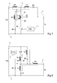
- the figure 5 represents an embodiment of a voltage converter according to the present invention.
- a fitting called freewheel, performing energy conversion without lowering or raising voltage.
- the inductor L0 directly connects a terminal 2 for applying the highest (for example positive) potential of a direct input voltage Vin and a terminal 3 for supplying a voltage Vs to a load (terminal 4 ' inductance L0 connected to terminal 3).
- the terminal 3 is also connected to an application terminal 5 of the lowest potential of the voltage Vin (for example, ground 5) by an inductive element L 'in series with a switching switch K.
- the switch K is controlled by a circuit 1 (CTRL).
- CTRL circuit 1
- the inductance L0 is a main winding of a magnetic circuit 10 comprising two secondary windings L1 and L2.
- a freewheeling diode DL in series with a first secondary winding L1 connects the terminals 2 and 3, the cathode of the diode DL being on the terminal side 2.
- a second secondary winding L2 in series with a diode D2 connects the terminals 3 and 5, the anode of the diode D2 being on the terminal side 5.
- the inductive element L ' is a mid-point inductor 30 connected by a diode D1 to terminal 2, the anode of the diode D1 being point side 30.
- This mid-point inductance forms, with the diode D1, a bi-value inductive element with automatic switching between its two values.
- the value of the inductance LA is chosen to be lower than that of the inductance LB.
- FIGS. 6A, 6B and 6C are chronograms illustrating the operation of the converter of the figure 5 .
- the Figure 6A is an example of the shape of the current IK in the switch K during a cutting cycle of the input voltage Vin.
- the Figures 6B and 6C represent the corresponding paces of the voltage VK across the switch K and the current ID1 in the diode D1.
- These gaits like those of the rest of the circuit, correspond to those of the Figures 2A to 2G but with a slope di / dt of growth of the current IK in the phase B and with a discharge (dIL '/ dt) of the inductive element L' fixed by values of inductances (LA and LA + LB) different.
- the equivalent diagram of the assembly amounts to applying the voltage Vin across the series connection of the inductance L0 with the inductance L '(LA + LB), the diodes DL, D1 and D2 being blocked.
- the current flowing through the inductance L0 is shared between the load (capacitor C0, figure 1 ) and the inductance L '.
- phase F the discharge of the control inductance L 'of the di / dt only takes place for a part of it (the inductance LA).
- the slope of this discharge therefore depends on the value of the inductance LA while the load gradient depends on the total value LA + LB.
- the figure 7 represents an embodiment of a boost converter. Compared to the assembly of the figure 1 the inductance L is replaced by an inductance L 'at the midpoint 30 and the anode of the diode D1 is connected to this midpoint. The operation of the circuit of the figure 7 can be deduced from the one exposed in relation to the previous montages.
- the figure 8 represents an embodiment of a down converter.
- the switch K connects the terminal 2 to a first end of the inductor L '(part side LA) and the inductance L0 is between the terminal 3 and the other end (terminal 4') of the inductor L ' .
- the series association of the diode DL and the inductor L1 is between the terminal 4 'and the ground 5, the anode of the diode DL being on the terminal side 5.
- the series association of the inductor L2 and the diode D2 connects the terminals 2 and 4 ', the anode of the diode D2 being on the terminal side 2.
- the diode D1 connects the midpoint 30 of the inductance L' to the ground 5, the anode of the diode D1 being mass side.
- circuits of figures 5 , 7 and 8 combine a soft switching reducing losses on closing the switch with recovery of some of these losses to reinject them into the load when the switch is open.
- Another advantage is that the operation is automatic in the change of value of the relevant inductance between the closing and opening of the switch.
- the operation of the circuit is compatible with high switching frequencies (more than a hundred kHz) and with powers greater than 0.5 kW.
- control circuit 1 provided that it regulates the output voltage Vs (which is usually the case), does not have to be modified to adapt the duty cycle.
- the magnetic circuit L0, L1, L2 can be realized as a single inductor with three windings.
- the inductive element L ' is preferably a mid-point inductor formed by a conductive winding on the same core. This has the advantage of avoiding possible problems of electromagnetic compatibility.
- the inductance L ' may consist of two separate windings in series.
- the automatic switching element of the value of the inductance between the closing (LA + LB) and opening (LB) phases is preferably a diode (D1) for its simplicity.
- a limiter represented by a dotted line in FIG. figure 5 (capacitor C in parallel with a resistor R, all in series with a diode D) between the switch K and the terminal 2 (with the cathode of the diode D side 2) in parallel on the diode D1.
- a similar arrangement can be provided between the switch K and the terminal 3 (with the cathode of the diode D on the terminal side 3) for a boost converter ( figure 7 ) or in parallel with the switch K (with the cathode of the diode D on the terminal side 2) for a down converter ( figure 8 ).
- the present invention is susceptible of various variations and modifications which will be apparent to those skilled in the art.
- the dimensions of the different windings of the magnetic circuit can be modified provided to respect a winding L0 of a number n0 of turns much higher (for example with a ratio of the order of 10) to the numbers n1 and n2 of turns of L1 and L2 windings.
- the numbers of turns of the windings L1 and L2 are equal.
- this choice depends for the value LA among others on the maximum frequency of cutting and the maximum power likely to be called by the load, and acceptable losses for the LB value.
- the LA and LB values are in a ratio (LB / LA) of between 0.1 and 0.7.
- the invention applies to any converter assembly (free-wheel, step-down, elevator or mixed) provided that it is a switching converter.
- the various mounting variants of the converters are transposable to the invention.
- inductance L0 into a (main) element of the magnetic circuit in series with a distinct inductance not belonging to the magnetic circuit. It will also be possible to adapt the switching speeds of the diodes although, in order to obtain the advantages of the invention, these diodes need not be fast.
Landscapes
- Engineering & Computer Science (AREA)
- Power Engineering (AREA)
- Dc-Dc Converters (AREA)
Abstract
L'invention concerne un convertisseur de puissance à découpage, comportant, entre une première extrémité (4) d'un élément inductif principal (L0) et un interrupteur (K), un élément inductif (L') bi-valeur (LA, LB) à commutation automatique entre ses deux valeurs.
Description
- La présente invention concerne le domaine des convertisseurs de puissance dits à découpage. De tels convertisseurs utilisent un élément inductif, associé à un interrupteur de puissance et à une diode de roue libre, pour effectuer une conversion d'énergie et une correction du facteur de puissance, généralement à partir d'une tension d'entrée continue. On connaît des convertisseurs abaisseurs de tension (BUCK), élévateurs de tension (BOOST) et mixtes (abaisseurs-élévateurs).
- La demande de brevet
US-A-2004/0113596 décrit un circuit d'aide à la commutation pour un convertisseur de puissance. Un circuit magnétique à plusieurs enroulements et à diodes de commutation sert à organiser la décharge d'une inductance de contrôle du di/dt à la fermeture de l'interrupteur de puissance du convertisseur et à stocker l'énergie lors de la commutation pour la transférer à la charge alimentée par le convertisseur. - La présente invention vise à pallier tout ou partie des inconvénients des convertisseurs à découpage.
- Un objet vise plus particulièrement une amélioration du principe utilisé par un circuit d'aide à la commutation à circuit magnétique organisant la décharge d'une inductance de contrôle du di/dt.
- Un objet vise également une solution compatible avec une utilisation du convertisseur à des fréquences de plusieurs centaines de kHz et pour des puissances de l'ordre du kW.
- Pour atteindre tout ou partie de ces objets ainsi que d'autres, il est prévu un convertisseur de puissance à découpage, comportant, entre une première extrémité d'un élément inductif principal et un interrupteur, un élément inductif bi-valeur à commutation automatique entre ses deux valeurs.
- Selon un mode de réalisation, l'élément inductif bi-valeur comporte deux éléments en série dont le point milieu est relié, par une première diode, à une borne d'application d'une tension d'entrée.
- Selon un mode de réalisation, l'élément inductif bi-valeur comporte deux éléments en série dont le point milieu est relié, par une première diode, à une borne de fourniture d'une tension de sortie.
- Selon un mode de réalisation, l'élément inductif bi-valeur est une inductance à point milieu.
- Selon un mode de réalisation, l'élément inductif principal forme un enroulement principal d'un circuit magnétique dont deux enroulements secondaires électriquement en série ont le point milieu de cette association en série relié à ladite première extrémité de l'enroulement inductif principal.
- Selon un mode de réalisation, chaque enroulement secondaire est en série avec une diode autre que la première diode.
- Selon un mode de réalisation, les enroulements secondaires participent à une décharge de l'élément inductif bi-valeur à l'ouverture et à la fermeture de l'interrupteur, l'un d'entres eux participant à un transfert de l'énergie correspondant à la fermeture audit enroulement principal.
- Ces objets, caractéristiques et avantages, ainsi que d'autres de la présente invention seront exposés en détail dans la description suivante de modes de réalisation particuliers faite à titre non-limitatif en relation avec les figures jointes parmi lesquelles :
- la
figure 1 représente un exemple de convertisseur élévateur de tension à circuit d'aide à la commutation usuel ; - les
figures 2A, 2B, 2C, 2D, 2E, 2F et 2G illustrent, sous forme de chronogrammes, le fonctionnement du convertisseur de lafigure 1 ; - les
figures 3A et 3B sont des agrandissements superposés des chronogrammes desfigures 2C et 2D pour deux valeurs d'inductance de contrôle du di/dt ; - les
figures 4A et 4B sont des extraits de lafigure 2F pour deux valeurs de puissance de sortie appellées par la charge ; - la
figure 5 représente un mode de réalisation d'un convertisseur de tension selon la présente invention ; - les
figures 6A, 6B et 6C illustrent, sous forme de chronogrammes, le fonctionnement du circuit de lafigure 5 ; - la
figure 7 représente un mode de réalisation d'un convertisseur élévateur de tension selon la présente invention; et - la
figure 8 représente un mode de réalisation d'un convertisseur abaisseur de tension selon la présente invention. - De mêmes éléments ont été désignés par de mêmes références aux différentes figures. Pour des raisons de clarté, seuls les éléments qui sont nécessaires à la compréhension de l'invention ont été représentés aux figures et seront décrits par la suite. En particulier, la constitution du circuit de commande de l'interrupteur de puissance n'a pas été détaillée, sa mise en oeuvre étant à la portée de l'homme du métier à partir des indications fonctionnelles données dans la présente description.
- La
figure 1 représente le schéma électrique d'un exemple de convertisseur à découpage élévateur de tension, équipé d'un circuit d'aide à la commutation usuel. - Le convertisseur de puissance comporte un interrupteur K commandé par un circuit 1 (CTRL), par exemple, un circuit de commande par modulation de largeur d'impulsions (PWM), par modulation de fréquence d'impulsions (FWM), etc. Une inductance d'accumulation d'énergie L0 est connectée, par une première borne, à une borne 2 d'application d'une tension d'entrée Vin (de son potentiel plus positif) fournie par une source non représentée (par exemple, continue ou alternative redressée). L'interrupteur K est en série avec une inductance L de contrôle du di/dt, reliée à la deuxième borne 4 de l'inductance L0. L'autre borne de l'interrupteur K est connectée à une deuxième borne 5 d'application de la tension d'entrée Vin (de son potentiel plus négatif, généralement un potentiel de référence, typiquement la masse). Une diode de roue libre DL est placée entre le point 4 et une borne positive 3 de sortie du convertisseur. Cette borne positive est connectée à une première électrode d'un condensateur de stockage C0 (le cas échéant faisant partie de la charge Q à alimenter) aux bornes duquel est présente la tension de sortie Vs. L'autre borne du condensateur C0 est reliée à la masse 5 et la cathode de la diode DL est côté borne 3.
- L'inductance L0 fait partie d'un circuit magnétique 10 dont elle constitue l'enroulement principal. Ce circuit magnétique 10 comprend deux enroulements secondaires L1 et L2 ayant des nombres de spires respectivement n1 et n2 inférieurs au nombre n0 de spires de l'inductance L0. Un premier enroulement L1 du circuit magnétique 10 est connecté en série avec la diode DL entre les bornes 3 et 4. Un deuxième enroulement L2 relie le point 4 à la borne 5 en étant associé en série à une diode D2, l'anode de la diode D2 étant dirigée vers la masse 5. Enfin, une diode D1 relie, à la borne 3, le point 12 entre l'inductance L et l'interrupteur K, l'anode de la diode D1 étant reliée au point 12.
- Le rôle de l'enroulement L1 est, à l'ouverture de l'interrupteur K, d'imposer une tension négative aux bornes de l'inductance L, de façon à lui permettre de transférer l'énergie qu'elle contient au condensateur C0. La diode D1 est alors polarisée en direct.
- L'enroulement L2 a pour rôle, lors de la fermeture de l'interrupteur K, d'imposer une tension négative aux bornes de l'inductance L, afin de transférer l'énergie qu'elle contient dans l'enroulement L2 du circuit magnétique 10. Cette énergie est récupérée par l'enroulement L0 qui la restitue au condensateur C0 lors de l'ouverture suivante de l'interrupteur.
- Pour respecter ces fonctionnalités, les points de phase respectifs des enroulements sont choisis de la façon suivante. En supposant le point de phase de l'enroulement L0 relié à la borne 2 comme cela est illustré en
figure 1 , le point de phase de l'enroulement L1 est côté point 4 et le point de phase de l'enroulement L2 est côté masse 5. Par contre, si le point de phase de l'enroulement L0 est connecté au point 4, le point de phase de l'enroulement L1 est côté borne 3 et le point de phase de l'enroulement L2 est côté point 4. Les positions des diodes DL et D2 par rapport aux enroulements L1 et L2 avec lesquels elles sont respectivement en série peuvent être inversées. - Pour réaliser un convertisseur abaisseur de tension, l'interrupteur K est connecté en série avec l'inductance L0 entre les bornes positives d'entrée 2 et de sortie 3 (ou entre la masse 5 et la borne 3) avec interposition de l'inductance L. La diode de roue libre DL en série avec l'enroulement L1 relie, à la masse (respectivement à la borne 2), le point milieu entre les inductances L et L0, l'anode de la diode DL étant reliée à la masse 5 (respectivement sa cathode étant reliée à la borne 2). L'inductance L2 en série avec la diode D2 est connectée entre la borne 2 et le point milieu entre les inductances L et L0 (respectivement entre ce point et la masse), l'anode de la diode D2 étant côté borne 2 (respectivement côté borne 5). Enfin, la diode D1 relie, à la masse 5 (respectivement à la borne 2), le point entre l'interrupteur K et l'inductance L, l'anode de la diode D1 étant reliée à la masse (respectivement sa cathode étant reliée à la borne 2). Avec une connexion de l'interrupteur K côté borne 2, si le point de phase de l'enroulement L0 est côté inductance L, le point de phase de l'enroulement L1 est côté borne de masse 5 et le point de phase de l'enroulement L2 est côté borne 2. Avec une connexion de l'interrupteur K côté masse, si le point de phase de l'enroulement L0 est côté borne 2, le point de phase de l'enroulement L1 est côté borne 3 et celui de l'enroulement L2 est côté masse 5.
- Le principe de fonctionnement est le même. De l'énergie est emmagasinée dans l'inductance L0 pendant les périodes de fermeture de l'interrupteur K. Pendant les périodes où l'interrupteur K est ouvert, cette énergie est restituée au condensateur C0, la diode de roue libre DL servant à reboucler le circuit et le circuit magnétique servant à récupérer des pertes liées à la commutation de fermeture de l'interrupteur de puissance pour les réinjecter dans la charge.
- Les
figures 2A à 2G représentent, sous forme de chronogrammes et sans respect d'échelle, un exemple de cycle de commutation de l'interrupteur K, illustrant le fonctionnement du circuit d'aide à la commutation représenté enfigure 1 . - La
figure 2A représente la tension VDL aux bornes de la diode de roue libre DL. Lafigure 2B représente le courant IDL dans la diode DL. Lafigure 2C représente la tension VK aux bornes de l'interrupteur K. Lafigure 2D représente le courant IK dans l'interrupteur. Lafigure 2E représente la tension VL aux bornes de l'inductance L de contrôle du di/dt. Lafigure 2F représente le courant ID1 dans la diode D1. Lafigure 2G représente le courant ID2 dans la diode D2. Les signes des courants et tensions représentés auxfigures 2A à 2G sont pris en relation avec les sens indiqués enfigure 1 . - On suppose qu'avant un instant t10, l'interrupteur K est ouvert, le convertisseur étant alors en roue libre (phase A). Pendant cette période de roue libre, un courant supposé constant 10 circule dans la diode DL en étant restitué par les inductances L0 et L1. Pendant cette phase A où l'interrupteur K est ouvert, le schéma équivalent du convertisseur comprend uniquement l'inductance L0 en série avec l'inductance L1 et la diode DL polarisée en direct entre les bornes 2 et 3 pour fournir l'énergie à la charge et au condensateur C0. La tension VDL aux bornes de cette diode est légèrement positive et correspond à la chute de tension dans la jonction PN en direct (de l'ordre de 0,7V). Côté interrupteur K, celui-ci voit à ses bornes une tension V0 correspondant à la tension Vs majorée de la tension VDL et diminuée de la chute de tension dans l'enroulement L1. La tension VL dans l'inductance L est en effet nulle dans cette période comme on le verra par la suite en relation avec la fin des chronogrammes. Les diodes D1 et D2 sont bloquées et les courants qui les traversent sont, par conséquent, nuls. Le courant IK dans l'interrupteur K ouvert est, bien entendu, nul.
- A l'instant t10, le circuit 1 commande la fermeture de l'interrupteur K. On entre donc dans une phase B (la première phase de la commutation) de début de fermeture. Du point de vue schéma équivalent et par rapport à la phase A, l'inductance L en série avec l'interrupteur K fermé (court-circuit) est intercalée entre le point 4 et la masse 5. Le di/dt à la fermeture de l'interrupteur K est essentiellement fonction de l'inductance L. En effet, ce di/dt dépend de la tension Vs, de la tension Vin, de la mutuelle inductance du circuit magnétique et des valeurs à vide L11 et L22 des inductances du transformateur constitué par les enroulements principal L0 et secondaires L1 et L2. En raison du rapport de spires choisi, la valeur L11 est très grande devant la valeur L22. La mutuelle inductance est par ailleurs faible devant la valeur L11. Il en découle que la pente (di/dt) est, en première approximation, égale à Vs/L. Le courant IDL dans la diode DL décroît donc avec cette pente jusqu'à un instant t12. Comme on a recours à une jonction PN, la diode présente une zone de charges recouvrées. Par conséquent, le courant IDL s'annule à un instant t11, intermédiaire entre les instants t10 et t12. Cet instant t11 correspond à l'instant où le courant dans le commutateur K atteint la valeur 10. Entre les instants t10 et t12, les diodes D1 et D2 restent bloquées. La tension VL aux bornes de l'inductance L devient approximativement égale à la tension Vs.
- A l'instant t12, le courant dans la diode DL atteint la valeur IRM correspondant au maximum de charges recouvrées. A partir de l'instant t12, les charges recouvrées par la diode DL diminuent. La diode DL se comporte alors comme une capacité. Comme le nombre de spires de l'inductance L1 est faible devant le nombre de spires de l'inductance L0, la tension VL1 à ses bornes est faible. Il en découle que la capacité constituée par la diode DL se charge en négatif. Ce phénomène est illustré en
figure 2B par une poursuite de la décroissance du courant IDL jusqu'à un instant t13 en forme de charge de capacité. Le courant décroît jusqu'à un courant Ir conditionné par l'inductance L2. En effet, la tension VL qui décroît pendant cette phase C devient négative jusqu'à rendre la diode D2 passante lorsque la tension VL devient suffisamment négative (instant t13). Côté diode DL, la tension VDL atteint, à l'instant t13, la valeur -(Vs + VL1 + VL2 + VD2). La tension VL atteint, à l'instant t13, la valeur -(VK + VL2 + VD2). - A l'instant t13 où la diode D2 devient passante, le courant IDL dans la diode DL s'interrompt brutalement et le courant correspondant est réinjecté dans l'inductance L2. Le courant en excès (Ir) donne l'amplitude maximale du courant dans l'inductance L2. Ce courant dépend des nombres de spires n0 et n2 des inductances L0 et L2. A partir de l'instant t13, on assiste à une conduction de la diode D2 (phase D). Comme la diode DL est bloquée, le condensateur C0 est déconnecté. Le circuit magnétique est, pendant la phase D, dissocié de la charge Q. La diode D2 sert alors d'élément de roue libre pour transférer l'énergie stockée par l'inductance L dans le circuit magnétique par l'intermédiaire de l'enroulement L2. Les tensions aux bornes de la diode DL et de l'inductance L restent inchangées. De même, l'interrupteur K étant fermé, la tension à ses bornes est nulle. La diode D1 est bloquée. Quand le courant est intégralement transféré dans le circuit magnétique par l'inductance L2, le courant dans celle-ci s'annule (instant t14), ce qui provoque le blocage naturel de la diode D2, c'est-à-dire avec un di/dt faible. L'enroulement L2 permet la décroissance du courant dans l'interrupteur K en transférant l'énergie au circuit magnétique qui le restituera par l'inductance L0. Entre les instants t13 et t14, le courant dans l'interrupteur K décroît depuis le niveau 10 + Ir jusqu'au niveau 10.
- A l'instant t14, la tension aux bornes de l'inductance L s'annule, l'énergie qu'elle contenait ayant été transférée dans le circuit magnétique. La tension aux bornes de la diode DL remonte légèrement tout en restant négative et prend une valeur -(Vs + VL1) + VL + VK. On se souviendra que les tensions VL et VK sont alors négligeables (considérées comme nulles) par rapport aux tensions Vs et VL1.
- A partir de l'instant t14, on entre dans une phase E où l'interrupteur K est fermé et où la commutation est terminée. Le schéma équivalent comprend uniquement la source de tension Vin, les inductances L0 et L, et l'interrupteur K. Le courant IK est stable au niveau 10 de même que la tension VDL, la diode de roue libre étant bloquée. La tension aux bornes de l'interrupteur K est, bien entendu, nulle de même que la tension aux bornes de l'inductance L et les courants dans les diodes D1 et D2. Pendant la phase E, l'inductance L0 se trouve chargée à travers l'inductance L et l'interrupteur K.
- A un instant t15 où le circuit 1 provoque l'ouverture de l'interrupteur K, on impose, grâce à la présence de l'enroulement L1, une tension négative aux bornes de l'inductance L. Dans ce cas, il n'est pas nécessaire de contrôler le di/dt à l'ouverture du transistor. Le courant s'interrompt brutalement dans l'interrupteur K. L'inversion de la tension aux bornes de l'inductance L1 provoque l'évacuation, par la diode D1, de l'énergie stockée pendant la phase E dans l'inductance L. A l'instant t15, le courant ID1 prend donc brusquement la valeur 10 et ce courant décroît jusqu'à s'annuler à un instant t16. La pente de décroissance du courant ID1 est fonction de la valeur de l'inductance L et correspond approximativement à VL1/L. Le courant dans l'inductance L s'annule à l'instant t16 et tout le courant accumulé dans l'enroulement L0 circule alors par l'enroulement L1 et la diode DL. On notera que les diodes DL et D1 conduisent en même temps, mais le courant dans la diode DL part de zéro à l'instant t15.
- A l'instant t16, on se retrouve dans la phase A où l'interrupteur est ouvert.
- Le recours à un circuit magnétique permet, entre autres, de récupérer des pertes liées à la commutation de fermeture de l'interrupteur de puissance pour les réinjecter dans la charge et, par ce biais, d'améliorer le rendement.
- Toutefois, son efficacité en terme de réduction des pertes est sensible d'une part à des variations de valeur de l'inductance L et d'autre part à des variations de la puissance appelée par la charge.
- Les
figures 3A et 3B sont des agrandissements superposés des chronogrammes desfigures 2C et 2D au début de la phase B (instant t10), c'est-à-dire d'un cycle de fermeture de l'interrupteur K, pour deux valeurs différentes de l'inductance L (respectivement inférieure et supérieure). - Alors que la pente de décroissance dVK/dt de la tension VK lors de la fermeture ne dépend pas de la valeur de l'inductance L, la pente di/dt d'établissement du courant IK dépend, entre autres, de cette valeur (di/dt = Vin/L). Il en résulte que plus la valeur de l'inductance L est faible (
figure 3B ), plus le courant atteint à travers l'interrupteur sous une tension non nulle (avant l'instant t20) est élevé. Comme l'intervalle de temps entre les instants t10 et t20 ne dépend pas de la valeur de L, plus la valeur de L est faible, plus la puissance dissipée dans l'interrupteur K à la fermeture est élevée (surface hachurée auxfigures 3A et 3B ). - Les
figures 4A et 4B reprennent le chronogramme de lafigure 2F (courant ID1 dans la diode D1) dans la phase F et autour pour deux puissances de sortie différentes (respectivement inférieure et supérieure), illustrant la décharge de l'inductance L dans la charge Q. - La pente de disparition du courant dépend de la tension aux bornes de l'inductance L, donc des tensions aux bornes des diodes D1 et DL et aux bornes de l'inductance L1 (dID1/dt = (-VL1+(VD1+VDL))/L), mais pas de la puissance appelée par la charge. Or, cette puissance conditionne la valeur du courant 10 traversant l'interrupteur K pendant la phase E, donc l'énergie que doit libérer l'inductance L pendant la phase F. Par conséquent, l'instant (t16 -
figure 4A , t16' -figure 4B ) auquel le courant ID1 s'annule et à partir duquel peut débuter le cycle suivant intervient de plus en plus tard avec une augmentation de la puissance. L'existence d'une phase A est cependant requise pour préserver les avantages d'une commutation douce qui requiert que l'inductance soit déchargée avant le début (instant t10) du cycle de commutation suivant. Il faut donc diminuer la valeur de l'inductance L (pour accélérer sa décharge en fin de cycle) si la puissance est plus élevée. - Il en est de même si la fréquence de découpage est élevée. En effet, en raccourcissant la durée globale du cycle (phases F à A), on dispose de moins de temps pour décharger l'inductance L et il faudrait donc en diminuer la valeur.
- Or, diminuer la valeur de l'inductance L engendre des pertes supérieures à la fermeture de l'interrupteur (
figures 3A et 3B ). De plus, les dispersions de valeurs liées aux tolérances de fabrications des enroulements inductifs des circuits magnétiques peuvent atteindre une vingtaine de pourcents. - On effectue donc généralement un compromis entre la puissance dissipée dans l'interrupteur à sa fermeture et la puissance et/ou la fréquence maximale de fonctionnement pour choisir la valeur de l'inductance L.
- Plus la fréquence ou la puissance est élevée, plus ce compromis est difficile. On perd alors les effets bénéfiques du contrôle du di/dt à la fermeture de l'interrupteur par l'inductance L.
- La
figure 5 représente un mode de réalisation d'un convertisseur de tension selon la présente invention. On suppose un montage, dit de roue libre, effectuant une conversion d'énergie sans abaissement ni élévation de tension. - Par rapport au montage de la
figure 1 , l'inductance L0 relie directement une borne 2 d'application du potentiel le plus élevé (par exemple positif) d'une tension continue d'entrée Vin et une borne 3 de fourniture d'une tension Vs à une charge (borne 4' de l'inductance L0 reliée à la borne 3). La borne 3 est également reliée à une borne 5 d'application du potentiel le plus faible de la tension Vin (par exemple, la masse 5) par un élément inductif L' en série avec un interrupteur de découpage K. L'interrupteur K est commandé par un circuit 1 (CTRL). L'inductance L0 est un enroulement principal d'un circuit magnétique 10 comportant deux enroulements secondaires L1 et L2. Une diode de roue libre DL en série avec un premier enroulement secondaire L1 relie les bornes 2 et 3, la cathode de la diode DL étant côté borne 2. Un deuxième enroulement secondaire L2 en série avec une diode D2 relie les bornes 3 et 5, l'anode de la diode D2 étant côté borne 5. Les positions des diodes DL et D2 par rapport aux enroulements L1 et L2 avec lesquels elles sont respectivement en série peuvent être inversées. - Selon ce mode de réalisation, l'élément inductif L' est une inductance à point milieu 30, relié par une diode D1 à la borne 2, l'anode de la diode D1 étant côté point 30. Cette inductance à point milieu forme, avec la diode D1, un élément inductif bi-valeur à commutation automatique entre ses deux valeurs.
- Fonctionnellement, cela revient à disposer deux inductances LA et LB en série entre l'inductance L0 et l'interrupteur K et à relier le point milieu 30 entre les inductances LA et LB à la borne 2 par la diode D1. La valeur de l'inductance LA est choisie pour être inférieure à celle de l'inductance LB.
- Les
figures 6A, 6B et 6C sont des chronogrammes illustrant le fonctionnement du convertisseur de lafigure 5 . Lafigure 6A est un exemple d'allure du courant IK dans l'interrupteur K pendant un cycle de découpage de la tension d'entrée Vin. Lesfigures 6B et 6C représentent les allures correspondantes de la tension VK aux bornes de l'interrupteur K et du courant ID1 dans la diode D1. Ces allures, comme celles du reste du circuit, correspondent à celles desfigures 2A à 2G , mais avec une pente di/dt de croissance du courant IK dans la phase B et avec une décharge (dIL'/dt) de l'élément inductif L' fixées par des valeurs d'inductances (LA et LA+LB) différentes. - Entre les instants t10 et t12, le schéma équivalent du montage revient à appliquer la tension Vin aux bornes de l'association en série de l'inductance L0 avec l'inductance L' (LA+LB), les diodes DL, D1 et D2 étant bloquées. Le courant traversant l'inductance L0 se partage entre la charge (condensateur C0,
figure 1 ) et l'inductance L'. - Entre les instants t15 et t16 (phase F), la décharge de l'inductance L' de contrôle du di/dt ne s'effectue que pour une partie de celle-ci (l'inductance LA). La pente de cette décharge dépend donc de la valeur de l'inductance LA alors que la pente de charge dépend de la valeur totale LA+LB. Cela permet de choisir la valeur de l'inductance LA en fonction de la durée souhaitée ou disponible pour la phase F et de préserver l'existence d'un temps mort (phase A) qui soit compatible avec les tolérances de fabrication, tout en préservant une inductance (LA+LB) suffisante pour une commutation douce à la fermeture de l'interrupteur.
- La
figure 7 représente un mode de réalisation d'un convertisseur élévateur. Par rapport au montage de lafigure 1 , l'inductance L est remplacée par une inductance L' à point milieu 30 et l'anode de la diode D1 est connectée à ce point milieu. Le fonctionnement du circuit de lafigure 7 se déduit de celui exposé en relation avec les montages précédents. - La
figure 8 représente un mode de réalisation d'un convertisseur abaisseur. Par rapport au montage de lafigure 7 , l'interrupteur K relie la borne 2 à une première extrémité de l'inductance L' (côté partie LA) et l'inductance L0 est entre la borne 3 et l'autre extrémité (borne 4') de l'inductance L'. L'association en série de la diode DL et de l'inductance L1 est entre la borne 4' et la masse 5, l'anode de la diode DL étant côté borne 5. L'association en série de l'inductance L2 et de la diode D2 relie les bornes 2 et 4', l'anode de la diode D2 étant côté borne 2. Enfin, la diode D1 relie le point milieu 30 de l'inductance L' à la masse 5, l'anode de la diode D1 étant côté masse. Le fonctionnement du circuit de lafigure 8 se déduit de celui exposé en relation avec les montages précédents. - Un avantage des circuits des
figures 5 ,7 et 8 est qu'ils combinent une commutation douce réduisant les pertes à la fermeture de l'interrupteur avec une récupération d'une partie de ces pertes pour les réinjecter dans la charge lorsque l'interrupteur est ouvert. - Un autre avantage est que le fonctionnement est automatique dans le changement de valeur de l'inductance concernée entre la fermeture et l'ouverture de l'interrupteur.
- Le fonctionnement du circuit est compatible avec des fréquences de découpage élevées (plus d'une centaine de kHz) et avec des puissances supérieures à 0,5 kW.
- De plus, aucune commande supplémentaire par rapport à celle habituelle de l'interrupteur à découpage K n'est nécessaire. En outre, le circuit de commande 1, pourvu qu'il effectue une régulation de la tension de sortie Vs (ce qui est généralement le cas), n'a pas à être modifié pour adapter le rapport cyclique.
- Le circuit magnétique L0, L1, L2 peut être réalisé sous la forme d'une seule inductance à trois enroulements.
- L'élément inductif L' est, de préférence, une inductance à point milieu réalisée par un enroulement conducteur sur un même noyau. Cela présente l'avantage d'éviter les éventuels problèmes de compatibilité électromagnétique. En variante, l'inductance L' pourra être constituée de deux enroulements distincts en série.
- L'élément de commutation automatique de la valeur de l'inductance entre les phases de fermeture (LA+LB) et d'ouverture (LB) est de préférence une diode (D1) pour sa simplicité.
- Pour éviter d'éventuelles surtensions aux bornes de l'interrupteur K, on peut optionnellement prévoir un limiteur représenté en pointillés en
figure 5 (condensateur C en parallèle avec une résistance R, le tout en série avec une diode D) entre l'interrupteur K et la borne 2 (avec la cathode de la diode D côté borne 2) en parallèle sur la diode D1. Un montage similaire peut être prévu, entre l'interrupteur K et la borne 3 (avec la cathode de la diode D côté borne 3) pour un convertisseur élévateur (figure 7 ) ou en parallèle avec l'interrupteur K (avec la cathode de la diode D côté borne 2) pour un convertisseur abaisseur (figure 8 ). - Bien entendu, la présente invention est susceptible de diverses variantes et modifications qui apparaîtront à l'homme de l'art. En particulier, les dimensionnements des différents enroulements du circuit magnétique pourront être modifiés pourvu de respecter un enroulement L0 d'un nombre n0 de spires nettement supérieur (par exemple avec un rapport de l'ordre de 10) aux nombres n1 et n2 de spires des enroulements L1 et L2. De préférence, les nombres de spires des enroulements L1 et L2 sont égaux. Pour l'inductance L', ce choix dépend pour la valeur LA entre autres de la fréquence maximale de découpage et de la puissance maximale susceptible d'être appelée par la charge, et des pertes acceptables pour la valeur LB. Par exemple, les valeurs LA et LB sont dans un rapport (LB/LA) compris entre 0,1 et 0,7.
- De plus, l'invention s'applique à tout montage de convertisseur (roue-libre, abaisseur, élévateur ou mixte) pourvu qu'il s'agisse d'un convertisseur à découpage. En particulier, les diverses variantes de montage des convertisseurs (interrupteur K côté borne plus positive 2 ou plus négative 5, positions respectives des diodes dans leurs associations en série avec les inductances, etc.) sont transposables à l'invention.
- Enfin, parmi les variantes possibles, on pourra diviser l'inductance L0 en un élément (principal) du circuit magnétique en série avec une inductance distincte n'appartenant pas au circuit magnétique. On pourra également adapter les vitesses de commutation des diodes bien que, pour obtenir les avantages de l'invention, ces diodes n'aient pas besoin d'être rapides.
Claims (7)
- Convertisseur de puissance à découpage, caractérisé en ce qu'il comporte, entre une première extrémité (4, 4') d'un élément inductif principal (L0) et un interrupteur (K), un élément inductif (L') bi-valeur (LA, LB) à commutation automatique entre ses deux valeurs, formé de deux éléments inductifs en série et d'un élément de commutation automatique.
- Convertisseur selon la revendication 1, dans lequel l'élément inductif bi-valeur (L') comporte deux éléments en série dont le point milieu (30) est relié, par une première diode (D1), à une borne (2, 5) d'application d'une tension d'entrée (Vin).
- Convertisseur selon la revendication 1, dans lequel l'élément inductif bi-valeur (L') comporte deux éléments en série dont le point milieu (30) est relié, par une première diode (D1), à une borne (3) de fourniture d'une tension de sortie (Vs).
- Convertisseur selon l'une quelconque des revendications 1 à 3, dans lequel l'élément inductif bi-valeur (L') est une inductance à point milieu (30).
- Convertisseur selon l'une quelconque des revendications 1 à 4, dans lequel l'élément inductif principal (L0) forme un enroulement principal d'un circuit magnétique (10) dont deux enroulements secondaires (L1, L2) électriquement en série ont le point milieu de cette association en série relié à ladite première extrémité (4, 4') de l'enroulement inductif principal.
- Convertisseur selon la revendication 5, dans lequel chaque enroulement secondaire (L1, L2) est en série avec une diode (DL, D2) autre que la première diode (D1).
- Convertisseur selon la revendication 5 ou 6, dans lequel les enroulements secondaires (L1, L2) participent à une décharge de l'élément inductif bi-valeur (L') à l'ouverture et à la fermeture de l'interrupteur (K), l'un d'entre eux participant à un transfert de l'énergie correspondant à la fermeture audit enroulement principal (L0).
Applications Claiming Priority (1)
| Application Number | Priority Date | Filing Date | Title |
|---|---|---|---|
| FR0753026 | 2007-02-02 |
Publications (1)
| Publication Number | Publication Date |
|---|---|
| EP1953904A1 true EP1953904A1 (fr) | 2008-08-06 |
Family
ID=38421601
Family Applications (1)
| Application Number | Title | Priority Date | Filing Date |
|---|---|---|---|
| EP08101205A Withdrawn EP1953904A1 (fr) | 2007-02-02 | 2008-02-01 | Circuit d'aide à la commutation pour un convertisseur à découpage |
Country Status (2)
| Country | Link |
|---|---|
| US (1) | US7768243B2 (fr) |
| EP (1) | EP1953904A1 (fr) |
Cited By (1)
| Publication number | Priority date | Publication date | Assignee | Title |
|---|---|---|---|---|
| FR3104343A1 (fr) * | 2019-12-06 | 2021-06-11 | Valeo Siemens eAutomotive France | Dispositif de correction de facteur de puissance et système électrique comportant un tel dispositif |
Families Citing this family (5)
| Publication number | Priority date | Publication date | Assignee | Title |
|---|---|---|---|---|
| EP2230754B1 (fr) * | 2009-03-18 | 2015-04-29 | STMicroelectronics (Tours) SAS | Alimentation à découpage |
| US8525450B2 (en) * | 2010-03-29 | 2013-09-03 | Regal Beloit America, Inc. | Power factor correction drive circuit topologies and control for switched reluctance machines |
| GB2532454A (en) * | 2014-11-19 | 2016-05-25 | Univ Plymouth | Control arrangement |
| CN109149925B (zh) * | 2018-09-21 | 2019-10-22 | 广东工业大学 | 一种降压斩波电路 |
| CN115765447B (zh) * | 2022-11-08 | 2023-06-02 | 东北电力大学 | 一种双耦合电感串联型直流升压变换器及控制方法 |
Citations (4)
| Publication number | Priority date | Publication date | Assignee | Title |
|---|---|---|---|---|
| JPS6070967A (ja) * | 1983-09-27 | 1985-04-22 | Mitsubishi Electric Corp | 直流電源回路 |
| EP0910158A1 (fr) * | 1997-02-10 | 1999-04-21 | TDK Corporation | Alimentation a decoupage et a elevation de tension |
| US6028418A (en) * | 1999-02-11 | 2000-02-22 | Delta Electronics, Inc. | Boost converter with minimum-component-count active snubber |
| WO2002073783A2 (fr) * | 2001-03-09 | 2002-09-19 | Stmicroelectronics S.A. | Circuit d'aide a la commutation d'un convertisseur a decoupage |
Family Cites Families (4)
| Publication number | Priority date | Publication date | Assignee | Title |
|---|---|---|---|---|
| GB8816774D0 (en) * | 1988-07-14 | 1988-08-17 | Bsr Int Plc | Power supplies |
| US5307004A (en) * | 1992-07-06 | 1994-04-26 | Carsten Bruce W | Soft switching boost and buck regulators |
| US5481238A (en) * | 1994-04-19 | 1996-01-02 | Argus Technologies Ltd. | Compound inductors for use in switching regulators |
| US6507174B1 (en) * | 2001-09-06 | 2003-01-14 | Koninklijke Philips Electronics N.V. | Voltage regulator with clamping circuit |
-
2008
- 2008-01-31 US US12/023,333 patent/US7768243B2/en not_active Expired - Fee Related
- 2008-02-01 EP EP08101205A patent/EP1953904A1/fr not_active Withdrawn
Patent Citations (5)
| Publication number | Priority date | Publication date | Assignee | Title |
|---|---|---|---|---|
| JPS6070967A (ja) * | 1983-09-27 | 1985-04-22 | Mitsubishi Electric Corp | 直流電源回路 |
| EP0910158A1 (fr) * | 1997-02-10 | 1999-04-21 | TDK Corporation | Alimentation a decoupage et a elevation de tension |
| US6028418A (en) * | 1999-02-11 | 2000-02-22 | Delta Electronics, Inc. | Boost converter with minimum-component-count active snubber |
| WO2002073783A2 (fr) * | 2001-03-09 | 2002-09-19 | Stmicroelectronics S.A. | Circuit d'aide a la commutation d'un convertisseur a decoupage |
| US20040113596A1 (en) | 2001-03-09 | 2004-06-17 | Benoit Peron | Auxiliary switching circuit for a chopping converter |
Cited By (1)
| Publication number | Priority date | Publication date | Assignee | Title |
|---|---|---|---|---|
| FR3104343A1 (fr) * | 2019-12-06 | 2021-06-11 | Valeo Siemens eAutomotive France | Dispositif de correction de facteur de puissance et système électrique comportant un tel dispositif |
Also Published As
| Publication number | Publication date |
|---|---|
| US7768243B2 (en) | 2010-08-03 |
| US20080186748A1 (en) | 2008-08-07 |
Similar Documents
| Publication | Publication Date | Title |
|---|---|---|
| FR2821996A1 (fr) | Circuit a la commutation d'un convertisseur a decoupage | |
| EP2230754B1 (fr) | Alimentation à découpage | |
| FR3097089A1 (fr) | Un convertisseur et son systeme de controle de courant | |
| EP2599206A2 (fr) | Convertisseur dc/dc quadratique double boost bidirectionnel en courant | |
| FR3001089A1 (fr) | Equilibrage de charge dans une batterie electrique | |
| EP2258036B1 (fr) | Dispositif de commande d'une alimentation a decoupage dc dc, du type a n voies entrelacees | |
| EP2258037A1 (fr) | Alimentation a decoupage dc dc non isolee | |
| EP2320553B1 (fr) | Dispositif convertisseur et alimentation sans interruption équipée d'un tel dispositif | |
| FR2956260A1 (fr) | Systeme d'equilibrage de charge pour batteries | |
| EP3079247B1 (fr) | Circuit de commande d'un pont redresseur | |
| FR2923962A1 (fr) | Circuit elevateur de tension | |
| EP1101276B1 (fr) | Circuit de conversion dc/dc | |
| WO1999034501A1 (fr) | Procede de commande d'un convertisseur de tension continu-continu a stockage inductif | |
| EP1704634A1 (fr) | Gestion du court-circuit dans une inductance d un convertiss eur elevateur de tension | |
| EP4115512A1 (fr) | Procédé et dispositif de conversion d'une tension avec commutation douce des interrupteurs | |
| EP1528661B1 (fr) | Circuit de commande d'un transistor MOS pour redresseur synchrone | |
| EP3721543A1 (fr) | Convertisseur continu-continu avec pre-charge d'un premier reseau electrique a partir d'un deuxieme reseau electrique | |
| EP2781023B1 (fr) | Variateur de puissance | |
| EP3584918B1 (fr) | Convertisseur à découpage | |
| EP0147306A2 (fr) | Amplificateur de puissance linéaire | |
| FR2698499A1 (fr) | Circuit pour faire fonctionner une charge inductive. | |
| EP0966092A1 (fr) | Convertisseur courant continu-courant continu | |
| EP3195459B1 (fr) | Convertisseur de tension continue et procédé de commande associé | |
| FR3151162A1 (fr) | Circuit de conversion d'alimentation DC/DC | |
| FR2922694A1 (fr) | Procede de commande d'une alimentation de decoupage et alimentation correspondante |
Legal Events
| Date | Code | Title | Description |
|---|---|---|---|
| PUAI | Public reference made under article 153(3) epc to a published international application that has entered the european phase |
Free format text: ORIGINAL CODE: 0009012 |
|
| AK | Designated contracting states |
Kind code of ref document: A1 Designated state(s): AT BE BG CH CY CZ DE DK EE ES FI FR GB GR HR HU IE IS IT LI LT LU LV MC MT NL NO PL PT RO SE SI SK TR |
|
| AX | Request for extension of the european patent |
Extension state: AL BA MK RS |
|
| AKX | Designation fees paid | ||
| REG | Reference to a national code |
Ref country code: DE Ref legal event code: 8566 |
|
| STAA | Information on the status of an ep patent application or granted ep patent |
Free format text: STATUS: THE APPLICATION IS DEEMED TO BE WITHDRAWN |
|
| 18D | Application deemed to be withdrawn |
Effective date: 20090207 |