EP1953116A2 - Microsystème d'actionnement et procédé de fabrication associé - Google Patents
Microsystème d'actionnement et procédé de fabrication associé Download PDFInfo
- Publication number
- EP1953116A2 EP1953116A2 EP20080354005 EP08354005A EP1953116A2 EP 1953116 A2 EP1953116 A2 EP 1953116A2 EP 20080354005 EP20080354005 EP 20080354005 EP 08354005 A EP08354005 A EP 08354005A EP 1953116 A2 EP1953116 A2 EP 1953116A2
- Authority
- EP
- European Patent Office
- Prior art keywords
- pivoting arm
- layer
- microsystem
- contact pad
- hinge
- Prior art date
- Legal status (The legal status is an assumption and is not a legal conclusion. Google has not performed a legal analysis and makes no representation as to the accuracy of the status listed.)
- Withdrawn
Links
- 238000004519 manufacturing process Methods 0.000 title claims description 36
- 230000004913 activation Effects 0.000 title 1
- 239000000758 substrate Substances 0.000 claims abstract description 34
- NJPPVKZQTLUDBO-UHFFFAOYSA-N novaluron Chemical compound C1=C(Cl)C(OC(F)(F)C(OC(F)(F)F)F)=CC=C1NC(=O)NC(=O)C1=C(F)C=CC=C1F NJPPVKZQTLUDBO-UHFFFAOYSA-N 0.000 claims abstract description 16
- PXHVJJICTQNCMI-UHFFFAOYSA-N Nickel Chemical compound [Ni] PXHVJJICTQNCMI-UHFFFAOYSA-N 0.000 claims description 26
- 239000000463 material Substances 0.000 claims description 16
- XEEYBQQBJWHFJM-UHFFFAOYSA-N Iron Chemical compound [Fe] XEEYBQQBJWHFJM-UHFFFAOYSA-N 0.000 claims description 12
- 229910052759 nickel Inorganic materials 0.000 claims description 10
- 229910000990 Ni alloy Inorganic materials 0.000 claims description 9
- 238000000151 deposition Methods 0.000 claims description 9
- 230000015572 biosynthetic process Effects 0.000 claims description 6
- 230000008021 deposition Effects 0.000 claims description 6
- 238000005530 etching Methods 0.000 claims description 6
- 229910052581 Si3N4 Inorganic materials 0.000 claims description 4
- 229910052751 metal Inorganic materials 0.000 claims description 4
- 239000002184 metal Substances 0.000 claims description 4
- HQVNEWCFYHHQES-UHFFFAOYSA-N silicon nitride Chemical compound N12[Si]34N5[Si]62N3[Si]51N64 HQVNEWCFYHHQES-UHFFFAOYSA-N 0.000 claims description 4
- UMIVXZPTRXBADB-UHFFFAOYSA-N benzocyclobutene Chemical compound C1=CC=C2CCC2=C1 UMIVXZPTRXBADB-UHFFFAOYSA-N 0.000 claims description 3
- 239000003302 ferromagnetic material Substances 0.000 claims description 3
- 229910052742 iron Inorganic materials 0.000 claims description 3
- 229920000642 polymer Polymers 0.000 claims description 3
- ZOKXTWBITQBERF-UHFFFAOYSA-N Molybdenum Chemical compound [Mo] ZOKXTWBITQBERF-UHFFFAOYSA-N 0.000 claims description 2
- 230000008030 elimination Effects 0.000 claims description 2
- 238000003379 elimination reaction Methods 0.000 claims description 2
- 229910052750 molybdenum Inorganic materials 0.000 claims description 2
- 239000011733 molybdenum Substances 0.000 claims description 2
- 230000035882 stress Effects 0.000 description 10
- PCHJSUWPFVWCPO-UHFFFAOYSA-N gold Chemical compound [Au] PCHJSUWPFVWCPO-UHFFFAOYSA-N 0.000 description 9
- 239000010931 gold Substances 0.000 description 8
- 238000000034 method Methods 0.000 description 8
- VYZAMTAEIAYCRO-UHFFFAOYSA-N Chromium Chemical compound [Cr] VYZAMTAEIAYCRO-UHFFFAOYSA-N 0.000 description 7
- 229910052737 gold Inorganic materials 0.000 description 7
- 239000011651 chromium Substances 0.000 description 6
- 230000008901 benefit Effects 0.000 description 5
- 229910052804 chromium Inorganic materials 0.000 description 5
- 238000004377 microelectronic Methods 0.000 description 5
- 229910000640 Fe alloy Inorganic materials 0.000 description 4
- KRHYYFGTRYWZRS-UHFFFAOYSA-N Fluorane Chemical compound F KRHYYFGTRYWZRS-UHFFFAOYSA-N 0.000 description 4
- 238000000623 plasma-assisted chemical vapour deposition Methods 0.000 description 4
- 229910000599 Cr alloy Inorganic materials 0.000 description 3
- 230000010354 integration Effects 0.000 description 3
- 235000001674 Agaricus brunnescens Nutrition 0.000 description 2
- 229910001020 Au alloy Inorganic materials 0.000 description 2
- VYPSYNLAJGMNEJ-UHFFFAOYSA-N Silicium dioxide Chemical compound O=[Si]=O VYPSYNLAJGMNEJ-UHFFFAOYSA-N 0.000 description 2
- XUIMIQQOPSSXEZ-UHFFFAOYSA-N Silicon Chemical compound [Si] XUIMIQQOPSSXEZ-UHFFFAOYSA-N 0.000 description 2
- 229910045601 alloy Inorganic materials 0.000 description 2
- 239000000956 alloy Substances 0.000 description 2
- 230000000903 blocking effect Effects 0.000 description 2
- 239000000788 chromium alloy Substances 0.000 description 2
- 238000007796 conventional method Methods 0.000 description 2
- 230000005291 magnetic effect Effects 0.000 description 2
- 230000007246 mechanism Effects 0.000 description 2
- 229920002120 photoresistant polymer Polymers 0.000 description 2
- BASFCYQUMIYNBI-UHFFFAOYSA-N platinum Chemical compound [Pt] BASFCYQUMIYNBI-UHFFFAOYSA-N 0.000 description 2
- 230000008569 process Effects 0.000 description 2
- 229910052710 silicon Inorganic materials 0.000 description 2
- 239000010703 silicon Substances 0.000 description 2
- 229910052814 silicon oxide Inorganic materials 0.000 description 2
- 229910000838 Al alloy Inorganic materials 0.000 description 1
- 229910001030 Iron–nickel alloy Inorganic materials 0.000 description 1
- KJTLSVCANCCWHF-UHFFFAOYSA-N Ruthenium Chemical compound [Ru] KJTLSVCANCCWHF-UHFFFAOYSA-N 0.000 description 1
- 229910004298 SiO 2 Inorganic materials 0.000 description 1
- 230000002411 adverse Effects 0.000 description 1
- 230000032683 aging Effects 0.000 description 1
- 238000005452 bending Methods 0.000 description 1
- 230000008859 change Effects 0.000 description 1
- 239000004020 conductor Substances 0.000 description 1
- 238000006073 displacement reaction Methods 0.000 description 1
- 230000000694 effects Effects 0.000 description 1
- 239000003353 gold alloy Substances 0.000 description 1
- 239000011810 insulating material Substances 0.000 description 1
- 239000007769 metal material Substances 0.000 description 1
- 150000004767 nitrides Chemical class 0.000 description 1
- 229910052697 platinum Inorganic materials 0.000 description 1
- 238000003825 pressing Methods 0.000 description 1
- 230000000750 progressive effect Effects 0.000 description 1
- 230000009467 reduction Effects 0.000 description 1
- 229910052707 ruthenium Inorganic materials 0.000 description 1
- 239000004065 semiconductor Substances 0.000 description 1
- 238000004088 simulation Methods 0.000 description 1
- 238000004513 sizing Methods 0.000 description 1
Images



Classifications
-
- B—PERFORMING OPERATIONS; TRANSPORTING
- B81—MICROSTRUCTURAL TECHNOLOGY
- B81B—MICROSTRUCTURAL DEVICES OR SYSTEMS, e.g. MICROMECHANICAL DEVICES
- B81B3/00—Devices comprising flexible or deformable elements, e.g. comprising elastic tongues or membranes
- B81B3/0035—Constitution or structural means for controlling the movement of the flexible or deformable elements
- B81B3/0051—For defining the movement, i.e. structures that guide or limit the movement of an element
-
- H—ELECTRICITY
- H01—ELECTRIC ELEMENTS
- H01H—ELECTRIC SWITCHES; RELAYS; SELECTORS; EMERGENCY PROTECTIVE DEVICES
- H01H1/00—Contacts
- H01H1/0036—Switches making use of microelectromechanical systems [MEMS]
-
- H—ELECTRICITY
- H01—ELECTRIC ELEMENTS
- H01H—ELECTRIC SWITCHES; RELAYS; SELECTORS; EMERGENCY PROTECTIVE DEVICES
- H01H36/00—Switches actuated by change of magnetic field or of electric field, e.g. by change of relative position of magnet and switch, by shielding
- H01H36/0006—Permanent magnet actuating reed switches
- H01H36/0013—Permanent magnet actuating reed switches characterised by the co-operation between reed switch and permanent magnet; Magnetic circuits
-
- H—ELECTRICITY
- H01—ELECTRIC ELEMENTS
- H01H—ELECTRIC SWITCHES; RELAYS; SELECTORS; EMERGENCY PROTECTIVE DEVICES
- H01H50/00—Details of electromagnetic relays
- H01H50/005—Details of electromagnetic relays using micromechanics
-
- H—ELECTRICITY
- H01—ELECTRIC ELEMENTS
- H01H—ELECTRIC SWITCHES; RELAYS; SELECTORS; EMERGENCY PROTECTIVE DEVICES
- H01H59/00—Electrostatic relays; Electro-adhesion relays
- H01H59/0009—Electrostatic relays; Electro-adhesion relays making use of micromechanics
-
- Y—GENERAL TAGGING OF NEW TECHNOLOGICAL DEVELOPMENTS; GENERAL TAGGING OF CROSS-SECTIONAL TECHNOLOGIES SPANNING OVER SEVERAL SECTIONS OF THE IPC; TECHNICAL SUBJECTS COVERED BY FORMER USPC CROSS-REFERENCE ART COLLECTIONS [XRACs] AND DIGESTS
- Y10—TECHNICAL SUBJECTS COVERED BY FORMER USPC
- Y10T—TECHNICAL SUBJECTS COVERED BY FORMER US CLASSIFICATION
- Y10T29/00—Metal working
- Y10T29/49—Method of mechanical manufacture
- Y10T29/49002—Electrical device making
- Y10T29/49105—Switch making
Definitions
- the invention also relates to a method of manufacturing such a microsystem.
- Patent applications US 2003/0173957 and US 2005/0083156 and the patent US 6,750,745 each describe an operating microsystem, more particularly an electrical circuit switch device, by means of a movable magnetic element.
- Such devices are manufactured by means of microelectronics processes giving a good integration capacity, thus aiming at lowering manufacturing costs while preserving a good control of the manufacturing.
- such an actuating microsystem 1 is produced on a plane substrate 2 and comprises a pivoting arm 3, rotatably mounted and hinged about a hinge 4, supported by the substrate 2.
- the pivoting arm 3 is actuated, for example, by a vertical magnetic force F, oriented upwards perpendicular to the substrate 2, and comprises a movable contact pad 5, integral with the lower face of the pivoting arm 3, intended to come into contact with a stud fixed contact 6, made on the upper surface of the substrate 2.
- the aim of the invention is to remedy all of the aforementioned disadvantages and to provide an actuating microsystem comprising an end stop for opening a pivoting arm, which is effective, and which does not alter the operation of the microsystem, and which allows to control the rotation of the pivoting arm.
- the invention also relates to a method for producing such a microsystem, which is simple, fast and economical.
- the actuating microsystem 1 comprises the pivoting arm 3, for example in the form of a plate having two longitudinal edges 3a and 3b, rotatably mounted around the hinge 4 at a hinge end 3c.
- the pivoting arm 3 comprises, for example, two movable contact pads 5, placed at a free end 3d of the pivoting arm 3, opposite the articulation end 3c, integral with the lower surface of the pivoting arm 3 and intended to cooperate with, for example, two fixed contact pads 6, made on the upper surface of the substrate 2.
- the microsystem 1 comprises, for example, two end stops 7a, 7b opening the pivoting arm 3 ( figure 2 ), formed on the substrate, arranged on either side of the pivoting arm 3 and on which the longitudinal edges 3a, 3b of the pivoting arm 3 abut, respectively, in order to block the rotation of the pivoting arm 3.
- the limit stop 7 comprises a foot 8 and a head 9, defining a substantially mushroom-shaped stop protruding at least partially above the corresponding longitudinal edge 3a, 3b of the pivoting arm 3.
- the foot 8 of the 7 is disposed between the hinge 4 and the fixed contact pad 6, made on the substrate 2 (FIG. figure 2 ), and the foot 8 consists of three parts.
- the first part of the foot 8 is a support pad 10, formed on the substrate 2 and, preferably, in the same material as the hinge 4, in particular any material that does not degrade during the release by etching of the pivoting arm 3 during the manufacturing process as described below.
- the second part of the foot 8 is a pedestal 11, extending the support pad 10 and preferably formed in the same material as the pivoting arm 3.
- the third part of the foot 8 is a support portion 12 of the head 9, formed preferably in the same material as the head 9.
- the head 9 of the limit stop 7 is, for example, curved, to define substantially the characteristic shape of a mushroom cap, and protrudes above the associated longitudinal edge 3a, 3b of the pivoting arm 3, so as to to block the rotation of the pivoting arm 3 and thus serve as a limit stop, for the opening of the pivoting arm 3.
- the characteristic mushroom shape of the head 9 of the limit stop 7 is obtained advantageously by electrolytic deposition of a material compatible with this type of process, especially any metallic material, capable of withstanding the etching steps for the release of the microsystem as described below.
- the head 9 and the support portion 12 of the head 9 are made of iron, nickel, gold, chromium or any alloy comprising at least two of these materials.
- the support portion 12 of the head 9 has a thickness of the order of 1 ⁇ m to 5 ⁇ m .
- the pivoting arm 3 is composed of a layer of ferromagnetic material, for example an alloy of nickel and iron, and has a thickness of the order of 5 .mu.m to 10 .mu.m .
- the support pad 10 and the hinge 4 are made of chromium, nickel, gold or chromium alloy and nickel, nickel alloy and gold or, preferably, chromium alloy, nickel and gold.
- the head 9 of the abutment 7 is, for example, curved, circular and has a diameter greater than the width of the support portion 12 by a distance d of the order of 2 microns .
- Such dimensions thus make it possible to determine a predetermined opening angle for the pivoting arm 3, for its rotation around the hinge 4, until it comes into abutment against the head 9 of the limit stop 7 ( figure 3 ).
- a manufacturing method according to the invention of the microsystem 1, as represented on the Figures 2 and 3 will be described in more detail with regard to Figures 4 to 8 .
- the method comprises, in a first step, the formation of the fixed contact pads 6 on the upper surface of the substrate 2, then, in a second step, the preferably simultaneous formation of the hinge 4 and the support pads 10 of the feet 8 end stops 7 ( figure 3 ).
- the support pads 10 are formed between the hinge 4 and the fixed contact pads 6, by structuring a first layer of the same material, for example chromium, nickel, gold or aluminum alloy. chromium and nickel, deposited on the substrate 2 and the fixed contact pads 6 previously formed.
- a sacrificial layer 13 for example made of silicon oxide (SiO 2 ), formed, for example, by a plasma-enhanced chemical vapor deposition (commonly known as "Plasma Enhanced Chemical Vapor Deposition” or PECVD) is then formed in a third step, around the hinge 4, support pads 10 and fixed contact pads 6.
- a conductive layer for example gold, nickel, chromium, platinum or ruthenium , of thickness of the order of 0.1 ⁇ m to 1 ⁇ m , is then deposited on the sacrificial layer 13, so as to form at least one movable contact pad 5 on the lower surface of the pivoting arm 3, to come into contact with the associated fixed contact pads 6.
- the method then comprises forming the pivoting arm 3 in a second layer, for example made of nickel and iron alloy, from a conductive layer 14, for example made of nickel, gold or alloy of nickel and iron, of thickness of the order of 0.1 .mu.m , deposited on the sacrificial layer 13 and structured to allow deposition including electrolytic growth.
- the fifth step consists in depositing a photoresist mask 15, for example with a thickness of the order of 5 ⁇ m to 10 ⁇ m , on the conductive layer 14, the mask 15 being partially open in the predetermined form.
- the pivoting arm 3 and the pedestal 11 of the foot 8 of the limit stop 7 are formed, advantageously simultaneously, for example, by electrolytic deposition of a layer of nickel alloy and iron.
- the conductive layer 14 is advantageously etched in the desired shape, via a mask ( figure 5 ), in order to maintain electrical contact for the pedestal 11.
- a mask 16 for example in photoresist, is deposited on the pivoting arm 3 and the pedestal 11.
- the mask 16 is then etched, so as to form an opening 17 at Pedestal 11 ( figure 6 ).
- a third layer for example of nickel-iron alloy, is then deposited, for example, by electrolytic deposition first up to the upper limit of the mask 16, to form the support portion 12 of the head 9 constituting the third part of the foot 8 of the abutment 7, and then by overflow of the material above the pivoting arm 3, to form the head 9 of the limit stop 7.
- the mask 16 is then eliminated, for example by etching ( figure 7 ), and the remainder of the conductive layer 14 is then removed also by etching.
- the sacrificial layer 13 is removed, for example by etching with hydrofluoric acid, in order to release the pivoting arm 3.
- a microsystem 1 as shown schematically on the Figures 2, 3 and 8 is thus obtained, with the manufacture of limit stops 7 made in a simple manner by conventional manufacturing steps in microelectronics, integrated in the manufacturing steps of the microsystem 1 itself. This results in a gain in terms of time and especially in terms of manufacturing costs.
- the actuating microsystem 1 according to the invention differs from the microsystem 1 represented on the Figures 2 to 8 by the shape of the limit stop 7 for opening the pivoting arm 3.
- the limit stop 7 is U-shaped, defining substantially a gantry having two lateral branches 18 under stress, connected by a transverse branch 19, which may be in the same material or in a material different from the lateral branches 18. More particularly, the transverse branch 19 is of any insulating, semiconducting or conductive material which is not soluble in hydrofluoric acid, for example silicon nitride, silicon, nickel, chromium, gold or any alloy with base of nickel, chrome and gold.
- under stress means that at least the lateral branches 18 of the limit stop 7 are composed of layers of different materials, that is to say having different coefficients of thermal expansion or stress states. different. This results in their deformation after relaxation of the stresses, allowing them in particular to take a substantially raised position at rest ( figures 10 and 13 ), as described in particular in the article “Effect of width on the stress-induced bending of micromachined bilayer cantilevers” by Max Ti-Kuang Hou et al. (J. Micromech Microeng 13 (2003) pp.141-148 ) and in the article “Curled micro-cantilevers using benzocyclobutene polymer and Mo for wafer level probing" by Si-Hyung Lee et al. (Sensors and Actuators A 121 (2005) pp.472-479 ).
- the side branches 18 are disposed on either side of the pivoting arm 3, parallel to the longitudinal edges 3a, 3b, and have a first end connected to the substrate 2 by a corresponding support pad 20 and a second end connected to the branch 19.
- the support pads 20 are arranged laterally with respect to the pivoting arm 3 (FIG. figure 9 ), between the hinge 4 and the fixed contact pads 6, and the lateral branches 18 of the limit stop 7 are oriented so that the transverse branch 19 is situated opposite the hinge 4 ( figure 10 ).
- the lateral branches 18 are bent upwards ( figure 10 ) and the transverse branch 19 is disposed above and away from the pivoting arm 3, between the end 3c of the pivoting arm 3, articulated on the hinge 4, and the free end 3d of the pivoting arm 3, associated with the stud of moving contact 5.
- the particular shape raised up side branches 18, allowing the transverse branch 19 to be placed above the pivoting arm 3 and serve as a stop, to block the rotation of the pivoting arm 3, is due in particular to the materials under constraint used to manufacture the limit stop 7, as described below.
- At least the lateral branches 18 of the limit stop 7 are therefore composed of a stack of stressed layers, preferably a stack of a metal layer and a polymer layer or a stack of a metal layer and a silicon nitride layer.
- the stack forming the end-of-travel stop 7 is composed of a layer of nickel, for example with a thickness of the order of 0.1 ⁇ m , and a layer of nitride of silicon, with a thickness of the order of 0.2 ⁇ m .
- the pivoting arm 3 is preferably composed of a layer of ferromagnetic material, for example an alloy of nickel and iron, and has a thickness of the order of 5 ⁇ m to 10 ⁇ m. .
- the limit stop 7 may be composed of a stack of a layer of molybdenum and a layer of benzocyclobutene (more commonly known as BCB), especially in the case where the end stop of stroke 7 is composed of a stack of layers under differential stress, that is to say layers with coefficients of different thermal expansion or different stress states.
- BCB benzocyclobutene
- the method comprises, as for the previous embodiment variant, the same six steps, but the manufacture of the limit stop 7 is carried out between the third step and the fourth step, namely after the forming step of a sacrificial layer 21 ( figure 11 ) and before the step of forming a conductive layer for the production of movable contact pads 5 associated with the pivoting arm 3 ( figure 12 ).
- the method therefore comprises first the formation of the support pads 20 of the lateral branches 18 of the limit stop 7 and, preferably simultaneously, the formation of the hinge 4, on which is mounted in rotation the pivoting arm 3 Then, a sacrificial layer 21, for example made of silicon oxide, with a thickness of the order of 1 .mu.m to 5 .mu.m , is deposited, for example by PECVD. A stack of layers under stress is then deposited on the sacrificial layer 21 and etched in the desired shape of the limit stop 7, namely in the form of a U-shaped gantry ( figure 9 ).
- the conductive layer 14 is then deposited on the sacrificial layer 21, corresponding to the fourth step, and the pivoting arm 3 is then formed, as previously, on the conductive layer 14, by example by electrolytic growth, between the lateral branches 18 of the limit stop 7.
- the stresses in the stack of layers forming the limit stop 7 thus cause the end stop 7 to be raised, with the transverse branch 19 thus limiting mechanically the vertical stroke of the pivoting arm 3 and the lateral branches 18 which bend upwards.
- the transverse branch 19 is thus placed above the free end 3d of the pivoting arm 3, between the free end 3d and the end 3c articulated on the hinge 4 of the pivoting arm 3.
- the microsystem 1 thus comprises an end stop 7 effective, with a rotation of the pivoting arm 3 limited according to the height and position of the part upper abutment 7, which is disposed above and away from the pivoting arm 3, between the hinge end 3c and the free end 3d of the pivoting arm 3.
- the height and the position of the end stop of stroke 7 relative to the pivoting arm 3 thus determine the opening angle, namely the possible rotation amplitude, of the pivoting arm 3 and the locking of the pivoting arm 3 is obtained by pressing on a portion of the abutment 7 coming to be positioned above the swivel arm 3.
- the main advantage of such a microsystem 1 lies in the fact that the manufacture of the limit stop 7 is integrated in the manufacturing steps of the microsystem 1 itself, regardless of the shape of the stop
- the method according to the invention thus proposes to manufacture the limit stop 7 on the substrate 2 supporting the pivoting arm 3, during the method of the invention. manufacture of it and using microelectronic steps.
- microsystem 1 does not require any specific mechanical positioning of the pivoting arm 3 with respect to the limit stop 7.
- the microsystem 1 is produced according to conventional techniques in microelectronics, which results in a micron precision of the dimensions of the microsystem 1 obtained and a high reproducibility of the manufacturing process.
- Such a manufacturing method according to the invention ( Figures 2 to 13 ) is therefore easy to implement and does not require any additional cost, in particular through the use of conventional techniques in microelectronics and the integration of the manufacture of the end stop during the manufacture of the microsystem. Moreover, it is possible to easily change the amplitude of rotation of the pivoting arm 3 on the substrate 2, only by changing the shape and the dimensions of the masks used for the manufacture of the pivoting arm 3 and the limit stop 7 , more particularly for the embodiment of the head support portion 12 of the foot 8, in the first variant embodiment ( Figures 2 to 8 ), and for carrying out the stack under stress of the layers forming the abutment 7, in the second variant embodiment ( Figures 9 to 13 ).
- Such an actuating microsystem and such a manufacturing method according to the invention apply in particular whenever it is necessary to limit the stroke of a mobile element on a device by means integrated in this device. device, more particularly whenever the moving part of a switch can be deformed and thus adversely affect the mechanical properties thereof.
- This type of switch can be found particularly in products of domestic type, automotive, telecommunication, etc., where miniaturization provides reliability and cost reduction advantages.
- the microsystem 1 may comprise any type of limit stop 7 integral with the substrate, regardless of its shape and dimensions, as long as the limit stop 7 comprises an upper portion disposed beyond above and away from the pivoting arm 3, intended to block the rotation of the pivoting arm 3, and a lower part connected to the substrate and disposed laterally with respect to the pivoting arm 3.
- the microsystem 1 can be made by any type of manufacturing process, preferably as the manufacture of the limit stop 7 is integrated in the manufacture of the microsystem 1 itself.
Landscapes
- Physics & Mathematics (AREA)
- Electromagnetism (AREA)
- Engineering & Computer Science (AREA)
- Computer Hardware Design (AREA)
- Microelectronics & Electronic Packaging (AREA)
- Micromachines (AREA)
- Pens And Brushes (AREA)
Abstract
Description
- L'invention concerne un microsystème d'actionnement réalisé sur un substrat plan et comportant au moins :
- un bras pivotant, monté en rotation autour d'une charnière formée sur le substrat,
- un premier plot de contact fixe, disposé sur une surface supérieure du substrat et coopérant avec au moins un plot de contact mobile, solidaire du bras pivotant,
- et une butée de fin de course d'ouverture du bras pivotant.
- L'invention concerne également un procédé de fabrication d'un tel microsystème.
- Les demandes de brevet
US 2003/0173957 etUS 2005/0083156 et le brevetUS 6 750 745 décrivent chacun un microsystème d'actionnement, plus particulièrement un dispositif interrupteur de circuit électrique, au moyen d'un élément magnétique mobile. De tels dispositifs sont fabriqués au moyen de procédés issus de la microélectronique donnant une bonne capacité d'intégration, visant ainsi à abaisser les coûts de fabrication en préservant une bonne maîtrise de la fabrication. - Comme représenté très schématiquement sur la
figure 1 , un tel microsystème d'actionnement 1, selon l'art antérieur, est réalisé sur un substrat plan 2 et comporte un bras pivotant 3, monté en rotation et articulé autour d'une charnière 4, supportée par le substrat 2. Le bras pivotant 3 est actionné, par exemple, par une force magnétique verticale F, orientée vers le haut perpendiculairement au substrat 2, et comporte un plot de contact mobile 5, solidaire de la face inférieure du bras pivotant 3, destiné à venir en contact avec un plot de contact fixe 6, réalisé sur la surface supérieure du substrat 2. - La question du blocage de la rotation du bras pivotant 3 a été posée, notamment en vue d'imposer une limite d'élasticité au niveau de la charnière 4, pour éviter une déformation excessive du bras pivotant 3, qui conduirait à un vieillissement accéléré du microsystème 1. La demande de brevet
US 2005/0083156 décrit notamment la nécessité d'utiliser un mécanisme de blocage, par exemple une butée de fin de course, pour maîtriser l'ouverture du bras pivotant 3. Comme représenté sur lafigure 1 , une butée de fin de course 7 d'ouverture du bras pivotant 3 est réalisée sur le substrat 2 et placée sensiblement à l'arrière de la charnière 4. L'extrémité du bras pivotant 3 opposée à l'extrémité comportant le plot de contact mobile 5 vient alors en appui sur la butée de fin de course 7, afin de bloquer la rotation du bras pivotant 3. - Cependant, ce type de butée n'est pas satisfaisant, car il ne vise qu'un positionnement approximatif du bras pivotant et ne permet pas de limiter efficacement les efforts appliqués au niveau de la charnière.
- Le document
US-A1-2709791 décrit la réalisation d'un interrupteur qui comporte un dispositif d'arrêt pour limiter le déplacement d'un élément mobile. - L'invention a pour but de remédier à l'ensemble des inconvénients précités et a pour objet la réalisation d'un microsystème d'actionnement comportant une butée de fin de course d'ouverture d'un bras pivotant, qui soit efficace, qui n'altère pas le fonctionnement du microsystème, et qui permette de maîtriser la rotation du bras pivotant.
- Selon l'invention, ce but est atteint par les revendications annexées et, plus particulièrement, par le fait que la butée de fin de course, formée sur le substrat, comporte :
- une partie supérieure disposée au-dessus et à distance du bras pivotant, entre une extrémité d'articulation du bras pivotant sur la charnière et une extrémité libre du bras pivotant, comportant le plot de contact mobile,
- une partie inférieure, reliée au substrat et disposée latéralement par rapport au bras pivotant, entre la charnière et le plot de contact fixe.
- L'invention a également pour objet un procédé de réalisation d'un tel microsystème, qui soit simple, rapide et économique.
- D'autres avantages et caractéristiques ressortiront plus clairement de la description qui va suivre de modes particuliers de réalisation de l'invention donnés à titre d'exemples non limitatifs et représentés aux dessins annexés, dans lesquels :
- La
figure 1 représente très schématiquement une vue de face d'un microsystème d'actionnement, avec une butée de fin de course d'ouverture d'un bras pivotant, selon l'art antérieur. - Les
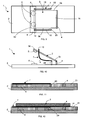
figures 2 et 3 représentent schématiquement, respectivement, une vue de dessus et une vue de face d'une première variante de réalisation d'un microsystème d'actionnement, avec une butée de fin de course d'ouverture d'un bras pivotant, selon l'invention. - Les
figures 4 à 8 sont des vues de face représentant schématiquement différentes étapes successives d'un procédé de fabrication d'un microsystème d'actionnement selon lesfigures 2 et 3 . - Les
figures 9 et 10 représentent schématiquement, respectivement, une vue de dessus et une vue de face d'une deuxième variante de réalisation d'un microsystème d'actionnement, avec une butée de fin de course d'ouverture d'un bras pivotant, selon l'invention. - Les
figures 11 à 13 sont des vues de face représentant schématiquement différentes étapes successives d'un procédé de fabrication d'un microsystème d'actionnement selon lesfigures 9 et 10 . - Dans le premier mode particulier de réalisation de l'invention représenté sur les
figures 2 à 8 , le microsystème d'actionnement 1 selon l'invention comporte le bras pivotant 3, par exemple en forme de plaque ayant deux bords longitudinaux 3a et 3b, montée en rotation autour de la charnière 4 au niveau d'une extrémité d'articulation 3c. Le bras pivotant 3 comporte, par exemple, deux plots de contact mobiles 5, placés au niveau d'une extrémité libre 3d du bras pivotant 3, opposée à l'extrémité d'articulation 3c, solidaires de la surface inférieure du bras pivotant 3 et destinés à coopérer avec, par exemple, deux plots de contact fixes 6, réalisés sur la surface supérieure du substrat 2. - Le microsystème 1 comporte, par exemple, deux butées de fin de course 7a, 7b d'ouverture du bras pivotant 3 (
figure 2 ), formées sur le substrat, disposées de part et d'autre du bras pivotant 3 et sur lesquelles viennent en butée, respectivement, les bords longitudinaux 3a, 3b du bras pivotant 3, afin de bloquer la rotation du bras pivotant 3. - Sur les
figures 2 et 3 , la description qui va suivre concerne une butée de fin de course 7 et s'applique pour les deux butées de fin de course 7a ,7b. La butée de fin de course 7 comporte un pied 8 et une tête 9, définissant une butée sensiblement en forme de champignon, faisant saillie au moins partiellement au-dessus du bord longitudinal 3a, 3b correspondant du bras pivotant 3. Le pied 8 de la butée 7 est disposé entre la charnière 4 et le plot de contact fixe 6, réalisés sur le substrat 2 (figure 2 ), et le pied 8 est constitué en trois parties. - Sur la
figure 3 , la première partie du pied 8 est un plot de support 10, formé sur le substrat 2 et, de préférence, dans un même matériau que la charnière 4, notamment tout matériau qui ne se dégrade pas pendant la libération par gravure du bras pivotant 3 lors du procédé de fabrication comme décrit ci-après. La deuxième partie du pied 8 est un piédestal 11, prolongeant le plot de support 10 et formé, de préférence, dans un même matériau que le bras pivotant 3. La troisième partie du pied 8 est une portion de support 12 de la tête 9, formée, de préférence, dans un même matériau que la tête 9. - La tête 9 de la butée de fin de course 7 est, par exemple, bombée, pour définir sensiblement la forme caractéristique d'un chapeau de champignon, et fait saillie au-dessus du bord longitudinal 3a, 3b associé du bras pivotant 3, afin de bloquer la rotation du bras pivotant 3 et donc servir de butée de fin de course, pour l'ouverture du bras pivotant 3. La forme caractéristique en champignon de la tête 9 de la butée de fin de course 7 est obtenue avantageusement par dépôt électrolytique d'un matériau compatible avec ce type de procédé, notamment tout matériau métallique, apte à supporter les étapes de gravure permettant la libération du microsystème comme décrit ci-après.
- À titre d'exemple, la tête 9 et la portion de support 12 de la tête 9 sont en fer, en nickel, en or, en chrome ou en tout alliage comportant au moins deux de ces matériaux. La portion de support 12 de la tête 9 a une épaisseur de l'ordre de 1µm à 5µm. Le bras pivotant 3 est composé d'une couche en matériau ferromagnétique, par exemple un alliage de nickel et de fer, et a une épaisseur de l'ordre de 5µm à 10µm. Le plot de support 10 et la charnière 4 sont en chrome, en nickel, en or ou en alliage de chrome et nickel, en alliage de nickel et or ou, avantageusement, en alliage de chrome, nickel et or.
- Par ailleurs, la tête 9 de la butée 7 est, par exemple, de forme bombée, circulaire et présente un diamètre supérieur à la largeur de la portion de support 12 d'une distance d de l'ordre de 2µm. De telles dimensions permettent donc de déterminer un angle d'ouverture prédéterminé pour le bras pivotant 3, pour sa rotation autour de la charnière 4, jusqu'à venir en butée contre la tête 9 de la butée de fin de course 7 (
figure 3 ). - Un procédé de fabrication selon l'invention du microsystème 1, comme représenté sur les
figures 2 et 3 , va être décrit plus en détail au regard desfigures 4 à 8 . Sur lafigure 4 , le procédé comporte, dans une première étape, la formation des plots de contact fixe 6 sur la surface supérieure du substrat 2, puis, dans une deuxième étape, la formation de préférence simultanée, de la charnière 4 et des plots de support 10 des pieds 8 des butées de fin de course 7 (figure 3 ). Les plots de support 10 sont formés entre la charnière 4 et les plots de contact fixes 6, par structuration d'une première couche d'un même matériau, par exemple en chrome, en nickel, en or ou en alliage de chrome et nickel, déposée sur le substrat 2 et les plots de contact fixes 6 préalablement formés. - Sur la
figure 4 , une couche sacrificielle 13, par exemple en oxyde de silicium (SiO2), formée, par exemple, par un dépôt chimique en phase vapeur assisté par plasma (communément appelé « Plasma Enhanced Chemical Vapor Déposition » ou PECVD en anglais) est ensuite formée, dans une troisième étape, autour de la charnière 4, des plots de support 10 et des plots de contact fixes 6. Dans une quatrième étape, une couche conductrice, par exemple en or, en nickel, en chrome, en platine ou en ruthénium, d'épaisseur de l'ordre de 0,1µm à 1µm, est ensuite déposée sur la couche sacrificielle 13, de manière à former au moins un plot de contact mobile 5 sur la surface inférieure du bras pivotant 3, destiné à venir en contact sur les plots de contact fixes 6 associés. - Sur la
figure 4 , dans une cinquième étape, le procédé comporte ensuite la formation du bras pivotant 3 dans une deuxième couche, par exemple en alliage de nickel et de fer, à partir d'une couche conductrice 14, par exemple en nickel, en or ou en alliage de nickel et de fer, d'épaisseur de l'ordre de 0,1µm, déposée sur la couche sacrificielle 13 et structurée de manière à permettre un dépôt notamment par croissance électrolytique. Plus particulièrement, la cinquième étape consiste à déposer un masque 15 de résine photosensible, par exemple avec une épaisseur de l'ordre de 5µm à 10µm, sur la couche conductrice 14, le masque 15 étant partiellement ouvert selon la forme prédéterminée du bras pivotant 3 et du piédestal 11, prolongeant le plot de support 10, à réaliser. Puis, le bras pivotant 3 et le piédestal 11 du pied 8 de la butée de fin de course 7 sont formés, avantageusement, simultanément, par exemple, par dépôt électrolytique d'une couche en alliage de nickel et de fer. - Sur les
figures 5 et 6 , la couche conductrice 14 est avantageusement gravée selon la forme désirée, par l'intermédiaire d'un masque (figure 5 ), afin de conserver un contact électrique pour le piédestal 11. Puis, un masque 16, par exemple en résine photosensible, est déposé sur le bras pivotant 3 et le piédestal 11. Le masque 16 est ensuite gravé, de manière à former une ouverture 17 au niveau du piédestal 11 (figure 6 ). - Une troisième couche, par exemple en alliage de nickel et de fer, est alors déposée, par exemple, par dépôt électrolytique d'abord jusqu'à la limite supérieure du masque 16, pour former la portion de support 12 de la tête 9, constituant la troisième partie du pied 8 de la butée 7, et ensuite par débordement du matériau au-dessus du bras pivotant 3, pour former la tête 9 de la butée de fin de course 7.
- Sur les
figures 7 et 8 , le masque 16 est ensuite éliminé, par exemple par gravure (figure 7 ), et le reliquat de la couche conductrice 14 est alors éliminé également par gravure. Enfin, dans une sixième étape, la couche sacrificielle 13 est éliminée, par exemple par gravure à l'acide fluorhydrique, afin de libérer le bras pivotant 3. Un microsystème 1 comme représenté schématiquement sur lesfigures 2, 3 et8 est ainsi obtenu, avec la fabrication des butées de fin de course 7 réalisée de manière simple par des étapes de fabrication classiques en microélectronique, intégrées dans les étapes de fabrication du microsystème 1 lui-même. Il en résulte un gain en termes de temps et surtout en termes de coûts de fabrication. - Dans la variante de réalisation de l'invention représentée sur les
figures 9 à 13 , le microsystème d'actionnement 1 selon l'invention se distingue du microsystème 1 représenté sur lesfigures 2 à 8 par la forme de la butée de fin de course 7 d'ouverture du bras pivotant 3. - Sur les
figures 9 et 10 , la butée de fin de course 7 est en forme de U, définissant sensiblement un portique comportant deux branches latérales 18 sous contrainte, reliées par une branche transversale 19, qui peut être dans un même matériau ou dans un matériau différent des branches latérales 18. Plus particulièrement, la branche transversale 19 est en tout matériau isolant, semi-conducteur ou conducteur non soluble dans l'acide fluorhydrique, par exemple du nitrure de silicium, du silicium, du nickel, du chrome, de l'or ou tout alliage à base de nickel, de chrome et d'or. - Le terme « sous contrainte » signifie qu'au moins les branches latérales 18 de la butée de fin de course 7 sont composées de couches de matériaux différents, c'est-à-dire ayant des coefficients de dilatation thermique différents ou des états de contraintes différents. Il en résulte alors leur déformation après relaxation des contraintes, leur permettant notamment de prendre une position sensiblement relevée au repos (
figures 10 et13 ), comme décrit notamment dans l'article « Effect of width on the stress-induced bending of micromachined bilayer cantilevers » de Max Ti-Kuang Hou et al. (J. Micromech. Microeng. 13 (2003) pp.141-148) et dans l'article « Curled micro-cantilevers using benzocyclobutene polymer and Mo for wafer level probing » de Si-Hyung Lee et al. (Sensors et Actuators A 121 (2005) pp.472-479). - Sur les
figures 9 et 10 , les branches latérales 18 sont disposées de part et d'autre du bras pivotant 3, parallèlement aux bords longitudinaux 3a, 3b, et ont une première extrémité reliée au substrat 2 par un plot de support 20 correspondant et une seconde extrémité reliée à la branche transversale 19. Les plots de support 20 sont disposés latéralement par rapport au bras pivotant 3 (figure 9 ), entre la charnière 4 et les plots de contact fixes 6, et les branches latérales 18 de la butée de fin de course 7 sont orientées de sorte que la branche transversale 19 est située à l'opposé de la charnière 4 (figure 10 ). - Les branches latérales 18 sont coudées vers le haut (
figure 10 ) et la branche transversale 19 est disposée au-dessus et à distance du bras pivotant 3, entre l'extrémité 3c du bras pivotant 3, articulée sur la charnière 4, et l'extrémité libre 3d du bras pivotant 3, associée au plot de contact mobile 5. - La forme particulière relevée vers le haut des branches latérales 18, permettant à la branche transversale 19 d'être placée au-dessus du bras pivotant 3 et de servir de butée, pour bloquer la rotation du bras pivotant 3, est notamment due aux matériaux sous contrainte utilisés pour fabriquer la butée de fin de course 7, comme décrit ci-après.
- Dans le mode particulier de réalisation représenté sur les
figures 9 à 13 , au moins les branches latérales 18 de la butée de fin de course 7 sont donc composées d'un empilement de couches sous contrainte, de préférence un empilement d'une couche en métal et d'une couche en polymère ou un empilement d'une couche en métal et d'une couche en nitrure de silicium. - À titre d'exemple, l'empilement composant la butée de fin de course 7 est composé d'une couche de nickel, par exemple avec une épaisseur de l'ordre de 0,1µm, et d'une couche de nitrure de silicium, avec une épaisseur de l'ordre de 0,2µm. Par ailleurs, comme précédemment, le bras pivotant 3 est composé, de préférence, d'une couche en matériau ferromagnétique, par exemple un alliage de nickel et de fer, et a une épaisseur de l'ordre de 5µm à 10µm.
- À titre d'exemple, la butée de fin de course 7 peut être composée d'un empilement d'une couche de molybdène et d'une couche de benzocyclobutène (plus communément appelé BCB), notamment dans le cas où la butée de fin de course 7 est composée d'un empilement de couches sous contrainte différentielle, c'est-à-dire des couches ayant des coefficients de dilatation thermique différents ou des états de contraintes différents. En effet, les mécanismes de déformation par contrainte étant très liés aux modes d'élaboration des couches et à leurs propriétés mécaniques, les dimensionnements de dispositifs obtenus par simulations numériques s'avèrent peu pertinents. L'approche par itérations successives sur les épaisseurs et les comparaisons de jeux de formes à variation progressive permettent ainsi de définir une forme propre à assurer un blocage à une hauteur définie.
- Un procédé de fabrication du microsystème 1, selon l'invention, comme représenté sur les
figures 9 et 10 , va être décrit plus en détail au regard desfigures 11 à 13 . Le procédé comporte, comme pour la variante de réalisation précédente, les six mêmes étapes, mais la fabrication de la butée de fin de course 7 s'effectue entre la troisième étape et la quatrième étape, à savoir après l'étape de formation d'une couche sacrificielle 21 (figure 11 ) et avant l'étape de formation d'une couche conductrice pour la réalisation de plots de contact mobiles 5 associés au bras pivotant 3 (figure 12 ). - Sur la
figure 11 , le procédé comporte donc d'abord la formation des plots de support 20 des branches latérales 18 de la butée de fin de course 7 et, de préférence simultanément, la formation de la charnière 4, sur laquelle est montée en rotation le bras pivotant 3. Puis, une couche sacrificielle 21, par exemple en oxyde de silicium, avec une épaisseur de l'ordre de 1µm à 5µm, est déposée, par exemple par PECVD. Un empilement de couches sous contrainte est ensuite déposé sur la couche sacrificielle 21 et gravé selon la forme souhaitée de la butée de fin de course 7, à savoir en forme de portique en U (figure 9 ). - Sur la
figure 12 , la couche conductrice 14 est ensuite déposée sur la couche sacrificielle 21, correspondant à la quatrième étape, et le bras pivotant 3 est ensuite formé, comme précédemment, sur la couche conductrice 14, par exemple par croissance électrolytique, entre les branches latérales 18 de la butée de fin de course 7. - Enfin, comme représenté sur la
figure 13 , après l'élimination de la couche sacrificielle 21, les contraintes dans l'empilement de couches composant la butée de fin de course 7 provoquent ainsi le relèvement de la butée de fin de course 7, avec la branche transversale 19 qui vient ainsi limiter mécaniquement la course verticale du bras pivotant 3 et les branches latérales 18 qui se courbent vers le haut. La branche transversale 19 vient ainsi se placer au-dessus de l'extrémité libre 3d du bras pivotant 3, entre l'extrémité libre 3d et l'extrémité 3c articulée sur la charnière 4 du bras pivotant 3. - Quel que soit le mode de réalisation décrit ci-dessus, le microsystème 1 selon l'invention comporte ainsi une butée de fin de course 7 efficace, avec une rotation du bras pivotant 3 limitée en fonction de la hauteur et de la position de la partie supérieure de la butée 7, laquelle est disposée au-dessus et à distance du bras pivotant 3, entre l'extrémité d'articulation 3c et l'extrémité libre 3d du bras pivotant 3. La hauteur et la position de la butée de fin de course 7 par rapport au bras pivotant 3 déterminent ainsi l'angle d'ouverture, à savoir l'amplitude de rotation possible, du bras pivotant 3 et le blocage du bras pivotant 3 est obtenu par l'appui sur une portion de la butée 7 venant se positionner en surplomb du bras pivotant 3.
- Par ailleurs, l'avantage principal d'un tel microsystème 1, quel que soit le mode de réalisation représenté sur les
figures 2 et 3 (première variante) et 9 et 10 (deuxième variante), réside dans le fait que la fabrication de la butée de fin de course 7 est intégrée dans les étapes de fabrication du microsystème 1 lui-même, quelle que soit la forme de la butée de fin de course 7. Le procédé selon l'invention propose ainsi de fabriquer la butée de fin de course 7 sur le substrat 2 supportant le bras pivotant 3, au cours du procédé de fabrication de celui-ci et à l'aide d'étapes de microélectronique. Ainsi, à l'aide des couches utilisées pour la fabrication du microsystème 1 et de l'addition de nouvelles étapes de fabrication, il est possible de réaliser une structure de blocage intégrée au support du microsystème, tout en maîtrisant l'angle d'ouverture possible du bras pivotant et en conservant le bénéfice de l'intégration. - Par ailleurs, un tel microsystème 1 selon l'invention (
figures 2 à 13 ) présente également les avantages suivants. Le microsystème 1 ne nécessite pas de positionnement mécanique spécifique du bras pivotant 3 par rapport à la butée de fin de course 7. Le microsystème 1 est réalisé selon des techniques classiques en microélectronique, il en résulte une précision au micron des dimensions du microsystème 1 obtenu et une grande reproductibilité du procédé de fabrication. - Un tel procédé de fabrication selon l'invention (
figures 2 à 13 ) est donc facile à mettre en oeuvre et ne nécessite aucun coût supplémentaire, notamment grâce à l'utilisation de techniques classiques en microélectronique et à l'intégration de la fabrication de la butée de fin de course pendant la fabrication du microsystème. Par ailleurs, il est possible de changer facilement l'amplitude de rotation du bras pivotant 3 sur le substrat 2, uniquement en changeant la forme et les dimensions des masques utilisés pour la fabrication du bras pivotant 3 et de la butée de fin de course 7, plus particulièrement pour la réalisation de la portion de support de tête 12 du pied 8, dans la première variante de réalisation (figures 2 à 8 ), et pour la réalisation de l'empilement sous contrainte des couches composant la butée 7, dans la deuxième variante de réalisation (figures 9 à 13 ). - Un tel microsystème d'actionnement et un tel procédé de fabrication selon l'invention s'appliquent notamment chaque fois qu'il convient de limiter la course d'un élément mobile sur un dispositif par des moyens intégrés à ce dispositif, plus particulièrement chaque fois que la partie mobile d'un interrupteur peut se déformer et ainsi nuire aux propriétés mécaniques de celui-ci. Ce type d'interrupteur peut se retrouver notamment dans des produits de type domestique, automobile, télécommunication, etc., où la miniaturisation apporte des avantages de fiabilité et de réduction de coûts.
- L'invention n'est pas limitée aux différents modes de réalisation décrits ci-dessus. D'une façon générale, le microsystème 1 peut comporter tout type de butée de fin de course 7, solidaire du substrat, quelles que soient sa forme et ses dimensions, tant que la butée de fin de course 7 comporte une portion supérieure disposée au-dessus et à distance du bras pivotant 3, destinée à bloquer la rotation du bras pivotant 3, et une partie inférieure reliée au substrat et disposée latéralement par rapport au bras pivotant 3. Le microsystème 1 peut être réalisé par tout type de procédé de fabrication, de préférence tant que la fabrication de la butée de fin de course 7 est intégrée à la fabrication du microsystème 1 lui-même.
Claims (18)
- Microsystème d'actionnement (1) réalisé sur un substrat plan (2) et comportant au moins :- un bras pivotant (3), monté en rotation autour d'une charnière (4) formée sur le substrat (2),- un premier plot de contact fixe (6), disposé sur une surface supérieure du substrat (2) et coopérant avec au moins un plot de contact mobile (5), solidaire du bras pivotant (3),- et une butée de fin de course (7) d'ouverture du bras pivotant (3),microsystème caractérisé en ce que la butée de fin de course (7), formée sur le substrat, comporte :- une partie supérieure disposée au-dessus et à distance du bras pivotant (3), entre une extrémité d'articulation (3c) du bras pivotant (3) sur la charnière (4) et une extrémité libre (3d) du bras pivotant (3), comportant le plot de contact mobile (5),- une partie inférieure, reliée au substrat (2) et disposée latéralement par rapport au bras pivotant (3), entre la charnière (4) et le plot de contact fixe (6).
- Microsystème selon la revendication 1, caractérisé en ce que le bras pivotant (3) comporte une couche en matériau ferromagnétique.
- Microsystème selon la revendication 2, caractérisé en ce que le bras pivotant (3) comporte une couche en alliage de nickel et de fer.
- Microsystème selon l'une quelconque des revendications 1 à 3, caractérisé en ce que le bras pivotant (3) a une épaisseur de l'ordre de 5µm à 10µm.
- Microsystème selon l'une quelconque des revendications 1 à 4, caractérisé en ce que :- la partie supérieure de la butée de fin de course (7) est constituée par une tête (9), faisant saillie au moins partiellement au-dessus d'un bord longitudinal (3a, 3b) du bras pivotant (3),- la partie inférieure de la butée de fin de course (7) est constituée par un pied (8), comprenant un plot de support (10), formé sur le substrat (2), un piédestal (11) prolongeant le plot de support (10) et une portion de support (12) de la tête (9).
- Microsystème selon la revendication 5, caractérisé en ce que le plot de support (10) est réalisé en un même matériau que la charnière (4), le piédestal (11) est réalisé en un même matériau que le bras pivotant (3) et la portion de support (12) de la tête (9) est réalisée en un même matériau que la tête (9).
- Microsystème selon l'une des revendications 5 et 6, caractérisé en ce que la tête (9) et la portion de support (12) de la tête (9) de la butée de fin de course (7) sont réalisées en un matériau obtenu par dépôt électrolytique.
- Microsystème selon l'une quelconque des revendications 5 à 7, caractérisé en ce que la portion de support (12) de la tête (9) de la butée de fin de course (7) a une épaisseur de l'ordre de 1µm à 5µm.
- Microsystème selon l'une quelconque des revendications 5 à 8, caractérisé en ce qu'il comporte deux butées de fin de course (7a, 7b), disposées de part et d'autre de bords longitudinaux (3a, 3b) du bras pivotant (3).
- Microsystème selon l'une quelconque des revendications 1 à 4, caractérisé en ce que la butée de fin de course (7) est en forme de U, comportant deux branches latérales (18) sous contrainte, constituant la partie inférieure de la butée de fin de course (7), disposées de part et d'autre du bras pivotant (3), coudées vers le haut et reliées par une branche transversale (19), constituant la partie supérieure de la butée de fin de course (7).
- Microsystème selon la revendication 10, caractérisé en ce que les branches latérales (18) de la butée de fin de course (7) sont composées d'un empilement de couches sous contrainte.
- Microsystème selon la revendication 11, caractérisé en ce que les branches latérales (18) de la butée de fin de course (7) sont composées d'un empilement d'une couche en métal et d'une couche en polymère.
- Microsystème selon la revendication 11, caractérisé en ce que les branches latérales (18) de la butée de fin de course (7) sont composées d'un empilement d'une couche en métal et d'une couche en nitrure de silicium.
- Microsystème selon la revendication 13, caractérisé en ce que les branches latérales (18) de la butée de fin de course (7) sont composées d'une couche de nickel, d'épaisseur de l'ordre de 0,1µm, et d'une couche de nitrure de silicium, d'épaisseur de l'ordre de 0,2µm.
- Microsystème selon la revendication 11, caractérisé en ce que les branches latérales (18) de la butée de fin de course (7) sont composées d'un empilement d'une couche de molybdène et d'une couche de benzocyclobutène.
- Microsystème selon l'une quelconque des revendications 10 à 15, caractérisé en ce que la branche transversale (19) est composée d'un empilement de couches sous contrainte.
- Procédé de fabrication d'un microsystème (1), selon l'une quelconque des revendications 5 à 9, comportant successivement :- une première étape, de formation d'au moins un plot de contact fixe (6) sur le substrat (2),- une deuxième étape, de formation d'une charnière (4) et, entre la charnière (4) et le plot de contact fixe (6), d'au moins un plot de support (10) de la butée (7) dans une première couche déposée sur le substrat (2) et le plot de contact fixe (6),- une troisième étape, de formation d'une couche sacrificielle (13) entre la charnière (4), le plot de support (10) et le plot de contact fixe (6),- une quatrième étape, de formation d'au moins un plot de contact mobile (5) dans une couche conductrice,- une cinquième étape, de formation d'un bras pivotant (3) par croissance électrolytique d'une deuxième couche à partir d'une couche conductrice (14), déposée sur le plot de contact mobile (5) et la couche sacrificielle (13),- une sixième étape, d'élimination de la couche sacrificielle (13),procédé caractérisé en ce qu'il comporte, entre la cinquième étape et la sixième étape, les étapes successives suivantes de :- formation dans la deuxième couche, en même temps que le bras pivotant (3), d'un piédestal (11) prolongeant le plot de support (10),- formation d'une ouverture (17) au niveau du piédestal (11), par dépôt et gravure d'un masque (16),- formation d'une portion de support (12) de la tête (9) et d'une tête (9) de la butée de fin de course (7) du bras pivotant (3), par dépôt et structuration d'une troisième couche,- élimination du masque (16).
- Procédé de fabrication d'un microsystème (1), selon l'une quelconque des revendications 10 à 16, comportant successivement :- une première étape, de formation d'au moins un plot de contact fixe (6) sur le substrat (2),- une deuxième étape, de formation d'une charnière (4) et, entre la charnière (4) et le plot de contact fixe (6), d'au moins un plot de support (20) de la butée (7) dans une première couche déposée sur le substrat (2) et le plot de contact fixe (6),- une troisième étape, de formation d'une couche sacrificielle (21) entre la charnière (4), le plot de support (20) et le plot de contact fixe (6),- une quatrième étape, de formation d'au moins un plot de contact mobile (5) dans une couche conductrice,- une cinquième étape, de formation d'un bras pivotant (3) par croissance électrolytique d'une deuxième couche à partir d'une couche conductrice (14), déposée sur le plot de contact mobile (5) et la couche sacrificielle (13),- une sixième étape, d'élimination de la couche sacrificielle (13),procédé caractérisé en ce que qu'il comporte, entre la troisième étape et la quatrième étape, la formation, par dépôt et structuration d'un empilement de couches sous contrainte, d'une butée de fin de course (7) en forme de U, comportant deux branches latérales (18), reliées par une branche transversale (19) et ayant chacune une extrémité solidaire d'un plot de support (20), l'élimination de la couche sacrificielle (21), lors de la sixième étape, provoquant le relèvement de la branche transversale (19) au-dessus de l'extrémité libre (3d) du bras pivotant (3).
Applications Claiming Priority (1)
| Application Number | Priority Date | Filing Date | Title |
|---|---|---|---|
| FR0700801A FR2912128B1 (fr) | 2007-02-05 | 2007-02-05 | Microsysteme d'actionnement et procede de fabrication associe |
Publications (2)
| Publication Number | Publication Date |
|---|---|
| EP1953116A2 true EP1953116A2 (fr) | 2008-08-06 |
| EP1953116A3 EP1953116A3 (fr) | 2008-08-27 |
Family
ID=38457905
Family Applications (1)
| Application Number | Title | Priority Date | Filing Date |
|---|---|---|---|
| EP20080354005 Withdrawn EP1953116A3 (fr) | 2007-02-05 | 2008-01-22 | Microsystème d'actionnement et procédé de fabrication associé |
Country Status (4)
| Country | Link |
|---|---|
| US (1) | US7834723B2 (fr) |
| EP (1) | EP1953116A3 (fr) |
| JP (1) | JP2008235254A (fr) |
| FR (1) | FR2912128B1 (fr) |
Cited By (1)
| Publication number | Priority date | Publication date | Assignee | Title |
|---|---|---|---|---|
| EP2204831A2 (fr) * | 2009-01-05 | 2010-07-07 | STMicroelectronics Asia Pacific Pte Ltd. | Système micro-électromécanique |
Families Citing this family (1)
| Publication number | Priority date | Publication date | Assignee | Title |
|---|---|---|---|---|
| FR2997247B1 (fr) | 2012-10-22 | 2016-12-09 | Commissariat Energie Atomique | Generateur d'electricite et recuperateur d'energie |
Citations (4)
| Publication number | Priority date | Publication date | Assignee | Title |
|---|---|---|---|---|
| US2709791A (en) | 1950-10-20 | 1955-05-31 | Jr Robert L Anderson | Saturable reactor |
| US20030173957A1 (en) | 2001-08-29 | 2003-09-18 | Microlab, Inc. | Micro magnetic proximity sensor |
| US6750745B1 (en) | 2001-08-29 | 2004-06-15 | Magfusion Inc. | Micro magnetic switching apparatus and method |
| US20050083156A1 (en) | 2003-10-15 | 2005-04-21 | Magfusion, Inc | Micro magnetic non-latching switches and methods of making same |
Family Cites Families (10)
| Publication number | Priority date | Publication date | Assignee | Title |
|---|---|---|---|---|
| US6418081B1 (en) * | 1998-02-10 | 2002-07-09 | The Research Foundation Of State University Of New York | System for detection of buried objects |
| US5990427A (en) * | 1998-10-23 | 1999-11-23 | Trw Inc. | Movable acceleration switch responsive to acceleration parallel to plane of substrate upon which the switch is fabricated and methods |
| DE10004393C1 (de) * | 2000-02-02 | 2002-02-14 | Infineon Technologies Ag | Mikrorelais |
| US6570750B1 (en) * | 2000-04-19 | 2003-05-27 | The United States Of America As Represented By The Secretary Of The Air Force | Shunted multiple throw MEMS RF switch |
| US6373007B1 (en) * | 2000-04-19 | 2002-04-16 | The United States Of America As Represented By The Secretary Of The Air Force | Series and shunt mems RF switch |
| US20030179058A1 (en) * | 2002-01-18 | 2003-09-25 | Microlab, Inc. | System and method for routing input signals using single pole single throw and single pole double throw latching micro-magnetic switches |
| US20030137374A1 (en) * | 2002-01-18 | 2003-07-24 | Meichun Ruan | Micro-Magnetic Latching switches with a three-dimensional solenoid coil |
| JP2003242873A (ja) * | 2002-02-19 | 2003-08-29 | Fujitsu Component Ltd | マイクロリレー |
| JP4364565B2 (ja) * | 2003-07-02 | 2009-11-18 | シャープ株式会社 | 静電アクチュエーター,マイクロスイッチ,マイクロ光スイッチ,電子機器および静電アクチュエーターの製造方法 |
| FR2880730A1 (fr) * | 2005-01-10 | 2006-07-14 | Schneider Electric Ind Sas | Microsysteme utilisant un microactionneur magnetique a aimant permanent. |
-
2007
- 2007-02-05 FR FR0700801A patent/FR2912128B1/fr not_active Expired - Fee Related
-
2008
- 2008-01-22 EP EP20080354005 patent/EP1953116A3/fr not_active Withdrawn
- 2008-01-28 US US12/010,628 patent/US7834723B2/en not_active Expired - Fee Related
- 2008-02-05 JP JP2008025039A patent/JP2008235254A/ja active Pending
Patent Citations (4)
| Publication number | Priority date | Publication date | Assignee | Title |
|---|---|---|---|---|
| US2709791A (en) | 1950-10-20 | 1955-05-31 | Jr Robert L Anderson | Saturable reactor |
| US20030173957A1 (en) | 2001-08-29 | 2003-09-18 | Microlab, Inc. | Micro magnetic proximity sensor |
| US6750745B1 (en) | 2001-08-29 | 2004-06-15 | Magfusion Inc. | Micro magnetic switching apparatus and method |
| US20050083156A1 (en) | 2003-10-15 | 2005-04-21 | Magfusion, Inc | Micro magnetic non-latching switches and methods of making same |
Non-Patent Citations (2)
| Title |
|---|
| HOU ET AL., J. MICROMECH. MICROENG., vol. 13, 2003, pages 141 - 148 |
| SI-HYUNG LEE ET AL., SENSORS ET ACTUATORS, vol. 121, 2005, pages 472 - 479 |
Cited By (1)
| Publication number | Priority date | Publication date | Assignee | Title |
|---|---|---|---|---|
| EP2204831A2 (fr) * | 2009-01-05 | 2010-07-07 | STMicroelectronics Asia Pacific Pte Ltd. | Système micro-électromécanique |
Also Published As
| Publication number | Publication date |
|---|---|
| JP2008235254A (ja) | 2008-10-02 |
| US20080186117A1 (en) | 2008-08-07 |
| EP1953116A3 (fr) | 2008-08-27 |
| US7834723B2 (en) | 2010-11-16 |
| FR2912128B1 (fr) | 2009-05-22 |
| FR2912128A1 (fr) | 2008-08-08 |
Similar Documents
| Publication | Publication Date | Title |
|---|---|---|
| EP1040492B1 (fr) | Microsysteme a element deformable sous l'effet d'un actionneur thermique | |
| EP0766060B1 (fr) | Procédé de fabrication de pièces de micromécanique ayant une partie en diamant constituée au moins d'une pointe. | |
| EP2019811B1 (fr) | Microcomposant muni d'une cavite delimitee par un capot a resistance mecanique amelioree | |
| EP2829508B1 (fr) | Structure d'encapsulation comprenant un capot renforce mécaniquement et à effet getter | |
| EP2298693B1 (fr) | Réalisation d'un composant électromecanique pour un micro- ou nano- système doté d'un barreau formant un axe de rotation du composant et recouvert de graphène | |
| EP0719951A1 (fr) | Micro-électro aimant à circuit magnétique et bobine intégrés | |
| EP1458095B1 (fr) | Procédé de réalisation d'un microrésonateur piézoélectrique accordable | |
| EP2138455B1 (fr) | Procédé de réalisation d'une structure MEMS comportant un élément mobile au moyen d'une couche sacrificielle hétérogène | |
| EP2670700B1 (fr) | Méthode de fabrication d'une pièce de micromécanique complexe et à faible rugosité | |
| FR3120622A1 (fr) | Commutateur MEMS à commande électrique et son procédé de réalisation | |
| FR2820833A1 (fr) | Micro-miroir optique a pivot, matrice de tels micro-miroirs et procede de realisation dudit micro-miroir | |
| FR2912128A1 (fr) | Microsysteme d'actionnement et procede de fabrication associe | |
| EP2226678B1 (fr) | Procédé de fabrication d'un moule pour la lithographie par nano-impression | |
| FR2904304A1 (fr) | Procede de fabrication d'une nanostructure sur un substrat pre-grave. | |
| WO2009083565A2 (fr) | Dispositif micromecanique ou nanomecanique a couche d'interface anti-collage | |
| FR2862806A1 (fr) | Composant incluant un condensateur variable | |
| EP3828943A1 (fr) | Microsystème mécanique et procédé de fabrication associé | |
| WO2016102827A1 (fr) | Dispositif microelectromecanique ou nanoelectromecanique comportant une membrane profilee mobile en translation | |
| FR3143256A1 (fr) | Elément actif piézoélectrique pour système électromécanique | |
| EP2472542A1 (fr) | Procédé de fabrication d'un micro-contacteur actionnable par un champ magnétique | |
| EP1846320A1 (fr) | Dispositif micromecanique comportant une poutre mobile | |
| FR3125810A1 (fr) | Procede de realisation de cavite au sein d’un empilement de materiaux | |
| FR2871790A1 (fr) | Microressort de grande amplitude | |
| FR3031098A1 (fr) | Dispositif microelectromecanique ou nanoelectromecanique comportant une membrane mobile en translation et une electrode d'actionnement isolee de la membrane par une couche dielectrique | |
| FR3076074A1 (fr) | Procede de fabrication d'un dispositif traversant |
Legal Events
| Date | Code | Title | Description |
|---|---|---|---|
| PUAI | Public reference made under article 153(3) epc to a published international application that has entered the european phase |
Free format text: ORIGINAL CODE: 0009012 |
|
| PUAL | Search report despatched |
Free format text: ORIGINAL CODE: 0009013 |
|
| AK | Designated contracting states |
Kind code of ref document: A2 Designated state(s): AT BE BG CH CY CZ DE DK EE ES FI FR GB GR HR HU IE IS IT LI LT LU LV MC MT NL NO PL PT RO SE SI SK TR |
|
| AX | Request for extension of the european patent |
Extension state: AL BA MK RS |
|
| AK | Designated contracting states |
Kind code of ref document: A3 Designated state(s): AT BE BG CH CY CZ DE DK EE ES FI FR GB GR HR HU IE IS IT LI LT LU LV MC MT NL NO PL PT RO SE SI SK TR |
|
| AX | Request for extension of the european patent |
Extension state: AL BA MK RS |
|
| 17P | Request for examination filed |
Effective date: 20090213 |
|
| AKX | Designation fees paid |
Designated state(s): AT BE BG CH CY CZ DE DK EE ES FI FR GB GR HR HU IE IS IT LI LT LU LV MC MT NL NO PL PT RO SE SI SK TR |
|
| RAP1 | Party data changed (applicant data changed or rights of an application transferred) |
Owner name: COMMISSARIAT A L'ENERGIE ATOMIQUE ET AUX ENERGIES |
|
| 17Q | First examination report despatched |
Effective date: 20150324 |
|
| STAA | Information on the status of an ep patent application or granted ep patent |
Free format text: STATUS: THE APPLICATION IS DEEMED TO BE WITHDRAWN |
|
| 18D | Application deemed to be withdrawn |
Effective date: 20150804 |