EP1952168B1 - Integrated circuit arrangement and design method - Google Patents
Integrated circuit arrangement and design method Download PDFInfo
- Publication number
- EP1952168B1 EP1952168B1 EP06809673A EP06809673A EP1952168B1 EP 1952168 B1 EP1952168 B1 EP 1952168B1 EP 06809673 A EP06809673 A EP 06809673A EP 06809673 A EP06809673 A EP 06809673A EP 1952168 B1 EP1952168 B1 EP 1952168B1
- Authority
- EP
- European Patent Office
- Prior art keywords
- compaction
- test
- integrated circuit
- network
- logic
- Prior art date
- Legal status (The legal status is an assumption and is not a legal conclusion. Google has not performed a legal analysis and makes no representation as to the accuracy of the status listed.)
- Not-in-force
Links
- 238000000034 method Methods 0.000 title claims description 14
- 238000013461 design Methods 0.000 title claims description 10
- 238000012360 testing method Methods 0.000 claims abstract description 106
- 238000005056 compaction Methods 0.000 claims abstract description 95
- 230000007480 spreading Effects 0.000 claims abstract description 30
- 239000011159 matrix material Substances 0.000 claims description 38
- 239000013598 vector Substances 0.000 claims description 30
- 230000008878 coupling Effects 0.000 claims description 5
- 238000010168 coupling process Methods 0.000 claims description 5
- 238000005859 coupling reaction Methods 0.000 claims description 5
- 239000000243 solution Substances 0.000 description 9
- 230000004044 response Effects 0.000 description 7
- 230000008901 benefit Effects 0.000 description 5
- 238000001514 detection method Methods 0.000 description 3
- 238000013459 approach Methods 0.000 description 2
- 230000006835 compression Effects 0.000 description 2
- 238000007906 compression Methods 0.000 description 2
- 230000000694 effects Effects 0.000 description 2
- 238000012545 processing Methods 0.000 description 2
- 238000004891 communication Methods 0.000 description 1
- 230000001419 dependent effect Effects 0.000 description 1
- 238000002955 isolation Methods 0.000 description 1
- 238000004519 manufacturing process Methods 0.000 description 1
- 230000007246 mechanism Effects 0.000 description 1
- 239000012085 test solution Substances 0.000 description 1
- 230000001960 triggered effect Effects 0.000 description 1
Images


Classifications
-
- G—PHYSICS
- G01—MEASURING; TESTING
- G01R—MEASURING ELECTRIC VARIABLES; MEASURING MAGNETIC VARIABLES
- G01R31/00—Arrangements for testing electric properties; Arrangements for locating electric faults; Arrangements for electrical testing characterised by what is being tested not provided for elsewhere
- G01R31/28—Testing of electronic circuits, e.g. by signal tracer
- G01R31/317—Testing of digital circuits
- G01R31/31703—Comparison aspects, e.g. signature analysis, comparators
-
- G—PHYSICS
- G01—MEASURING; TESTING
- G01R—MEASURING ELECTRIC VARIABLES; MEASURING MAGNETIC VARIABLES
- G01R31/00—Arrangements for testing electric properties; Arrangements for locating electric faults; Arrangements for electrical testing characterised by what is being tested not provided for elsewhere
- G01R31/28—Testing of electronic circuits, e.g. by signal tracer
- G01R31/317—Testing of digital circuits
- G01R31/3181—Functional testing
- G01R31/319—Tester hardware, i.e. output processing circuits
- G01R31/3193—Tester hardware, i.e. output processing circuits with comparison between actual response and known fault free response
- G01R31/31932—Comparators
Definitions
- the present invention relates to an integrated circuit (IC) arrangement having space compaction logic for compacting a test result from the digital outputs of the IC in the arrangement.
- IC integrated circuit
- the present invention further related to a method for designing such space compaction logic.
- IC testing is rapidly becoming a dominating factor in the manufacturing costs of ICs.
- One of the main reasons for this is that for complex ICs testing is time-consuming. This is mainly because large amounts of test input and output data have to be communicated with the IC under test. Consequently, measures to reduce the size of the data involved in this communication have attracted considerable attention.
- test solutions have been disclosed in which digital test input data has been compacted, with the IC having an on-board extractor for restoring the test input data to its original size.
- the digital test outputs of the IC under test have been compacted by an on-board compactor, and the IC test results are provided to the outside world in this compacted form.
- An example of this approach can be found in: " Parity-based output compaction for core-based SOCs" by Sinanoglu et al., Proc. Of the Eight IEEE European Test Workshop, pages 15-20, IEEE ETW 2003 .
- each compacted test response to a test input e.g. a test vector provided to the IC under test is analyzed to determine whether the provided test vector triggered the detection of a fault.
- a drawback of using compacted test results is that at least some test resolution may be lost, especially when using parity-tree based compactors, which are typically based on exclusive OR (XOR) logic gates.
- XOR exclusive OR
- the occurrence of a fault producing an even number of faulty bits on the outputs of the IC that are fed into the compactor, or the simultaneous occurrence of multiple faults may lead to the faulty bits cancelling each other out.
- determining the location of the fault may become more difficult because of fault aliasing, which occurs when multiple faults produce the same faulty bits on the outputs of the space compaction logic, which means that the compacted test response is only indicative of the occurrence of a number of faulty bits without the possibility of assigning them to a specific fault.
- the present invention seeks to provide an integrated circuit arrangement according to the opening paragraph with improved test resolution.
- the present invention further seeks to provide a method for designing space compaction logic for such an arrangement.
- an integrated circuit arrangement comprising an integrated circuit comprising plurality of digital outputs, each of the outputs being arranged to provide a test result in a test mode of the integrated circuit, and space compaction logic comprising a space compaction network having a plurality of compaction domains, each domain being arranged to compact a plurality of test results into a further test result, and a spreading network coupled between the plurality of digital outputs and the space compaction network, the spreading network being arranged to duplicate each test result from the digital outputs to a number of compaction domains.
- each compaction domain is coupled to a unique set of digital outputs, because this minimizes the chance of cancellation and/or aliasing effects occurring in all domains.
- the spreading network is configurably coupled to the digital outputs of the IC to facilitate bypassing the space compaction logic in functional (i.e. operational) mode of the IC.
- the space compaction network may be located on the IC, with its outputs being directly observable at at least some of the pins of the IC. This has the advantage that the test results are readily available, e.g. after every cycle of the test clock, which facilitates fast processing of the test results.
- each compaction domain has an output for producing its further test result
- the integrated circuit further comprising a shift register for serially shifting data towards a test data output of the integrated circuit, the respective outputs of the compaction domains being coupled to respective cells of the shift register.
- the space compaction logic may also be located outside the IC, e.g. as part of a test means including an automated test apparatus and a load board for coupling the integrated circuit to the test apparatus, with the space compaction logic located either on the load board or the test apparatus.
- a method for designing space compaction logic for testing an integrated circuit having a plurality of digital outputs comprising a space compaction network having a plurality of compaction domains having m outputs, each domain being arranged to compact a plurality of test results into a further test result, and a spreading network having n inputs for coupling between the plurality of digital outputs and the space compaction network, the spreading network being arranged to duplicate each test result from the digital outputs to f compaction domains, f, n and m being positive integers with n being larger than m, and m being larger than f, the method comprising generating a set of bit vectors, each vector comprising m bits, each bit indicating the presence of a conductive path from an input of the spreading network to an output of the space compaction network, the total number of conductive paths per vector being f and combining n vectors from the set of bit vectors into a matrix of size n*
- an integrated circuit arrangement of the present invention can be designed.
- Fig. 1 shows an IC arrangement 10 having an IC 100 with a digital portion 120.
- the digital portion 120 has digital outputs 122, which are conductively coupled to space compaction logic 140.
- Digital outputs 122 may be outputs of scan chains for testing the internals of IC 100 in a test mode or other data outputs.
- the space compaction logic 140 comprises a spreading network 150 and a space compaction network 160 having multiple space compaction domains 162, each of which are implemented as an XOR tree, although other implementations are equally feasible.
- the spreading network 140 is coupled to the digital outputs 122 via respective demultiplexers 124, which are responsive to a test enable signal T_EN.
- the demultiplexers 124 ensure that the space compaction logic is removed from the conductive signal path from the digital outputs 122, e.g. by forwarding the signals from the digital outputs 122 to the IC pins 180.
- the demultiplexers 124 are shown by way of non-limiting example only; other types of switches or even other mechanisms to put the IC 100 into a test mode are equally feasible.
- the spreading network 150 is arranged to duplicate each digital output a number of times and to provide a corresponding number of compaction domains 162 with such a duplicated output.
- each compaction domain 162 receives a unique set of inputs from the spreading network 150, that is, each compaction domain 162 is coupled to unique subset of digital outputs 122. Because no two compaction domains 162 receive the same set of inputs, the chance that all compaction domains 162 suffer from fault cancellation or aliasing is greatly reduced.
- the compaction domains 162 may each have the same number of inputs, but this is not strictly necessary.
- the ratio between the number of inputs of space compaction network 160 (i.e. the sum of inputs of all compaction domains 162) and the number of digital outputs 122 determines the spreading or multiplication factor of the spreading network 150. For instance, for a IC 120 having 100 digital outputs and a space compaction network 160 having 500 inputs, the factor f of the spreading network 150 is 5. For routing purposes, it is preferred that this factor is kept as low as possible to avoid routing congestion in the design of the IC arrangement. This is especially relevant if the space compaction logic 140 is located on the IC, as shown in Fig.1 .
- the IC 100 further comprises a shift register 170 to which the outputs of the space compaction network 160 are coupled.
- the shift register 170 which may be controlled by an IEEE 1149.1 (or JTAG) compliant test access port controller (not shown), forwards the test results that are captured from the outputs of the space compaction network 160 to a test data out (TDO) pin 172, which may be a part of an IEEE 1149.1 (or JTAG) compliant test access port (not shown) to facilitate observation of the test results on the outside of the IC 100.
- TDO test data out
- ATE automated test equipment
- shift register 170 is not essential to the present invention; alternatively, the test results at the outputs of the space compaction network 160 may also be forwarded to IC pins 180 to facilitate observation of the test results on the outside of the IC 100. Although this requires that more pins may have to be contacted in comparison to a shift register based solution, this has the advantage that the test results become more rapidly available externally to the IC 100, which reduces test time and cost.
- Fig. 2 shows an IC arrangement 20 of the present invention, in which a test apparatus 220 according to the present invention is shown in cooperation with an IC 200.
- the test apparatus 220 has a plurality of inputs 222 that are conductively coupled to the digital outputs 210 of the IC 200, for instance via interconnects 282 of an interface 280, e.g. a load board.
- the space compaction logic 140 as described in detail in Fig.1 resides on board of the test apparatus 220. This has the advantage that no additional hardware (i.e. space compaction logic 140) has to be added to the IC 200.
- the compacted test results may be forwarded to a processor 224 for further processing and/or interpretation.
- a conventional test apparatus may be used with the space compaction logic 140 of the present invention being located on the interface 280. This improves the flexibility of the test arrangement, because an interface 280 can be more easily and therefore more cheaply modified or manufactured for a specific application than a test apparatus.
- the preferred embodiment has the SCL 140 residing on board the IC 100.
- the duration of the test of an IC such as IC 100 depends on the number of accessible pins during the test. In case of limited pin availability, only a few scan chains can be coupled to the few available pins, and long scan chains have to be used inside the CUT 120 to facilitate sufficient test coverage, which adds to the overall test time.
- the presence of SCL 140 means that more and shorter scan chains can be included in the IC design, thus improving the duration of the test of such an IC.
- the space compaction logic (SCL) 140 may be designed in the following way.
- IC 100 has n digital outputs 122 on which test responses are observed during IC testing.
- the n digital outputs 122 are for instance scan chain outputs or data outputs, as previously stated.
- the n digital outputs 122 of the CUT 100 are connected to the SCL 140 for compacting the n test response bits into m bits in each clock cycle.
- each of the n SCL input signals is used as fanout stem to feed f fanout branches 152.
- the spreading network therefore has n inputs and n ⁇ f outputs.
- the n ⁇ f outputs of the spreading network 150 are used as inputs to the compaction network 160 to compact the test responses into m output bits.
- the compaction network comprises m domains 162 of X(N)OR gates, i.e. m X(N)OR-trees, and has n ⁇ f inputs and m outputs.
- the complete SCL 140 is implemented on the IC 100 as an example.
- the SCL 140 may also be placed off-chip, for instance on a load-board 280 or inside the automated test apparatus 220, as previously explained and shown in Fig. 2 .
- All SCL inputs may have the same fanout f , while the number of inputs for each of the XOR-tree based domains 162 in the compaction network 160 is also nearly equal (either g 1 or g 2 ). These choices are convenient since they ease generation of the SCL 140 and therefore are a preferred embodiment, but are not strictly required.
- the function of an SCL 140 with n inputs and m outputs can be represented in a matrix M of n rows and m columns.
- Element m ij corresponds to the element of matrix M at row i and column j .
- the matrix has the following properties:
- each of the f fanout branches of any SCL input is connected to a different XOR tree. This is guaranteed if f ⁇ m.
- each column contains n bits of which g bits are one, and each row contains m bits of which f bits are one.
- the total number of distinct columns and distinct rows therefore corresponds to n g and m f respectively.
- n g will be very large since n and g are relatively large, while m f will be rather small since m and f are relatively small.
- An SCL 140 for given parameters n, m , and f is designed as follows, with reference to the flowchart of Fig. 3 .
- step 310 In step 310, generate the set C of all bit-vectors of m bits wide that contain f ones and m-f zeros, and in step 320, construct matrix M from set C .
- the rows of matrix M are bit-vectors from set C .
- the vectors are chosen from C in such a way that the overlap between any two columns in matrix M is minimized. Details for the steps 310 and 320 are as follows.
- Set C can be represented in a matrix Q , such that each vector c i in C corresponds to row i in Q .
- Matrix Q has m columns and m f rows, and each row contains f ones. It furthermore holds that each column of matrix Q contains m - 1 f - 1 ones. (This corresponds to the number of rows that have a one in a certain column-position, and the remaining f -1 ones arbitrarily distributed over the remaining m-1 column-positions.)
- q ij indicate the element of matrix Q at row i and column j .
- the SCL 140 has no spreading network 150 and consists of the compaction network 160 only. In that case, each SCL input is connected to one SCL output, and hence each SCL output is connected to a distinct set of SCL inputs.
- Matrix Q contains m f rows and m columns. Each row contains f ones, and each column contains m - 1 f - 1 ones.
- the fault detection capabilities of an SCL 140 according to the present invention are as follows:
Landscapes
- Engineering & Computer Science (AREA)
- General Engineering & Computer Science (AREA)
- Physics & Mathematics (AREA)
- General Physics & Mathematics (AREA)
- Semiconductor Integrated Circuits (AREA)
- Tests Of Electronic Circuits (AREA)
- Design And Manufacture Of Integrated Circuits (AREA)
- Logic Circuits (AREA)
Abstract
Description
- The present invention relates to an integrated circuit (IC) arrangement having space compaction logic for compacting a test result from the digital outputs of the IC in the arrangement.
- The present invention further related to a method for designing such space compaction logic.
- IC testing is rapidly becoming a dominating factor in the manufacturing costs of ICs. One of the main reasons for this is that for complex ICs testing is time-consuming. This is mainly because large amounts of test input and output data have to be communicated with the IC under test. Consequently, measures to reduce the size of the data involved in this communication have attracted considerable attention.
- For instance, test solutions have been disclosed in which digital test input data has been compacted, with the IC having an on-board extractor for restoring the test input data to its original size. Similarly, the digital test outputs of the IC under test have been compacted by an on-board compactor, and the IC test results are provided to the outside world in this compacted form. An example of this approach can be found in: "Parity-based output compaction for core-based SOCs" by Sinanoglu et al., Proc. Of the Eight IEEE European Test Workshop, pages 15-20, IEEE ETW 2003. In such approaches, each compacted test response to a test input, e.g. a test vector provided to the IC under test is analyzed to determine whether the provided test vector triggered the detection of a fault.
- A drawback of using compacted test results is that at least some test resolution may be lost, especially when using parity-tree based compactors, which are typically based on exclusive OR (XOR) logic gates. Hence, the occurrence of a fault producing an even number of faulty bits on the outputs of the IC that are fed into the compactor, or the simultaneous occurrence of multiple faults may lead to the faulty bits cancelling each other out. Also, determining the location of the fault may become more difficult because of fault aliasing, which occurs when multiple faults produce the same faulty bits on the outputs of the space compaction logic, which means that the compacted test response is only indicative of the occurrence of a number of faulty bits without the possibility of assigning them to a specific fault.
- Chakrabarty et al. in "Zero-Aliasing Space Compaction of Test Responses Using Multiple Parity Signals", IEEE Transactions on VLSI Systems, Vol. 6(2), June 1998, pages 309-313 discloses a parity-based space compaction technique that eliminates aliasing for any given fault model. The test responses from a circuit under test with a large number of primary outputs are merged into a narrow signature stream using a multiple-output parity tree. The functions realized by the different outputs of the compactor are determined by a procedure that targets the desired fault model. Zero aliasing of single stuck-line faults can be achieved with a two output parity tree compactor.
- The present invention seeks to provide an integrated circuit arrangement according to the opening paragraph with improved test resolution.
- The present invention further seeks to provide a method for designing space compaction logic for such an arrangement.
- According to an aspect of the present invention, there is provided an integrated circuit arrangement comprising an integrated circuit comprising plurality of digital outputs, each of the outputs being arranged to provide a test result in a test mode of the integrated circuit, and space compaction logic comprising a space compaction network having a plurality of compaction domains, each domain being arranged to compact a plurality of test results into a further test result, and a spreading network coupled between the plurality of digital outputs and the space compaction network, the spreading network being arranged to duplicate each test result from the digital outputs to a number of compaction domains.
- By the division of a space compaction logic in several domains, which may be separate trees of exclusive logic gates such as XOR gates, with each domain receiving a subset of the digital outputs of the IC through a spreading network, more detailed IC test results can be obtained at the outputs of the space compaction logic. In particular, the risk of fault cancellation and fault aliasing destroying the observability and/or detectability of faults on board the IC is reduced due to the fact that this is likely to occur in some compaction domains only, whereas other compaction domains may only be sensitive to a subset of the faults leading to the cancellation or aliasing, which prevents the occurrence of these unwanted effects in those domains.
- For this reason, it is preferable that each compaction domain is coupled to a unique set of digital outputs, because this minimizes the chance of cancellation and/or aliasing effects occurring in all domains.
- Preferably, the spreading network is configurably coupled to the digital outputs of the IC to facilitate bypassing the space compaction logic in functional (i.e. operational) mode of the IC.
- The space compaction network may be located on the IC, with its outputs being directly observable at at least some of the pins of the IC. This has the advantage that the test results are readily available, e.g. after every cycle of the test clock, which facilitates fast processing of the test results.
- Alternatively, each compaction domain has an output for producing its further test result, the integrated circuit further comprising a shift register for serially shifting data towards a test data output of the integrated circuit, the respective outputs of the compaction domains being coupled to respective cells of the shift register. This has the advantage that the IC only needs to have a single test data out pin, which helps to reduce the pin count of the IC in case dedicated test pins are necessary.
- The space compaction logic may also be located outside the IC, e.g. as part of a test means including an automated test apparatus and a load board for coupling the integrated circuit to the test apparatus, with the space compaction logic located either on the load board or the test apparatus.
- According to a further aspect of the invention, there is provided a method for designing space compaction logic for testing an integrated circuit having a plurality of digital outputs, the space compaction logic comprising a space compaction network having a plurality of compaction domains having m outputs, each domain being arranged to compact a plurality of test results into a further test result, and a spreading network having n inputs for coupling between the plurality of digital outputs and the space compaction network, the spreading network being arranged to duplicate each test result from the digital outputs to f compaction domains, f, n and m being positive integers with n being larger than m, and m being larger than f, the method comprising generating a set of bit vectors, each vector comprising m bits, each bit indicating the presence of a conductive path from an input of the spreading network to an output of the space compaction network, the total number of conductive paths per vector being f and combining n vectors from the set of bit vectors into a matrix of size n*m, such that in a direction of the matrix perpendicular to the direction of the vectors the number of said conductive paths is limited, said matrix representing the space compaction logic design.
- With this method, an integrated circuit arrangement of the present invention can be designed.
- The invention is described in more detail and by way of non-limiting examples with reference to the accompanying drawings, wherein:
-
Fig.1 depicts an IC arrangement of the present invention; -
Fig.2 depicts another IC arrangement of the present invention; and -
Fig.3 depicts a flow chart of the design method of the present invention. - It should be understood that the Figures are merely schematic and are not drawn to scale. It should also be understood that the same reference numerals are used throughout the Figures to indicate the same or similar parts.
-
Fig. 1 shows anIC arrangement 10 having anIC 100 with adigital portion 120. Thedigital portion 120 hasdigital outputs 122, which are conductively coupled tospace compaction logic 140.Digital outputs 122 may be outputs of scan chains for testing the internals ofIC 100 in a test mode or other data outputs. Thespace compaction logic 140 comprises a spreadingnetwork 150 and aspace compaction network 160 having multiplespace compaction domains 162, each of which are implemented as an XOR tree, although other implementations are equally feasible. The spreadingnetwork 140 is coupled to thedigital outputs 122 viarespective demultiplexers 124, which are responsive to a test enable signal T_EN. In absence of this signal, thedemultiplexers 124 ensure that the space compaction logic is removed from the conductive signal path from thedigital outputs 122, e.g. by forwarding the signals from thedigital outputs 122 to theIC pins 180. Thedemultiplexers 124 are shown by way of non-limiting example only; other types of switches or even other mechanisms to put theIC 100 into a test mode are equally feasible. - The spreading
network 150 is arranged to duplicate each digital output a number of times and to provide a corresponding number ofcompaction domains 162 with such a duplicated output. Preferably, eachcompaction domain 162 receives a unique set of inputs from the spreadingnetwork 150, that is, eachcompaction domain 162 is coupled to unique subset ofdigital outputs 122. Because no twocompaction domains 162 receive the same set of inputs, the chance that allcompaction domains 162 suffer from fault cancellation or aliasing is greatly reduced. Thecompaction domains 162 may each have the same number of inputs, but this is not strictly necessary. - The ratio between the number of inputs of space compaction network 160 (i.e. the sum of inputs of all compaction domains 162) and the number of
digital outputs 122 determines the spreading or multiplication factor of the spreadingnetwork 150. For instance, for a IC 120 having 100 digital outputs and aspace compaction network 160 having 500 inputs, the factor f of the spreadingnetwork 150 is 5. For routing purposes, it is preferred that this factor is kept as low as possible to avoid routing congestion in the design of the IC arrangement. This is especially relevant if thespace compaction logic 140 is located on the IC, as shown inFig.1 . - In
Fig. 1 , theIC 100 further comprises ashift register 170 to which the outputs of thespace compaction network 160 are coupled. In test mode, theshift register 170, which may be controlled by an IEEE 1149.1 (or JTAG) compliant test access port controller (not shown), forwards the test results that are captured from the outputs of thespace compaction network 160 to a test data out (TDO)pin 172, which may be a part of an IEEE 1149.1 (or JTAG) compliant test access port (not shown) to facilitate observation of the test results on the outside of theIC 100. This limits the number of IC pins that have to be contacted by an external device such as an automated test equipment (ATE), which reduces the risk of damage to such pins. - It is emphasized that the presence of
shift register 170 is not essential to the present invention; alternatively, the test results at the outputs of thespace compaction network 160 may also be forwarded toIC pins 180 to facilitate observation of the test results on the outside of theIC 100. Although this requires that more pins may have to be contacted in comparison to a shift register based solution, this has the advantage that the test results become more rapidly available externally to theIC 100, which reduces test time and cost. - It is furthermore emphasized that the phrase 'integrated circuit arrangement' in this description and the claims is intended to include embodiments of an integrated circuit in isolation (i.e. without the presence of an external test apparatus).
-
Fig. 2 shows anIC arrangement 20 of the present invention, in which atest apparatus 220 according to the present invention is shown in cooperation with an IC 200. Thetest apparatus 220 has a plurality ofinputs 222 that are conductively coupled to thedigital outputs 210 of the IC 200, for instance viainterconnects 282 of aninterface 280, e.g. a load board. In theIC arrangement 20, thespace compaction logic 140 as described in detail inFig.1 resides on board of thetest apparatus 220. This has the advantage that no additional hardware (i.e. space compaction logic 140) has to be added to the IC 200. The compacted test results may be forwarded to aprocessor 224 for further processing and/or interpretation. - Alternatively, a conventional test apparatus may be used with the
space compaction logic 140 of the present invention being located on theinterface 280. This improves the flexibility of the test arrangement, because aninterface 280 can be more easily and therefore more cheaply modified or manufactured for a specific application than a test apparatus. - However, it will be appreciated that the preferred embodiment has the
SCL 140 residing on board theIC 100. Typically, the duration of the test of an IC such asIC 100 depends on the number of accessible pins during the test. In case of limited pin availability, only a few scan chains can be coupled to the few available pins, and long scan chains have to be used inside theCUT 120 to facilitate sufficient test coverage, which adds to the overall test time. The presence ofSCL 140 means that more and shorter scan chains can be included in the IC design, thus improving the duration of the test of such an IC. - The space compaction logic (SCL) 140 may be designed in the following way.
IC 100 has ndigital outputs 122 on which test responses are observed during IC testing. The ndigital outputs 122 are for instance scan chain outputs or data outputs, as previously stated. InFig.1 , the ndigital outputs 122 of theCUT 100 are connected to theSCL 140 for compacting the n test response bits into m bits in each clock cycle. - In the spreading
network 150, each of the n SCL input signals is used as fanout stem to feedf fanout branches 152. The spreading network therefore has n inputs and n·f outputs. The n·f outputs of the spreadingnetwork 150 are used as inputs to thecompaction network 160 to compact the test responses into m output bits. The compaction network comprisesm domains 162 of X(N)OR gates, i.e. m X(N)OR-trees, and has n·f inputs and m outputs. Eachdomain 162 in thecompaction network 160 has one output and either

SCL 140 compacts n bits into m bits, and its compaction ratio therefore is
Fig.1 , thecomplete SCL 140 is implemented on theIC 100 as an example. TheSCL 140 may also be placed off-chip, for instance on a load-board 280 or inside theautomated test apparatus 220, as previously explained and shown inFig. 2 . - All SCL inputs may have the same fanout f, while the number of inputs for each of the XOR-tree based
domains 162 in thecompaction network 160 is also nearly equal (either g1 or g2 ). These choices are convenient since they ease generation of theSCL 140 and therefore are a preferred embodiment, but are not strictly required. - The function of an
SCL 140 with n inputs and m outputs can be represented in a matrix M of n rows and m columns. Element mij corresponds to the element of matrix M at row i and column j. The matrix has the following properties: - mij = 1 indicates that there is a connection through the spreading network and compaction network from SCL input i to SCL output j; mij = 0 indicates that there is no such connection.
- Each row corresponds to an SCL input. In the spreading network, each SCL input feeds f fanout branches. Each row therefore contains f ones and m-f zeros.
- Each column corresponds to an SCL output. In the
compaction network 160, each SCL output is connected to g inputs (where g is either g1 or g2 ). Each column therefore contains g ones and n-g zeros. - Since mij ∈{0,1}, each of the f fanout branches of any SCL input is connected to a different XOR tree. This is guaranteed if f≤m. In order to maximize the amount of information that is transferred from the SCL inputs to the SCL outputs, the following constraints are imposed on the SCL and the corresponding matrix:
- All columns are distinct. Each SCL output therefore contains information from a different set of SCL inputs.
- The overlap between any two columns is minimum. This minimizes the amount of information on each SCL output that is also present on any other SCL output. The overlap between two columns is defined as follows:
- For two bits, the overlap is defined as: overlap(0,0) = overlap(1,1) = 1, and overlap(0,1) = overlap(1,0) = 0. This corresponds to an XNOR function, and hence overlap(a,b) = a XNOR b.
- For two bit-vectors, overlap( a , b ) is defined as weight( a XNOR b ). The weight of a bit-vector indicates the number of bits in the vector that are 1. For instance, overlap(0100,0110) = weight(0100 XNOR 0110) = weight(1101) = 3. The bit-vectors 0100 and 0110 have 3 bits in common.
- In the SCL matrix M, each column contains n bits of which g bits are one, and each row contains m bits of which f bits are one. The total number of distinct columns and distinct rows therefore corresponds to


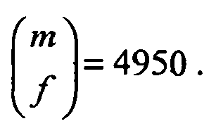


SCL 140 as described below. - An
SCL 140 for given parameters n, m, and f is designed as follows, with reference to the flowchart ofFig. 3 . - In
step 310, generate the set C of all bit-vectors of m bits wide that contain f ones and m-f zeros, and instep 320, construct matrix M from set C. The rows of matrix M are bit-vectors from set C. The vectors are chosen from C in such a way that the overlap between any two columns in matrix M is minimized. Details for thesteps - Set C contains all bit-vectors of m bits wide that contain f ones and m-f zeros. There are


- Matrix M is built from the rows in matrix Q. Let ni indicate the number of times that row i from matrix Q occurs in matrix M. Matrix M has n rows, and hence:

- Let qij indicate the element of matrix Q at row i and column j. Each column in matrix M should contain g ones and n-g zeros, and hence:


- The overlap between any two columns in matrix M should be minimized, and hence the number of times that a row from matrix Q occurs in matrix M should be minimized. A constraint is therefore to minimize max i=1...|C| ni . Since there are


- For f=1, the
SCL 140 has no spreadingnetwork 150 and consists of thecompaction network 160 only. In that case, each SCL input is connected to one SCL output, and hence each SCL output is connected to a distinct set of SCL inputs. - For f > 1, the overlap is minimized if


- In case of minimum overlap, it holds for the compaction ratio that


IC 100 on whichSCL 140 is to be placed, as previously explained. - An example of a design of an
SCL 140 with n=10, m=4, and f=2 using the design method of the present invention is given below. From the teachings of the method of the present invention, it follows that

- a) The set C of all bit-vector of 4 bits wide that contain 2 ones, has cardinality

- b) The system of m+1 = 5 equations in 6 unknowns is as follows:


- c) Since

Appropriate solutions therefore are:- Solution 1: n 1 = 1, n 2 = 2, n 3 = 2, n 4 = 2, n 5 = 2, n 6 = 1.
- Solution 2: n 1 = 2, n 2 = 1, n 3 = 2 , n 4 = 2 , n 5 = 1, n 6 = 2.
- Solution 3: n 1 = 2, n 2 = 2, n 3 = 1, n 4 = 1, n 5 = 2, n 6 = 2.

- d) The maximum overlap between the columns in matrix M is


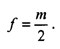
- The fault detection capabilities of an
SCL 140 according to the present invention are as follows: - A single fault is always detected if all rows in matrix M are not 0. For fanout f, the fault is observed at f SCL outputs.
- Two simultaneous faults are detected if all rows are distinct. The XOR (i.e. modulo-2 sum) of any two rows is then a vector that is not equal to 0.
- Any odd number of simultaneous faults is detected if the XOR (i.e. modulo-2 addition) of any odd number of rows results in a vector that is not equal to 0. This is achieved for instance in case the fanout f is odd. In that case, all rows contain an odd number of ones. The total number of ones in any odd number of rows, where each row contains an odd number of ones, is the product of two odd numbers, which always results in an odd number.
- Four or a higher even number of simultaneous faults may not be detected. However, the design of the
SCL 140 ensures that the probability for non-detection is minimized. - It should be noted that the above-mentioned embodiments illustrate rather than limit the invention, and that those skilled in the art will be able to design many alternative embodiments without departing from the scope of the appended claims. In the claims, any reference signs placed between parentheses shall not be construed as limiting the claim. The word "comprising" does not exclude the presence of elements or steps other than those listed in a claim. The word "a" or "an" preceding an element does not exclude the presence of a plurality of such elements. The invention can be implemented by means of hardware comprising several distinct elements. In the device claim enumerating several means, several of these means can be embodied by one and the same item of hardware. The mere fact that certain measures are recited in mutually different dependent claims does not indicate that a combination of these measures cannot be used to advantage.
Claims (11)
- Space compaction logic (140) for coupling an integrated circuit (200) having a plurality of digital outputs (210) to a test apparatus for testing the integrated circuit (200), each of the digital outputs being arranged to provide a test result in a test mode of the integrated circuit, the space compaction logic comprising a space compaction network (160),
the space compaction logic being characterized by:the space compaction network having a plurality of compaction domains (162), each domain being arranged to compact a plurality of test results into a further test result;and by further comprising:a spreading network (150) coupled between the plurality of digital outputs (210) and the space compaction network (160), the spreading network (150) being arranged to duplicate each test result from the digital outputs to a number of compaction domains (162). - Space compaction logic (280) as claimed in claim 1, wherein each compaction domain (162) comprises a network of exclusive logic gates.
- Space compaction logic (280) as claimed in claim 1 or 2, wherein each compaction domain (162) is arranged to be coupled to a unique set of digital outputs (210).
- An integrated circuit arrangement (10, 20) comprising:an integrated circuit (100, 200) comprising plurality of digital outputs (122, 210), each of the outputs being arranged to provide a test result in a test mode of the integrated circuit; andspace compaction logic (140) as claimed in any of claims 1-3.
- An integrated circuit arrangement (10, 20) as claimed in claim 4, wherein each compaction domain (162) has an output for producing its further test result, the integrated circuit further comprising a shift register (170) for serially shifting data towards a test data output (172) of the integrated circuit, the respective outputs of the compaction domains (162) being coupled to respective cells of the shift register (170).
- An integrated circuit arrangement (20) as claimed in claim 4 or 5, further comprising a test means including an automated test apparatus (220) and a load board (280) for coupling the integrated circuit to the test apparatus, the test means further comprising the space compaction logic (140).
- An integrated circuit arrangement (10, 20) as claimed in any of claims 4-6, wherein the spreading network (150) is configurably coupled to the digital outputs.
- A method for designing space compaction logic (140) for testing an integrated circuit (100, 200) having a plurality of digital outputs (122, 210), the space compaction logic (140) comprising:a space compaction network (160) having a plurality of compaction domains having m outputs, each domain being arranged to compact a plurality of test results into a further test result; anda spreading network (150) having n inputs for coupling between the plurality of digital outputs (122, 210) and the space compaction network, the spreading network being arranged to duplicate each test result from the digital outputs to f compaction domains, f, n and m being positive integers with n being larger than m, and m being larger than f, the method being characterized by comprising:generating (310) a set of bit vectors, each vector comprising m bits, each bit indicating the presence of a conductive path from an input of the spreading network to an output of the space compaction network, the total number of conductive paths per vector being f; andcombining (320) n vectors from the set of bit vectors into a matrix of size n*m, such that in a direction of the matrix perpendicular to the direction of the vectors the number of said conductive paths is limited, said matrix representing the space compaction logic design.
- A method as claimed in claim 8, wherein the step of combining n vectors from the set of bit vectors into a matrix of size n*m, such that in a direction of the matrix perpendicular to the direction of the vectors the number of conductive paths is limited comprises minimizing said number.
- A test apparatus (220) comprising:a plurality of inputs (222) for connecting to a plurality of digital outputs (210) of an integrated circuit (200), each of the digital outputs being arranged to provide a test result in a test mode of the integrated circuit; andspace compaction logic (140) as claimed in any of claims 1-3, wherein the spreading network (150) is coupled to the plurality of digital outputs via the plurality of inputs (222).
- An interface (280) comprising the space compaction logic as claimed in any of claims 1-3.
Priority Applications (1)
| Application Number | Priority Date | Filing Date | Title |
|---|---|---|---|
| EP06809673A EP1952168B1 (en) | 2005-11-14 | 2006-10-23 | Integrated circuit arrangement and design method |
Applications Claiming Priority (3)
| Application Number | Priority Date | Filing Date | Title |
|---|---|---|---|
| EP05110725 | 2005-11-14 | ||
| EP06809673A EP1952168B1 (en) | 2005-11-14 | 2006-10-23 | Integrated circuit arrangement and design method |
| PCT/IB2006/053895 WO2007054845A2 (en) | 2005-11-14 | 2006-10-23 | Integrated circuit arrangement and design method |
Publications (2)
| Publication Number | Publication Date |
|---|---|
| EP1952168A2 EP1952168A2 (en) | 2008-08-06 |
| EP1952168B1 true EP1952168B1 (en) | 2010-04-14 |
Family
ID=37946470
Family Applications (1)
| Application Number | Title | Priority Date | Filing Date |
|---|---|---|---|
| EP06809673A Not-in-force EP1952168B1 (en) | 2005-11-14 | 2006-10-23 | Integrated circuit arrangement and design method |
Country Status (8)
| Country | Link |
|---|---|
| US (1) | US7945828B2 (en) |
| EP (1) | EP1952168B1 (en) |
| JP (1) | JP2009516164A (en) |
| CN (1) | CN101310191B (en) |
| AT (1) | ATE464572T1 (en) |
| DE (1) | DE602006013690D1 (en) |
| TW (1) | TW200736629A (en) |
| WO (1) | WO2007054845A2 (en) |
Families Citing this family (6)
| Publication number | Priority date | Publication date | Assignee | Title |
|---|---|---|---|---|
| US20090150112A1 (en) * | 2007-12-05 | 2009-06-11 | Sun Microsystems, Inc. | Scan method and system of testing chip having multiple cores |
| US9523736B2 (en) * | 2014-06-19 | 2016-12-20 | Nuvoton Technology Corporation | Detection of fault injection attacks using high-fanout networks |
| CN104122497B (en) * | 2014-08-11 | 2016-09-21 | 中国科学院自动化研究所 | The generative circuit of test vector and method needed for integrated circuit built-in self-test |
| CN108872837B (en) * | 2018-08-28 | 2024-10-29 | 长鑫存储技术有限公司 | Data compression circuit, memory, integrated circuit testing device and testing method |
| CN111175635B (en) * | 2019-12-31 | 2021-12-03 | 中国电子产品可靠性与环境试验研究所((工业和信息化部电子第五研究所)(中国赛宝实验室)) | Integrated circuit testing device |
| TWI783555B (en) * | 2021-06-28 | 2022-11-11 | 瑞昱半導體股份有限公司 | Semiconductor device and method for generating test pulse signals |
Family Cites Families (3)
| Publication number | Priority date | Publication date | Assignee | Title |
|---|---|---|---|---|
| US7552373B2 (en) * | 2002-01-16 | 2009-06-23 | Syntest Technologies, Inc. | Method and apparatus for broadcasting scan patterns in a scan-based integrated circuit |
| US7243110B2 (en) * | 2004-02-20 | 2007-07-10 | Sand Technology Inc. | Searchable archive |
| US7308634B2 (en) * | 2005-04-01 | 2007-12-11 | Kabushiki Kaisha Toshiba | Systems and methods for LBIST testing using multiple functional subphases |
-
2006
- 2006-10-23 DE DE602006013690T patent/DE602006013690D1/en active Active
- 2006-10-23 WO PCT/IB2006/053895 patent/WO2007054845A2/en not_active Ceased
- 2006-10-23 AT AT06809673T patent/ATE464572T1/en not_active IP Right Cessation
- 2006-10-23 EP EP06809673A patent/EP1952168B1/en not_active Not-in-force
- 2006-10-23 US US12/093,639 patent/US7945828B2/en not_active Expired - Fee Related
- 2006-10-23 CN CN2006800423480A patent/CN101310191B/en not_active Expired - Fee Related
- 2006-10-23 JP JP2008539544A patent/JP2009516164A/en not_active Withdrawn
- 2006-11-10 TW TW095141800A patent/TW200736629A/en unknown
Also Published As
| Publication number | Publication date |
|---|---|
| WO2007054845A3 (en) | 2007-08-02 |
| TW200736629A (en) | 2007-10-01 |
| DE602006013690D1 (en) | 2010-05-27 |
| US20090024893A1 (en) | 2009-01-22 |
| CN101310191A (en) | 2008-11-19 |
| ATE464572T1 (en) | 2010-04-15 |
| CN101310191B (en) | 2011-04-20 |
| JP2009516164A (en) | 2009-04-16 |
| EP1952168A2 (en) | 2008-08-06 |
| WO2007054845A2 (en) | 2007-05-18 |
| US7945828B2 (en) | 2011-05-17 |
Similar Documents
| Publication | Publication Date | Title |
|---|---|---|
| Jarwala et al. | A new framework for analyzing test generation and diagnosis algorithms for wiring interconnects | |
| CN105631077B (en) | Integrated circuit with increased fault coverage | |
| US6385750B1 (en) | Method and system for controlling test data volume in deterministic test pattern generation | |
| US7343536B2 (en) | Scan based automatic test pattern generation (ATPG) test circuit, test method using the test circuit, and scan chain reordering method | |
| US7475317B2 (en) | Automatic test pattern generation | |
| US8898529B2 (en) | High performance compaction for test responses with many unknowns | |
| EP0329702A1 (en) | Programmable logic array | |
| US7185253B2 (en) | Compacting circuit responses | |
| US7415678B2 (en) | Method and apparatus for synthesis of multimode X-tolerant compressor | |
| US20220043062A1 (en) | Bidirectional scan cells for single-path reversible scan chains | |
| CN114667455A (en) | Universal compressor architecture for test circuits | |
| US7945828B2 (en) | Integrated circuit arrangement and design method | |
| US7818643B2 (en) | Method for blocking unknown values in output response of scan test patterns for testing circuits | |
| US9310431B2 (en) | Diagnosis framework to shorten yield learning cycles of advanced processes | |
| Niewenhuis et al. | Efficient built-in self test of regular logic characterization vehicles | |
| Jiang et al. | Increased detection of hard-to-detect stuck-at faults during scan shift | |
| Kim et al. | Hierarchical test compression for SOC designs | |
| EP1629291B1 (en) | Automatic test pattern generation | |
| Ubar et al. | Embedded fault diagnosis in digital systems with BIST | |
| Saab et al. | Extraction based verification method for off the shelf integrated circuits | |
| Ahmad | Constant error masking behavior of an internal exclusive-OR type signature analyzer due to the changed polynomial seeds | |
| US20240337693A1 (en) | X-Masking for In-System Deterministic Test | |
| Novák et al. | Test response compaction method with improved detection and diagnostic abilities | |
| Ajit et al. | Design and Performance Comparison of X-Masking Models in DFT Applications | |
| Xu et al. | Gate-level fault diagnosis for scan-based VLSI environment |
Legal Events
| Date | Code | Title | Description |
|---|---|---|---|
| PUAI | Public reference made under article 153(3) epc to a published international application that has entered the european phase |
Free format text: ORIGINAL CODE: 0009012 |
|
| 17P | Request for examination filed |
Effective date: 20080616 |
|
| AK | Designated contracting states |
Kind code of ref document: A2 Designated state(s): AT BE BG CH CY CZ DE DK EE ES FI FR GB GR HU IE IS IT LI LT LU LV MC NL PL PT RO SE SI SK TR |
|
| 17Q | First examination report despatched |
Effective date: 20090213 |
|
| GRAP | Despatch of communication of intention to grant a patent |
Free format text: ORIGINAL CODE: EPIDOSNIGR1 |
|
| GRAS | Grant fee paid |
Free format text: ORIGINAL CODE: EPIDOSNIGR3 |
|
| GRAA | (expected) grant |
Free format text: ORIGINAL CODE: 0009210 |
|
| AK | Designated contracting states |
Kind code of ref document: B1 Designated state(s): AT BE BG CH CY CZ DE DK EE ES FI FR GB GR HU IE IS IT LI LT LU LV MC NL PL PT RO SE SI SK TR |
|
| REG | Reference to a national code |
Ref country code: GB Ref legal event code: FG4D |
|
| REG | Reference to a national code |
Ref country code: CH Ref legal event code: EP |
|
| REG | Reference to a national code |
Ref country code: IE Ref legal event code: FG4D |
|
| REF | Corresponds to: |
Ref document number: 602006013690 Country of ref document: DE Date of ref document: 20100527 Kind code of ref document: P |
|
| REG | Reference to a national code |
Ref country code: NL Ref legal event code: VDEP Effective date: 20100414 |
|
| LTIE | Lt: invalidation of european patent or patent extension |
Effective date: 20100414 |
|
| PG25 | Lapsed in a contracting state [announced via postgrant information from national office to epo] |
Ref country code: LT Free format text: LAPSE BECAUSE OF FAILURE TO SUBMIT A TRANSLATION OF THE DESCRIPTION OR TO PAY THE FEE WITHIN THE PRESCRIBED TIME-LIMIT Effective date: 20100414 Ref country code: ES Free format text: LAPSE BECAUSE OF FAILURE TO SUBMIT A TRANSLATION OF THE DESCRIPTION OR TO PAY THE FEE WITHIN THE PRESCRIBED TIME-LIMIT Effective date: 20100725 Ref country code: NL Free format text: LAPSE BECAUSE OF FAILURE TO SUBMIT A TRANSLATION OF THE DESCRIPTION OR TO PAY THE FEE WITHIN THE PRESCRIBED TIME-LIMIT Effective date: 20100414 Ref country code: SE Free format text: LAPSE BECAUSE OF FAILURE TO SUBMIT A TRANSLATION OF THE DESCRIPTION OR TO PAY THE FEE WITHIN THE PRESCRIBED TIME-LIMIT Effective date: 20100414 |
|
| PG25 | Lapsed in a contracting state [announced via postgrant information from national office to epo] |
Ref country code: AT Free format text: LAPSE BECAUSE OF FAILURE TO SUBMIT A TRANSLATION OF THE DESCRIPTION OR TO PAY THE FEE WITHIN THE PRESCRIBED TIME-LIMIT Effective date: 20100414 Ref country code: SI Free format text: LAPSE BECAUSE OF FAILURE TO SUBMIT A TRANSLATION OF THE DESCRIPTION OR TO PAY THE FEE WITHIN THE PRESCRIBED TIME-LIMIT Effective date: 20100414 Ref country code: IS Free format text: LAPSE BECAUSE OF FAILURE TO SUBMIT A TRANSLATION OF THE DESCRIPTION OR TO PAY THE FEE WITHIN THE PRESCRIBED TIME-LIMIT Effective date: 20100814 Ref country code: FI Free format text: LAPSE BECAUSE OF FAILURE TO SUBMIT A TRANSLATION OF THE DESCRIPTION OR TO PAY THE FEE WITHIN THE PRESCRIBED TIME-LIMIT Effective date: 20100414 Ref country code: LV Free format text: LAPSE BECAUSE OF FAILURE TO SUBMIT A TRANSLATION OF THE DESCRIPTION OR TO PAY THE FEE WITHIN THE PRESCRIBED TIME-LIMIT Effective date: 20100414 |
|
| PG25 | Lapsed in a contracting state [announced via postgrant information from national office to epo] |
Ref country code: GR Free format text: LAPSE BECAUSE OF FAILURE TO SUBMIT A TRANSLATION OF THE DESCRIPTION OR TO PAY THE FEE WITHIN THE PRESCRIBED TIME-LIMIT Effective date: 20100715 Ref country code: PL Free format text: LAPSE BECAUSE OF FAILURE TO SUBMIT A TRANSLATION OF THE DESCRIPTION OR TO PAY THE FEE WITHIN THE PRESCRIBED TIME-LIMIT Effective date: 20100414 Ref country code: CY Free format text: LAPSE BECAUSE OF FAILURE TO SUBMIT A TRANSLATION OF THE DESCRIPTION OR TO PAY THE FEE WITHIN THE PRESCRIBED TIME-LIMIT Effective date: 20100602 |
|
| PG25 | Lapsed in a contracting state [announced via postgrant information from national office to epo] |
Ref country code: EE Free format text: LAPSE BECAUSE OF FAILURE TO SUBMIT A TRANSLATION OF THE DESCRIPTION OR TO PAY THE FEE WITHIN THE PRESCRIBED TIME-LIMIT Effective date: 20100414 Ref country code: PT Free format text: LAPSE BECAUSE OF FAILURE TO SUBMIT A TRANSLATION OF THE DESCRIPTION OR TO PAY THE FEE WITHIN THE PRESCRIBED TIME-LIMIT Effective date: 20100816 Ref country code: DK Free format text: LAPSE BECAUSE OF FAILURE TO SUBMIT A TRANSLATION OF THE DESCRIPTION OR TO PAY THE FEE WITHIN THE PRESCRIBED TIME-LIMIT Effective date: 20100414 |
|
| PLBE | No opposition filed within time limit |
Free format text: ORIGINAL CODE: 0009261 |
|
| STAA | Information on the status of an ep patent application or granted ep patent |
Free format text: STATUS: NO OPPOSITION FILED WITHIN TIME LIMIT |
|
| PG25 | Lapsed in a contracting state [announced via postgrant information from national office to epo] |
Ref country code: BE Free format text: LAPSE BECAUSE OF FAILURE TO SUBMIT A TRANSLATION OF THE DESCRIPTION OR TO PAY THE FEE WITHIN THE PRESCRIBED TIME-LIMIT Effective date: 20100414 Ref country code: CZ Free format text: LAPSE BECAUSE OF FAILURE TO SUBMIT A TRANSLATION OF THE DESCRIPTION OR TO PAY THE FEE WITHIN THE PRESCRIBED TIME-LIMIT Effective date: 20100414 Ref country code: RO Free format text: LAPSE BECAUSE OF FAILURE TO SUBMIT A TRANSLATION OF THE DESCRIPTION OR TO PAY THE FEE WITHIN THE PRESCRIBED TIME-LIMIT Effective date: 20100414 Ref country code: SK Free format text: LAPSE BECAUSE OF FAILURE TO SUBMIT A TRANSLATION OF THE DESCRIPTION OR TO PAY THE FEE WITHIN THE PRESCRIBED TIME-LIMIT Effective date: 20100414 |
|
| 26N | No opposition filed |
Effective date: 20110117 |
|
| PG25 | Lapsed in a contracting state [announced via postgrant information from national office to epo] |
Ref country code: IT Free format text: LAPSE BECAUSE OF FAILURE TO SUBMIT A TRANSLATION OF THE DESCRIPTION OR TO PAY THE FEE WITHIN THE PRESCRIBED TIME-LIMIT Effective date: 20100414 |
|
| PG25 | Lapsed in a contracting state [announced via postgrant information from national office to epo] |
Ref country code: MC Free format text: LAPSE BECAUSE OF NON-PAYMENT OF DUE FEES Effective date: 20101031 |
|
| REG | Reference to a national code |
Ref country code: CH Ref legal event code: PL |
|
| PG25 | Lapsed in a contracting state [announced via postgrant information from national office to epo] |
Ref country code: CH Free format text: LAPSE BECAUSE OF NON-PAYMENT OF DUE FEES Effective date: 20101031 Ref country code: LI Free format text: LAPSE BECAUSE OF NON-PAYMENT OF DUE FEES Effective date: 20101031 |
|
| PG25 | Lapsed in a contracting state [announced via postgrant information from national office to epo] |
Ref country code: IE Free format text: LAPSE BECAUSE OF NON-PAYMENT OF DUE FEES Effective date: 20101023 |
|
| REG | Reference to a national code |
Ref country code: GB Ref legal event code: 732E Free format text: REGISTERED BETWEEN 20120621 AND 20120627 |
|
| PG25 | Lapsed in a contracting state [announced via postgrant information from national office to epo] |
Ref country code: BG Free format text: LAPSE BECAUSE OF FAILURE TO SUBMIT A TRANSLATION OF THE DESCRIPTION OR TO PAY THE FEE WITHIN THE PRESCRIBED TIME-LIMIT Effective date: 20100414 Ref country code: HU Free format text: LAPSE BECAUSE OF FAILURE TO SUBMIT A TRANSLATION OF THE DESCRIPTION OR TO PAY THE FEE WITHIN THE PRESCRIBED TIME-LIMIT Effective date: 20101015 Ref country code: LU Free format text: LAPSE BECAUSE OF NON-PAYMENT OF DUE FEES Effective date: 20101023 |
|
| REG | Reference to a national code |
Ref country code: GB Ref legal event code: 732E Free format text: REGISTERED BETWEEN 20120927 AND 20121003 |
|
| PG25 | Lapsed in a contracting state [announced via postgrant information from national office to epo] |
Ref country code: TR Free format text: LAPSE BECAUSE OF FAILURE TO SUBMIT A TRANSLATION OF THE DESCRIPTION OR TO PAY THE FEE WITHIN THE PRESCRIBED TIME-LIMIT Effective date: 20100414 |
|
| PGFP | Annual fee paid to national office [announced via postgrant information from national office to epo] |
Ref country code: GB Payment date: 20120924 Year of fee payment: 7 |
|
| PGFP | Annual fee paid to national office [announced via postgrant information from national office to epo] |
Ref country code: FR Payment date: 20121115 Year of fee payment: 7 |
|
| PG25 | Lapsed in a contracting state [announced via postgrant information from national office to epo] |
Ref country code: BG Free format text: LAPSE BECAUSE OF FAILURE TO SUBMIT A TRANSLATION OF THE DESCRIPTION OR TO PAY THE FEE WITHIN THE PRESCRIBED TIME-LIMIT Effective date: 20100714 |
|
| PGFP | Annual fee paid to national office [announced via postgrant information from national office to epo] |
Ref country code: DE Payment date: 20130920 Year of fee payment: 8 |
|
| GBPC | Gb: european patent ceased through non-payment of renewal fee |
Effective date: 20131023 |
|
| PG25 | Lapsed in a contracting state [announced via postgrant information from national office to epo] |
Ref country code: GB Free format text: LAPSE BECAUSE OF NON-PAYMENT OF DUE FEES Effective date: 20131023 |
|
| REG | Reference to a national code |
Ref country code: FR Ref legal event code: ST Effective date: 20140630 |
|
| PG25 | Lapsed in a contracting state [announced via postgrant information from national office to epo] |
Ref country code: FR Free format text: LAPSE BECAUSE OF NON-PAYMENT OF DUE FEES Effective date: 20131031 |
|
| REG | Reference to a national code |
Ref country code: DE Ref legal event code: R119 Ref document number: 602006013690 Country of ref document: DE |
|
| PG25 | Lapsed in a contracting state [announced via postgrant information from national office to epo] |
Ref country code: DE Free format text: LAPSE BECAUSE OF NON-PAYMENT OF DUE FEES Effective date: 20150501 |