EP1947693B1 - Plane structure of light-emitting diode lighting apparatus - Google Patents
Plane structure of light-emitting diode lighting apparatus Download PDFInfo
- Publication number
- EP1947693B1 EP1947693B1 EP07100750.4A EP07100750A EP1947693B1 EP 1947693 B1 EP1947693 B1 EP 1947693B1 EP 07100750 A EP07100750 A EP 07100750A EP 1947693 B1 EP1947693 B1 EP 1947693B1
- Authority
- EP
- European Patent Office
- Prior art keywords
- light
- transparent
- lighting apparatus
- emitting diodes
- plane structure
- Prior art date
- Legal status (The legal status is an assumption and is not a legal conclusion. Google has not performed a legal analysis and makes no representation as to the accuracy of the status listed.)
- Not-in-force
Links
Images




Classifications
-
- H—ELECTRICITY
- H10—SEMICONDUCTOR DEVICES; ELECTRIC SOLID-STATE DEVICES NOT OTHERWISE PROVIDED FOR
- H10W—GENERIC PACKAGES, INTERCONNECTIONS, CONNECTORS OR OTHER CONSTRUCTIONAL DETAILS OF DEVICES COVERED BY CLASS H10
- H10W90/00—Package configurations
-
- B—PERFORMING OPERATIONS; TRANSPORTING
- B32—LAYERED PRODUCTS
- B32B—LAYERED PRODUCTS, i.e. PRODUCTS BUILT-UP OF STRATA OF FLAT OR NON-FLAT, e.g. CELLULAR OR HONEYCOMB, FORM
- B32B17/00—Layered products essentially comprising sheet glass, or glass, slag, or like fibres
- B32B17/06—Layered products essentially comprising sheet glass, or glass, slag, or like fibres comprising glass as the main or only constituent of a layer, next to another layer of a specific material
- B32B17/10—Layered products essentially comprising sheet glass, or glass, slag, or like fibres comprising glass as the main or only constituent of a layer, next to another layer of a specific material of synthetic resin
- B32B17/10005—Layered products essentially comprising sheet glass, or glass, slag, or like fibres comprising glass as the main or only constituent of a layer, next to another layer of a specific material of synthetic resin laminated safety glass or glazing
- B32B17/10009—Layered products essentially comprising sheet glass, or glass, slag, or like fibres comprising glass as the main or only constituent of a layer, next to another layer of a specific material of synthetic resin laminated safety glass or glazing characterized by the number, the constitution or treatment of glass sheets
- B32B17/10036—Layered products essentially comprising sheet glass, or glass, slag, or like fibres comprising glass as the main or only constituent of a layer, next to another layer of a specific material of synthetic resin laminated safety glass or glazing characterized by the number, the constitution or treatment of glass sheets comprising two outer glass sheets
-
- B—PERFORMING OPERATIONS; TRANSPORTING
- B32—LAYERED PRODUCTS
- B32B—LAYERED PRODUCTS, i.e. PRODUCTS BUILT-UP OF STRATA OF FLAT OR NON-FLAT, e.g. CELLULAR OR HONEYCOMB, FORM
- B32B17/00—Layered products essentially comprising sheet glass, or glass, slag, or like fibres
- B32B17/06—Layered products essentially comprising sheet glass, or glass, slag, or like fibres comprising glass as the main or only constituent of a layer, next to another layer of a specific material
- B32B17/10—Layered products essentially comprising sheet glass, or glass, slag, or like fibres comprising glass as the main or only constituent of a layer, next to another layer of a specific material of synthetic resin
- B32B17/10005—Layered products essentially comprising sheet glass, or glass, slag, or like fibres comprising glass as the main or only constituent of a layer, next to another layer of a specific material of synthetic resin laminated safety glass or glazing
- B32B17/1055—Layered products essentially comprising sheet glass, or glass, slag, or like fibres comprising glass as the main or only constituent of a layer, next to another layer of a specific material of synthetic resin laminated safety glass or glazing characterized by the resin layer, i.e. interlayer
- B32B17/10761—Layered products essentially comprising sheet glass, or glass, slag, or like fibres comprising glass as the main or only constituent of a layer, next to another layer of a specific material of synthetic resin laminated safety glass or glazing characterized by the resin layer, i.e. interlayer containing vinyl acetal
-
- B—PERFORMING OPERATIONS; TRANSPORTING
- B32—LAYERED PRODUCTS
- B32B—LAYERED PRODUCTS, i.e. PRODUCTS BUILT-UP OF STRATA OF FLAT OR NON-FLAT, e.g. CELLULAR OR HONEYCOMB, FORM
- B32B17/00—Layered products essentially comprising sheet glass, or glass, slag, or like fibres
- B32B17/06—Layered products essentially comprising sheet glass, or glass, slag, or like fibres comprising glass as the main or only constituent of a layer, next to another layer of a specific material
- B32B17/10—Layered products essentially comprising sheet glass, or glass, slag, or like fibres comprising glass as the main or only constituent of a layer, next to another layer of a specific material of synthetic resin
- B32B17/10005—Layered products essentially comprising sheet glass, or glass, slag, or like fibres comprising glass as the main or only constituent of a layer, next to another layer of a specific material of synthetic resin laminated safety glass or glazing
- B32B17/1055—Layered products essentially comprising sheet glass, or glass, slag, or like fibres comprising glass as the main or only constituent of a layer, next to another layer of a specific material of synthetic resin laminated safety glass or glazing characterized by the resin layer, i.e. interlayer
- B32B17/10788—Layered products essentially comprising sheet glass, or glass, slag, or like fibres comprising glass as the main or only constituent of a layer, next to another layer of a specific material of synthetic resin laminated safety glass or glazing characterized by the resin layer, i.e. interlayer containing ethylene vinylacetate
-
- F—MECHANICAL ENGINEERING; LIGHTING; HEATING; WEAPONS; BLASTING
- F21—LIGHTING
- F21S—NON-PORTABLE LIGHTING DEVICES; SYSTEMS THEREOF; VEHICLE LIGHTING DEVICES SPECIALLY ADAPTED FOR VEHICLE EXTERIORS
- F21S4/00—Lighting devices or systems using a string or strip of light sources
- F21S4/20—Lighting devices or systems using a string or strip of light sources with light sources held by or within elongate supports
-
- H—ELECTRICITY
- H05—ELECTRIC TECHNIQUES NOT OTHERWISE PROVIDED FOR
- H05K—PRINTED CIRCUITS; CASINGS OR CONSTRUCTIONAL DETAILS OF ELECTRIC APPARATUS; MANUFACTURE OF ASSEMBLAGES OF ELECTRICAL COMPONENTS
- H05K1/00—Printed circuits
- H05K1/02—Details
- H05K1/0274—Optical details, e.g. printed circuits comprising integral optical means
-
- F—MECHANICAL ENGINEERING; LIGHTING; HEATING; WEAPONS; BLASTING
- F21—LIGHTING
- F21Y—INDEXING SCHEME ASSOCIATED WITH SUBCLASSES F21K, F21L, F21S and F21V, RELATING TO THE FORM OR THE KIND OF THE LIGHT SOURCES OR OF THE COLOUR OF THE LIGHT EMITTED
- F21Y2115/00—Light-generating elements of semiconductor light sources
- F21Y2115/10—Light-emitting diodes [LED]
-
- H—ELECTRICITY
- H05—ELECTRIC TECHNIQUES NOT OTHERWISE PROVIDED FOR
- H05K—PRINTED CIRCUITS; CASINGS OR CONSTRUCTIONAL DETAILS OF ELECTRIC APPARATUS; MANUFACTURE OF ASSEMBLAGES OF ELECTRICAL COMPONENTS
- H05K1/00—Printed circuits
- H05K1/18—Printed circuits structurally associated with non-printed electric components
- H05K1/189—Printed circuits structurally associated with non-printed electric components characterised by the use of flexible or folded printed circuits
-
- H—ELECTRICITY
- H05—ELECTRIC TECHNIQUES NOT OTHERWISE PROVIDED FOR
- H05K—PRINTED CIRCUITS; CASINGS OR CONSTRUCTIONAL DETAILS OF ELECTRIC APPARATUS; MANUFACTURE OF ASSEMBLAGES OF ELECTRICAL COMPONENTS
- H05K2201/00—Indexing scheme relating to printed circuits covered by H05K1/00
- H05K2201/01—Dielectrics
- H05K2201/0104—Properties and characteristics in general
- H05K2201/0108—Transparent
-
- H—ELECTRICITY
- H05—ELECTRIC TECHNIQUES NOT OTHERWISE PROVIDED FOR
- H05K—PRINTED CIRCUITS; CASINGS OR CONSTRUCTIONAL DETAILS OF ELECTRIC APPARATUS; MANUFACTURE OF ASSEMBLAGES OF ELECTRICAL COMPONENTS
- H05K2201/00—Indexing scheme relating to printed circuits covered by H05K1/00
- H05K2201/03—Conductive materials
- H05K2201/032—Materials
- H05K2201/0326—Inorganic, non-metallic conductor, e.g. indium-tin oxide [ITO]
-
- H—ELECTRICITY
- H05—ELECTRIC TECHNIQUES NOT OTHERWISE PROVIDED FOR
- H05K—PRINTED CIRCUITS; CASINGS OR CONSTRUCTIONAL DETAILS OF ELECTRIC APPARATUS; MANUFACTURE OF ASSEMBLAGES OF ELECTRICAL COMPONENTS
- H05K2201/00—Indexing scheme relating to printed circuits covered by H05K1/00
- H05K2201/10—Details of components or other objects attached to or integrated in a printed circuit board
- H05K2201/10007—Types of components
- H05K2201/10106—Light emitting diode [LED]
-
- H—ELECTRICITY
- H10—SEMICONDUCTOR DEVICES; ELECTRIC SOLID-STATE DEVICES NOT OTHERWISE PROVIDED FOR
- H10H—INORGANIC LIGHT-EMITTING SEMICONDUCTOR DEVICES HAVING POTENTIAL BARRIERS
- H10H20/00—Individual inorganic light-emitting semiconductor devices having potential barriers, e.g. light-emitting diodes [LED]
- H10H20/80—Constructional details
- H10H20/85—Packages
- H10H20/857—Interconnections, e.g. lead-frames, bond wires or solder balls
-
- H—ELECTRICITY
- H10—SEMICONDUCTOR DEVICES; ELECTRIC SOLID-STATE DEVICES NOT OTHERWISE PROVIDED FOR
- H10W—GENERIC PACKAGES, INTERCONNECTIONS, CONNECTORS OR OTHER CONSTRUCTIONAL DETAILS OF DEVICES COVERED BY CLASS H10
- H10W72/00—Interconnections or connectors in packages
- H10W72/071—Connecting or disconnecting
- H10W72/072—Connecting or disconnecting of bump connectors
- H10W72/07251—Connecting or disconnecting of bump connectors characterised by changes in properties of the bump connectors during connecting
-
- H—ELECTRICITY
- H10—SEMICONDUCTOR DEVICES; ELECTRIC SOLID-STATE DEVICES NOT OTHERWISE PROVIDED FOR
- H10W—GENERIC PACKAGES, INTERCONNECTIONS, CONNECTORS OR OTHER CONSTRUCTIONAL DETAILS OF DEVICES COVERED BY CLASS H10
- H10W72/00—Interconnections or connectors in packages
- H10W72/20—Bump connectors, e.g. solder bumps or copper pillars; Dummy bumps; Thermal bumps
Definitions
- the present invention relates to a plane structure of a lighting apparatus and more especially, relates to a plane structure of a light-emitting diode lighting apparatus.
- LED light-emitting diode
- a lighting system with light-emitting diode may present effects on the varieties of color light not only to provide the function of ambient lighting but also to generate colorful enrichment with low power consumption.
- the application of light-emitting diode is provided generally with light-emitting diodes associated with the layout of circuit fixed or attached onto a hard and opaque carrier, which limits the size, dimensions, shape and viewing effect for an applied product.
- EP 1 437 215 A discloses a planar light-emitting diode lighting apparatus comprising a PET film, on which an electrically conductive pattern is formed connecting a plurality of LED packages, which are glued onto said PET film, the assembly being sandwiched between two glass plates.
- WO 2005/099310 A and EP 1 445 804 A both disclose LEDs having electrodes on opposite sides, which are electrically connected to two different transparent flexible sheets, which both carry contact patterns and sandwich a plurality of such LEDs.
- FR 2 812 071 A1 discloses a parallel connection of a plurality of LEDs, wherein a transparent flexible sheet carries two parallel conductor strips, which are optionally transparent. On one of the two strips the LEDs are mounted in a row and one electrode of each LED is electrically connected to that strip, while the second electrode of each LED is connected to the second conductor strip by a wire.
- one object of the present invention provides a plane structure of light-emitting diodes lighting apparatus.
- One or more light-emitting diodes are attached on a plane of flexible material and electrically connected via a specialized transparent pattern of the flexible material plane, which may be applied to decorate the furniture, the glass door, the glass window and interior design to prettify the scenery.
- Another object of this invention is to provide a plane structure of light-emitting diode lighting apparatus.
- Conductive material and insulating pattern are formed on a flexible tape, which may stack one layer or multiple layers of light-emitting diodes to diversify the light-emitting diodes deployment and enhance the stereo design to improve effect of prettification and diversion.
- the present invention provides plane structure of a light-emitting diode lighting apparatus, comprising:a transparent flexible tape; an electrically conductive transparent pattern and an electrically insulating transparent pattern disposed on said transparent flexible tape, wherein said conductive transparent pattern is divided into a first zone and a second zone in the same plane by said insulating transparent pattern, and said first zone comprises a plurality of first discontinuous blocks electrically connected to an exterior first electrode and said second zone comprises a plurality of second discontinuous blocks electrically connected to an exterior second electrode; the first and second discontinuous blocks being divided by the electrically insulating transparent pattern; and a plurality of light-emitting diodes on said transparent flexible tape, wherein each of said light-emitting diodes has a positive electrode fixed on one of said first blocks and a negative electrode fixed on one of said second blocks.
- FIG. 1A is a cross-sectional diagram of a plane structure of an LED lighting apparatus in accordance with a first example of the present invention.
- An light-emitting diodes lighting apparatus includes a first transparent pattern and a second transparent pattern 120 on a transparent flexible tape 100.
- One or more first light-emitting diodes 130 are attached to the first transparent pattern with adhesive structures 131.
- the transparent flexible tape 100 is made of insulating and flexible material, such as poly (ethylene terephthalate) (PET), poly carbonate (PC), oriented polypropylene (OPP), poly vinylchlorid (PVC), acrylic or other polymer material, but not limited to.
- the first transparent pattern such as a first transparent conductive line 110, but not limited to, is made of such as ITO (Indium Tin Oxide), IZO (Indium Zinc Oxide), or acrylic transparent conductive gel, which is formed on the transparent flexible tape 100 by silk screening or printing. It is appreciated that the first transparent conductive line 110 may be dyed for visual arts.
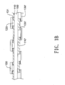
- the first transparent pattern further includes a first transparent conductive line 110' positioned on the other surface of the transparent flexible tape 100, and one or more first light-emitting diodes 130' are attached to the first transparent conductive line 110' with adhesive structures 131', wherein the first light-emitting diodes 130 and 130' are interlaced so as to decrease the pitch between the first light-emitting diodes 130 and 130' and, furthermore, to increase flexibility of the designs of the lighting apparatus.
- the forming method of the first transparent conductive lines 110' is the same as that mentioned in the first example
- the first transparent conductive line 110 or 110' has a plurality of discontinuous conductive lines 1101 separated by the second transparent pattern 120, wherein the first transparent conductive line 110 is electrically insulated from the second transparent pattern 120.
- the second transparent pattern 120 is constituted by one surface of the transparent flexible tape.
- the second transparent pattern 120 may be constituted by an insulating material which is formed on the surface of the transparent flexible tape.
- each light-emitting diode 130 is electrically connected across two ends of the conductive lines 1101.
- one end of the conductive line 1101 is electrically connected to one or more exterior positive electrodes (not shown) and the other end to one or more exterior negative electrode (not shown), so as to electrically connect the light-emitting diodes 130 to an exterior power supply which provides power to the light-emitting diodes 130 by one or more sets of positive and negative power wires.
- the first transparent conductive line 110 may be electrically connected to exterior control lines for controlling the performance of light-emitting diodes 130.
- the light-emitting diodes 130 may be a monochromatic light-emitting diode or polychromatic light-emitting diode, which are not limited to one type.
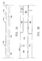
- FIG. 2A is a cross-sectional diagram illustrating the plane structure of the light-emitting diode lighting apparatus in accordance with a first embodiment of the present invention.
- a first transparent pattern is disposed on a transparent flexible tape 400, and, in this embodiment, the first transparent pattern is a transparent conductive film 420, which is divided into a first zone 460 and a second zone 470 by a second transparent pattern 410.
- the transparent conductive film 420 not limited to, is made of transparent conductive material such as ITO or IZO, which is formed on the transparent flexible tape 400 by sputtering, evaporate plating, printing or attaching.
- the transparent conductive film 420 may be made with a conductive material implanted a dye or dyes for visual arts.
- the second transparent pattern 410 will be formed on the transparent conductive film 420 as an insulating pattern by a suitable method, such as laser, chemically etching, printing or cutting, to make the first zone 460 and the second zone 470 electrically insulating from each other.
- FIG. 2B is a cross-sectional diagram illustrating one side of the plane structure of the light-emitting diodes lighting apparatus in accordance with FIG. 2A .
- the first transparent pattern includes the first zone 460 and the second zone 470, and the first zone 460 and the second zone 470 have some discontinuous blocks divided by the second transparent pattern 410.
- all first blocks of the first zone 460 may electrically or physically be connected to one or more first exterior electrodes (in this embodiment, the first exterior electrodes are positive electrodes).
- all second blocks of the second zone 470 may electrically or physically be connected to one or more second exterior electrodes which are different from the first exterior electrodes (in this embodiment, the second exterior electrodes are negative electrodes).
- each light-emitting diode 430 is attached across the second transparent pattern 410, wherein each light-emitting diode 430 has a positive electrode fixed on one first block of the first zone 460 and a negative electrode fixed on one second block of the second zone 470. Accordingly,
- the first zone 460 may be connected to one or more exterior positive electrodes, as well as the second zone 470 to one or more exterior negative electrodes.
- the light-emitting diode lighting apparatus can be evolved as a double-side light-emitting diode lighting apparatus by forming another first transparent pattern and another second transparent pattern on the other surface of the transparent flexible tape. That is, the first transparent patterns of both sides of the transparent flexible tape are made of conductive material. Besides, the conductive material may be selected from the groups consisted of transparent acrylic conductive gel, indium tin oxide, and indium zinc oxide. And, the second transparent pattern includes at least one of the surfaces of the transparent flexible tape or an insulation layer.
- the only criterion to establish such a double-side light-emitting diode lighting apparatus is that all light-emitting diodes on both sides of the lighting apparatus have to overlapped across positioned, as this result, the light-emitting diodes lighting apparatus can display the visual arts.
- FIG. 3 is a cross-sectional diagram of the plane structure of the light-emitting diode lighting apparatus in accordance with a third example.
- a first transparent pattern is positioned on a transparent flexible tape 300, wherein the first transparent pattern is a plurality of first transparent conductive lines 310 in this embodiment, but not limited to.
- the second transparent pattern further includes a patterned insulation layer 340 disposed on the first transparent conductive lines 310, but two ends of the first transparent conductive lines 310 and the places which are going to place the first light-emitting diodes 330 are exposed out of the patterned insulation layer 340. The exposed ends of the first transparent conductive lines 310 are connected to a plurality of first light-emitting diodes 330.
- the first transparent pattern further includes a plurality of second transparent conductive lines 350 on the patterned insulation layer 340.
- the layout of the second transparent conductive lines 350 may be overlapped across the first transparent conductive lines 310.
- a plurality of second light-emitting diodes 360 is attached and electrically connected to the second transparent conductive lines 350.
- the first transparent pattern is the first transparent conductive line 310 or the combination of the first transparent conductive line 310 and the second transparent conductive line 350 thereof, but not limited to, and the first transparent pattern can also be a transparent conductive film, which is aforementioned on the first embodiment.
- another plane structure of the light-emitting diodes lighting apparatus form which is the same as the previous example, may also be formed on the other surface of the transparent flexible tape 300 to establish a double-side, multi-storey light-emitting diodes lighting apparatus.
- the only criterion to establish such a double-side, multi-storey light-emitting diodes lighting apparatus is that all light-emitting diodes of the lighting apparatus have to overlapped across positioned, as this result, the light-emitting diodes lighting apparatus can display the visual arts.
- one or more layers of light-emitting diodes may be stacked on one or both sides of a flexible plane structure with light-emitting diodes to enhance various applications.
- the plane structure of LED lighting apparatus may have the light-emitting diodes in various amounts, sizes or kinds, such as monochromatic or polychromatic light-emitting diodes, in order to provide flexibility on designs.
- the carrier of the light-emitting diodes made of flexible tape may be cut in various sizes and shapes, and, even more, the done plane structure of light-emitting diodes lighting apparatus may be positioned on a given shape or size carrier, such as a curve carrier, to meet with different designs.
- the plane structure of light-emitting diodes lighting apparatus in accordance with the present invention may be applied to indoor/outdoor partition, furniture, table, ceiling, shower partition, glass wall, display window, specific light stand, table decoration, advertisement or display panel, but not limited to.
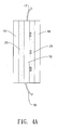
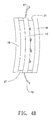
- FIG. 4A and FIG. 4B are the side elevation view of a lighting apparatus in accordance with an embodiment of the present invention.
- the lighting apparatus 10 is inserted between two transparent rigid substrates 16 and 18 to form a light-emitting diodes peripheral product.
- the lighting apparatus 10 includes a power line 17 and a ground line 19, which are exposed out of the lighting apparatus 10, and an interlayer film 21, which is filled into the space between the lighting apparatus and two transparent rigid substrates 16 or 18 to protect light-emitting diodes.
- the interlayer film 21 is made of poly vinyl butyral (PVB), EN, polyethylenenapthalate (PEN), ethyl vinyl acetate (EVA), or gel, but not limited to.
- the material of the transparent rigid substrate 16 and 18 can be glass, polycarbonate, plastic, laminated glass or laminated plastic, but not limited to.
- the interlayer film 21 may be distributed over the plane structure of light-emitting diodes lighting apparatus (as shown in FIG. 4A ) or the periphery of the lighting apparatus 10 (as shown in FIG. 4B ).
- FIG. 5 is a flowchart illustrating the formation of the plane structure of the light-emitting diodes lighting apparatus in accordance with an embodiment of the present invention.
- a flexible tape is provided (step 20), and a transparent conductive film is formed on one or two sides of the flexible tape by any suitable method (step 22), such as sputtering, evaporate plating, printing, coating or film attaching.
- an insulating pattern is done on the transparent conductive film in laser cutting, chemical etching or cutting (step 24).
- the insulating pattern may include some lines to divide the transparent conductive film into some blocks, but not limited to the lines in the present invention.
- Some adhesive structures are formed on the pre-determined positions of the transparent conductive film (step 26), such as some conductive adhesive pads, which are formed by dipping method.
- light-emitting diodes are attached on the adhesive structures (step 28).
- the dipping method is also employed to form conductive adhesive points directly on the pins of every light-emitting diodes, such as silver gel or solder on the pins, and then light-emitting diodes can be attached on the transparent conductive film.
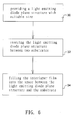
- FIG. 6 is a flowchart illustrating the formation of the plane structure of the light-emitting diodes lighting apparatus in accordance with another embodiment of the present invention.
- the plane structure of the present invention may be fixed on any suitable substrate.
- the plane structure of light-emitting diodes lighting apparatus according to the process shown in FIG. 1A may be cut into various sizes for different designs to provide coming assembly (step 30). It is understood that a flexible tape in any shape may be provided before the manufacture of the plane structure of light-emitting diodes lighting apparatus.
- the plane structure of light-emitting diodes lighting apparatus may be inserted between two substrates (step 32), such as two transparent rigid glass substrates.
- Interlayer film is filled into the space between the plane structure of light-emitting diodes lighting apparatus and each substrate to protect light-emitting diodes (step 34).
- the interlayer film may be distributed on the periphery of the plane structure of light-emitting diodes lighting apparatus or over the plane structure of light-emitting diodes lighting apparatus.
- the interlayer film may be coated on a first substrate before the plane structure of light-emitting diodes lighting apparatus is positioned. Then the interlayer film (or the other) is coated on the plane structure on light-emitting diodes lighting apparatus and then covered with a second substrate.
Landscapes
- Engineering & Computer Science (AREA)
- General Engineering & Computer Science (AREA)
- Microelectronics & Electronic Packaging (AREA)
- Led Device Packages (AREA)
- Fastening Of Light Sources Or Lamp Holders (AREA)
Description
- The present invention relates to a plane structure of a lighting apparatus and more especially, relates to a plane structure of a light-emitting diode lighting apparatus.
- With the development and progress of the technology, light-emitting diode (LED) plays an important role on various application due to its low thermal dissipation, low power consumption, long life, quick response, small volume, good vibration resistance, no gas discharge and plate package. Thus, light-emitting diode may be applied on the products of lighting, prospect design, transportation instruction and electric display.
- For example, on the application of prospect beautification, a lighting system with light-emitting diode may present effects on the varieties of color light not only to provide the function of ambient lighting but also to generate colorful enrichment with low power consumption. However, the application of light-emitting diode is provided generally with light-emitting diodes associated with the layout of circuit fixed or attached onto a hard and opaque carrier, which limits the size, dimensions, shape and viewing effect for an applied product.
-
EP 1 437 215 A discloses a planar light-emitting diode lighting apparatus comprising a PET film, on which an electrically conductive pattern is formed connecting a plurality of LED packages, which are glued onto said PET film, the assembly being sandwiched between two glass plates. -
WO 2005/099310 A andEP 1 445 804 A both disclose LEDs having electrodes on opposite sides, which are electrically connected to two different transparent flexible sheets, which both carry contact patterns and sandwich a plurality of such LEDs. -
FR 2 812 071 A1 - According to the issue mentioned previously, one object of the present invention provides a plane structure of light-emitting diodes lighting apparatus. One or more light-emitting diodes are attached on a plane of flexible material and electrically connected via a specialized transparent pattern of the flexible material plane, which may be applied to decorate the furniture, the glass door, the glass window and interior design to prettify the scenery.
- Another object of this invention is to provide a plane structure of light-emitting diode lighting apparatus. Conductive material and insulating pattern are formed on a flexible tape, which may stack one layer or multiple layers of light-emitting diodes to diversify the light-emitting diodes deployment and enhance the stereo design to improve effect of prettification and diversion.
- Accordingly, the present invention provides plane structure of a light-emitting diode lighting apparatus, comprising:a transparent flexible tape; an electrically conductive transparent pattern and an electrically insulating transparent pattern disposed on said transparent flexible tape, wherein said conductive transparent pattern is divided into a first zone and a second zone in the same plane by said insulating transparent pattern, and said first zone comprises a plurality of first discontinuous blocks electrically connected to an exterior first electrode and said second zone comprises a plurality of second discontinuous blocks electrically connected to an exterior second electrode; the first and second discontinuous blocks being divided by the electrically insulating transparent pattern; and a plurality of light-emitting diodes on said transparent flexible tape, wherein each of said light-emitting diodes has a positive electrode fixed on one of said first blocks and a negative electrode fixed on one of said second blocks.
- Other advantages of the present invention will become apparent from the following description taken in conjunction with the accompanying drawings wherein are set forth, by way of illustration and example, certain embodiments of the present invention.
- The foregoing aspects and many of the accompanying advantages of this invention will become more readily appreciated as the same becomes better understood by reference to the following detailed description, when taken in conjunction with the accompanying drawings, wherein:
-
FIG. 1A is a cross-sectional diagram of a plane structure of an light-emitting diode lighting apparatus in accordance with a first example -
FIG. 1B is a cross-sectional diagram of a plane structure of an light-emitting diodes lighting apparatus in accordance with a second example -
FIG. 1C is a front elevation view of one side of the plane structure of the light-emitting diodes lighting apparatus in accordance withFIG. 1A andFIG. 1B ; -
FIG. 2A is a cross-sectional diagram illustrating the plane structure of the light-emitting diodes lighting apparatus in accordance with a first embodiment of the present invention; -
FIG. 2B is a cross-sectional diagram illustrating one side of the plane structure of the light-emitting diodes lighting apparatus in accordance withFIG. 2A ; -
FIG. 3 is a cross-sectional diagram of the plane structure of the light-emitting diode lighting apparatus in accordance with a third example of the present invention; -
FIG. 4A andFIG. 4B are the side elevation view of a lighting apparatus in accordance with an embodiment of the present invention; -
FIG. 5 is a flowchart illustrating the formation of the plane structure of the light-emitting diodes lighting apparatus in accordance with an embodiment of the present invention; and -
FIG. 6 is a flowchart illustrating the formation of the plane structure of the light-emitting diodes lighting apparatus in accordance with another embodiment of the present invention. - The embodiments of the present invention are illustrated in reference to the drawings.
-
FIG. 1A is a cross-sectional diagram of a plane structure of an LED lighting apparatus in accordance with a first example of the present invention. An light-emitting diodes lighting apparatus includes a first transparent pattern and a secondtransparent pattern 120 on a transparentflexible tape 100. One or more first light-emitting diodes 130 are attached to the first transparent pattern withadhesive structures 131. In one example the transparentflexible tape 100 is made of insulating and flexible material, such as poly (ethylene terephthalate) (PET), poly carbonate (PC), oriented polypropylene (OPP), poly vinylchlorid (PVC), acrylic or other polymer material, but not limited to. Next, the first transparent pattern, such as a first transparentconductive line 110, but not limited to, is made of such as ITO (Indium Tin Oxide), IZO (Indium Zinc Oxide), or acrylic transparent conductive gel, which is formed on the transparentflexible tape 100 by silk screening or printing. It is appreciated that the first transparentconductive line 110 may be dyed for visual arts. - Referring to
FIG. 1B , is a cross-sectional diagram of a plane structure of an light-emitting diode lighting apparatus in accordance with a second example of the present invention. In the example the first transparent pattern further includes a first transparent conductive line 110' positioned on the other surface of the transparentflexible tape 100, and one or more first light-emitting diodes 130' are attached to the first transparent conductive line 110' with adhesive structures 131', wherein the first light-emitting diodes 130 and 130' are interlaced so as to decrease the pitch between the first light-emitting diodes 130 and 130' and, furthermore, to increase flexibility of the designs of the lighting apparatus. It is understood that the forming method of the first transparent conductive lines 110' is the same as that mentioned in the first example - As shown in
FIG. 1C presenting the front elevation view ofFIG. 1A orFIG. 1B , the first transparentconductive line 110 or 110' has a plurality of discontinuousconductive lines 1101 separated by the secondtransparent pattern 120, wherein the first transparentconductive line 110 is electrically insulated from the secondtransparent pattern 120. The secondtransparent pattern 120 is constituted by one surface of the transparent flexible tape. Alternatively, the secondtransparent pattern 120 may be constituted by an insulating material which is formed on the surface of the transparent flexible tape. In the example, each light-emitting diode 130 is electrically connected across two ends of theconductive lines 1101. Accordingly, one end of theconductive line 1101 is electrically connected to one or more exterior positive electrodes (not shown) and the other end to one or more exterior negative electrode (not shown), so as to electrically connect the light-emitting diodes 130 to an exterior power supply which provides power to the light-emittingdiodes 130 by one or more sets of positive and negative power wires. In addition to the connection of exterior power, the first transparentconductive line 110 may be electrically connected to exterior control lines for controlling the performance of light-emitting diodes 130. Accordingly, the light-emittingdiodes 130 may be a monochromatic light-emitting diode or polychromatic light-emitting diode, which are not limited to one type. -
FIG. 2A is a cross-sectional diagram illustrating the plane structure of the light-emitting diode lighting apparatus in accordance with a first embodiment of the present invention. A first transparent pattern is disposed on a transparentflexible tape 400, and, in this embodiment, the first transparent pattern is a transparentconductive film 420, which is divided into afirst zone 460 and asecond zone 470 by a secondtransparent pattern 410. In the embodiment, the transparentconductive film 420, not limited to, is made of transparent conductive material such as ITO or IZO, which is formed on the transparentflexible tape 400 by sputtering, evaporate plating, printing or attaching. It is understood that the transparentconductive film 420 may be made with a conductive material implanted a dye or dyes for visual arts. Next, the secondtransparent pattern 410 will be formed on the transparentconductive film 420 as an insulating pattern by a suitable method, such as laser, chemically etching, printing or cutting, to make thefirst zone 460 and thesecond zone 470 electrically insulating from each other. -
FIG. 2B is a cross-sectional diagram illustrating one side of the plane structure of the light-emitting diodes lighting apparatus in accordance withFIG. 2A . The first transparent pattern includes thefirst zone 460 and thesecond zone 470, and thefirst zone 460 and thesecond zone 470 have some discontinuous blocks divided by the secondtransparent pattern 410. Next, all first blocks of thefirst zone 460 may electrically or physically be connected to one or more first exterior electrodes (in this embodiment, the first exterior electrodes are positive electrodes). Similarly, all second blocks of thesecond zone 470 may electrically or physically be connected to one or more second exterior electrodes which are different from the first exterior electrodes (in this embodiment, the second exterior electrodes are negative electrodes). Furthermore, one or more light-emittingdiodes 430 are attached across the secondtransparent pattern 410, wherein each light-emittingdiode 430 has a positive electrode fixed on one first block of thefirst zone 460 and a negative electrode fixed on one second block of thesecond zone 470. Accordingly, - the
first zone 460 may be connected to one or more exterior positive electrodes, as well as thesecond zone 470 to one or more exterior negative electrodes. - It is understood, the light-emitting diode lighting apparatus can be evolved as a double-side light-emitting diode lighting apparatus by forming another first transparent pattern and another second transparent pattern on the other surface of the transparent flexible tape. That is, the first transparent patterns of both sides of the transparent flexible tape are made of conductive material. Besides, the conductive material may be selected from the groups consisted of transparent acrylic conductive gel, indium tin oxide, and indium zinc oxide. And, the second transparent pattern includes at least one of the surfaces of the transparent flexible tape or an insulation layer. And the only criterion to establish such a double-side light-emitting diode lighting apparatus is that all light-emitting diodes on both sides of the lighting apparatus have to overlapped across positioned, as this result, the light-emitting diodes lighting apparatus can display the visual arts.
-
FIG. 3 is a cross-sectional diagram of the plane structure of the light-emitting diode lighting apparatus in accordance with a third example. - A first transparent pattern is positioned on a transparent
flexible tape 300, wherein the first transparent pattern is a plurality of first transparentconductive lines 310 in this embodiment, but not limited to. For the difference between this example and the aforementioned examples and embodiments, the second transparent pattern further includes a patternedinsulation layer 340 disposed on the first transparentconductive lines 310, but two ends of the first transparentconductive lines 310 and the places which are going to place the first light-emittingdiodes 330 are exposed out of the patternedinsulation layer 340. The exposed ends of the first transparentconductive lines 310 are connected to a plurality of first light-emittingdiodes 330. Next, in addition to the first transparentconductive lines 310, the first transparent pattern further includes a plurality of second transparentconductive lines 350 on the patternedinsulation layer 340. The layout of the second transparentconductive lines 350 may be overlapped across the first transparentconductive lines 310. A plurality of second light-emittingdiodes 360 is attached and electrically connected to the second transparentconductive lines 350. In the example, the first transparent pattern is the first transparentconductive line 310 or the combination of the first transparentconductive line 310 and the second transparentconductive line 350 thereof, but not limited to, and the first transparent pattern can also be a transparent conductive film, which is aforementioned on the first embodiment. It is understood that another plane structure of the light-emitting diodes lighting apparatus form, which is the same as the previous example, may also be formed on the other surface of the transparentflexible tape 300 to establish a double-side, multi-storey light-emitting diodes lighting apparatus. And the only criterion to establish such a double-side, multi-storey light-emitting diodes lighting apparatus is that all light-emitting diodes of the lighting apparatus have to overlapped across positioned, as this result, the light-emitting diodes lighting apparatus can display the visual arts. - Accordingly, one or more layers of light-emitting diodes may be stacked on one or both sides of a flexible plane structure with light-emitting diodes to enhance various applications.
- Accordingly, the plane structure of LED lighting apparatus may have the light-emitting diodes in various amounts, sizes or kinds, such as monochromatic or polychromatic light-emitting diodes, in order to provide flexibility on designs. Next, the carrier of the light-emitting diodes made of flexible tape may be cut in various sizes and shapes, and, even more, the done plane structure of light-emitting diodes lighting apparatus may be positioned on a given shape or size carrier, such as a curve carrier, to meet with different designs. Thus, the plane structure of light-emitting diodes lighting apparatus in accordance with the present invention may be applied to indoor/outdoor partition, furniture, table, ceiling, shower partition, glass wall, display window, specific light stand, table decoration, advertisement or display panel, but not limited to.
- Please refer to
FIG. 4A andFIG. 4B , are the side elevation view of a lighting apparatus in accordance with an embodiment of the present invention. Thelighting apparatus 10 is inserted between two transparentrigid substrates lighting apparatus 10 includes apower line 17 and aground line 19, which are exposed out of thelighting apparatus 10, and aninterlayer film 21, which is filled into the space between the lighting apparatus and two transparentrigid substrates interlayer film 21 is made of poly vinyl butyral (PVB), EN, polyethylenenapthalate (PEN), ethyl vinyl acetate (EVA), or gel, but not limited to. And the material of the transparentrigid substrate interlayer film 21 may be distributed over the plane structure of light-emitting diodes lighting apparatus (as shown inFIG. 4A ) or the periphery of the lighting apparatus 10 (as shown inFIG. 4B ). -
FIG. 5 is a flowchart illustrating the formation of the plane structure of the light-emitting diodes lighting apparatus in accordance with an embodiment of the present invention. A flexible tape is provided (step 20), and a transparent conductive film is formed on one or two sides of the flexible tape by any suitable method (step 22), such as sputtering, evaporate plating, printing, coating or film attaching. Next, an insulating pattern is done on the transparent conductive film in laser cutting, chemical etching or cutting (step 24). In one embodiment, the insulating pattern may include some lines to divide the transparent conductive film into some blocks, but not limited to the lines in the present invention. Some adhesive structures are formed on the pre-determined positions of the transparent conductive film (step 26), such as some conductive adhesive pads, which are formed by dipping method. Next, light-emitting diodes are attached on the adhesive structures (step 28). Alternatively, the dipping method is also employed to form conductive adhesive points directly on the pins of every light-emitting diodes, such as silver gel or solder on the pins, and then light-emitting diodes can be attached on the transparent conductive film. -
FIG. 6 is a flowchart illustrating the formation of the plane structure of the light-emitting diodes lighting apparatus in accordance with another embodiment of the present invention. The plane structure of the present invention may be fixed on any suitable substrate. In another example, the plane structure of light-emitting diodes lighting apparatus according to the process shown inFIG. 1A may be cut into various sizes for different designs to provide coming assembly (step 30). It is understood that a flexible tape in any shape may be provided before the manufacture of the plane structure of light-emitting diodes lighting apparatus. Next, the plane structure of light-emitting diodes lighting apparatus may be inserted between two substrates (step 32), such as two transparent rigid glass substrates. Interlayer film is filled into the space between the plane structure of light-emitting diodes lighting apparatus and each substrate to protect light-emitting diodes (step 34). The interlayer film may be distributed on the periphery of the plane structure of light-emitting diodes lighting apparatus or over the plane structure of light-emitting diodes lighting apparatus. Alternatively, the interlayer film may be coated on a first substrate before the plane structure of light-emitting diodes lighting apparatus is positioned. Then the interlayer film (or the other) is coated on the plane structure on light-emitting diodes lighting apparatus and then covered with a second substrate. - Although the present invention has been explained in relation to its preferred embodiment, it is to be understood that other modifications and variation can be made without departing the scope of the invention as hereafter claimed.
Claims (4)
- A plane structure of a light-emitting diode lighting apparatus, comprising:a transparent flexible tape (400);an electrically conductive transparent pattern (420) and an electrically insulating transparent pattern (410) disposed on said transparent flexible tape (400), wherein said conductive transparent pattern (420) is divided into a first zone (460) and a second zone (470) in the same plane by said insulating transparent pattern (410), and said first zone (460) comprises a plurality of first discontinuous blocks electrically connected to an exterior first electrode and said second zone (470) comprises a plurality of second discontinuous blocks electrically connected to an exterior second electrode; the first and second discontinuous blocks being divided by the electrically insulating transparent pattern; anda plurality of light-emitting diodes (430) on said transparent flexible tape (400), wherein each of said light-emitting diodes (430) has a positive electrode fixed on one of said first blocks (460) and a negative electrode fixed on one of said second blocks (470).
- A plane structure of a light-emitting diode lighting apparatus according to claim 1, wherein said conductive transparent pattern (420) is made of material selected from the groups consisting of transparent acrylic conductive gel, indium tin oxide, and indium zinc oxide.
- A plane structure of a light-emitting diode lighting apparatus according to claim 1, wherein said insulating transparent pattern (410) comprises at least one of a surface of said transparent flexible tape (400) or an insulating layer on said transparent flexible tape (400).
- A plane structure of a light-emitting diode lighting apparatus according to claim 1, further comprising:two transparent rigid substrates (16, 18), wherein said transparent flexible tape (400), said conductive transparent pattern (420), said insulating transparent pattern (410) and said light-emitting diodes (430) are positioned between said two transparent rigid substrates (16, 18); and an interlayer film (21) positioned between said transparent flexible tape (400) andone of said transparent rigid substrates (16, 18).
Priority Applications (3)
| Application Number | Priority Date | Filing Date | Title |
|---|---|---|---|
| EP07100750.4A EP1947693B1 (en) | 2007-01-18 | 2007-01-18 | Plane structure of light-emitting diode lighting apparatus |
| ES07100750.4T ES2536919T3 (en) | 2007-01-18 | 2007-01-18 | Flat structure of a lighting apparatus with light emitting diodes |
| PL07100750T PL1947693T3 (en) | 2007-01-18 | 2007-01-18 | FLAT STRUCTURE OF A LIGHTING DEVICE WITH LIGHT EMITTING LEDS |
Applications Claiming Priority (1)
| Application Number | Priority Date | Filing Date | Title |
|---|---|---|---|
| EP07100750.4A EP1947693B1 (en) | 2007-01-18 | 2007-01-18 | Plane structure of light-emitting diode lighting apparatus |
Publications (2)
| Publication Number | Publication Date |
|---|---|
| EP1947693A1 EP1947693A1 (en) | 2008-07-23 |
| EP1947693B1 true EP1947693B1 (en) | 2015-03-25 |
Family
ID=38169330
Family Applications (1)
| Application Number | Title | Priority Date | Filing Date |
|---|---|---|---|
| EP07100750.4A Not-in-force EP1947693B1 (en) | 2007-01-18 | 2007-01-18 | Plane structure of light-emitting diode lighting apparatus |
Country Status (3)
| Country | Link |
|---|---|
| EP (1) | EP1947693B1 (en) |
| ES (1) | ES2536919T3 (en) |
| PL (1) | PL1947693T3 (en) |
Families Citing this family (8)
| Publication number | Priority date | Publication date | Assignee | Title |
|---|---|---|---|---|
| DE102007041896A1 (en) * | 2007-09-04 | 2009-03-05 | Osram Opto Semiconductors Gmbh | Semiconductor device and method for manufacturing a semiconductor device |
| BE1018633A5 (en) * | 2009-01-23 | 2011-05-03 | Glorieux Rik | COMPOSITION WITH LIGHTING, AND ROOF OR WALL CONSTRUCTION COMPRISING A NUMBER OF SUCH COMPOSITIONS. |
| EP2441576B1 (en) * | 2010-09-10 | 2012-06-20 | BGT Bischoff Glastechnik AG | Laminated glass panel with integrated LED matrix and method for producing same |
| US9048034B2 (en) | 2012-05-04 | 2015-06-02 | Industrial Control Systems Limited | Extended contact strip |
| CN103227277A (en) * | 2013-03-27 | 2013-07-31 | 王定锋 | Welding-wire-free LED packaging method and LED packaging structure |
| WO2017063865A1 (en) * | 2015-10-13 | 2017-04-20 | Philips Lighting Holding B.V. | Flex foil, led assembly, lighting device and assembly method |
| CN105304390B (en) * | 2015-11-04 | 2018-02-02 | 昆山兴协和光电科技有限公司 | LED panels and preparation method thereof, backlight module and keyboard using it |
| CN109488897A (en) * | 2018-11-06 | 2019-03-19 | 宁波凯耀电器制造有限公司 | A kind of LED pin lamp |
Citations (1)
| Publication number | Priority date | Publication date | Assignee | Title |
|---|---|---|---|---|
| FR2812071A1 (en) * | 2000-07-21 | 2002-01-25 | Fiat Ricerche | "FLAT LIGHTING DEVICE FOR VEHICLE LAMPS" |
Family Cites Families (6)
| Publication number | Priority date | Publication date | Assignee | Title |
|---|---|---|---|---|
| DE10019888B4 (en) * | 2000-04-20 | 2011-06-16 | Schott Ag | Transparent electronic component arrangement and method for its production |
| WO2003036731A1 (en) | 2001-10-19 | 2003-05-01 | Josuke Nakata | Light emitting or light receiving semiconductor module and method for manufacturing the same |
| US20040166335A1 (en) * | 2002-08-06 | 2004-08-26 | O'regan Marie B. | Laminated polymer with integrated lighting, sensors and electronics |
| BE1015302A3 (en) | 2003-01-10 | 2005-01-11 | Glaverbel | Glass with electronic components. |
| KR100880812B1 (en) | 2004-03-29 | 2009-01-30 | 아티큘레이티드 테크놀러지스 엘엘씨 | Roll-to-Roll Fabricated Optical Sheets and Encapsulated Semiconductor Circuit Devices |
| EP1715521B1 (en) * | 2005-04-21 | 2012-02-22 | C.R.F. Società Consortile per Azioni | Use of a transparent display having light-emitting diodes (LED) in a motor vehicle |
-
2007
- 2007-01-18 EP EP07100750.4A patent/EP1947693B1/en not_active Not-in-force
- 2007-01-18 PL PL07100750T patent/PL1947693T3/en unknown
- 2007-01-18 ES ES07100750.4T patent/ES2536919T3/en active Active
Patent Citations (1)
| Publication number | Priority date | Publication date | Assignee | Title |
|---|---|---|---|---|
| FR2812071A1 (en) * | 2000-07-21 | 2002-01-25 | Fiat Ricerche | "FLAT LIGHTING DEVICE FOR VEHICLE LAMPS" |
Also Published As
| Publication number | Publication date |
|---|---|
| PL1947693T3 (en) | 2015-09-30 |
| ES2536919T3 (en) | 2015-05-29 |
| EP1947693A1 (en) | 2008-07-23 |
Similar Documents
| Publication | Publication Date | Title |
|---|---|---|
| US7604377B2 (en) | LED lighting apparatus with transparent flexible circuit structure | |
| EP1947693A1 (en) | Plane structure of light-emitting diode lighting apparatus | |
| CN101958315B (en) | Light emitting device, display and manufacturing method thereof | |
| US20120176789A1 (en) | Light output sticker | |
| US7582000B2 (en) | Method of making an electroluminescent light | |
| US11396999B2 (en) | Sealed and sealable scalable lighting systems incorporating flexible light sheets and related methods | |
| ES2581952T3 (en) | Encristalado that includes a luminous element | |
| CN100550370C (en) | Plane structure of LED light-emitting device | |
| CN111047993A (en) | Bendable transparent LED display screen and processing method | |
| US10882281B2 (en) | Double-layer conductive LED photoelectric glass with voltage compensation and manufacturing process thereof | |
| CN202230679U (en) | Transparent display screen | |
| KR20160074324A (en) | Lighting apparatus comprising organic light emitting device | |
| TWM403720U (en) | FPC type LED display device | |
| KR20180012544A (en) | Transparent light emitting apparatus with high resolution and method for manufacturing the same | |
| TWI323046B (en) | Plane structure of light emitting diode lighting apparatus | |
| CN210865434U (en) | Flexible transparent LED display screen | |
| CN215730804U (en) | Display screen | |
| WO2019036455A1 (en) | FLEXIBLE ELECTROLUMINESCENT SYSTEM | |
| CN102316619A (en) | Method for manufacturing large-area electro energy-saving cold light film | |
| WO2009003523A1 (en) | Glass product | |
| JP2839700B2 (en) | Manufacturing method of organic dispersion type EL panel | |
| CN211455680U (en) | Double-sided light-emitting leadless OLED module | |
| EP3406961A1 (en) | A light-emitting device and corresponding method | |
| EP2913860B1 (en) | Lighting panel | |
| CN203884071U (en) | Non-corrosive flexible circuit board and flexible LED strip lamp with circuit board |
Legal Events
| Date | Code | Title | Description |
|---|---|---|---|
| PUAI | Public reference made under article 153(3) epc to a published international application that has entered the european phase |
Free format text: ORIGINAL CODE: 0009012 |
|
| AK | Designated contracting states |
Kind code of ref document: A1 Designated state(s): AT BE BG CH CY CZ DE DK EE ES FI FR GB GR HU IE IS IT LI LT LU LV MC NL PL PT RO SE SI SK TR |
|
| AX | Request for extension of the european patent |
Extension state: AL BA HR MK RS |
|
| 17P | Request for examination filed |
Effective date: 20080901 |
|
| 17Q | First examination report despatched |
Effective date: 20081002 |
|
| AKX | Designation fees paid |
Designated state(s): AT BE BG CH CY CZ DE DK EE ES FI FR GB GR HU IE IS IT LI LT LU LV MC NL PL PT RO SE SI SK TR |
|
| GRAP | Despatch of communication of intention to grant a patent |
Free format text: ORIGINAL CODE: EPIDOSNIGR1 |
|
| RIC1 | Information provided on ipc code assigned before grant |
Ipc: H05K 1/02 20060101ALI20141006BHEP Ipc: H01L 25/075 20060101AFI20141006BHEP Ipc: F21S 4/00 20060101ALN20141006BHEP Ipc: B32B 17/10 20060101ALI20141006BHEP Ipc: H05K 1/18 20060101ALN20141006BHEP Ipc: H01L 33/62 20100101ALN20141006BHEP |
|
| INTG | Intention to grant announced |
Effective date: 20141105 |
|
| GRAS | Grant fee paid |
Free format text: ORIGINAL CODE: EPIDOSNIGR3 |
|
| GRAA | (expected) grant |
Free format text: ORIGINAL CODE: 0009210 |
|
| AK | Designated contracting states |
Kind code of ref document: B1 Designated state(s): AT BE BG CH CY CZ DE DK EE ES FI FR GB GR HU IE IS IT LI LT LU LV MC NL PL PT RO SE SI SK TR |
|
| REG | Reference to a national code |
Ref country code: GB Ref legal event code: FG4D |
|
| REG | Reference to a national code |
Ref country code: CH Ref legal event code: EP |
|
| REG | Reference to a national code |
Ref country code: IE Ref legal event code: FG4D |
|
| REG | Reference to a national code |
Ref country code: DE Ref legal event code: R096 Ref document number: 602007040752 Country of ref document: DE Effective date: 20150507 |
|
| REG | Reference to a national code |
Ref country code: AT Ref legal event code: REF Ref document number: 718304 Country of ref document: AT Kind code of ref document: T Effective date: 20150515 |
|
| REG | Reference to a national code |
Ref country code: ES Ref legal event code: FG2A Ref document number: 2536919 Country of ref document: ES Kind code of ref document: T3 Effective date: 20150529 |
|
| PG25 | Lapsed in a contracting state [announced via postgrant information from national office to epo] |
Ref country code: LT Free format text: LAPSE BECAUSE OF FAILURE TO SUBMIT A TRANSLATION OF THE DESCRIPTION OR TO PAY THE FEE WITHIN THE PRESCRIBED TIME-LIMIT Effective date: 20150325 Ref country code: FI Free format text: LAPSE BECAUSE OF FAILURE TO SUBMIT A TRANSLATION OF THE DESCRIPTION OR TO PAY THE FEE WITHIN THE PRESCRIBED TIME-LIMIT Effective date: 20150325 Ref country code: SE Free format text: LAPSE BECAUSE OF FAILURE TO SUBMIT A TRANSLATION OF THE DESCRIPTION OR TO PAY THE FEE WITHIN THE PRESCRIBED TIME-LIMIT Effective date: 20150325 |
|
| REG | Reference to a national code |
Ref country code: AT Ref legal event code: MK05 Ref document number: 718304 Country of ref document: AT Kind code of ref document: T Effective date: 20150325 |
|
| REG | Reference to a national code |
Ref country code: LT Ref legal event code: MG4D |
|
| PG25 | Lapsed in a contracting state [announced via postgrant information from national office to epo] |
Ref country code: LV Free format text: LAPSE BECAUSE OF FAILURE TO SUBMIT A TRANSLATION OF THE DESCRIPTION OR TO PAY THE FEE WITHIN THE PRESCRIBED TIME-LIMIT Effective date: 20150325 Ref country code: GR Free format text: LAPSE BECAUSE OF FAILURE TO SUBMIT A TRANSLATION OF THE DESCRIPTION OR TO PAY THE FEE WITHIN THE PRESCRIBED TIME-LIMIT Effective date: 20150626 |
|
| PG25 | Lapsed in a contracting state [announced via postgrant information from national office to epo] |
Ref country code: NL Free format text: LAPSE BECAUSE OF FAILURE TO SUBMIT A TRANSLATION OF THE DESCRIPTION OR TO PAY THE FEE WITHIN THE PRESCRIBED TIME-LIMIT Effective date: 20150325 |
|
| REG | Reference to a national code |
Ref country code: PL Ref legal event code: T3 |
|
| PG25 | Lapsed in a contracting state [announced via postgrant information from national office to epo] |
Ref country code: RO Free format text: LAPSE BECAUSE OF FAILURE TO SUBMIT A TRANSLATION OF THE DESCRIPTION OR TO PAY THE FEE WITHIN THE PRESCRIBED TIME-LIMIT Effective date: 20150325 Ref country code: PT Free format text: LAPSE BECAUSE OF FAILURE TO SUBMIT A TRANSLATION OF THE DESCRIPTION OR TO PAY THE FEE WITHIN THE PRESCRIBED TIME-LIMIT Effective date: 20150727 Ref country code: SK Free format text: LAPSE BECAUSE OF FAILURE TO SUBMIT A TRANSLATION OF THE DESCRIPTION OR TO PAY THE FEE WITHIN THE PRESCRIBED TIME-LIMIT Effective date: 20150325 Ref country code: CZ Free format text: LAPSE BECAUSE OF FAILURE TO SUBMIT A TRANSLATION OF THE DESCRIPTION OR TO PAY THE FEE WITHIN THE PRESCRIBED TIME-LIMIT Effective date: 20150325 Ref country code: EE Free format text: LAPSE BECAUSE OF FAILURE TO SUBMIT A TRANSLATION OF THE DESCRIPTION OR TO PAY THE FEE WITHIN THE PRESCRIBED TIME-LIMIT Effective date: 20150325 |
|
| PG25 | Lapsed in a contracting state [announced via postgrant information from national office to epo] |
Ref country code: IS Free format text: LAPSE BECAUSE OF FAILURE TO SUBMIT A TRANSLATION OF THE DESCRIPTION OR TO PAY THE FEE WITHIN THE PRESCRIBED TIME-LIMIT Effective date: 20150725 Ref country code: AT Free format text: LAPSE BECAUSE OF FAILURE TO SUBMIT A TRANSLATION OF THE DESCRIPTION OR TO PAY THE FEE WITHIN THE PRESCRIBED TIME-LIMIT Effective date: 20150325 |
|
| REG | Reference to a national code |
Ref country code: DE Ref legal event code: R097 Ref document number: 602007040752 Country of ref document: DE |
|
| PG25 | Lapsed in a contracting state [announced via postgrant information from national office to epo] |
Ref country code: DK Free format text: LAPSE BECAUSE OF FAILURE TO SUBMIT A TRANSLATION OF THE DESCRIPTION OR TO PAY THE FEE WITHIN THE PRESCRIBED TIME-LIMIT Effective date: 20150325 |
|
| PLBE | No opposition filed within time limit |
Free format text: ORIGINAL CODE: 0009261 |
|
| REG | Reference to a national code |
Ref country code: FR Ref legal event code: PLFP Year of fee payment: 10 |
|
| STAA | Information on the status of an ep patent application or granted ep patent |
Free format text: STATUS: NO OPPOSITION FILED WITHIN TIME LIMIT |
|
| 26N | No opposition filed |
Effective date: 20160105 |
|
| PGFP | Annual fee paid to national office [announced via postgrant information from national office to epo] |
Ref country code: TR Payment date: 20160210 Year of fee payment: 10 Ref country code: IT Payment date: 20160129 Year of fee payment: 10 |
|
| PG25 | Lapsed in a contracting state [announced via postgrant information from national office to epo] |
Ref country code: SI Free format text: LAPSE BECAUSE OF FAILURE TO SUBMIT A TRANSLATION OF THE DESCRIPTION OR TO PAY THE FEE WITHIN THE PRESCRIBED TIME-LIMIT Effective date: 20150325 |
|
| PG25 | Lapsed in a contracting state [announced via postgrant information from national office to epo] |
Ref country code: LU Free format text: LAPSE BECAUSE OF FAILURE TO SUBMIT A TRANSLATION OF THE DESCRIPTION OR TO PAY THE FEE WITHIN THE PRESCRIBED TIME-LIMIT Effective date: 20160118 |
|
| PG25 | Lapsed in a contracting state [announced via postgrant information from national office to epo] |
Ref country code: MC Free format text: LAPSE BECAUSE OF FAILURE TO SUBMIT A TRANSLATION OF THE DESCRIPTION OR TO PAY THE FEE WITHIN THE PRESCRIBED TIME-LIMIT Effective date: 20150325 |
|
| REG | Reference to a national code |
Ref country code: IE Ref legal event code: MM4A |
|
| REG | Reference to a national code |
Ref country code: FR Ref legal event code: PLFP Year of fee payment: 11 |
|
| PG25 | Lapsed in a contracting state [announced via postgrant information from national office to epo] |
Ref country code: IE Free format text: LAPSE BECAUSE OF NON-PAYMENT OF DUE FEES Effective date: 20160118 |
|
| PGFP | Annual fee paid to national office [announced via postgrant information from national office to epo] |
Ref country code: DE Payment date: 20170324 Year of fee payment: 11 Ref country code: CH Payment date: 20170119 Year of fee payment: 11 Ref country code: FR Payment date: 20170120 Year of fee payment: 11 |
|
| PGFP | Annual fee paid to national office [announced via postgrant information from national office to epo] |
Ref country code: PL Payment date: 20170118 Year of fee payment: 11 Ref country code: GB Payment date: 20170119 Year of fee payment: 11 Ref country code: BE Payment date: 20170119 Year of fee payment: 11 |
|
| PGFP | Annual fee paid to national office [announced via postgrant information from national office to epo] |
Ref country code: ES Payment date: 20170120 Year of fee payment: 11 |
|
| PG25 | Lapsed in a contracting state [announced via postgrant information from national office to epo] |
Ref country code: IT Free format text: LAPSE BECAUSE OF NON-PAYMENT OF DUE FEES Effective date: 20170118 |
|
| PG25 | Lapsed in a contracting state [announced via postgrant information from national office to epo] |
Ref country code: HU Free format text: LAPSE BECAUSE OF FAILURE TO SUBMIT A TRANSLATION OF THE DESCRIPTION OR TO PAY THE FEE WITHIN THE PRESCRIBED TIME-LIMIT; INVALID AB INITIO Effective date: 20070118 Ref country code: CY Free format text: LAPSE BECAUSE OF FAILURE TO SUBMIT A TRANSLATION OF THE DESCRIPTION OR TO PAY THE FEE WITHIN THE PRESCRIBED TIME-LIMIT Effective date: 20150325 |
|
| PG25 | Lapsed in a contracting state [announced via postgrant information from national office to epo] |
Ref country code: BG Free format text: LAPSE BECAUSE OF FAILURE TO SUBMIT A TRANSLATION OF THE DESCRIPTION OR TO PAY THE FEE WITHIN THE PRESCRIBED TIME-LIMIT Effective date: 20150325 |
|
| REG | Reference to a national code |
Ref country code: DE Ref legal event code: R119 Ref document number: 602007040752 Country of ref document: DE |
|
| REG | Reference to a national code |
Ref country code: CH Ref legal event code: PL |
|
| GBPC | Gb: european patent ceased through non-payment of renewal fee |
Effective date: 20180118 |
|
| PG25 | Lapsed in a contracting state [announced via postgrant information from national office to epo] |
Ref country code: DE Free format text: LAPSE BECAUSE OF NON-PAYMENT OF DUE FEES Effective date: 20180801 Ref country code: FR Free format text: LAPSE BECAUSE OF NON-PAYMENT OF DUE FEES Effective date: 20180131 |
|
| REG | Reference to a national code |
Ref country code: FR Ref legal event code: ST Effective date: 20180928 |
|
| REG | Reference to a national code |
Ref country code: BE Ref legal event code: FP Effective date: 20150526 Ref country code: BE Ref legal event code: MM Effective date: 20180131 |
|
| PG25 | Lapsed in a contracting state [announced via postgrant information from national office to epo] |
Ref country code: BE Free format text: LAPSE BECAUSE OF NON-PAYMENT OF DUE FEES Effective date: 20180131 Ref country code: GB Free format text: LAPSE BECAUSE OF NON-PAYMENT OF DUE FEES Effective date: 20180118 Ref country code: CH Free format text: LAPSE BECAUSE OF NON-PAYMENT OF DUE FEES Effective date: 20180131 Ref country code: LI Free format text: LAPSE BECAUSE OF NON-PAYMENT OF DUE FEES Effective date: 20180131 |
|
| PG25 | Lapsed in a contracting state [announced via postgrant information from national office to epo] |
Ref country code: PL Free format text: LAPSE BECAUSE OF NON-PAYMENT OF DUE FEES Effective date: 20180118 |
|
| REG | Reference to a national code |
Ref country code: ES Ref legal event code: FD2A Effective date: 20190731 |
|
| PG25 | Lapsed in a contracting state [announced via postgrant information from national office to epo] |
Ref country code: ES Free format text: LAPSE BECAUSE OF NON-PAYMENT OF DUE FEES Effective date: 20180119 |
|
| PG25 | Lapsed in a contracting state [announced via postgrant information from national office to epo] |
Ref country code: TR Free format text: LAPSE BECAUSE OF NON-PAYMENT OF DUE FEES Effective date: 20170118 |