EP1946192B1 - Method and apparatus for determining a relative position of a processing head with respect to a substrate with a structure - Google Patents
Method and apparatus for determining a relative position of a processing head with respect to a substrate with a structure Download PDFInfo
- Publication number
- EP1946192B1 EP1946192B1 EP06799476.4A EP06799476A EP1946192B1 EP 1946192 B1 EP1946192 B1 EP 1946192B1 EP 06799476 A EP06799476 A EP 06799476A EP 1946192 B1 EP1946192 B1 EP 1946192B1
- Authority
- EP
- European Patent Office
- Prior art keywords
- substrate
- camera
- signal
- respect
- position information
- Prior art date
- Legal status (The legal status is an assumption and is not a legal conclusion. Google has not performed a legal analysis and makes no representation as to the accuracy of the status listed.)
- Not-in-force
Links
Images

Classifications
-
- B—PERFORMING OPERATIONS; TRANSPORTING
- B41—PRINTING; LINING MACHINES; TYPEWRITERS; STAMPS
- B41J—TYPEWRITERS; SELECTIVE PRINTING MECHANISMS, i.e. MECHANISMS PRINTING OTHERWISE THAN FROM A FORME; CORRECTION OF TYPOGRAPHICAL ERRORS
- B41J3/00—Typewriters or selective printing or marking mechanisms characterised by the purpose for which they are constructed
- B41J3/28—Typewriters or selective printing or marking mechanisms characterised by the purpose for which they are constructed for printing downwardly on flat surfaces, e.g. of books, drawings, boxes, envelopes, e.g. flat-bed ink-jet printers
-
- G—PHYSICS
- G05—CONTROLLING; REGULATING
- G05B—CONTROL OR REGULATING SYSTEMS IN GENERAL; FUNCTIONAL ELEMENTS OF SUCH SYSTEMS; MONITORING OR TESTING ARRANGEMENTS FOR SUCH SYSTEMS OR ELEMENTS
- G05B19/00—Program-control systems
- G05B19/02—Program-control systems electric
- G05B19/04—Program control other than numerical control, i.e. in sequence controllers or logic controllers
-
- B—PERFORMING OPERATIONS; TRANSPORTING
- B41—PRINTING; LINING MACHINES; TYPEWRITERS; STAMPS
- B41J—TYPEWRITERS; SELECTIVE PRINTING MECHANISMS, i.e. MECHANISMS PRINTING OTHERWISE THAN FROM A FORME; CORRECTION OF TYPOGRAPHICAL ERRORS
- B41J11/00—Devices or arrangements of selective printing mechanisms, e.g. ink-jet printers or thermal printers, for supporting or handling copy material in sheet or web form
- B41J11/36—Blanking or long feeds; Feeding to a particular line, e.g. by rotation of platen or feed roller
- B41J11/42—Controlling printing material conveyance for accurate alignment of the printing material with the printhead; Print registering
- B41J11/46—Controlling printing material conveyance for accurate alignment of the printing material with the printhead; Print registering by marks or formations on the paper being fed
-
- G—PHYSICS
- G05—CONTROLLING; REGULATING
- G05B—CONTROL OR REGULATING SYSTEMS IN GENERAL; FUNCTIONAL ELEMENTS OF SUCH SYSTEMS; MONITORING OR TESTING ARRANGEMENTS FOR SUCH SYSTEMS OR ELEMENTS
- G05B19/00—Program-control systems
- G05B19/02—Program-control systems electric
- G05B19/18—Numerical control [NC], i.e. automatically operating machines, in particular machine tools, e.g. in a manufacturing environment, so as to execute positioning, movement or co-ordinated operations by means of program data in numerical form
- G05B19/401—Numerical control [NC], i.e. automatically operating machines, in particular machine tools, e.g. in a manufacturing environment, so as to execute positioning, movement or co-ordinated operations by means of program data in numerical form characterised by control arrangements for measuring, e.g. calibration and initialisation, measuring workpiece for machining purposes
-
- G—PHYSICS
- G05—CONTROLLING; REGULATING
- G05B—CONTROL OR REGULATING SYSTEMS IN GENERAL; FUNCTIONAL ELEMENTS OF SUCH SYSTEMS; MONITORING OR TESTING ARRANGEMENTS FOR SUCH SYSTEMS OR ELEMENTS
- G05B2219/00—Program-control systems
- G05B2219/30—Nc systems
- G05B2219/45—Nc applications
- G05B2219/45026—Circuit board, pcb
-
- G—PHYSICS
- G05—CONTROLLING; REGULATING
- G05B—CONTROL OR REGULATING SYSTEMS IN GENERAL; FUNCTIONAL ELEMENTS OF SUCH SYSTEMS; MONITORING OR TESTING ARRANGEMENTS FOR SUCH SYSTEMS OR ELEMENTS
- G05B2219/00—Program-control systems
- G05B2219/30—Nc systems
- G05B2219/45—Nc applications
- G05B2219/45028—Lithography
-
- G—PHYSICS
- G05—CONTROLLING; REGULATING
- G05B—CONTROL OR REGULATING SYSTEMS IN GENERAL; FUNCTIONAL ELEMENTS OF SUCH SYSTEMS; MONITORING OR TESTING ARRANGEMENTS FOR SUCH SYSTEMS OR ELEMENTS
- G05B2219/00—Program-control systems
- G05B2219/30—Nc systems
- G05B2219/45—Nc applications
- G05B2219/45187—Printer
-
- H—ELECTRICITY
- H10—SEMICONDUCTOR DEVICES; ELECTRIC SOLID-STATE DEVICES NOT OTHERWISE PROVIDED FOR
- H10K—ORGANIC ELECTRIC SOLID-STATE DEVICES
- H10K71/00—Manufacture or treatment specially adapted for the organic devices covered by this subclass
- H10K71/10—Deposition of organic active material
- H10K71/12—Deposition of organic active material using liquid deposition, e.g. spin coating
- H10K71/13—Deposition of organic active material using liquid deposition, e.g. spin coating using printing techniques, e.g. ink-jet printing or screen printing
- H10K71/135—Deposition of organic active material using liquid deposition, e.g. spin coating using printing techniques, e.g. ink-jet printing or screen printing using ink-jet printing
Definitions
- the invention relates to a method and an apparatus for determining the relative position of a processing head with respect to a substrate with a preformatted structure, with structural elements arranged in a matrix, wherein the matrix extends in an X-direction and Y-direction.
- the structure may be a relief structure but may also be a printing which provides a color difference structure on the substrate.
- the invention is not limited thereto, in order to give a better idea, this should particularly be understood to involve substrate dimensions of at least 10 mm * 10 mm, while the structural elements, such as for instance pixel wells of a substrate intended for manufacturing an OLED, have dimensions of the order of 20-500 micrometers, and while the distance between the structural elements is in the range of 2-40 micrometers.
- the accuracy with which the relative position of the substrate with respect to the processing head is to be provided this should be understood to involve an accuracy which is of the order of 1 micrometer. For this, it likewise holds that the invention is not limited to such accuracies.
- Observing the position of a structure on a substrate is, for instance, carried out with the manufacture of displays, for instance OLEDs. For this, see for instance EP-A-1 351 325 .
- determining the position of, for instance, a relief structure is important for inter alia controlling a reading and/or writing laser or for controlling an inkjet printer head.
- a great accuracy is desired to have new structures fit to the existing structures as well as possible, so that the quality of the display or the other type of device is as high as possible.
- the problem with finding a position of a structure already present is that the accuracy of positioning sometimes leaves much to be desired.
- the present invention contemplates a method with the aid of which the position of a structure on a substrate can be observed in a simple manner, while this is done very accurately, while the method for observation can be carried out quickly and inexpensively.
- the invention provides a method according to claim 1.
- the invention further provides an apparatus according to claim 19.
- the main line of the camera includes an angle with the X-direction and with the Y-direction
- a large number of structural element boundaries are located below the main line of the camera.
- the positions of the intersections of the structural element boundaries and the line camera are spatially separated over the length of the main line of the camera.
- all these spatially separated position information can be used for determining the relative X-position and the relative Y-position of the structure with respect to the camera.
- SNR signal-to-noise ratio
- the angle of the main line with respect to the X-direction and the Y-direction is chosen or set such that m and n of the m spatially separated X-signals and n spatially separated Y-signals within the one-dimensional camera signal are mutually different prime numbers.
- the signal-processing module of the apparatus is arranged for accurately deriving the relative X-position and Y-position of the at least one camera with respect to the substrate with the aid of signal processing comprising a fast Fourier transformation (FFT).
- FFT fast Fourier transformation
- the signal processing may also comprise a discrete sine/cosine transformation.
- the frequencies corresponding with the m spatially separated X-signals and the n spatially separated Y-signals will then be subjected to such a sine/cosine transformation in order to derive the relative X-position and Y-position with respect to the camera therefrom.
- m and n are mutually different prime numbers, there will be little cross talk in the signal between the X-position information-providing pulses and the Y-position information-providing pulses and therefore deriving the X-position information and the Y-position information can be done relatively simply and accurately.
- a method and an apparatus wherein the relative X-position of the substrate structure with respect to the camera is derivable from the m th result of the FFT processing of the camera signal and wherein the relative Y-position of the substrate structure with respect to the camera is derivable from the n th result of the FFT processing.
- m is the number of spatially separated structural element boundaries extending in Y-direction which are simultaneously observed by the camera and n is the number of spatially separated structural element boundaries extending in X-direction which are simultaneously observed by the camera.
- an operation on the substrate is carried out with the processing head.
- This operation may, for instance, comprise an inkjet printer operation, a lighting, an ablation operation, and/or placing components on the substrate.
- the X-position information which is derived from the camera signal, is used for correcting the relative X-position of the processing head with respect to the substrate.
- the Y-position information which is derived from the camera signal, is used for timing the operation, such as for instance timing the release of liquid by an inkjet printer head, the timing of the lighting by a lighting processing head, the timing of an ablation operation and/or the timing of the release of components.
- the processing head is rotatable about a centerline extending at right angles to the substrate. It can thus be realized that the pitch in X-direction of, for instance, the nozzles of a processing head designed as an inkjet printer head is geared to the pitch of the substrate structure in X-direction.
- the at least one camera is preferably rotatable with respect to the processing head about a centerline extending at right angles to the substrate.
- the angle of the above-mentioned main line of the camera can be set such that the camera signal contains spatially separated X-position information and Y-position information.
- the camera is a line camera.
- line cameras comprise a series of sensors arranged in line, for instance 1024 sensors together forming a line sensor.
- a desired part of the structure for instance a linear part having a length of 1 mm, can be imaged on the line sensor.
- the exemplary embodiment shown in Fig. 1 shows a substrate 1 which is supported by a substrate support which can displace the substrate 1 in X-direction and Y-direction.
- the substrate 1 is intended for manufacturing a display therefrom.
- an orthogonal matrix structure is present which is, in the present exemplary embodiment, a relief structure comprising pixel wells.
- the pixel wells have dimensions which are in the range of 20-500 micrometers.
- the distance between the edges of the pixel wells is in the range of 2-40 micrometers.
- the substrate 1 has a length and a width of at least 10 mm * 10 mm but may also be much larger, for instance 1000 mm * 2000 mm.
- the accuracy with which the X-position information and the Y-position information are to be provided is of the order of approximately 1 micrometer.
- Fig. 1 also shows a processing head 2 which is provided with four cameras 3, which are, in the present exemplary embodiment, designed as line cameras.
- the line cameras each comprise one series of sensors arranged along a main line.
- Each line camera observes, for instance, a length of approximately 1 mm and contains, for instance, 1024 sensors arranged next to one another along the main line.
- Such a line camera provides a one-dimensional signal which is subjected to signal processing.
- two-dimensional CCD cameras may also be used, while, however, each time a one-dimensional signal of the CCD camera - i.e. a signal coming from a series of sensors arranged along one main line - will be subjected to signal processing.
- the substrate may also be arranged statically and the processing head 2 may be arranged movably in X-direction and Y-direction.
- the substrate 1 may, for instance, be arranged movably in Y-direction and the processing head 2 may, for instance, be arranged displacably in X-direction and vice versa.
- the processing head 2 is pivotal about a centerline extending at right angles to the substrate 1.
- the cameras 3 are pivotal with respect to the processing head 2 about centerlines extending at right angles to the substrate.
- a motion controller 4 which controls the displacement of the substrate support.
- the Figure further shows a processing head driver 5 - in the present exemplary embodiment, the processing head is an inkjet printer head and the processing head driver 5 is an inkjet printer head driver 5.
- Reference numeral 6 designates a signal-processing module.
- the signal-processing module 6 has the one-dimensional camera signals 7 coming from the cameras 3 as input information and also has geometrical knowledge 8 of the structure applied to the substrate 1.
- the relative displacement 9 of the X-position of the substrate 1 with respect to the expected position is determined.
- This deviation 9 in X-direction may also be referred to by the term actual tracking deviation.
- the actual tracking deviation 9 thus determined is used as an input signal for the motion controller 4.
- the signal-processing module 6 also determines the relative displacement of the Y-position of the substrate with respect to the expected position.
- a print trigger signal 10 is transmitted to the motion controller 4 by the signal-processing module 6.
- one print trigger 10 is transmitted to the motion controller 4.
- a second print trigger signal 11 related to the clock is transmitted to the inkjet printer head driver 5 which controls the different nozzles of the inkjet printer head 2.
- the substrate length extends in Y-direction and the substrate width extends in X-direction.
- a scanning pass by a relative displacement of the processing head 2 with the cameras 3 with respect to the substrate 1, the substrate is scanned in Y-direction over the whole substrate length. Then, a relative displacement of the substrate 1 with respect to the processing head 2 in X-direction is realized, after which a next scanning pass in Y-direction follows. The step of a scanning pass in Y-direction and a displacement in X-direction is repeated until the substrate 1 has been scanned over the whole substrate width.
- the relative displacement in Y-direction may be either a stepwise displacement or a continuous displacement at a speed in the range of 0-40 m/s.
- the sampling frequency of the camera signal may be in the range of 1 kHz to 2 MHz.
- a sampling frequency of 10 kHz is sufficient to prevent aliasing of signal pulses.
- the main line of the at least one camera includes an angle with the X-direction and includes an angle with the Y-direction.
- the above-mentioned angles deviate from 0 and from 90 degrees and have been chosen such that the camera signal contains spatially separated X-position information and Y-position information and that the X-position information and the Y-position information can be separated from the sensor signal with the aid of signal processing.
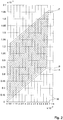
- Fig. 2 shows, in top plan view, the successive positions A,B,....Z of a line camera 3 with respect to a substrate 1 provided with a matrix structure M.
- the substrate 1 is provided with a pixel structure in which the pixels have dimensions of 50 * 150 micrometers.
- the line camera 3 having a length of approximately 1 mm includes an angle with the X-direction of approximately 49 degrees. This results in the line camera intersecting five pixel boundaries in Y-direction and intersecting thirteen pixel boundaries in X-direction.
- m and n are both prime numbers which are, in addition, mutually different, no or hardly any coinciding pulses for pixel boundaries in X-direction and pixel boundaries in Y-direction will occur, so that no or hardly any cross talk occurs in the signal. Therefore, per line camera position A,B,...Z, Fig. 2 shows no or hardly any positions on the line camera 3 which coincide with an intersection of pixel boundaries in X-direction and Y-direction. Both in X-direction and in Y-direction, the signals of the structural element boundaries are spatially separated well. It will be clear that the angle is different when the dimensions of the structural elements are different.
- a suitable angle which the main line of the line camera can include with the X-direction is 33.7 degrees. With that angle, with a line camera having a length of approximately 1 mm, three spatially separated pixel boundary intersections can be observed in X-direction and two spatially separated pixel boundary intersections can be observed in Y-direction. With unsuitably chosen angles, the spatial separation can decrease considerably (for instance with 0 and with 90 degrees) or a considerable cross talk can occur in the observation of the pixel boundaries in X-direction and the pixel boundaries in Y-direction. With square pixels, an angle of 45 degrees is, for instance, particularly unfavorable because of the large extent of cross talk in the signal.
- the relative X-position of the substrate structure with respect to the camera is derived from the m th result of the FFT processing of the camera signal and the relative Y-position of the substrate structure with respect to the camera is derived from the n th result of the FFT processing, with m being the number of pixel boundaries extending in Y-direction observed per line camera and with n being the number of pixel boundaries extending in X-direction observed per line camera.
- the amplitude of the m th result and the n th result is an indication of the reliability of the signal and the phase information of the m th result and the n th result is proportional to the relative X-position and the relative Y-position, respectively.
- the method and the apparatus may also be used for determining the position of a structure applied to a substrate, the substrate being intended for a different end product.
- options to be considered are electronics, memories, biomedical analysis arrays, TFT structures for LCD and placing components on a PC board.
- the structural elements on the substrate do not need to be pixel wells but may also be formed by other elements detectable with light, such as for instance electronic components in a chip, color filter elements and the like.
- the path of scanning over the substrate may be varied in many manners.
- scanning may also take place in an oblique direction, i.e. in a direction which includes an acute angle with the X-direction or the Y-direction.
- scanning may take place at a continuous speed and scanning may take place stepwise.
- a structure in the form of a printing may also have been applied to the substrate. The cameras then observe contrast differences instead of, for instance, height differences which are determined by the boundaries of the relief structural elements.
- the processing head instead of an inkjet printer head, the processing head may also comprise a lighting head, an ablation head or a processing head for placing components.
- the lighting may, for instance, take place with visible light, UV radiation, infrared radiation, X-ray or the like.
- the structural elements have dimensions larger than 300 micrometers, for obtaining a good accuracy and a reliable signal, the length of the main line along which the series of sensors of the camera are arranged needs to be increased.
- the structural elements are arranged in an orthogonal matrix.
- the relative position of a structure of which the structural elements are arranged in a non-orthogonal matrix can also be determined with the method and apparatus according to the invention.
- options to be considered are matrix structures with a round, trapezium or honeycomb structure.
Landscapes
- Engineering & Computer Science (AREA)
- Physics & Mathematics (AREA)
- General Physics & Mathematics (AREA)
- Automation & Control Theory (AREA)
- Human Computer Interaction (AREA)
- Manufacturing & Machinery (AREA)
- Length Measuring Devices By Optical Means (AREA)
- Electroluminescent Light Sources (AREA)
- Coating Apparatus (AREA)
- Application Of Or Painting With Fluid Materials (AREA)
- Testing Or Measuring Of Semiconductors Or The Like (AREA)
Description
- The invention relates to a method and an apparatus for determining the relative position of a processing head with respect to a substrate with a preformatted structure, with structural elements arranged in a matrix, wherein the matrix extends in an X-direction and Y-direction. The structure may be a relief structure but may also be a printing which provides a color difference structure on the substrate.
- Although the invention is not limited thereto, in order to give a better idea, this should particularly be understood to involve substrate dimensions of at least 10 mm * 10 mm, while the structural elements, such as for instance pixel wells of a substrate intended for manufacturing an OLED, have dimensions of the order of 20-500 micrometers, and while the distance between the structural elements is in the range of 2-40 micrometers. With regard to the accuracy with which the relative position of the substrate with respect to the processing head is to be provided, this should be understood to involve an accuracy which is of the order of 1 micrometer. For this, it likewise holds that the invention is not limited to such accuracies.
- Observing the position of a structure on a substrate is, for instance, carried out with the manufacture of displays, for instance OLEDs. For this, see for instance
EP-A-1 351 325 . With the manufacture of a display or another type of device, determining the position of, for instance, a relief structure is important for inter alia controlling a reading and/or writing laser or for controlling an inkjet printer head. A great accuracy is desired to have new structures fit to the existing structures as well as possible, so that the quality of the display or the other type of device is as high as possible. The problem with finding a position of a structure already present is that the accuracy of positioning sometimes leaves much to be desired. When the position of a structure already present on the substrate has not been determined accurately, a next layer on the substrate cannot be applied accurately. This results in a reduced quality of the display or other type of device and therefore in extra rejects in the production, which is unfavorable to the production costs. - The present invention contemplates a method with the aid of which the position of a structure on a substrate can be observed in a simple manner, while this is done very accurately, while the method for observation can be carried out quickly and inexpensively.
- To this end, the invention provides a method according to
claim 1. - The invention further provides an apparatus according to claim 19.
- With this method and apparatus, as a result of the fact that the main line of the camera includes an angle with the X-direction and with the Y-direction, a large number of structural element boundaries are located below the main line of the camera. These are structural element boundaries extending in X-direction as well as in Y-direction. The positions of the intersections of the structural element boundaries and the line camera are spatially separated over the length of the main line of the camera. In the further signal processing, all these spatially separated position information can be used for determining the relative X-position and the relative Y-position of the structure with respect to the camera. As a result, a very good signal-to-noise ratio (SNR) is obtained with the measurements and, in addition, a great accuracy is obtained with the position determination of the relative X-position and the relative Y-position.
- According to a further elaboration of the method and the apparatus, the angle of the main line with respect to the X-direction and the Y-direction is chosen or set such that m and n of the m spatially separated X-signals and n spatially separated Y-signals within the one-dimensional camera signal are mutually different prime numbers. Preferably, the signal-processing module of the apparatus is arranged for accurately deriving the relative X-position and Y-position of the at least one camera with respect to the substrate with the aid of signal processing comprising a fast Fourier transformation (FFT). Instead of a fast Fourier transformation, the signal processing may also comprise a discrete sine/cosine transformation. Here, the frequencies corresponding with the m spatially separated X-signals and the n spatially separated Y-signals will then be subjected to such a sine/cosine transformation in order to derive the relative X-position and Y-position with respect to the camera therefrom. In particular when m and n are mutually different prime numbers, there will be little cross talk in the signal between the X-position information-providing pulses and the Y-position information-providing pulses and therefore deriving the X-position information and the Y-position information can be done relatively simply and accurately.
- According to a further elaboration, a method and an apparatus are provided wherein the relative X-position of the substrate structure with respect to the camera is derivable from the mth result of the FFT processing of the camera signal and wherein the relative Y-position of the substrate structure with respect to the camera is derivable from the nth result of the FFT processing. Here, m is the number of spatially separated structural element boundaries extending in Y-direction which are simultaneously observed by the camera and n is the number of spatially separated structural element boundaries extending in X-direction which are simultaneously observed by the camera.
- Preferably, during a scanning pass, in which the relative X-position and Y-position are determined, further, an operation on the substrate is carried out with the processing head. This operation may, for instance, comprise an inkjet printer operation, a lighting, an ablation operation, and/or placing components on the substrate.
- According to a further elaboration of the invention, the X-position information, which is derived from the camera signal, is used for correcting the relative X-position of the processing head with respect to the substrate.
- According to a still further elaboration of the invention, the Y-position information, which is derived from the camera signal, is used for timing the operation, such as for instance timing the release of liquid by an inkjet printer head, the timing of the lighting by a lighting processing head, the timing of an ablation operation and/or the timing of the release of components.
- According to a further elaboration of the invention, the processing head is rotatable about a centerline extending at right angles to the substrate. It can thus be realized that the pitch in X-direction of, for instance, the nozzles of a processing head designed as an inkjet printer head is geared to the pitch of the substrate structure in X-direction.
- According to a still further elaboration of the invention, the at least one camera is preferably rotatable with respect to the processing head about a centerline extending at right angles to the substrate. Thus, the angle of the above-mentioned main line of the camera can be set such that the camera signal contains spatially separated X-position information and Y-position information.
- Preferably, the camera is a line camera. Such line cameras comprise a series of sensors arranged in line, for instance 1024 sensors together forming a line sensor. By using an objective for the line sensor, a desired part of the structure, for instance a linear part having a length of 1 mm, can be imaged on the line sensor.
- The invention will now be explained in more detail on the basis of an exemplary embodiment, with reference to the drawing, in which:
-
Fig. 1 shows an arrangement of an exemplary embodiment of an apparatus according to the invention; and -
Fig. 2 shows a top plan view of a substrate with the different successive camera positions shown therein. - The exemplary embodiment shown in
Fig. 1 shows asubstrate 1 which is supported by a substrate support which can displace thesubstrate 1 in X-direction and Y-direction. In the present exemplary embodiment, thesubstrate 1 is intended for manufacturing a display therefrom. On the substrate, an orthogonal matrix structure is present which is, in the present exemplary embodiment, a relief structure comprising pixel wells. The pixel wells have dimensions which are in the range of 20-500 micrometers. The distance between the edges of the pixel wells is in the range of 2-40 micrometers. Thesubstrate 1 has a length and a width of at least 10 mm * 10 mm but may also be much larger, for instance 1000 mm * 2000 mm. - The accuracy with which the X-position information and the Y-position information are to be provided is of the order of approximately 1 micrometer.
-
Fig. 1 also shows aprocessing head 2 which is provided with fourcameras 3, which are, in the present exemplary embodiment, designed as line cameras. The line cameras each comprise one series of sensors arranged along a main line. Each line camera observes, for instance, a length of approximately 1 mm and contains, for instance, 1024 sensors arranged next to one another along the main line. Such a line camera provides a one-dimensional signal which is subjected to signal processing. It is noted that two-dimensional CCD cameras may also be used, while, however, each time a one-dimensional signal of the CCD camera - i.e. a signal coming from a series of sensors arranged along one main line - will be subjected to signal processing. - In an alternative embodiment, the substrate may also be arranged statically and the
processing head 2 may be arranged movably in X-direction and Y-direction. In another alternative elaboration, thesubstrate 1 may, for instance, be arranged movably in Y-direction and theprocessing head 2 may, for instance, be arranged displacably in X-direction and vice versa. - The
processing head 2 is pivotal about a centerline extending at right angles to thesubstrate 1. Thecameras 3 are pivotal with respect to theprocessing head 2 about centerlines extending at right angles to the substrate. - Further, a
motion controller 4 is provided which controls the displacement of the substrate support. The Figure further shows a processing head driver 5 - in the present exemplary embodiment, the processing head is an inkjet printer head and theprocessing head driver 5 is an inkjetprinter head driver 5.Reference numeral 6 designates a signal-processing module. - The signal-
processing module 6 has the one-dimensional camera signals 7 coming from thecameras 3 as input information and also hasgeometrical knowledge 8 of the structure applied to thesubstrate 1. On the basis of fast Fourier transformation or discrete sine/cosine transformation of the one-dimensional camera signal of eachcamera 3, therelative displacement 9 of the X-position of thesubstrate 1 with respect to the expected position is determined. Thisdeviation 9 in X-direction may also be referred to by the term actual tracking deviation. Theactual tracking deviation 9 thus determined is used as an input signal for themotion controller 4. On the basis of fast Fourier transformation of the one-dimensional signal of eachcamera 3, the signal-processing module 6 also determines the relative displacement of the Y-position of the substrate with respect to the expected position. On the basis of this Y-position information, aprint trigger signal 10 is transmitted to themotion controller 4 by the signal-processing module 6. In the present exemplary embodiment, per pixel on thesubstrate 1, oneprint trigger 10 is transmitted to themotion controller 4. From themotion controller 4, a secondprint trigger signal 11 related to the clock is transmitted to the inkjetprinter head driver 5 which controls the different nozzles of theinkjet printer head 2. - In the present exemplary embodiment, the substrate length extends in Y-direction and the substrate width extends in X-direction. In a scanning pass, by a relative displacement of the
processing head 2 with thecameras 3 with respect to thesubstrate 1, the substrate is scanned in Y-direction over the whole substrate length. Then, a relative displacement of thesubstrate 1 with respect to theprocessing head 2 in X-direction is realized, after which a next scanning pass in Y-direction follows. The step of a scanning pass in Y-direction and a displacement in X-direction is repeated until thesubstrate 1 has been scanned over the whole substrate width. - The relative displacement in Y-direction may be either a stepwise displacement or a continuous displacement at a speed in the range of 0-40 m/s.
- The sampling frequency of the camera signal may be in the range of 1 kHz to 2 MHz.
- When there are structural elements having dimensions of the order of magnitude of about 150 micrometers and a scanning speed of approximately 0.4 m/s, a sampling frequency of 10 kHz is sufficient to prevent aliasing of signal pulses.
- The main line of the at least one camera includes an angle with the X-direction and includes an angle with the Y-direction. The above-mentioned angles deviate from 0 and from 90 degrees and have been chosen such that the camera signal contains spatially separated X-position information and Y-position information and that the X-position information and the Y-position information can be separated from the sensor signal with the aid of signal processing.
-
Fig. 2 shows, in top plan view, the successive positions A,B,....Z of aline camera 3 with respect to asubstrate 1 provided with a matrix structure M. In that exemplary embodiment, thesubstrate 1 is provided with a pixel structure in which the pixels have dimensions of 50 * 150 micrometers. Theline camera 3 having a length of approximately 1 mm includes an angle with the X-direction of approximately 49 degrees. This results in the line camera intersecting five pixel boundaries in Y-direction and intersecting thirteen pixel boundaries in X-direction. During scanning, each line camera provides m spatially separated X-signals and n spatially separated Y-signals, with m=13 and n=5. Due to the fact that, in the present exemplary embodiment, m and n are both prime numbers which are, in addition, mutually different, no or hardly any coinciding pulses for pixel boundaries in X-direction and pixel boundaries in Y-direction will occur, so that no or hardly any cross talk occurs in the signal. Therefore, per line camera position A,B,...Z,Fig. 2 shows no or hardly any positions on theline camera 3 which coincide with an intersection of pixel boundaries in X-direction and Y-direction. Both in X-direction and in Y-direction, the signals of the structural element boundaries are spatially separated well. It will be clear that the angle is different when the dimensions of the structural elements are different. When the pixels, for instance, have dimensions of 300 * 300 micrometers, a suitable angle which the main line of the line camera can include with the X-direction is 33.7 degrees. With that angle, with a line camera having a length of approximately 1 mm, three spatially separated pixel boundary intersections can be observed in X-direction and two spatially separated pixel boundary intersections can be observed in Y-direction. With unsuitably chosen angles, the spatial separation can decrease considerably (for instance with 0 and with 90 degrees) or a considerable cross talk can occur in the observation of the pixel boundaries in X-direction and the pixel boundaries in Y-direction. With square pixels, an angle of 45 degrees is, for instance, particularly unfavorable because of the large extent of cross talk in the signal. - During the signal processing in the signal-
processing module 6, the relative X-position of the substrate structure with respect to the camera is derived from the mth result of the FFT processing of the camera signal and the relative Y-position of the substrate structure with respect to the camera is derived from the nth result of the FFT processing, with m being the number of pixel boundaries extending in Y-direction observed per line camera and with n being the number of pixel boundaries extending in X-direction observed per line camera. - The amplitude of the mth result and the nth result is an indication of the reliability of the signal and the phase information of the mth result and the nth result is proportional to the relative X-position and the relative Y-position, respectively.
- Due to the fact that, with this method, of all structural element boundaries located below the main line of the camera, the information provided thereby is used, a very good signal-to-noise ratio (SNR) is obtained with the measurements and, in addition, a great accuracy is obtained in the position determination of the relative X-position and the relative Y-position.
- The invention is not limited to the exemplary embodiment described and, within the framework of the invention, as defined by the claims, various variants are possible. Thus, the method and the apparatus may also be used for determining the position of a structure applied to a substrate, the substrate being intended for a different end product. Here, options to be considered are electronics, memories, biomedical analysis arrays, TFT structures for LCD and placing components on a PC board. The structural elements on the substrate do not need to be pixel wells but may also be formed by other elements detectable with light, such as for instance electronic components in a chip, color filter elements and the like. Also, the path of scanning over the substrate may be varied in many manners. Instead of scanning in Y-direction and stepwise displacement in X-direction, scanning may also take place in an oblique direction, i.e. in a direction which includes an acute angle with the X-direction or the Y-direction. As already indicated, scanning may take place at a continuous speed and scanning may take place stepwise. Instead of a relief structure with pixel wells or similar structural elements, a structure in the form of a printing may also have been applied to the substrate. The cameras then observe contrast differences instead of, for instance, height differences which are determined by the boundaries of the relief structural elements. As already indicated hereinabove, instead of an inkjet printer head, the processing head may also comprise a lighting head, an ablation head or a processing head for placing components. The lighting may, for instance, take place with visible light, UV radiation, infrared radiation, X-ray or the like. When the structural elements have dimensions larger than 300 micrometers, for obtaining a good accuracy and a reliable signal, the length of the main line along which the series of sensors of the camera are arranged needs to be increased.
- In the exemplary embodiment described, the structural elements are arranged in an orthogonal matrix. However, the relative position of a structure of which the structural elements are arranged in a non-orthogonal matrix can also be determined with the method and apparatus according to the invention. Here, options to be considered are matrix structures with a round, trapezium or honeycomb structure.
Claims (27)
- A method including:- providing a substrate (1) with a preformatted structure with structural elements arranged in a matrix (M), wherein the matrix (M) extends in an X-direction and Y-direction;- providing a processing head (2)- providing at least one sensor which is connected with the processing head;- scanning the substrate with the at least one sensor;- providing at least one signal with the at least one sensor during the scanning;characterised in that:the at least one sensor comprises a camera (3) which comprises at least one series of sensors arranged along a main line that includes an angle with the X-direction and with the Y-direction, wherein the at least one signal that is provided by the camera (3) provides during the scanning at least one one-dimensional camera signal which, by virtue of the angle between the main line and the X-direction and the Y-direction, contains spatially separated X-position information embodied as m spatially separated X-signals, and wherein the camera signal, by virtue of the angle between the main line and the X-direction and the Y-direction, contains spatially separated Y-position information embodied as n spatially separated Y-signals,wherein the method additionally includes:- signal processing the camera signal to separate the X-position information and the Y-position information from the camera signal for real-time determining at least the X-position and the Y-position of the structure with respect to the camera (3).
- A method according to claim 12, wherein m and n are mutually different prime numbers.
- A method according to any one of the preceding claims, wherein the signal processing comprises a fast Fourier transformation (FFT).
- A method according to any one of claims 1-2, wherein the signal processing comprises a fast discrete sine/cosine transformation.
- A method according to claims 2 and 3, wherein the relative X-position of the substrate structure with respect to the camera (3) is derivable from the mth result of the FFT processing of the camera signal and wherein the relative Y-position of the substrate structure with respect to the camera (3) is derivable from the nth result of the FFT processing.
- A method according to any one of the preceding claims, wherein the substrate length extends in Y-direction and the substrate width extends in X-direction, wherein, in a scanning pass, by a relative displacement of the camera (3) with respect to the substrate (1), the substrate (1) is scanned in Y-direction over the whole substrate length, wherein then, a relative displacement of the substrate (1) with respect to the camera (3) in X-direction is realized, after which a next scanning pass in Y-direction follows.
- A method according to claim 6, wherein the step of a scanning pass in Y-direction and a displacement in X-direction are repeated until the substrate (1) has been scanned over the whole substrate width.
- A method according to any one of the preceding claims, wherein, during a scanning pass, further an operation on the substrate (1) is carried out with the processing head (2).
- A method according to any one of the preceding claims, wherein the operation is an inkjet printer operation.
- A method according to any one of the preceding claims, wherein the operation comprises a lighting.
- A method according to any one of the preceding claims, wherein the operation comprises an ablation operation.
- A method according to any one of the preceding claims, wherein the operation comprises placing components.
- A method according to any one of the preceding claims, wherein the speed of the relative displacement in Y-direction is either a stepwise displacement or a continuous displacement at a speed in the range of 0-40 m/s.
- A method according to any one of the preceding claims, wherein the sampling frequency of the camera signal is in the range of 1 kHz to 2 kHz.
- A method according to any one of the preceding claims, wherein the X-position information which is derived from the camera signal is used for correcting the relative X-position of the processing head (2) with respect to the substrate (1).
- A method according to any one of the preceding claims, wherein the Y-position information which is derived from the camera signal is used for timing the operation, such as for instance timing the release of liquid by an inkjet printer head, the timing of the lighting by a lighting processing head, the timing of an ablation operation and/or the timing of the release of components.
- A method according to any one of the preceding claims, wherein the substrate (1) which is provided has dimensions of at least 10 mm * 10 mm and wherein the structural elements have dimensions of the order of 20-50 micrometers, wherein the distance between the structural elements is in the range of 2-40 micrometers.
- A method according to any one of the preceding claims, wherein the accuracy with which the X-position information and the Y-position information are provided is of the order of 1 micrometer.
- An apparatus for carrying out an operation on a substrate (1), which substrate (1) is provided with a preformatted structure, with structural elements arranged in a matrix (M), wherein the matrix (M) extends in an X-direction and Y-direction, wherein the apparatus is provided with a substrate support and with a processing head (2), wherein a displacement mechanism is provided for relative displacement of the processing head (2) with respect to the substrate (1) wherein at least one sensor is connected with the processing head, wherein, in use, the at least one sensor is operatively displaced with respect to the substrate and thereby scans the substrate (1) for providing at least one signal, characterized in that, the at least one sensor comprises a camera (3) which comprises at least one series of sensors arranged along a main line that includes an angle with the X-direction and with the Y-direction, wherein the camera is configured for providing, during scanning, at least one one-dimensional camera signal which, by virtue of the angle between the main line and the X-direction and the Y-direction, contains spatially separated X-position information embodied as m spatially separated X-signals, and wherein the camera signal, by virtue of the angle between the main line and the X-direction and the Y direction, contains Y-position information embodied as n spatially separated Y-signals, , wherein the apparatus is provided with a control (4) which is provided with a signal-processing module (6) which is arranged for signal processing the camera signal to separate the X-position information and the Y-position information from the camera signal for real-time determining at least the X-position and the Y-position of the structure with respect to the camera (3).
- An apparatus according to claim 19, wherein m and n are mutually different prime numbers.
- An apparatus according to claim 19, wherein the signal-processing module (6) of the apparatus is arranged for carrying out a fast Fourier transformation (FFT).
- An apparatus according to claim 19, wherein the signal-processing module (6) of the apparatus is arranged for carrying out a fast discrete sine/cosine transformation.
- An apparatus according to claims 20 and 21, wherein the signal-processing module (6) is arranged for deriving the relative X-position of the substrate structure with respect to the camera (3) from the mth result of the FFT processing of the one-dimensional camera signal and for deriving the relative Y-position of the substrate structure with respect to the camera (3) from the nth result of the FFT processing of the one-dimensional camera signal.
- An apparatus according to any one of claims 19-23, wherein the processing head (2) is rotatable about a centerline extending at right angles to the substrate.
- An apparatus according to any one of claims 19 or 24, wherein the at least one camera (3) is rotatable with respect to the processing head (2) about a centerline extending at right angles to the substrate (1).
- An apparatus according to any one of claims 19-25, wherein the control (4) is arranged for using the X-position information which is derived from the camera signal for correcting the relative X-position of the processing head with respect to the substrate.
- An apparatus according to claims 19-26, wherein the control (4) is arranged for using the Y-position information which is derived from the camera signal for timing the operation, such as for instance timing the release of liquid by an inkjet printer head, the timing of the lighting by a lighting processing head, the timing of an ablation operation and/or the timing of the release of components.
Applications Claiming Priority (2)
| Application Number | Priority Date | Filing Date | Title |
|---|---|---|---|
| NL1030063A NL1030063C2 (en) | 2005-09-29 | 2005-09-29 | Method and device for determining a relative position of a processing head relative to a substrate with a structure. |
| PCT/NL2006/000487 WO2007037683A2 (en) | 2005-09-29 | 2006-09-29 | Method and apparatus for determining a relative position of a processing head with respect to a substrate with a structure |
Publications (2)
| Publication Number | Publication Date |
|---|---|
| EP1946192A2 EP1946192A2 (en) | 2008-07-23 |
| EP1946192B1 true EP1946192B1 (en) | 2016-12-28 |
Family
ID=36480881
Family Applications (1)
| Application Number | Title | Priority Date | Filing Date |
|---|---|---|---|
| EP06799476.4A Not-in-force EP1946192B1 (en) | 2005-09-29 | 2006-09-29 | Method and apparatus for determining a relative position of a processing head with respect to a substrate with a structure |
Country Status (8)
| Country | Link |
|---|---|
| US (1) | US7692174B2 (en) |
| EP (1) | EP1946192B1 (en) |
| JP (1) | JP2009509746A (en) |
| KR (1) | KR101345251B1 (en) |
| CN (1) | CN101258452B (en) |
| NL (1) | NL1030063C2 (en) |
| TW (1) | TWI348236B (en) |
| WO (1) | WO2007037683A2 (en) |
Family Cites Families (5)
| Publication number | Priority date | Publication date | Assignee | Title |
|---|---|---|---|---|
| US5867590A (en) * | 1995-01-11 | 1999-02-02 | Nova Measuring Instruments, Ltd. | Method and apparatus for determining a location on a surface of an object |
| US5803635A (en) * | 1995-05-04 | 1998-09-08 | Intermec Corporation | Method and apparatus to determine position and sense motion of linerless media |
| JP3366497B2 (en) * | 1995-07-12 | 2003-01-14 | 松下電器産業株式会社 | Component detection method |
| DE19840301A1 (en) * | 1998-09-04 | 2000-03-09 | Colorpartner Gmbh Entwicklung | Printing graphical illustrations on both sides of base material with digital triggering of two individual printing units on smooth printing material like paper or plastics film |
| NL1020312C2 (en) * | 2002-04-05 | 2003-10-07 | Otb Groep B V | Method and device for manufacturing a display, such as for example a polymeric OLED display, a display and a substrate for use in the method. |
-
2005
- 2005-09-29 NL NL1030063A patent/NL1030063C2/en not_active IP Right Cessation
-
2006
- 2006-09-29 WO PCT/NL2006/000487 patent/WO2007037683A2/en not_active Ceased
- 2006-09-29 TW TW095136416A patent/TWI348236B/en active
- 2006-09-29 JP JP2008533275A patent/JP2009509746A/en active Pending
- 2006-09-29 EP EP06799476.4A patent/EP1946192B1/en not_active Not-in-force
- 2006-09-29 US US11/990,088 patent/US7692174B2/en not_active Expired - Fee Related
- 2006-09-29 CN CN2006800323336A patent/CN101258452B/en not_active Expired - Fee Related
-
2008
- 2008-03-26 KR KR1020087007316A patent/KR101345251B1/en not_active Expired - Fee Related
Non-Patent Citations (1)
| Title |
|---|
| None * |
Also Published As
| Publication number | Publication date |
|---|---|
| WO2007037683A3 (en) | 2007-06-28 |
| TW200731590A (en) | 2007-08-16 |
| JP2009509746A (en) | 2009-03-12 |
| CN101258452A (en) | 2008-09-03 |
| US20090134347A1 (en) | 2009-05-28 |
| TWI348236B (en) | 2011-09-01 |
| KR101345251B1 (en) | 2013-12-26 |
| WO2007037683A2 (en) | 2007-04-05 |
| KR20080056169A (en) | 2008-06-20 |
| NL1030063C2 (en) | 2007-03-30 |
| EP1946192A2 (en) | 2008-07-23 |
| CN101258452B (en) | 2011-05-18 |
| US7692174B2 (en) | 2010-04-06 |
Similar Documents
| Publication | Publication Date | Title |
|---|---|---|
| US20070070109A1 (en) | Methods and systems for calibration of inkjet drop positioning | |
| US20060158474A1 (en) | Method and device for accurately positioning a pattern on a substrate | |
| US20240173961A1 (en) | Ejection control using substrate alignment features and print region alignment features | |
| JP6805028B2 (en) | Droplet ejection device, droplet ejection method, program and computer storage medium | |
| US9749621B2 (en) | Calibration plate for calibrating a plurality of image capturing devices and method for calibrating a plurality of image capturing devices | |
| US9102168B2 (en) | Method for applying a marking on an object and marking apparatus | |
| EP2324932A1 (en) | Inkjet image-drawing device | |
| JP2008544333A (en) | Inkjet printing system and method for flat panel display | |
| CN101584035A (en) | Substrate processing apparatus and substrate processing method | |
| KR20210108890A (en) | Inkjet printing method and inkjet printing apparatus | |
| US7692174B2 (en) | Method and apparatus for determining a relative position of a processing head with respect to a substrate with a structure | |
| US9880089B2 (en) | High-density devices with synchronous tracks for quad-cell based alignment correction | |
| US7224474B2 (en) | Positioning method for biochip | |
| EP2058135A1 (en) | Printer device and method for producing biological test arrays | |
| JP2006130383A (en) | Dot shift detection method and dot shift detection device | |
| JP2006245174A (en) | Positioning stage, pattern forming device, inspection device, position correction method, substrate support part | |
| HK1115649A (en) | Method and apparatus for determining a relative position of a processing head with respect to a substrate with a structure | |
| US9009957B2 (en) | Method for placing a component on a substrate | |
| KR101261353B1 (en) | Plotting point data acquisition method and device, plotting method and device | |
| JP2004151083A (en) | Image alignment apparatus for biochip manufacturing device and image alignment method for the manufacturing device | |
| US20260021504A1 (en) | Coating device and method of driving the same | |
| JP2011069997A (en) | Alignment apparatus | |
| JP5873712B2 (en) | Coating device | |
| JP2013120108A (en) | Thin film formation device and thin film formation method | |
| MX2008003466A (en) | Device for determining the relative position of two substantially flat elements |
Legal Events
| Date | Code | Title | Description |
|---|---|---|---|
| PUAI | Public reference made under article 153(3) epc to a published international application that has entered the european phase |
Free format text: ORIGINAL CODE: 0009012 |
|
| 17P | Request for examination filed |
Effective date: 20080423 |
|
| AK | Designated contracting states |
Kind code of ref document: A2 Designated state(s): AT BE BG CH CY CZ DE DK EE ES FI FR GB GR HU IE IS IT LI LT LU LV MC NL PL PT RO SE SI SK TR |
|
| RAP1 | Party data changed (applicant data changed or rights of an application transferred) |
Owner name: OTB SOLAR B.V. |
|
| DAX | Request for extension of the european patent (deleted) | ||
| RAP1 | Party data changed (applicant data changed or rights of an application transferred) |
Owner name: ROTH & RAU B.V. |
|
| 17Q | First examination report despatched |
Effective date: 20150309 |
|
| GRAP | Despatch of communication of intention to grant a patent |
Free format text: ORIGINAL CODE: EPIDOSNIGR1 |
|
| INTG | Intention to grant announced |
Effective date: 20160922 |
|
| GRAS | Grant fee paid |
Free format text: ORIGINAL CODE: EPIDOSNIGR3 |
|
| GRAA | (expected) grant |
Free format text: ORIGINAL CODE: 0009210 |
|
| RAP1 | Party data changed (applicant data changed or rights of an application transferred) |
Owner name: MEYER BURGER (NETHERLANDS) B.V. |
|
| AK | Designated contracting states |
Kind code of ref document: B1 Designated state(s): AT BE BG CH CY CZ DE DK EE ES FI FR GB GR HU IE IS IT LI LT LU LV MC NL PL PT RO SE SI SK TR |
|
| REG | Reference to a national code |
Ref country code: GB Ref legal event code: FG4D |
|
| REG | Reference to a national code |
Ref country code: CH Ref legal event code: EP |
|
| REG | Reference to a national code |
Ref country code: AT Ref legal event code: REF Ref document number: 857825 Country of ref document: AT Kind code of ref document: T Effective date: 20170115 |
|
| REG | Reference to a national code |
Ref country code: IE Ref legal event code: FG4D |
|
| REG | Reference to a national code |
Ref country code: DE Ref legal event code: R096 Ref document number: 602006051385 Country of ref document: DE |
|
| PG25 | Lapsed in a contracting state [announced via postgrant information from national office to epo] |
Ref country code: LV Free format text: LAPSE BECAUSE OF FAILURE TO SUBMIT A TRANSLATION OF THE DESCRIPTION OR TO PAY THE FEE WITHIN THE PRESCRIBED TIME-LIMIT Effective date: 20161228 |
|
| REG | Reference to a national code |
Ref country code: NL Ref legal event code: FP |
|
| REG | Reference to a national code |
Ref country code: LT Ref legal event code: MG4D |
|
| PG25 | Lapsed in a contracting state [announced via postgrant information from national office to epo] |
Ref country code: SE Free format text: LAPSE BECAUSE OF FAILURE TO SUBMIT A TRANSLATION OF THE DESCRIPTION OR TO PAY THE FEE WITHIN THE PRESCRIBED TIME-LIMIT Effective date: 20161228 Ref country code: GR Free format text: LAPSE BECAUSE OF FAILURE TO SUBMIT A TRANSLATION OF THE DESCRIPTION OR TO PAY THE FEE WITHIN THE PRESCRIBED TIME-LIMIT Effective date: 20170329 Ref country code: LT Free format text: LAPSE BECAUSE OF FAILURE TO SUBMIT A TRANSLATION OF THE DESCRIPTION OR TO PAY THE FEE WITHIN THE PRESCRIBED TIME-LIMIT Effective date: 20161228 |
|
| REG | Reference to a national code |
Ref country code: AT Ref legal event code: MK05 Ref document number: 857825 Country of ref document: AT Kind code of ref document: T Effective date: 20161228 |
|
| PG25 | Lapsed in a contracting state [announced via postgrant information from national office to epo] |
Ref country code: FI Free format text: LAPSE BECAUSE OF FAILURE TO SUBMIT A TRANSLATION OF THE DESCRIPTION OR TO PAY THE FEE WITHIN THE PRESCRIBED TIME-LIMIT Effective date: 20161228 |
|
| PG25 | Lapsed in a contracting state [announced via postgrant information from national office to epo] |
Ref country code: CZ Free format text: LAPSE BECAUSE OF FAILURE TO SUBMIT A TRANSLATION OF THE DESCRIPTION OR TO PAY THE FEE WITHIN THE PRESCRIBED TIME-LIMIT Effective date: 20161228 Ref country code: RO Free format text: LAPSE BECAUSE OF FAILURE TO SUBMIT A TRANSLATION OF THE DESCRIPTION OR TO PAY THE FEE WITHIN THE PRESCRIBED TIME-LIMIT Effective date: 20161228 Ref country code: IS Free format text: LAPSE BECAUSE OF FAILURE TO SUBMIT A TRANSLATION OF THE DESCRIPTION OR TO PAY THE FEE WITHIN THE PRESCRIBED TIME-LIMIT Effective date: 20170428 Ref country code: SK Free format text: LAPSE BECAUSE OF FAILURE TO SUBMIT A TRANSLATION OF THE DESCRIPTION OR TO PAY THE FEE WITHIN THE PRESCRIBED TIME-LIMIT Effective date: 20161228 Ref country code: EE Free format text: LAPSE BECAUSE OF FAILURE TO SUBMIT A TRANSLATION OF THE DESCRIPTION OR TO PAY THE FEE WITHIN THE PRESCRIBED TIME-LIMIT Effective date: 20161228 |
|
| PG25 | Lapsed in a contracting state [announced via postgrant information from national office to epo] |
Ref country code: BG Free format text: LAPSE BECAUSE OF FAILURE TO SUBMIT A TRANSLATION OF THE DESCRIPTION OR TO PAY THE FEE WITHIN THE PRESCRIBED TIME-LIMIT Effective date: 20170328 Ref country code: PL Free format text: LAPSE BECAUSE OF FAILURE TO SUBMIT A TRANSLATION OF THE DESCRIPTION OR TO PAY THE FEE WITHIN THE PRESCRIBED TIME-LIMIT Effective date: 20161228 Ref country code: AT Free format text: LAPSE BECAUSE OF FAILURE TO SUBMIT A TRANSLATION OF THE DESCRIPTION OR TO PAY THE FEE WITHIN THE PRESCRIBED TIME-LIMIT Effective date: 20161228 Ref country code: BE Free format text: LAPSE BECAUSE OF FAILURE TO SUBMIT A TRANSLATION OF THE DESCRIPTION OR TO PAY THE FEE WITHIN THE PRESCRIBED TIME-LIMIT Effective date: 20161228 Ref country code: ES Free format text: LAPSE BECAUSE OF FAILURE TO SUBMIT A TRANSLATION OF THE DESCRIPTION OR TO PAY THE FEE WITHIN THE PRESCRIBED TIME-LIMIT Effective date: 20161228 Ref country code: IT Free format text: LAPSE BECAUSE OF FAILURE TO SUBMIT A TRANSLATION OF THE DESCRIPTION OR TO PAY THE FEE WITHIN THE PRESCRIBED TIME-LIMIT Effective date: 20161228 Ref country code: PT Free format text: LAPSE BECAUSE OF FAILURE TO SUBMIT A TRANSLATION OF THE DESCRIPTION OR TO PAY THE FEE WITHIN THE PRESCRIBED TIME-LIMIT Effective date: 20170428 |
|
| REG | Reference to a national code |
Ref country code: DE Ref legal event code: R097 Ref document number: 602006051385 Country of ref document: DE |
|
| PLBE | No opposition filed within time limit |
Free format text: ORIGINAL CODE: 0009261 |
|
| STAA | Information on the status of an ep patent application or granted ep patent |
Free format text: STATUS: NO OPPOSITION FILED WITHIN TIME LIMIT |
|
| PG25 | Lapsed in a contracting state [announced via postgrant information from national office to epo] |
Ref country code: DK Free format text: LAPSE BECAUSE OF FAILURE TO SUBMIT A TRANSLATION OF THE DESCRIPTION OR TO PAY THE FEE WITHIN THE PRESCRIBED TIME-LIMIT Effective date: 20161228 |
|
| 26N | No opposition filed |
Effective date: 20170929 |
|
| PG25 | Lapsed in a contracting state [announced via postgrant information from national office to epo] |
Ref country code: SI Free format text: LAPSE BECAUSE OF FAILURE TO SUBMIT A TRANSLATION OF THE DESCRIPTION OR TO PAY THE FEE WITHIN THE PRESCRIBED TIME-LIMIT Effective date: 20161228 |
|
| REG | Reference to a national code |
Ref country code: CH Ref legal event code: PL |
|
| PG25 | Lapsed in a contracting state [announced via postgrant information from national office to epo] |
Ref country code: MC Free format text: LAPSE BECAUSE OF FAILURE TO SUBMIT A TRANSLATION OF THE DESCRIPTION OR TO PAY THE FEE WITHIN THE PRESCRIBED TIME-LIMIT Effective date: 20161228 |
|
| REG | Reference to a national code |
Ref country code: IE Ref legal event code: MM4A |
|
| PG25 | Lapsed in a contracting state [announced via postgrant information from national office to epo] |
Ref country code: LU Free format text: LAPSE BECAUSE OF NON-PAYMENT OF DUE FEES Effective date: 20170929 |
|
| REG | Reference to a national code |
Ref country code: FR Ref legal event code: ST Effective date: 20180531 |
|
| PG25 | Lapsed in a contracting state [announced via postgrant information from national office to epo] |
Ref country code: IE Free format text: LAPSE BECAUSE OF NON-PAYMENT OF DUE FEES Effective date: 20170929 Ref country code: CH Free format text: LAPSE BECAUSE OF NON-PAYMENT OF DUE FEES Effective date: 20170930 Ref country code: LI Free format text: LAPSE BECAUSE OF NON-PAYMENT OF DUE FEES Effective date: 20170930 |
|
| PG25 | Lapsed in a contracting state [announced via postgrant information from national office to epo] |
Ref country code: FR Free format text: LAPSE BECAUSE OF NON-PAYMENT OF DUE FEES Effective date: 20171002 |
|
| PG25 | Lapsed in a contracting state [announced via postgrant information from national office to epo] |
Ref country code: HU Free format text: LAPSE BECAUSE OF FAILURE TO SUBMIT A TRANSLATION OF THE DESCRIPTION OR TO PAY THE FEE WITHIN THE PRESCRIBED TIME-LIMIT; INVALID AB INITIO Effective date: 20060929 |
|
| PG25 | Lapsed in a contracting state [announced via postgrant information from national office to epo] |
Ref country code: CY Free format text: LAPSE BECAUSE OF NON-PAYMENT OF DUE FEES Effective date: 20161228 |
|
| PG25 | Lapsed in a contracting state [announced via postgrant information from national office to epo] |
Ref country code: TR Free format text: LAPSE BECAUSE OF FAILURE TO SUBMIT A TRANSLATION OF THE DESCRIPTION OR TO PAY THE FEE WITHIN THE PRESCRIBED TIME-LIMIT Effective date: 20161228 |
|
| REG | Reference to a national code |
Ref country code: DE Ref legal event code: R081 Ref document number: 602006051385 Country of ref document: DE Owner name: SUSS MICROTEC LITHOGRAPHY GMBH, DE Free format text: FORMER OWNER: MEYER BURGER (NETHERLANDS) B.V., EINDHOVEN, NL |
|
| PGFP | Annual fee paid to national office [announced via postgrant information from national office to epo] |
Ref country code: DE Payment date: 20200928 Year of fee payment: 15 Ref country code: GB Payment date: 20200922 Year of fee payment: 15 Ref country code: NL Payment date: 20200925 Year of fee payment: 15 |
|
| REG | Reference to a national code |
Ref country code: DE Ref legal event code: R119 Ref document number: 602006051385 Country of ref document: DE |
|
| REG | Reference to a national code |
Ref country code: NL Ref legal event code: MM Effective date: 20211001 |
|
| GBPC | Gb: european patent ceased through non-payment of renewal fee |
Effective date: 20210929 |
|
| PG25 | Lapsed in a contracting state [announced via postgrant information from national office to epo] |
Ref country code: NL Free format text: LAPSE BECAUSE OF NON-PAYMENT OF DUE FEES Effective date: 20211001 |
|
| PG25 | Lapsed in a contracting state [announced via postgrant information from national office to epo] |
Ref country code: GB Free format text: LAPSE BECAUSE OF NON-PAYMENT OF DUE FEES Effective date: 20210929 Ref country code: DE Free format text: LAPSE BECAUSE OF NON-PAYMENT OF DUE FEES Effective date: 20220401 |