EP1942663A1 - Column current source - Google Patents
Column current source Download PDFInfo
- Publication number
- EP1942663A1 EP1942663A1 EP07100006A EP07100006A EP1942663A1 EP 1942663 A1 EP1942663 A1 EP 1942663A1 EP 07100006 A EP07100006 A EP 07100006A EP 07100006 A EP07100006 A EP 07100006A EP 1942663 A1 EP1942663 A1 EP 1942663A1
- Authority
- EP
- European Patent Office
- Prior art keywords
- current
- image sensor
- resistor means
- current source
- column
- Prior art date
- Legal status (The legal status is an assumption and is not a legal conclusion. Google has not performed a legal analysis and makes no representation as to the accuracy of the status listed.)
- Granted
Links
Images


Classifications
-
- H—ELECTRICITY
- H04—ELECTRIC COMMUNICATION TECHNIQUE
- H04N—PICTORIAL COMMUNICATION, e.g. TELEVISION
- H04N23/00—Cameras or camera modules comprising electronic image sensors; Control thereof
- H04N23/60—Control of cameras or camera modules
- H04N23/65—Control of camera operation in relation to power supply
- H04N23/651—Control of camera operation in relation to power supply for reducing power consumption by affecting camera operations, e.g. sleep mode, hibernation mode or power off of selective parts of the camera
-
- H—ELECTRICITY
- H04—ELECTRIC COMMUNICATION TECHNIQUE
- H04N—PICTORIAL COMMUNICATION, e.g. TELEVISION
- H04N25/00—Circuitry of solid-state image sensors [SSIS]; Control thereof
-
- H—ELECTRICITY
- H04—ELECTRIC COMMUNICATION TECHNIQUE
- H04N—PICTORIAL COMMUNICATION, e.g. TELEVISION
- H04N25/00—Circuitry of solid-state image sensors [SSIS]; Control thereof
- H04N25/70—SSIS architectures; Circuits associated therewith
- H04N25/76—Addressed sensors, e.g. MOS or CMOS sensors
- H04N25/78—Readout circuits for addressed sensors, e.g. output amplifiers or A/D converters
Definitions
- the present invention relates to a column current source for an image sensor and in particular, but not exclusively, for minimising the current usage of a column current source for an image sensor.
- Image sensors traditionally are made up of an array of light sensitive pixels. The image sensor requires to read-out the value of each pixel to produce an image. Before the array of pixels is exposed to receive light, each pixel must be reset.
- a current column source ICOL is provided for each column to bias the pixels PIX of that column and, as such, reset their values.
- Each column current source ICOL is one half of a current mirror circuit.
- a diode connected transistor MBIAS makes up the other half of the current mirror and is common to each column current source ICOL.
- the current ICOLBIAS is mirrored at ICOL ⁇ 1> to ICOL ⁇ col>.
- the current column source ICOL is not required continuously during an imaging cycle but only when the pixel values require to be reset for integration and readout.
- the circuit comprises two reference currents in parallel I1 and I2.
- a switch SW is provided for selectively connecting the reference current I2. When the current sources are required the switch is closed and ICOLBIAS is equal to I1 + I2. When the current sources are not required, the switch SW is opened and ICOLBIAS is equal to 11.
- a single current source is used in combination with a resistive load to provide two levels of reference current depending on whether the resistive load is short-circuited or not.
- a plurality of column current sources 10 are shown.
- Each column current source 10 has common elements being a diode connected transistor MBIAS and reference current source ICOLBIAS thereby forming a current mirror.
- a series of resistors MRESLOAD are connected between each current column source 10 and the transistor MBIAS.
- a switch 12 is connected across the series of resistors MRESLOAD enabling a short across the series of resistors MRESLOAD.
- the switch 12 When the column current sources 10 are required the switch 12 is turned on shorting the series of resistors MRESLOAD and allowing the currents ICOL ⁇ 1> to ICOL ⁇ 4> to "mirror" ICOLBIAS.
- the switch 12 When the column current sources 10 are not required the switch 12 is turned off.
- the series of resistors MRESLOAD now have a potential difference across them which reduces the gate-source voltage of the transistor MBIAS.
- the column current sources 10 and transistor MBIAS form a current mirror, the column current sources 10 mirror the gate-source voltage of MBIAS and therefore the currents ICOL ⁇ 1> to ICOL ⁇ 4> are reduced accordingly.
- the column current sources are either at a low value or a high value depending on whether the pixel and associated circuitry is in operation or not.
- a high value of current is only required when the transfer gate transistor has been switched on.
- an image sensor comprising:
- the source of the transistor is connected to the reference current source
- the gate of the transistor is also connected to the reference current source as well as each of the plurality of current sources.
- the plurality of current sources are column transistors.
- the resistor means is a NMOS transistor operating in its linear region.
- the further resistor means is a NMOS transistor operating in its linear region.
- the resistor means comprises a resistive element for each column.
- the resistor means is a single resistive element.
- the or each further resistor means comprises a plurality of resistive elements.
- the or each further resistor means is a single resistive element.
- the size of the circuit can be reduced by only using one resistive element common to each column current source.
- a resistive element may comprise a NMOS transistor in its linear region. It is also possible to use a resistive element for each column of the array of pixels.
- a mobile device comprising an image sensor according to a first aspect of the present invention.
- the mobile device is a mobile phone having a camera including the image sensor
- an optical pointing device comprising an image sensor according to a first aspect of the present invention.
- the optical pointing device is an optical mouse.
- a pixel 20 is shown having a photodiode PD, a reset transistor RST, a transfer gate transistor TG, a read transistor RD and a pixel buffer transistor (MBUF), which acts as a source follower.
- the pixel 20 is part of a pixel array (not shown) and resides in a column of pixels of the pixel array connected in a similar manner between a voltage supply VRT and a column current source IV X .
- Each column has an associated parasitic capacitance C parasitic and a readout circuit 22.
- the readout circuit 22 comprises a correlated double sample (CDS) arrangement having a signal sample capacitor CSIG, a reset sample capacitor CBLK, a CDS signal transistor CDSSIG, a CDS reset transistor CDSBLK, a comparator COMP.
- CDS correlated double sample
- a pixel array having columns of pixels PIX is shown. Only one pixel is shown in each column but it should be appreciated that, as the diagram is for explanation purposes, that there could be more than one pixel in the column.
- Each column has a column current source ICOL ⁇ n> (ICOL ⁇ n> representing ICOL ⁇ 1> to ICOL ⁇ 8>), which is represented by a transistor and is equivalent to the column current source IV X of Fig. 3 .
- Each column current source ICOL ⁇ n> has common elements being a diode connected transistor MBIAS and reference current source ICOLBIAS thereby forming a current mirror.
- a first set of resistors MRESLOAD1 are connected in parallel between a first common node SGND1, which, in this example, is equivalent to ground and is also common to the column current sources ICOL ⁇ n>, and a second common node SGND2.
- a second set of resistors MRESLOAD2 is connected in parallel between the second common node and the diode connected transistor MBIAS, although, in this example, a resistor R is connected between transistor MBIAS and the second set of resistors MRESLOAD2. Although resistor R is not necessary, having it present helps the matching of bias and current sources.
- the sets of resistors MRESLOAD1 and MRESLOAD2 may be a single resistive element or a number of resistive elements.
- the resistive elements are NMOS transistors operating in their linear region to emulate a resistor.
- a first switch HICURANA1 is connected between the first common node SGND1 and the transistor MBIAS and a second switch HICURANA2 is connected between the second common node SGND2 and the transistor MBIAS. Turning HICURANA1 on thereby short circuits the first set of resistors MRESLOAD1 and turning HICURANA2 on short circuits the second set of resistors MRESLOAD2.
- the first switch HICURANA1 When the column current sources ICOL ⁇ n> are required at the highest current level the first switch HICURANA1 is turned on shorting the first and second sets of resistors MRESLOAD1, MRESLOAD2 and allowing the currents ICOL ⁇ n> to "mirror" ICOLBIAS.
- the first switch HICURANA1 When the column current sources ICOL ⁇ n> are required at a medium level, the first switch HICURANA1 is turned off and the second switch HICURANA2 is turned on.
- the first set of resistors MRESLOAD1 now have a potential difference across them which reduces the gate-source voltage of the transistor MBIAS.
- the column current sources ICOL ⁇ n> and transistor MBIAS form a current mirror, the column current sources ICOL ⁇ n> mirror the gate-source voltage of MBIAS and therefore the currents available at ICOL ⁇ n> are reduced accordingly.
- the resistance of the first set of resistors MRESLOAD1 is chosen to only reduce the currents available at ICOL ⁇ n> by a pre-determined amount.
- the first and second switches HICURANA1, HICURANA2 are turned off.
- the first set of resistors MRESLOAD1 and the second set of resistors now have a potential difference across them which reduces the gate-source voltage of the transistor MBIAS even further.
- the column current sources ICOL ⁇ n> and transistor MBIAS form a current mirror, the column current sources ICOL ⁇ n> mirror the gate-source voltage of MBIAS and therefore the currents available at ICOL ⁇ n> are reduced accordingly.
- the resistance of the second set of resistors MRESLOAD2 is chosen to reduce the currents available at ICOL ⁇ n> to as low as possible.
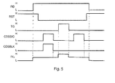
- the effect of the above circuit arrangements will now be described in relation to a timing diagram shown in Fig. 5 .
- the first five signals RD, RST, TG, CDSSIG and CDSBLK represent the on/off operation of the transistors which have like references in Fig. 3 .
- the sixth signal IV X represents the current level available at the current source IV X of Fig. 3 , which is equivalent to the column current sources ICOL ⁇ n> of Fig. 4 .
- transistor RD is turned on, represented by signal RD going high.
- transistor RST is turned off, represented by signal RST going low.
- a value representing the reset state of the pixel is then sampled onto the reset sample capacitor CBLK by pulsing transistors CDSSIG and CDSBLK, which corresponds to the first sample of a CDS process.
- Information from the photodiode PD is then transferred to node FDN by pulsing transistor TG.
- the signal at FDN is then sampled onto the signal sample capacitor CSIG by pulsing CDSSIG, which corresponds to the second sample of the CDS process.
- transistor RST is turned off followed by transistor RD completing the readout sequence.
- the pixel buffer MBUF is a source follower and can therefore source current easily but its ability to sink current is limited by the column current source. As such, the current required from the column source is dependent on ensuring that pixel buffer MBUF has settled after a switching operation.
- the sets of resistors MRESLOAD1 and MRESLOAD2 may be replaced with a single resistance. This allows the footprint of the circuit to be reduced when applied in silicon.
- the present invention allows the current consumption of a pixel array in an image sensor to be reduced. This is particularly relevant where the image sensor is used in mobile applications, such as a cellular telephone.
Landscapes
- Engineering & Computer Science (AREA)
- Multimedia (AREA)
- Signal Processing (AREA)
- Transforming Light Signals Into Electric Signals (AREA)
Abstract
Description
- The present invention relates to a column current source for an image sensor and in particular, but not exclusively, for minimising the current usage of a column current source for an image sensor.
- Image sensors traditionally are made up of an array of light sensitive pixels. The image sensor requires to read-out the value of each pixel to produce an image. Before the array of pixels is exposed to receive light, each pixel must be reset.
- As shown in prior art
Fig. 1 , a current column source ICOL is provided for each column to bias the pixels PIX of that column and, as such, reset their values. - Each column current source ICOL is one half of a current mirror circuit. A diode connected transistor MBIAS makes up the other half of the current mirror and is common to each column current source ICOL.
- The current ICOLBIAS is mirrored at ICOL<1> to ICOL<col>.
- The current column source ICOL is not required continuously during an imaging cycle but only when the pixel values require to be reset for integration and readout.
- Consequently, to reduce power consumption the circuit comprises two reference currents in parallel I1 and I2. A switch SW is provided for selectively connecting the reference current I2. When the current sources are required the switch is closed and ICOLBIAS is equal to I1 + I2. When the current sources are not required, the switch SW is opened and ICOLBIAS is equal to 11.
- When switching between values of ICOLBIAS there is an inherent lag associated with powering up and down of the array due to the associated parasitic capacitance of the array. It may take 5ms or longer to switch between values of ICOLBIAS. As pixel arrays get larger the parasitic capacitance increases and the time to switch between values of ICOLBIAS increases further.
- As such, as shown in prior art
Fig. 2 , which relates toEuropean Patent Application 04252834.9 Fig. 2 a plurality of columncurrent sources 10 are shown. Each columncurrent source 10 has common elements being a diode connected transistor MBIAS and reference current source ICOLBIAS thereby forming a current mirror. A series of resistors MRESLOAD are connected between eachcurrent column source 10 and the transistor MBIAS. Aswitch 12 is connected across the series of resistors MRESLOAD enabling a short across the series of resistors MRESLOAD. - When the column
current sources 10 are required theswitch 12 is turned on shorting the series of resistors MRESLOAD and allowing the currents ICOL<1> to ICOL<4> to "mirror" ICOLBIAS. - When the column
current sources 10 are not required theswitch 12 is turned off. The series of resistors MRESLOAD now have a potential difference across them which reduces the gate-source voltage of the transistor MBIAS. As the columncurrent sources 10 and transistor MBIAS form a current mirror, the columncurrent sources 10 mirror the gate-source voltage of MBIAS and therefore the currents ICOL<1> to ICOL<4> are reduced accordingly. - With both of the above arrangements the column current sources are either at a low value or a high value depending on whether the pixel and associated circuitry is in operation or not. In fact, for a 4T pixel, a high value of current is only required when the transfer gate transistor has been switched on. At other times, it would be possible to use a medium value current level, which would result in less current being consumed during pixel readout.
- According to a first aspect of the present invention there is provided an image sensor comprising:
- an array of pixels arranged in rows and columns;
- a reference current source;
- a transistor connected as a source follower to the reference current source and forming one half of a current mirror;
- a plurality of current sources each connected to a column of pixels and each current source forming the other half of the current mirror and thereby mirroring the reference current source, wherein the current sources are connected to a first common node,
- It is traditional to refer to a "column" current source in an image sensor but it should be appreciated that the orientation of the image sensor could be rotated without affecting the principal of the invention.
- Preferably, there is one further resistor means and two switch means enabling three different levels to be supplied by the plurality of current sources.
- Preferably, the source of the transistor is connected to the reference current source, the gate of the transistor is also connected to the reference current source as well as each of the plurality of current sources.
- Preferably, the plurality of current sources are column transistors.
- Preferably, the resistor means is a NMOS transistor operating in its linear region.
- Preferably, the further resistor means is a NMOS transistor operating in its linear region.
- Preferably, the resistor means comprises a resistive element for each column.
- Alternatively, the resistor means is a single resistive element.
- Preferably, the or each further resistor means comprises a plurality of resistive elements.
- Alternatively, the or each further resistor means is a single resistive element.
- The size of the circuit can be reduced by only using one resistive element common to each column current source. For example, a resistive element may comprise a NMOS transistor in its linear region. It is also possible to use a resistive element for each column of the array of pixels.
- According to a second aspect of the present invention there is provided a mobile device comprising an image sensor according to a first aspect of the present invention.
- Preferably, the mobile device is a mobile phone having a camera including the image sensor
- According to a third aspect of the present invention there is provided an optical pointing device comprising an image sensor according to a first aspect of the present invention.
- Preferably, the optical pointing device is an optical mouse.
- Embodiments of the present invention will now be described with reference to the accompanying drawings, in which;
-
Fig. 1 shows an image sensor having a prior art column current source with two reference current sources; -
Fig. 2 shows an image sensor having a prior art column current source with one reference current source combined with a resistive load; -
Fig. 3 shows a typical circuit diagram of a pixel and output circuit; -
Fig. 4 shows an image sensor having a column current source according to the present invention; and -
Fig. 5 shows a timing diagram of a pixel, output circuit and column current source according to the present invention. - Referring to
Fig. 3 , apixel 20 is shown having a photodiode PD, a reset transistor RST, a transfer gate transistor TG, a read transistor RD and a pixel buffer transistor (MBUF), which acts as a source follower. Thepixel 20 is part of a pixel array (not shown) and resides in a column of pixels of the pixel array connected in a similar manner between a voltage supply VRT and a column current source IVX. Each column has an associated parasitic capacitance Cparasitic and areadout circuit 22. Thereadout circuit 22, in this example, comprises a correlated double sample (CDS) arrangement having a signal sample capacitor CSIG, a reset sample capacitor CBLK, a CDS signal transistor CDSSIG, a CDS reset transistor CDSBLK, a comparator COMP. The signal from the comparator COMP would then be available for the remainder of the output circuitry in a known manner. - Referring now to
Fig. 4 , a pixel array having columns of pixels PIX is shown. Only one pixel is shown in each column but it should be appreciated that, as the diagram is for explanation purposes, that there could be more than one pixel in the column. - Each column has a column current source ICOL<n> (ICOL<n> representing ICOL<1> to ICOL<8>), which is represented by a transistor and is equivalent to the column current source IVX of
Fig. 3 . Each column current source ICOL<n> has common elements being a diode connected transistor MBIAS and reference current source ICOLBIAS thereby forming a current mirror. - A first set of resistors MRESLOAD1 are connected in parallel between a first common node SGND1, which, in this example, is equivalent to ground and is also common to the column current sources ICOL<n>, and a second common node SGND2. A second set of resistors MRESLOAD2 is connected in parallel between the second common node and the diode connected transistor MBIAS, although, in this example, a resistor R is connected between transistor MBIAS and the second set of resistors MRESLOAD2. Although resistor R is not necessary, having it present helps the matching of bias and current sources.
- The sets of resistors MRESLOAD1 and MRESLOAD2 may be a single resistive element or a number of resistive elements. Preferably, the resistive elements are NMOS transistors operating in their linear region to emulate a resistor.
- A first switch HICURANA1 is connected between the first common node SGND1 and the transistor MBIAS and a second switch HICURANA2 is connected between the second common node SGND2 and the transistor MBIAS. Turning HICURANA1 on thereby short circuits the first set of resistors MRESLOAD1 and turning HICURANA2 on short circuits the second set of resistors MRESLOAD2.
- When the column current sources ICOL<n> are required at the highest current level the first switch HICURANA1 is turned on shorting the first and second sets of resistors MRESLOAD1, MRESLOAD2 and allowing the currents ICOL<n> to "mirror" ICOLBIAS.
- When the column current sources ICOL<n> are required at a medium level, the first switch HICURANA1 is turned off and the second switch HICURANA2 is turned on. The first set of resistors MRESLOAD1 now have a potential difference across them which reduces the gate-source voltage of the transistor MBIAS. As the column current sources ICOL<n> and transistor MBIAS form a current mirror, the column current sources ICOL<n> mirror the gate-source voltage of MBIAS and therefore the currents available at ICOL<n> are reduced accordingly. The resistance of the first set of resistors MRESLOAD1 is chosen to only reduce the currents available at ICOL<n> by a pre-determined amount.
- When the column current sources ICOL<n> are required at a low level, the first and second switches HICURANA1, HICURANA2 are turned off. The first set of resistors MRESLOAD1 and the second set of resistors now have a potential difference across them which reduces the gate-source voltage of the transistor MBIAS even further. As the column current sources ICOL<n> and transistor MBIAS form a current mirror, the column current sources ICOL<n> mirror the gate-source voltage of MBIAS and therefore the currents available at ICOL<n> are reduced accordingly. The resistance of the second set of resistors MRESLOAD2 is chosen to reduce the currents available at ICOL<n> to as low as possible.
- The effect of the above circuit arrangements will now be described in relation to a timing diagram shown in
Fig. 5 . The first five signals RD, RST, TG, CDSSIG and CDSBLK represent the on/off operation of the transistors which have like references inFig. 3 . The sixth signal IVX represents the current level available at the current source IVX ofFig. 3 , which is equivalent to the column current sources ICOL<n> ofFig. 4 . - To begin readout of a pixel, transistor RD is turned on, represented by signal RD going high. Shortly afterwards, transistor RST is turned off, represented by signal RST going low. A value representing the reset state of the pixel is then sampled onto the reset sample capacitor CBLK by pulsing transistors CDSSIG and CDSBLK, which corresponds to the first sample of a CDS process. Information from the photodiode PD is then transferred to node FDN by pulsing transistor TG. The signal at FDN is then sampled onto the signal sample capacitor CSIG by pulsing CDSSIG, which corresponds to the second sample of the CDS process. Shortly afterwards, transistor RST is turned off followed by transistor RD completing the readout sequence.
- The pixel buffer MBUF is a source follower and can therefore source current easily but its ability to sink current is limited by the column current source. As such, the current required from the column source is dependent on ensuring that pixel buffer MBUF has settled after a switching operation.
- In the case of sampling onto the reset sample capacitor CBLK, only a medium level current is required as reset voltages will be relatively low. In the case of reading out the pixel signal onto node FDN, a higher current is required to ensure a quick discharge.
- As such, before pixel readout, current is not required and is set at a low level by turning the first and second switches HICURANA1, HICURANA2 off. When the transistor RD is turned on to begin readout of a pixel, the second switch HICURANA2 is turned on enabling a medium level current supply at the column current source IVX. The current level is maintained during the first sample of the CDS process. When the transistor TG is turned on a higher current is required and the first and switch HICURANA1 is turned on, enabling a high current level supply at the column current source IVX. The second switch HICURANA2 can be turned off at this point, if desired. When the transistor TG is turned off the high current if no longer required and switch HICURANA1 is turned off. At this point, if not already on, the second switch HICURANA2 is turned on to provide a medium level current supply at the column current source IVX. The second sample of the CDS process is then performed. To minimise fixed pattern noise, the current supply at the column current source IVX for the second sample in the CDS process should be as close as possible to the current supply for the first sample of the CDS process. Hence, using the medium level current supply given by having switch HICURANA2 on and switch HICURANA1 off. Once the second sample of the CDS process is then performed and transistors RD and RST have been turned off, switch HICURANA2 is turned off setting the current supply to a low level.
- The sets of resistors MRESLOAD1 and MRESLOAD2 may be replaced with a single resistance. This allows the footprint of the circuit to be reduced when applied in silicon.
- The present invention allows the current consumption of a pixel array in an image sensor to be reduced. This is particularly relevant where the image sensor is used in mobile applications, such as a cellular telephone.
- Improvements and modifications may be incorporated without departing from the scope of the present invention.
one or more further resistor means connected in series between the second common node and the drain of the transistor; and
two or more switch means selectively operable to short circuit the resistor means or the or each further resistor means so as to allow more than two levels of current to be provided by the plurality of current sources.
Claims (14)
- An image sensor comprising:an array of pixels arranged in rows and columns;a reference current source;a transistor connected as a source follower to the reference current source and forming one half of a current mirror;a plurality of current sources each connected to a column of pixels and each current source forming the other half of the current mirror and thereby mirroring the reference current source, wherein the current sources are connected to a first common node,characterised by a resistor means connected between the first common node and a second common node;
one or more further resistor means connected in series between the second common node and the drain of the transistor; and
two or more switch means selectively operable to short circuit the resistor means or the or each further resistor means so as to allow more than two levels of current to be provided by the plurality of current sources. - An image sensor as claimed in claim 1, further comprising a single further resistor means and two switch means enabling three different levels to be supplied by the plurality of current sources.
- An image sensor as claimed in claim 1 or claim 2, wherein the source of the transistor is connected to the reference current source, the gate of the transistor is also connected to the reference current source as well as each of the plurality of current sources.
- An image sensor as claimed in any of claims 1 to 3, wherein the plurality of current sources are column transistors.
- An image sensor as claimed in any of claims 1 to 4, wherein the resistor means comprises one or more NMOS transistors operating in its linear region.
- An image sensor as claimed in any of claims 1 to 5, wherein the further resistor means comprises one or more NMOS transistors operating in its linear region.
- An image sensor as claimed in any of claims 1 to 6, wherein the resistor means comprises a resistive element for each column.
- An image sensor as claimed in any of claims 1 to 6, wherein the resistor means is a single resistive element.
- An image sensor as claimed in any of claims 1 to 8, wherein the or each further resistor means comprises a plurality of resistive elements.
- An image sensor as claimed in any of claims 1 to 8, wherein the or each further resistor means is a single resistive element.
- A mobile device comprising an image sensor according to claims 1 to 10.
- An mobile device as claimed in claim 11, wherein the mobile device is a mobile phone having a camera including the image sensor
- An optical pointing device comprising an image sensor according to claims 1 to 10.
- An mobile device as claimed in claim 13, wherein the optical pointing device is an optical mouse.
Priority Applications (2)
| Application Number | Priority Date | Filing Date | Title |
|---|---|---|---|
| EP07100006.1A EP1942663B1 (en) | 2007-01-02 | 2007-01-02 | Column current source |
| US11/965,970 US7659500B2 (en) | 2007-01-02 | 2007-12-28 | Column current source |
Applications Claiming Priority (1)
| Application Number | Priority Date | Filing Date | Title |
|---|---|---|---|
| EP07100006.1A EP1942663B1 (en) | 2007-01-02 | 2007-01-02 | Column current source |
Publications (2)
| Publication Number | Publication Date |
|---|---|
| EP1942663A1 true EP1942663A1 (en) | 2008-07-09 |
| EP1942663B1 EP1942663B1 (en) | 2013-07-24 |
Family
ID=37895910
Family Applications (1)
| Application Number | Title | Priority Date | Filing Date |
|---|---|---|---|
| EP07100006.1A Not-in-force EP1942663B1 (en) | 2007-01-02 | 2007-01-02 | Column current source |
Country Status (2)
| Country | Link |
|---|---|
| US (1) | US7659500B2 (en) |
| EP (1) | EP1942663B1 (en) |
Cited By (2)
| Publication number | Priority date | Publication date | Assignee | Title |
|---|---|---|---|---|
| GB2479594A (en) * | 2010-04-16 | 2011-10-19 | St Microelectronics | A sample and hold circuit with internal averaging of samples |
| US11380733B2 (en) * | 2017-06-26 | 2022-07-05 | Nederlandse Organisatie Voor Toegepast-Natuurwetenschappelijk Onderzoek Tno | Photodetector array and method of manufacturing the same, as well as an imaging device including the photodetector array |
Families Citing this family (14)
| Publication number | Priority date | Publication date | Assignee | Title |
|---|---|---|---|---|
| JP2008271186A (en) * | 2007-04-20 | 2008-11-06 | Olympus Corp | Solid-state imaging device |
| JP5558278B2 (en) * | 2010-09-10 | 2014-07-23 | 株式会社東芝 | Solid-state imaging device |
| US8742736B2 (en) * | 2011-01-24 | 2014-06-03 | Aptina Imaging Corporation | System and method for biasing analog circuitry in a distributed power delivery network for image sensors and other circuit structures |
| US8698480B2 (en) | 2011-06-27 | 2014-04-15 | Micron Technology, Inc. | Reference current distribution |
| TWI452459B (en) * | 2011-07-07 | 2014-09-11 | Novatek Microelectronics Corp | Device and module of triggering and generating temperature coefficient current |
| JP5967912B2 (en) * | 2011-12-02 | 2016-08-10 | キヤノン株式会社 | Solid-state imaging device |
| JP2015162705A (en) * | 2014-02-26 | 2015-09-07 | ソニー株式会社 | Current mirror circuit, control method and image sensor |
| JP6305818B2 (en) * | 2014-04-23 | 2018-04-04 | ルネサスエレクトロニクス株式会社 | Semiconductor device |
| JP6391290B2 (en) | 2014-05-08 | 2018-09-19 | キヤノン株式会社 | Imaging device |
| US9991901B2 (en) * | 2015-09-03 | 2018-06-05 | International Business Machines Corporation | Method of optimizing CMOS IDAC linearity performance using golden ratio |
| US9698813B2 (en) * | 2015-12-01 | 2017-07-04 | Mediatek Inc. | Input buffer and analog-to-digital converter |
| US11430821B2 (en) | 2020-12-07 | 2022-08-30 | Semiconductor Components Industries, Llc | Image sensor with active clamp to suppress transfer gate feedthrough |
| US11632509B2 (en) | 2021-03-02 | 2023-04-18 | Semiconductor Components Industries, Llc | Image sensor with reduced column fixed pattern noise |
| CN114553218B (en) * | 2022-01-12 | 2023-12-01 | 中国电子科技集团公司第十研究所 | Silicon-based broadband high-speed reconfigurable orthogonal frequency divider |
Citations (3)
| Publication number | Priority date | Publication date | Assignee | Title |
|---|---|---|---|---|
| JPH05207374A (en) * | 1992-01-24 | 1993-08-13 | Nikon Corp | Solid-state image pickup device |
| US6897429B1 (en) * | 2003-02-10 | 2005-05-24 | Foveon, Inc. | Managing power consumption by sampling circuit current sources |
| EP1596578A1 (en) * | 2004-05-15 | 2005-11-16 | STMicroelectronics Limited | Column current source |
Family Cites Families (2)
| Publication number | Priority date | Publication date | Assignee | Title |
|---|---|---|---|---|
| JP3592037B2 (en) * | 1997-05-30 | 2004-11-24 | キヤノン株式会社 | Photoelectric conversion device |
| JP3793016B2 (en) * | 2000-11-06 | 2006-07-05 | キヤノン株式会社 | Solid-state imaging device and imaging system |
-
2007
- 2007-01-02 EP EP07100006.1A patent/EP1942663B1/en not_active Not-in-force
- 2007-12-28 US US11/965,970 patent/US7659500B2/en active Active
Patent Citations (3)
| Publication number | Priority date | Publication date | Assignee | Title |
|---|---|---|---|---|
| JPH05207374A (en) * | 1992-01-24 | 1993-08-13 | Nikon Corp | Solid-state image pickup device |
| US6897429B1 (en) * | 2003-02-10 | 2005-05-24 | Foveon, Inc. | Managing power consumption by sampling circuit current sources |
| EP1596578A1 (en) * | 2004-05-15 | 2005-11-16 | STMicroelectronics Limited | Column current source |
Cited By (3)
| Publication number | Priority date | Publication date | Assignee | Title |
|---|---|---|---|---|
| GB2479594A (en) * | 2010-04-16 | 2011-10-19 | St Microelectronics | A sample and hold circuit with internal averaging of samples |
| US8698882B2 (en) | 2010-04-16 | 2014-04-15 | Stmicroelectronics (Research & Development) Limited | Sample and hold circuit |
| US11380733B2 (en) * | 2017-06-26 | 2022-07-05 | Nederlandse Organisatie Voor Toegepast-Natuurwetenschappelijk Onderzoek Tno | Photodetector array and method of manufacturing the same, as well as an imaging device including the photodetector array |
Also Published As
| Publication number | Publication date |
|---|---|
| US7659500B2 (en) | 2010-02-09 |
| EP1942663B1 (en) | 2013-07-24 |
| US20080210848A1 (en) | 2008-09-04 |
Similar Documents
| Publication | Publication Date | Title |
|---|---|---|
| US7659500B2 (en) | Column current source | |
| CN109314755B (en) | Image sensor and image processing method | |
| KR101241485B1 (en) | Solid state imaging device, analog to digital conversion method therein, and image pickup device | |
| US11330214B2 (en) | Comparator and image sensing device including the same | |
| CN113784066B (en) | Integrating ramp circuit with reduced ramp settling time | |
| US7456885B2 (en) | Per column one-bit ADC for image sensors | |
| EP1343310A2 (en) | Correlated double sampling circuit and CMOS image sensor including the same | |
| CN113038044B (en) | Image sensing device with voltage supply grid clamping | |
| US11528441B2 (en) | Solid-state imaging device, AD-converter circuit and current compensation circuit | |
| JP2001128070A (en) | Self-compensated correlated double sampling circuit | |
| KR101841639B1 (en) | A cascoded comparator with dynamic biasing for column parallel single-slope adcs | |
| US11611336B2 (en) | Comparator for low-banding noise and CMOS image sensor including the same | |
| KR20100018586A (en) | Current/voltage mode image sensor with switchless active pixels | |
| TWI335076B (en) | Physical quantity detecting device and imaging apparatus | |
| CN121751021A (en) | Distributed slope linearity compensation circuit | |
| JP4661212B2 (en) | Physical information acquisition method, physical information acquisition device, and semiconductor device | |
| EP1596578B1 (en) | Column current source | |
| JP5070945B2 (en) | Solid-state imaging device, imaging device | |
| KR102469116B1 (en) | Ramp Signal Generator, and CMOS Image Sensor Using That | |
| CN108538867A (en) | Image sensor and sensing pixel array | |
| US6952226B2 (en) | Stray-insensitive, leakage-independent image sensing with reduced sensitivity to device mismatch and parasitic routing capacitance | |
| US7683671B2 (en) | Method, apparatus, and system providing power supply independent imager output driver having a constant slew rate | |
| EP1874044A1 (en) | Solid state imaging device | |
| US7091467B2 (en) | Image sensor | |
| US7525079B2 (en) | CMOS image sensor circuit and method of supplying initial charge thereof |
Legal Events
| Date | Code | Title | Description |
|---|---|---|---|
| PUAI | Public reference made under article 153(3) epc to a published international application that has entered the european phase |
Free format text: ORIGINAL CODE: 0009012 |
|
| AK | Designated contracting states |
Kind code of ref document: A1 Designated state(s): AT BE BG CH CY CZ DE DK EE ES FI FR GB GR HU IE IS IT LI LT LU LV MC NL PL PT RO SE SI SK TR |
|
| AX | Request for extension of the european patent |
Extension state: AL BA HR MK RS |
|
| 17P | Request for examination filed |
Effective date: 20090106 |
|
| 17Q | First examination report despatched |
Effective date: 20090212 |
|
| AKX | Designation fees paid |
Designated state(s): DE FR GB IT |
|
| REG | Reference to a national code |
Ref country code: DE Ref legal event code: R079 Ref document number: 602007031796 Country of ref document: DE Free format text: PREVIOUS MAIN CLASS: H04N0005335000 Ipc: H04N0005378000 |
|
| GRAP | Despatch of communication of intention to grant a patent |
Free format text: ORIGINAL CODE: EPIDOSNIGR1 |
|
| RIC1 | Information provided on ipc code assigned before grant |
Ipc: H04N 5/378 20110101AFI20130121BHEP |
|
| GRAS | Grant fee paid |
Free format text: ORIGINAL CODE: EPIDOSNIGR3 |
|
| GRAA | (expected) grant |
Free format text: ORIGINAL CODE: 0009210 |
|
| AK | Designated contracting states |
Kind code of ref document: B1 Designated state(s): DE FR GB IT |
|
| REG | Reference to a national code |
Ref country code: GB Ref legal event code: FG4D |
|
| REG | Reference to a national code |
Ref country code: DE Ref legal event code: R096 Ref document number: 602007031796 Country of ref document: DE Effective date: 20130919 |
|
| PG25 | Lapsed in a contracting state [announced via postgrant information from national office to epo] |
Ref country code: IT Free format text: LAPSE BECAUSE OF FAILURE TO SUBMIT A TRANSLATION OF THE DESCRIPTION OR TO PAY THE FEE WITHIN THE PRESCRIBED TIME-LIMIT Effective date: 20130724 |
|
| PGFP | Annual fee paid to national office [announced via postgrant information from national office to epo] |
Ref country code: FR Payment date: 20140120 Year of fee payment: 8 |
|
| PLBE | No opposition filed within time limit |
Free format text: ORIGINAL CODE: 0009261 |
|
| STAA | Information on the status of an ep patent application or granted ep patent |
Free format text: STATUS: NO OPPOSITION FILED WITHIN TIME LIMIT |
|
| 26N | No opposition filed |
Effective date: 20140425 |
|
| REG | Reference to a national code |
Ref country code: DE Ref legal event code: R097 Ref document number: 602007031796 Country of ref document: DE Effective date: 20140425 |
|
| GBPC | Gb: european patent ceased through non-payment of renewal fee |
Effective date: 20140102 |
|
| PG25 | Lapsed in a contracting state [announced via postgrant information from national office to epo] |
Ref country code: GB Free format text: LAPSE BECAUSE OF NON-PAYMENT OF DUE FEES Effective date: 20140102 |
|
| REG | Reference to a national code |
Ref country code: FR Ref legal event code: ST Effective date: 20150930 |
|
| PG25 | Lapsed in a contracting state [announced via postgrant information from national office to epo] |
Ref country code: FR Free format text: LAPSE BECAUSE OF NON-PAYMENT OF DUE FEES Effective date: 20150202 |
|
| PGFP | Annual fee paid to national office [announced via postgrant information from national office to epo] |
Ref country code: DE Payment date: 20201217 Year of fee payment: 15 |
|
| REG | Reference to a national code |
Ref country code: DE Ref legal event code: R119 Ref document number: 602007031796 Country of ref document: DE |
|
| PG25 | Lapsed in a contracting state [announced via postgrant information from national office to epo] |
Ref country code: DE Free format text: LAPSE BECAUSE OF NON-PAYMENT OF DUE FEES Effective date: 20220802 |