EP1942416A2 - Cache memory control unit,cache memory control method,central processing unit, information processor, and central processing method - Google Patents
Cache memory control unit,cache memory control method,central processing unit, information processor, and central processing method Download PDFInfo
- Publication number
- EP1942416A2 EP1942416A2 EP08152649A EP08152649A EP1942416A2 EP 1942416 A2 EP1942416 A2 EP 1942416A2 EP 08152649 A EP08152649 A EP 08152649A EP 08152649 A EP08152649 A EP 08152649A EP 1942416 A2 EP1942416 A2 EP 1942416A2
- Authority
- EP
- European Patent Office
- Prior art keywords
- cache
- swap
- request
- processing
- reply
- Prior art date
- Legal status (The legal status is an assumption and is not a legal conclusion. Google has not performed a legal analysis and makes no representation as to the accuracy of the status listed.)
- Granted
Links
Images


Classifications
-
- G—PHYSICS
- G06—COMPUTING; CALCULATING OR COUNTING
- G06F—ELECTRIC DIGITAL DATA PROCESSING
- G06F12/00—Accessing, addressing or allocating within memory systems or architectures
- G06F12/02—Addressing or allocation; Relocation
- G06F12/08—Addressing or allocation; Relocation in hierarchically structured memory systems, e.g. virtual memory systems
- G06F12/0802—Addressing of a memory level in which the access to the desired data or data block requires associative addressing means, e.g. caches
- G06F12/0862—Addressing of a memory level in which the access to the desired data or data block requires associative addressing means, e.g. caches with prefetch
-
- G—PHYSICS
- G06—COMPUTING; CALCULATING OR COUNTING
- G06F—ELECTRIC DIGITAL DATA PROCESSING
- G06F12/00—Accessing, addressing or allocating within memory systems or architectures
- G06F12/02—Addressing or allocation; Relocation
- G06F12/08—Addressing or allocation; Relocation in hierarchically structured memory systems, e.g. virtual memory systems
- G06F12/0802—Addressing of a memory level in which the access to the desired data or data block requires associative addressing means, e.g. caches
- G06F12/0844—Multiple simultaneous or quasi-simultaneous cache accessing
- G06F12/0855—Overlapped cache accessing, e.g. pipeline
- G06F12/0859—Overlapped cache accessing, e.g. pipeline with reload from main memory
-
- G—PHYSICS
- G06—COMPUTING; CALCULATING OR COUNTING
- G06F—ELECTRIC DIGITAL DATA PROCESSING
- G06F12/00—Accessing, addressing or allocating within memory systems or architectures
- G06F12/02—Addressing or allocation; Relocation
- G06F12/08—Addressing or allocation; Relocation in hierarchically structured memory systems, e.g. virtual memory systems
- G06F12/0802—Addressing of a memory level in which the access to the desired data or data block requires associative addressing means, e.g. caches
- G06F12/0893—Caches characterised by their organisation or structure
- G06F12/0897—Caches characterised by their organisation or structure with two or more cache hierarchy levels
Definitions
- the present invention relates to a cache memory control unit having a primary cache and a secondary cache, a cache memory control method, a central processing unit, an information processor, and a central processing method.
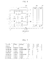
- FIG. 6 is a block diagram showing a configuration example of a conventional multiprocessor system.
- the conventional multiprocessor system includes a main memory 1, an SC (System Controller) 2, and one or more CPUs (Central Processing Unit) 103.
- the SC 2 is a main memory controller connected to the main memory 1 and all CPUs 103.
- the CPU 103 internally includes an L1 cache 4, an L2 cache 105, and a calculation unit 6.
- the L1 cache 4 is a primary cache of the CPU 103, and the L2 cache 105 is a secondary cache thereof.
- the L1 cache 4 includes an 11 cache 11 as an instruction cache and a D1 cache 12 as a data (operand) cache.
- the calculation unit 6 performs calculation using data of L1 cache 4.
- An L2 cache request (request to the L2 cache 105 issued from the L1 cache 4) includes a demand fetch request which is a normal readout operation from the main memory 1 and a prefetch request which is a speculative readout operation.
- the demand fetch request performs registration of data both in the L2 cache 105 and the L1 cache 4 which is a request source.
- the prefetch request performs data registration only in the L2 cache 105.
- FIG. 7 is a table showing an example of L2 cache requests.
- a cache block of the 11 cache 11 is managed by 11 TC (Type Cord) that assumes two states: V (Valid) and I (Invalid).
- a cache block of the D1 cache 12 is managed by D1 TC (Type Cord) that assumes three states: M (Modified), C (Clean), and I (Invalid).
- a cache block of the L2 cache 105 is managed by L2 TC (Type Cord) that assumes five states: M (Modified), O (Ownered), E (Exclusive), S (Shared), and I (Invalid).
- L2 cache requests for the demand fetch request IF-MI-SH, OP-MI-SH, and OP-MI-CH will be explained.
- the L1 cache 11 issues IF-MI-SH (L2 cache request for requesting a shared cache block) when an instruction fetch miss has occurred.
- IF-MI-SH L2 cache request for requesting a shared cache block
- the D1 cache 12 issues OP-MI-SH (L2 cache request for requesting a shared cache block) when an operand load miss has occurred. Further, the D1 cache 12 issues OP-MI-SH (L2 cache request for requesting a shared cache block) when an operand store miss has occurred. Further, the D1 cache 12 issues OP-MI-BL (L2 cache request called a block load that does not involve cache registration) for an operand load.
- OP-MI-SH L2 cache request for requesting a shared cache block
- OP-MI-BL L2 cache request called a block load that does not involve cache registration
- L2 cache requests for the prefetch request IF-PF-SH, OP-PF-SH, and OP-PF-EX are prepared in correspondence with the aforementioned L2 cache requests for the demand fetch request: IF-MI-SH, OP-MI-SH, and OP-MI-CH, respectively.
- the L1 cache 4 does not involve at all the prefetch request that the L1 cache 4 itself has issued.
- the L2 cache 105 can discard a prefetch request when it is difficult to perform prefetch processing, for example, in the case where there are many requests that have not been processed.
- the L2 cache 105 sends reply data to the L1 cache 4 when the L2 cache request is a cache hit.
- the L2 cache data 105 issues a move-in request P-Req to the SC 2 when the L2 cache request is a cache miss, and receives data S-Reply as a reply of the P-Req.
- the data S-Reply is then sent to the L1 cache 4 and is registered also in the L2 cache 105 at the same time.
- L2 cache request is OP-MI-CH
- registration is performed in M (modified) state even when a reply cache block is a clean one (write back to the memory is not necessary).
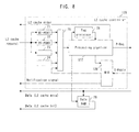
- FIG. 8 is a block diagram showing a configuration example of the conventional L2 cache.
- the L2 cache 105 is constituted by an L2 cache controller 120 and a data RAM 29.
- the L2 cache controller 120 includes an MI-PORT 21, a PF-PORT 22, other ports 23, 24, a priority section 25, a tag processor 26, a processing pipeline 127, and an MIB (Move-in Buffer) 128.
- MIB Move-in Buffer
- L2 cache request to the L2 cache 105 is firstly received by ports 21, 22, 23, and 24 that are associated with the L2 cache requests.
- the priority section 25 fetches the L2 cache requests remaining in the ports 21, 22, 23, and 24 and feeds the fetched requests into the processing pipeline 127.
- the processing pipeline 127 performs tag-search and tag-update operations in the tag processor 26, issues a reply to the L1 cache in response to the L2 cache request, ensures the MIB 128, and the like.
- the MIB 128 is a buffer for receiving cache miss data from the SC 2 and is ensured for each move-in processing.
- the MIB 128 is ensured at the cache miss time, then holds tag information, and is released upon completion of the corresponding move-in processing.
- the tag information includes a move-in request source, a move-in request address, a write back address to be replaced, and the like.
- the MIB 128 has a section that notifies the L1 cache 4 of move-in data arrival from the SC 2 and an abnormal end of the process for the move-in request address. Examples of a notification signal to the L1 cache 4 include a data valid signal, an error notification signal, and the like.
- the data RAM 29 stores data from the SC 2.
- the data from the SC 2 which has been obtained due to an L2 cache hit, is sent to the L1 cache 4.
- the data from the SC 2, which has been obtained due to an L2 cache miss is sent to the L1 cache 4 and at the same time, registered in the data RAM 29.
- FIG. 9 is a time chart showing an example of an operation of the L2 cache for a normal demand fetch request.
- the demand fetch request issued from the L1 cache 4 is stored in the MI-PORT 21, fetched in the priority section 25 and fed to the processing pipeline 127. Since the result obtained by performing a tag search with a read flow is cache miss in the case of FIG. 9 , the MIB 128 is ensured and a move-in request is issued to the SC 2. Move-in data from the SC 2 is immediately sent to the L1 cache 4 and at the same time is registered in the L2 cache 105 as a rule.
- FIG. 10 is a time chart showing an example of an operation of the L2 cache for a normal prefetch request.
- the prefetch request issued from the L1 cache 4 is stored in the PF-PORT 22, fetched in the priority section 25 and fed to the processing pipeline 127. Since the result of a tag search is cache miss in the case of FIG. 10 , the MIB 128 is ensured and a move-in request is issued to the SC 2. Move-in data from the SC 2 is registered only in the L2 cache 105, and the operation ends.
- Japanese Patent Application Laid-Open No. 2-133842 pages 4 to 6, FIG. 2 .
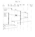
- FIG. 11 is a time chart showing an example of an operation of the conventional L2 cache in the case where a demand fetch request is issued immediately after issuance of a prefetch request.
- the prefetch and demand fetch requests are made for an address on the same cache block.
- the preceding prefetch request is fetched from the PF-PORT 22 and fed to the processing pipeline 127. Since the result of a tag search is cache miss in the case of FIG. 11 , the MIB is ensured and a request is issued to the SC 2.
- the succeeding demand fetch request is fetched from the MI-PORT 21. In this case, the request address is in a waiting state and processing does not proceed, with the result that the demand fetch request remains in the MI-PORT 21.
- a move-in data as a reply to the preceding prefetch request arrives, a cache block is registered in a tag, and the MIB 128 is released. After completion of the processing of the preceding prefetch request, a cache hit of the succeeding demand fetch request starts processing of the demand fetch.
- the present invention has been made to solve the above problem, and an object thereof is to provide a cache memory control unit that reduces waiting time in a demand fetch processing for a prefetch processing to be completed, a cache memory control method, a central processing unit, an information processor, and a central processing method.
- a cache memory control unit that controls a cache memory comprising: a request receiving section that receives a prefetch request and demand fetch request issued from a primary cache; and a swap processing section that performs swap processing when the request receiving section receives a demand fetch request designating the same memory address as that designated by a prefetch request that has already been received by the request receiving section, the swap processing being performed so that a move-in buffer that has been ensured for replying the prefetch request is used for a reply to the demand fetch request following the prefetch request.
- the swap processing section performs the swap processing by rewriting tag information of the move-in buffer.
- the swap processing section issues, to the primary cache, a prior notice indicating the arrival of a reply to the demand fetch request.
- the swap processing section issues, to the primary cache, a cancel of the prior notice when it has been determined, after the issuance of the prior notice during the swap determination period, that swap processing is not performed.
- the swap processing section performs the swap processing even when an error reply to the prefetch request has arrived during the swap determination period at which it is determined whether the swap processing is performed or not.
- the swap processing section delays issuance of the succeeding reply.
- the swap processing section performs the swap processing even when the demand fetch request is a request that need not to be registered in a secondary cache.
- a memory control method for controlling a cache memory comprising: a request receiving step of receiving a prefetch request and demanding fetch request issued from a primary cache; and a swap processing step of performing swap processing when the request receiving step receives a demand fetch request designating the same memory address as that designated by a prefetch request that has already been received in the request receiving step, the swap processing being performed so that a move-in buffer that has been ensured for replying the prefetch request is used for a reply to the demand fetch request following the prefetch request.
- the swap processing step performs the swap processing by rewriting tag information of the move-in buffer.
- the swap processing step issues, to the primary cache, a prior notice indicating the arrival of a reply to the demand fetch request.
- the swap processing step issues, to the primary cache, a cancel of the prior notice when it has been determined, after the issuance of the prior notice during the swap determination period, that swap processing is not performed.
- the swap processing step performs the swap processing even when an error reply to the prefetch request has arrived during the swap determination period at which it is determined whether the swap processing is performed or not.
- the swap processing step delays issuance of the succeeding reply.
- the swap processing step performs the swap processing even when the demand fetch request is a request that need not to be registered in a secondary cache.
- a central processing unit that performs control related to information processing comprising: a primary cache that issues a prefetch request and demand fetch request; a secondary cache that performs swap processing to allow a move-in buffer that has been ensured for replying the prefetch request to be used for a reply to the demand fetch request following the prefetch request; and a calculation section that performs calculation using data of the primary cache.
- the secondary cache performs the swap processing by rewriting tag information of the move-in buffer.
- the secondary cache issues, to the primary cache, a prior notice indicating the arrival of a reply to the demand fetch request.
- the secondary cache issues, to the primary cache, a cancel of the prior notice when it has been determined, after the issuance of the prior notice during the swap determination period, that swap processing is not performed.
- the secondary cache performs the swap processing even when an error reply to the prefetch request has arrived during the swap determination period at which it is determined whether the swap processing is performed or not.
- the secondary cache delays issuance of the succeeding reply.
- the secondary cache performs the swap processing even when the demand fetch request is a request that need not to be registered in the secondary cache.
- an information processor comprising: the one or more central processing units; a main storage section that stores data used by the central processing unit; and a main storage controller that manages data between the central processing unit and main storage section.
- a central processing method for performing control related to information processing comprising; a primary cache step of issuing a prefetch request and demanding fetch request; a secondary cache step of performing swap processing to allow a move-in buffer that has been ensured for replying the prefetch request to be used for a reply to the demand fetch request following the prefetch request; and a calculation step of performing calculation using data of the primary cache.
- the secondary cache step performs the swap processing by rewriting tag information of the move-in buffer.
- the secondary cache step issues, to the primary cache step, a prior notice indicating the arrival of a reply to the demand fetch request.
- the secondary cache step issues, to the primary cache step, a cancel of the prior notice when it has been determined, after the issuance of the prior notice during the swap determination period, that swap processing is not performed.
- the secondary cache step performs the swap processing even when an error reply to the prefetch request has arrived during the swap determination period at which it is determined whether the swap processing is performed or not.
- the secondary cache step delays issuance of the succeeding reply.
- the secondary cache step performs the swap processing even when the demand fetch request is a request that need not to be registered in the secondary cache step.
- the cache memory control unit corresponds to an L2 cache controller in the following embodiment
- the request receiving section corresponds to MI-PORT and PF-PORT in the following embodiment
- the swap processing section corresponds to a processing pipeline in the following embodiment
- the central processing unit corresponds to a CPU in the following embodiment
- the information processor corresponds to a multiprocessor system in the following embodiment
- the main storage corresponds to a main memory in the following embodiment
- the main storage controller corresponds to an SC in the following embodiment.
- waiting time in a demand fetch processing for a prefetch processing to be completed is reduced, thereby increasing memory access speed in the information processor.
- the present invention enables the MIB that has been ensured when a cache miss of a preceding prefetch request has occurred to be used for a succeeding demand fetch request.
- This processing is referred to as MIB swap processing.
- the MIB holds, as tag information, types of the requests that are issued from the L1 cache, the requests being factors by which the MIB itself is ensured.
- the above swap processing is realized by rewriting the tag information from the prefetch request to demand fetch request.
- FIG. 1 is a block diagram showing a configuration example of a multiprocessor system according to the present invention.
- the multiprocessor system of FIG. 1 includes a CPU 3 and an L2 cache 5 in place of the CPU 103 and L2 cache 105, respectively.
- FIG. 2 is a block diagram showing a configuration example of an L2 cache according to the present invention.
- the L2 cache of FIG. 2 includes an L2 cache controller 20, a processing pipeline 27, and an MIB 28 in place of the L2 cache controller 120, processing pipeline 127, and MIB 128, respectively.
- FIG. 3 is a time chart showing an operation of the L2 cache in the case where swap processing according to the present invention is performed. Firstly, a preceding prefetch request is fed from the PF-PORT 22 to the processing pipeline 27. Then a cache miss of the preceding prefetch request has occurred. In this case, the MIB 28 is ensured and P-Req is issued. Next, a succeeding demand fetch request for the same address is fed from the MI-PORT 21 to the processing pipeline 27. Then a cache miss also occurs in this case.
- the swap processing is performed such that the MIB 28 corresponding to the same address is apparently ensured by the demand fetch request.
- the reply data that has been sent from the SC 2 in response to the preceding prefetch request is then used by the succeeding demand fetch request. As a result, it is possible to immediately send data to the L1 cache 4.
- FIG. 4 is a table showing an example of combinations between prefetch and demand fetch that allows the swap processing according to the present invention to be performed.
- the MIB 28 that has been ensured by the prefetch request receives a reply cache block data from the SC 2 and starts to perform the data registration in the L2 cache 5
- this MIB 28 is not allowed to become a target of the swap processing.
- the reason is that since data is not sent to the L1 cache 4 in the case of the prefetch request, it is impossible to immediately send the received cache block to the L1 cache 4 even if swap processing has been performed.
- FIG. 5 is a block diagram showing a configuration example of a processing pipeline according to the present invention.
- the processing pipeline 27 includes an MIB address comparison section 31, a tag readout section 32, an MIB type cord determination section 33, an MIB swap determination section 34, an MIB swap section 35, and an MIB ensuring section 36.
- a request from the MI-PORT 21 or PF-PORT 22 is fed to the processing pipeline 27 as a read flow through the priority section 25.
- the MIB address comparison section 31 compares target addresses of a preceding request and succeeding request.
- the tag readout section 32 sends a tag to the tag processor 26, and the tag processor 26 then conducts a search. In the case of a cache hit, data is fed back to the L1 cache 4 (data is not fed back in the case of prefetch). In the case where a cache miss occurs, the MIB ensuring section 36 ensures the MIB 28 and issues a move-in request to the SC 2.
- a read flow for a demand fetch request is referred to as demand read.
- the MIB type cord determination section 33 determines whether a combination of the successive L2 cache requests is one of the combinations shown in FIG. 4 that allows the swap processing to be performed. When determining that the combination is one of the combinations that allow the swap processing to be performed, the MIB type cord determination section 33 sends the determination result as "swap possibility" to the MIB swap determination section 34.
- the MIB swap determination section 34 determines that the swap conditions are met based on "swap possibility" from the MIB type cord determination section 33 and demand_read of the processing pipeline 27 and the MIB swap section 35 then rewrites tag information of the MIB 28.
- the tag information that the MIB 28 holds includes "xreply”, “address”, “pf”, “opc”, and “swapped”.
- xreply indicates that the MIB 28 has received a reply from the SC 2;
- address indicates a request move-in address;
- pf indicates that the MIB has been ensured by prefetch;
- opc indicates a type of the request that has caused the MIB 28 to be ensured;
- “swapped” indicates that the swap processing has been performed such that the factor that has ensured the MIB 28 is switched from prefetch to demand fetch.
- Tb is a time period from the time at which the read flow performing swap processing has been fed to the processing pipeline 27 to the time before the swap processing has been started. This Tb is referred to as swap determination period.
- An update request to the MIB 28 is issued four cycles after the read flow has been fed to the processing pipeline 27.
- a processing flow is assumed to be fed to the processing pipeline 27 every two cycle.
- the read flow itself may be disrupted due to detection of a correctable error or the like. In this case, swap processing cannot be realized and the tag information of the MIB 28 is not updated accordingly.
- Tc is a time period from the time at which the CPU 3 has received a reply from the SC 2 to the time at which the tag information "xreply" indicating that the MIB 28, which is a request source, has received the reply has been set.
- time periods Tc and Tb are overlapped, that is, when the demand_read having "swap possibility" is newly fed to the processing pipeline 27 for the same MIB, the arrived move-in data is immediately transferred to the L1 cache 4 after completion of swap processing. If the swap processing has not been performed, which means prefetch processing, notification to the L1 cache 4 is not issued.
- the MIB 28 In the L2 cache 5 according to the present invention generates, the MIB 28 generates a data valid signal (DOW-fr-SC) and a cancel signal (DOW-CAN-fr-SC) thereof in order to notify the L1 cache 4 of the arrived move-in data.
- DOW-fr-SC indicates that a request move-in data has arrived in the L2 cache 5 from the SC 2.
- DOW-CAN-fr-SC indicates that DOW-fr-SC that had been issued several cycles before (here, three cycles before) has become invalid.
- the MIB 28 as a request source that should receives a move-in data at the time when the L2 cache 5 has received the move-in data from the SC 2 is referred to as current MIB.
- an error notification is issued to the L1 cache 4 when the swap processing has been completed and the request has been handled as demand fetch processing, whereas an error notification is not issued to the L1 cache 4 when the swap processing is not effected and the request has been handled as prefetch processing.
- the MIB 28 of the L2 cache 5 generates an error notification signal and issues the signal to the L1 cache 4.
- an error notification to the L1 cache is not performed with respect to an error reply that the MIB ensured by a prefetch request has been received.
- an error notification must be performed in the case where swap processing has been made.
- the MIB 28 that has been ensured by a prefetch request has received an error reply, it refers to tag information "swapped" thereof three cycles after the reception of the error reply.
- the MIB 28 performs notification to the L1 cache 4.
- the time corresponding to the above three cycles is the time required to set a determination result in the tag information of the MIB 28 when the MIB 28 that has received an error reply from the SC 2 (at this time point, tag information "xreply" has not been set and the MIB 28 may become a target of swap processing) is a target of swap determination in the processing pipeline 27.
- an error notification signal is issued behind a normal error notification signal.
- the error notification signal that has issued behind and the succeeding normal error signal collide with each other, issuance of the succeeding error notification signal is delayed.
Abstract
Description
- The present invention relates to a cache memory control unit having a primary cache and a secondary cache, a cache memory control method, a central processing unit, an information processor, and a central processing method.
-
FIG. 6 is a block diagram showing a configuration example of a conventional multiprocessor system. The conventional multiprocessor system includes amain memory 1, an SC (System Controller) 2, and one or more CPUs (Central Processing Unit) 103. TheSC 2 is a main memory controller connected to themain memory 1 and allCPUs 103. TheCPU 103 internally includes anL1 cache 4, anL2 cache 105, and acalculation unit 6. TheL1 cache 4 is a primary cache of theCPU 103, and theL2 cache 105 is a secondary cache thereof. TheL1 cache 4 includes an 11cache 11 as an instruction cache and aD1 cache 12 as a data (operand) cache. Thecalculation unit 6 performs calculation using data ofL1 cache 4. - As a method for hiding latency in CPU memory access, a prefetch operation has been widely used. With this method, the area in a main memory that is likely to be used is previously "moved-in" (data of the main memory is previously registered in a cache), thereby reducing cache miss rate.
- An L2 cache request (request to the
L2 cache 105 issued from the L1 cache 4) includes a demand fetch request which is a normal readout operation from themain memory 1 and a prefetch request which is a speculative readout operation. The demand fetch request performs registration of data both in theL2 cache 105 and theL1 cache 4 which is a request source. On the other hand, the prefetch request performs data registration only in theL2 cache 105. - Next, a description will be given of the types of the L2 cache requests.
FIG. 7 is a table showing an example of L2 cache requests. Here, a cache block of the 11cache 11 is managed by 11 TC (Type Cord) that assumes two states: V (Valid) and I (Invalid). A cache block of theD1 cache 12 is managed by D1 TC (Type Cord) that assumes three states: M (Modified), C (Clean), and I (Invalid). A cache block of theL2 cache 105 is managed by L2 TC (Type Cord) that assumes five states: M (Modified), O (Ownered), E (Exclusive), S (Shared), and I (Invalid). - Firstly, L2 cache requests for the demand fetch request: IF-MI-SH, OP-MI-SH, and OP-MI-CH will be explained.
- The L1 cache 11 issues IF-MI-SH (L2 cache request for requesting a shared cache block) when an instruction fetch miss has occurred.
- The D1 cache 12 issues OP-MI-SH (L2 cache request for requesting a shared cache block) when an operand load miss has occurred. Further, the D1 cache 12 issues OP-MI-SH (L2 cache request for requesting a shared cache block) when an operand store miss has occurred. Further, the D1 cache 12 issues OP-MI-BL (L2 cache request called a block load that does not involve cache registration) for an operand load.
- In order to increase L2 cache hit rate at the time of L1 cache miss, L2 cache requests for the prefetch request: IF-PF-SH, OP-PF-SH, and OP-PF-EX are prepared in correspondence with the aforementioned L2 cache requests for the demand fetch request: IF-MI-SH, OP-MI-SH, and OP-MI-CH, respectively.
- The
L1 cache 4 does not involve at all the prefetch request that theL1 cache 4 itself has issued. TheL2 cache 105 can discard a prefetch request when it is difficult to perform prefetch processing, for example, in the case where there are many requests that have not been processed. - An operation between the
L2 cache 105 andSC 2 will next be described. TheL2 cache 105 sends reply data to theL1 cache 4 when the L2 cache request is a cache hit. On the other hand, theL2 cache data 105 issues a move-in request P-Req to theSC 2 when the L2 cache request is a cache miss, and receives data S-Reply as a reply of the P-Req. The data S-Reply is then sent to theL1 cache 4 and is registered also in theL2 cache 105 at the same time. - When P-Req from the
L2 cache 105 to theSC 2 is P-RDSA (robust shared type), S-RBS (shared type) is returned as S-Reply from theSC 2 to theL2 cache 105. When P-Req is P-RDS (shared type), S-RBS (shared type) or S-RBU (exclusive type) is returned as S-Reply. When P-Req is P-RDO (exclusive type), S-RBU is returned as S-Reply. - When L2 cache request is OP-MI-CH, registration is performed in M (modified) state even when a reply cache block is a clean one (write back to the memory is not necessary).
- When L2 cache request OP-MI-BL results in L2 cache miss, P-RDD (discard type request that does not involve invalidation of other cache blocks or data-sharing) is issued from the
L2 cache 105 to theSC 2. - A configuration of the
L2 cache 105 will next be described.FIG. 8 is a block diagram showing a configuration example of the conventional L2 cache. TheL2 cache 105 is constituted by anL2 cache controller 120 and adata RAM 29. TheL2 cache controller 120 includes an MI-PORT 21, a PF-PORT 22,other ports priority section 25, atag processor 26, aprocessing pipeline 127, and an MIB (Move-in Buffer) 128. - L2 cache request to the
L2 cache 105 is firstly received byports priority section 25 fetches the L2 cache requests remaining in theports processing pipeline 127. Theprocessing pipeline 127 performs tag-search and tag-update operations in thetag processor 26, issues a reply to the L1 cache in response to the L2 cache request, ensures theMIB 128, and the like. TheMIB 128 is a buffer for receiving cache miss data from theSC 2 and is ensured for each move-in processing. - The
MIB 128 is ensured at the cache miss time, then holds tag information, and is released upon completion of the corresponding move-in processing. The tag information includes a move-in request source, a move-in request address, a write back address to be replaced, and the like. TheMIB 128 has a section that notifies theL1 cache 4 of move-in data arrival from theSC 2 and an abnormal end of the process for the move-in request address. Examples of a notification signal to theL1 cache 4 include a data valid signal, an error notification signal, and the like. Thedata RAM 29 stores data from theSC 2. The data from theSC 2, which has been obtained due to an L2 cache hit, is sent to theL1 cache 4. The data from theSC 2, which has been obtained due to an L2 cache miss is sent to theL1 cache 4 and at the same time, registered in thedata RAM 29. - A normal demand fetch operation will next be described.
FIG. 9 is a time chart showing an example of an operation of the L2 cache for a normal demand fetch request. The demand fetch request issued from theL1 cache 4 is stored in the MI-PORT 21, fetched in thepriority section 25 and fed to theprocessing pipeline 127. Since the result obtained by performing a tag search with a read flow is cache miss in the case ofFIG. 9 , theMIB 128 is ensured and a move-in request is issued to theSC 2. Move-in data from theSC 2 is immediately sent to theL1 cache 4 and at the same time is registered in theL2 cache 105 as a rule. - A normal prefetch operation will next be described.
FIG. 10 is a time chart showing an example of an operation of the L2 cache for a normal prefetch request. The prefetch request issued from theL1 cache 4 is stored in the PF-PORT 22, fetched in thepriority section 25 and fed to theprocessing pipeline 127. Since the result of a tag search is cache miss in the case ofFIG. 10 , theMIB 128 is ensured and a move-in request is issued to theSC 2. Move-in data from theSC 2 is registered only in theL2 cache 105, and the operation ends. - As a reference of the related art, Japanese Patent Application Laid-Open No.
2-133842 pages 4 to 6,FIG. 2 ) is known. - In the aforementioned conventional L2 cache, when an MIB being in a move-in stand-by state and having the same memory address as that of a request that has been fed to the
processing pipeline 127 exists, processing of the request in theprocessing pipeline 127 is disrupted and the request is allowed to remain in the port so that a move-in request for the same address is not issued during the time between an issuance of the move-in request to theSC 2 and arrival of a reply from theSC 2. -
FIG. 11 is a time chart showing an example of an operation of the conventional L2 cache in the case where a demand fetch request is issued immediately after issuance of a prefetch request. The prefetch and demand fetch requests are made for an address on the same cache block. The preceding prefetch request is fetched from the PF-PORT 22 and fed to theprocessing pipeline 127. Since the result of a tag search is cache miss in the case ofFIG. 11 , the MIB is ensured and a request is issued to theSC 2. The succeeding demand fetch request is fetched from the MI-PORT 21. In this case, the request address is in a waiting state and processing does not proceed, with the result that the demand fetch request remains in the MI-PORT 21. After that, a move-in data as a reply to the preceding prefetch request arrives, a cache block is registered in a tag, and theMIB 128 is released. After completion of the processing of the preceding prefetch request, a cache hit of the succeeding demand fetch request starts processing of the demand fetch. - That is, although the demand fetch request has been issued from the
L1 cache 4 and the move-in data has arrived from theSC 2, data cannot be directly passed to theL1 cache 4 since the move-in data is a reply to the prefetch request, with the result that the data is registered only in theL2 cache 105. When the demand fetch request is fed to the processing pipeline after completion of the move-in to the prefetch request, the data that has been registered in theL2 cache 105 is sent to theL1 cache 4. Therefore, waiting time for the prefetch processing to be completed is generated in the demand fetch processing. - The present invention has been made to solve the above problem, and an object thereof is to provide a cache memory control unit that reduces waiting time in a demand fetch processing for a prefetch processing to be completed, a cache memory control method, a central processing unit, an information processor, and a central processing method.
- To solve the above problem, according to a first aspect of the present invention, there is provided a cache memory control unit that controls a cache memory comprising: a request receiving section that receives a prefetch request and demand fetch request issued from a primary cache; and a swap processing section that performs swap processing when the request receiving section receives a demand fetch request designating the same memory address as that designated by a prefetch request that has already been received by the request receiving section, the swap processing being performed so that a move-in buffer that has been ensured for replying the prefetch request is used for a reply to the demand fetch request following the prefetch request.
- In the cache memory control unit according to the present invention, the swap processing section performs the swap processing by rewriting tag information of the move-in buffer.
- In the cache memory control unit according to the present invention, when a correct reply to the prefetch request has arrived during a swap determination period at which it is determined whether the swap processing is performed or not, the swap processing section issues, to the primary cache, a prior notice indicating the arrival of a reply to the demand fetch request.
- In the cache memory control unit according to the present invention, the swap processing section issues, to the primary cache, a cancel of the prior notice when it has been determined, after the issuance of the prior notice during the swap determination period, that swap processing is not performed.
- In the cache memory control unit according to the present invention, the swap processing section performs the swap processing even when an error reply to the prefetch request has arrived during the swap determination period at which it is determined whether the swap processing is performed or not.
- In the cache memory control unit according to the present invention, when the error reply is delayed by the swap processing and thereby the error reply and a succeeding reply collide with each other, the swap processing section delays issuance of the succeeding reply.
- In the cache memory control unit according to the present invention, the swap processing section performs the swap processing even when the demand fetch request is a request that need not to be registered in a secondary cache.
- According to a second aspect of the present invention, there is provided a memory control method for controlling a cache memory comprising: a request receiving step of receiving a prefetch request and demanding fetch request issued from a primary cache; and a swap processing step of performing swap processing when the request receiving step receives a demand fetch request designating the same memory address as that designated by a prefetch request that has already been received in the request receiving step, the swap processing being performed so that a move-in buffer that has been ensured for replying the prefetch request is used for a reply to the demand fetch request following the prefetch request.
- In the cache memory control method according to the present invention, the swap processing step performs the swap processing by rewriting tag information of the move-in buffer.
- In the cache memory control method according to the present invention, when a correct reply to the prefetch request has arrived during a swap determination period at which it is determined whether the swap processing is performed or not, the swap processing step issues, to the primary cache, a prior notice indicating the arrival of a reply to the demand fetch request.
- In the cache memory control method according to the present invention, the swap processing step issues, to the primary cache, a cancel of the prior notice when it has been determined, after the issuance of the prior notice during the swap determination period, that swap processing is not performed.
- In the cache memory control method according to the present invention, the swap processing step performs the swap processing even when an error reply to the prefetch request has arrived during the swap determination period at which it is determined whether the swap processing is performed or not.
- In the cache memory control method according to the present invention, when the error reply is delayed by the swap processing and thereby the error reply and a succeeding reply collide with each other, the swap processing step delays issuance of the succeeding reply.
- In the cache memory control method according to the present invention, the swap processing step performs the swap processing even when the demand fetch request is a request that need not to be registered in a secondary cache.
- According to a third aspect of the present invention, there is provided a central processing unit that performs control related to information processing comprising: a primary cache that issues a prefetch request and demand fetch request; a secondary cache that performs swap processing to allow a move-in buffer that has been ensured for replying the prefetch request to be used for a reply to the demand fetch request following the prefetch request; and a calculation section that performs calculation using data of the primary cache.
- In the central processing unit according to the present invention, the secondary cache performs the swap processing by rewriting tag information of the move-in buffer.
- In the central processing unit according to the present invention, when a correct reply to the prefetch request has arrived during a swap determination period at which it is determined whether the swap processing is performed or not, the secondary cache issues, to the primary cache, a prior notice indicating the arrival of a reply to the demand fetch request.
- In the central processing unit according to the present invention, the secondary cache issues, to the primary cache, a cancel of the prior notice when it has been determined, after the issuance of the prior notice during the swap determination period, that swap processing is not performed.
- In the central processing unit according to the present invention, the secondary cache performs the swap processing even when an error reply to the prefetch request has arrived during the swap determination period at which it is determined whether the swap processing is performed or not.
- In the central processing unit according to the present invention, when the error reply is delayed by the swap processing and thereby the error reply and a succeeding reply collide with each other, the secondary cache delays issuance of the succeeding reply.
- In the central processing unit according to the present invention, the secondary cache performs the swap processing even when the demand fetch request is a request that need not to be registered in the secondary cache.
- According to a fourth aspect of the present invention, there is provided an information processor comprising: the one or more central processing units; a main storage section that stores data used by the central processing unit; and a main storage controller that manages data between the central processing unit and main storage section.
- According to a fifth aspect of the present invention, there is provided a central processing method for performing control related to information processing comprising; a primary cache step of issuing a prefetch request and demanding fetch request; a secondary cache step of performing swap processing to allow a move-in buffer that has been ensured for replying the prefetch request to be used for a reply to the demand fetch request following the prefetch request; and a calculation step of performing calculation using data of the primary cache.
- In the central processing method according to the present invention, the secondary cache step performs the swap processing by rewriting tag information of the move-in buffer.
- In the central processing method according to the present invention, when a correct reply to the prefetch request has arrived during a swap determination period at which it is determined whether the swap processing is performed or not, the secondary cache step issues, to the primary cache step, a prior notice indicating the arrival of a reply to the demand fetch request.
- In the central processing method according to the present invention, the secondary cache step issues, to the primary cache step, a cancel of the prior notice when it has been determined, after the issuance of the prior notice during the swap determination period, that swap processing is not performed.
- In the central processing method according to the present invention, the secondary cache step performs the swap processing even when an error reply to the prefetch request has arrived during the swap determination period at which it is determined whether the swap processing is performed or not.
- In the central processing method according to the present invention, when the error reply is delayed by the swap processing and thereby the error reply and a succeeding reply collide with each other, the secondary cache step delays issuance of the succeeding reply.
- In the central processing method according to the present invention, the secondary cache step performs the swap processing even when the demand fetch request is a request that need not to be registered in the secondary cache step.
- Note that the cache memory control unit corresponds to an L2 cache controller in the following embodiment; the request receiving section corresponds to MI-PORT and PF-PORT in the following embodiment; the swap processing section corresponds to a processing pipeline in the following embodiment; the central processing unit corresponds to a CPU in the following embodiment; the information processor corresponds to a multiprocessor system in the following embodiment; the main storage corresponds to a main memory in the following embodiment; and the main storage controller corresponds to an SC in the following embodiment.
- According to the present invention, waiting time in a demand fetch processing for a prefetch processing to be completed is reduced, thereby increasing memory access speed in the information processor.
-
-
FIG. 1 is a block diagram showing a configuration example of a multiprocessor system according to the present invention; -
FIG. 2 is a block diagram showing a configuration example of an L2 cache according to the present invention; -
FIG. 3 is a time chart showing an operation of the L2 cache in the case where swap processing according to the present invention is performed; -
FIG. 4 is a table showing an example of combinations between prefetch and demand fetch that allows the swap processing according to the present invention to be performed; -
FIG. 5 is a block diagram showing a configuration example of a processing pipeline according to the present invention; -
FIG. 6 is a block diagram showing a configuration example of a conventional multiprocessor system; -
FIG. 7 is a table showing an example of L2 cache requests; -
FIG. 8 is a block diagram showing a configuration example of the conventional L2 cache; -
FIG. 9 is a time chart showing an example of an operation of the L2 cache for a normal demand fetch request; -
FIG. 10 is a time chart showing an example of an operation of the L2 cache for a normal prefetch request; and -
FIG. 11 is a time chart showing an example of an operation of the conventional L2 cache in the case where a demand fetch request is issued immediately after issuance of a prefetch request. - An embodiment of the present invention will be described below with reference to the accompanying drawings.
- The present invention enables the MIB that has been ensured when a cache miss of a preceding prefetch request has occurred to be used for a succeeding demand fetch request. This processing is referred to as MIB swap processing. More specifically, the MIB holds, as tag information, types of the requests that are issued from the L1 cache, the requests being factors by which the MIB itself is ensured. The above swap processing is realized by rewriting the tag information from the prefetch request to demand fetch request.
-
FIG. 1 is a block diagram showing a configuration example of a multiprocessor system according to the present invention. InFIG. 1 , the same reference numerals as those inFIG. 6 denote the same or corresponding parts as those inFIG. 6 , and the descriptions thereof will be omitted here. The multiprocessor system ofFIG. 1 includes aCPU 3 and anL2 cache 5 in place of theCPU 103 andL2 cache 105, respectively. -
FIG. 2 is a block diagram showing a configuration example of an L2 cache according to the present invention. InFIG. 2 , the same reference numerals as those inFIG. 8 denote the same or corresponding parts as those inFIG. 8 , and the descriptions thereof will be omitted here. The L2 cache ofFIG. 2 includes anL2 cache controller 20, aprocessing pipeline 27, and anMIB 28 in place of theL2 cache controller 120,processing pipeline 127, andMIB 128, respectively. -
FIG. 3 is a time chart showing an operation of the L2 cache in the case where swap processing according to the present invention is performed. Firstly, a preceding prefetch request is fed from the PF-PORT 22 to theprocessing pipeline 27. Then a cache miss of the preceding prefetch request has occurred. In this case, theMIB 28 is ensured and P-Req is issued. Next, a succeeding demand fetch request for the same address is fed from the MI-PORT 21 to theprocessing pipeline 27. Then a cache miss also occurs in this case. Here, the swap processing is performed such that theMIB 28 corresponding to the same address is apparently ensured by the demand fetch request. The reply data that has been sent from theSC 2 in response to the preceding prefetch request is then used by the succeeding demand fetch request. As a result, it is possible to immediately send data to theL1 cache 4. - The above swap processing can be performed only in the case of the combination of requests that allows the processing performed when the
MIB 28 is ensured due to a cache miss of the prefetch request to be taken over by the succeeding demand fetch request.FIG. 4 is a table showing an example of combinations between prefetch and demand fetch that allows the swap processing according to the present invention to be performed. - Here, even when a block load OP-MI-BL is performed for the same address as the prefetch request, it is possible to complete the swap processing. In this case, in order to maintain compatibility (processing for the cache block to be replaced) with the preceding prefetch request, data registration in the
L2 cache 5, which is not made in the normal block load, is performed. - In the case where the
MIB 28 that has been ensured by the prefetch request receives a reply cache block data from theSC 2 and starts to perform the data registration in theL2 cache 5, thisMIB 28 is not allowed to become a target of the swap processing. The reason is that since data is not sent to theL1 cache 4 in the case of the prefetch request, it is impossible to immediately send the received cache block to theL1 cache 4 even if swap processing has been performed. - Here, a description will be given of combinations of requests other than those shown in the table of
FIG. 4 , that is, the combination that the swap processing cannot be applied to. - Firstly, in the case where a preceding prefetch request is IF-PF-SH or OP-PF-SH, and a succeeding demand prefetch request is OP-MI-CH, swap processing cannot be performed. The reason is that, an L2 cache registration assumes S type in the preceding prefetch in some cases as shown in
FIG. 7 , whereas an L2 cache registration always assumes E type in the succeeding demand fetch, so that consistency between caches cannot be maintained. - Further, in the case where a succeeding demand fetch is IF-MI-SH, the swap processing cannot be performed. The reason is that although an L2 cache registration always assumes S type since P-Req that is issued at the time of a cache miss of IF-MI-SH is P-RDSA as shown in
FIG. 7 , there is a possibility that an L2 cache registration assumes E type or M type depending on the type of P-Req that has been issued due to a cache miss of a preceding prefetch request, so that consistency between caches cannot be maintained. - Further, in the case where the succeeding demand fetch is OP-MI-SH, the swap processing cannot be performed. The reason is that although an L2 cache registration of OP-MI-SH assumes S type or E type as shown in
FIG. 7 , an L2 cache registration assumes M type when the preceding prefetch request is OP-PF-EX, so that consistency between caches cannot be maintained. -
FIG. 5 is a block diagram showing a configuration example of a processing pipeline according to the present invention. Theprocessing pipeline 27 includes an MIBaddress comparison section 31, atag readout section 32, an MIB typecord determination section 33, an MIBswap determination section 34, anMIB swap section 35, and anMIB ensuring section 36. - A request from the MI-
PORT 21 or PF-PORT 22 is fed to theprocessing pipeline 27 as a read flow through thepriority section 25. The MIBaddress comparison section 31 compares target addresses of a preceding request and succeeding request. - The
tag readout section 32 sends a tag to thetag processor 26, and thetag processor 26 then conducts a search. In the case of a cache hit, data is fed back to the L1 cache 4 (data is not fed back in the case of prefetch). In the case where a cache miss occurs, theMIB ensuring section 36 ensures theMIB 28 and issues a move-in request to theSC 2. A read flow for a demand fetch request is referred to as demand read. - Then a possibility of swap processing is detected for each MIB. The MIB type
cord determination section 33 determines whether a combination of the successive L2 cache requests is one of the combinations shown inFIG. 4 that allows the swap processing to be performed. When determining that the combination is one of the combinations that allow the swap processing to be performed, the MIB typecord determination section 33 sends the determination result as "swap possibility" to the MIBswap determination section 34. The MIBswap determination section 34 determines that the swap conditions are met based on "swap possibility" from the MIB typecord determination section 33 and demand_read of theprocessing pipeline 27 and theMIB swap section 35 then rewrites tag information of theMIB 28. - The tag information that the
MIB 28 holds includes "xreply", "address", "pf", "opc", and "swapped". "xreply" indicates that theMIB 28 has received a reply from theSC 2; "address" indicates a request move-in address; "pf" indicates that the MIB has been ensured by prefetch; "opc" indicates a type of the request that has caused theMIB 28 to be ensured; "swapped" indicates that the swap processing has been performed such that the factor that has ensured theMIB 28 is switched from prefetch to demand fetch. - In
FIG. 3 , Tb is a time period from the time at which the read flow performing swap processing has been fed to theprocessing pipeline 27 to the time before the swap processing has been started. This Tb is referred to as swap determination period. An update request to theMIB 28 is issued four cycles after the read flow has been fed to theprocessing pipeline 27. A processing flow is assumed to be fed to theprocessing pipeline 27 every two cycle. - The read flow itself may be disrupted due to detection of a correctable error or the like. In this case, swap processing cannot be realized and the tag information of the
MIB 28 is not updated accordingly. - When two demand_read having "swap possibility" are sequentially fed to the
processing pipeline 27, "swap possibility" may be detected two times. To avoid this, when a preceding processing flow that has been issued two cycles before is processing for the same address and performs update of the tag information of theMIB 28, the swap processing of a succeeding processing flow is prevented. - In
FIG. 3 , Tc is a time period from the time at which theCPU 3 has received a reply from theSC 2 to the time at which the tag information "xreply" indicating that theMIB 28, which is a request source, has received the reply has been set. In the case where time periods Tc and Tb are overlapped, that is, when the demand_read having "swap possibility" is newly fed to theprocessing pipeline 27 for the same MIB, the arrived move-in data is immediately transferred to theL1 cache 4 after completion of swap processing. If the swap processing has not been performed, which means prefetch processing, notification to theL1 cache 4 is not issued. - To realize this, when move-in data has arrived while the read flow having "swap possibility" flows in the
processing pipeline 27, a prior notice indicating arrival of the move-in data is given to theL1 cache 4 and a cancel signal is issued to theL1 cache 4 if swap processing has not been performed afterward. - In the
L2 cache 5 according to the present invention generates, theMIB 28 generates a data valid signal (DOW-fr-SC) and a cancel signal (DOW-CAN-fr-SC) thereof in order to notify theL1 cache 4 of the arrived move-in data. DOW-fr-SC indicates that a request move-in data has arrived in theL2 cache 5 from theSC 2. DOW-CAN-fr-SC indicates that DOW-fr-SC that had been issued several cycles before (here, three cycles before) has become invalid. TheMIB 28 as a request source that should receives a move-in data at the time when theL2 cache 5 has received the move-in data from theSC 2 is referred to as current MIB. - In the prior art, when a move-in data, which originates not in a prefetch request but in a demand fetch request, arrives, DOW-fr-SC has been used as a valid signal. On the other hand, in the present invention, when the current MIB has "swap possibility", issuance of DOW-fr-SC is permitted. Then, at three cycles after the time when the issuance of DOW-fr-SC has been permitted due to "swap possibility", swapped tag information of the current MIB is referred to. If the swap processing has not been performed, which means prefetch processing, DOW-CAN-fr-SC is issued and the previously issued DOW-fr-SC is canceled.
- In the case where an error reply has arrived from the
SC 2 during the swap determination period, an error notification is issued to theL1 cache 4 when the swap processing has been completed and the request has been handled as demand fetch processing, whereas an error notification is not issued to theL1 cache 4 when the swap processing is not effected and the request has been handled as prefetch processing. - To realize the above processing, the
MIB 28 of theL2 cache 5 according to the present invention generates an error notification signal and issues the signal to theL1 cache 4. - In the prior art, an error notification to the L1 cache is not performed with respect to an error reply that the MIB ensured by a prefetch request has been received. However, in the present invention, an error notification must be performed in the case where swap processing has been made. Thus, when the
MIB 28 that has been ensured by a prefetch request has received an error reply, it refers to tag information "swapped" thereof three cycles after the reception of the error reply. When determining that swap processing has been performed, theMIB 28 performs notification to theL1 cache 4. The time corresponding to the above three cycles is the time required to set a determination result in the tag information of theMIB 28 when theMIB 28 that has received an error reply from the SC 2 (at this time point, tag information "xreply" has not been set and theMIB 28 may become a target of swap processing) is a target of swap determination in theprocessing pipeline 27. - As described above, when swap processing has been applied to the
MIB 28 that had received an error reply, an error notification signal is issued behind a normal error notification signal. When the error notification signal that has issued behind and the succeeding normal error signal collide with each other, issuance of the succeeding error notification signal is delayed.
Claims (13)
- A central processing unit that performs control related to information processing comprising:a primary cache that issues a prefetch request and demand fetch request;a secondary cache that performs swap processing to allow a move-in buffer that has been ensured for replying the prefetch request to be used for a reply to the demand fetch request following the prefetch request, swap processing being performed only in the case of the combination of requests that allows the processing performed when the move-in buffer is ensured to be taken over by the succeeding demand fetch request; anda calculation section that performs calculation using data of the primary cache;wherein, when a correct reply to the prefetch request has arrived during a swap determination period at which it is determined whether the swap processing is performed or not, the secondary cache issues, to the primary cache, a prior notice indicating the arrival of a reply to the demand fetch request.
- The central processing unit according to claim 1, wherein the secondary cache performs the swap processing by rewriting tag information of the move-in buffer.
- The central processing unit according to claim 1, wherein the secondary cache issues, to the primary cache, a cancel of the prior notice when it has been determined, after the issuance of the prior notice during the swap determination period, that swap processing is not performed.
- The central processing unit according to claim 1, wherein the secondary cache performs the swap processing even when an error reply to the prefetch request has arrived during the swap determination period at which it is determined whether the swap processing is performed or not.
- The central processing unit according to claim 4, wherein, when the error reply is delayed by the swap processing and thereby the error reply and a succeeding reply collide with each other, the secondary cache delays issuance of the succeeding reply.
- The central processing unit according to claim 1, wherein the secondary cache performs the swap processing even when the demand fetch request is a request that need not to be registered in the secondary cache.
- An information processor comprising:a central processing unit as claimed in claim 1;a main storage section that stores data used by the central processing unit; anda main storage controller that manages data between the central processing unit and main storage section.
- A central processing method for performing control related to information processing comprising;a primary cache step of issuing a prefetch request and demanding fetch request;a secondary cache step of performing swap processing to allow a move-in buffer that has been ensured for replying the prefetch request to be used for a reply to the demand fetch request following the prefetch request, swap processing being performed only in the case of the combination of requests that allows the processing performed when the move-in buffer is ensured to be taken over by the succeeding demand fetch request; anda calculation step of performing calculation using data of the primary cache;wherein, when a correct reply to the prefetch request has arrived during a swap determination period at which it is determined whether the swap processing is performed or not, the secondary cache step issues, to the primary cache step, a prior notice indicating the arrival of a reply to the demand fetch request.
- The central processing method according to claim 8, wherein the secondary cache step performs the swap processing by rewriting tag information of the move-in buffer.
- The central processing method according to claim 8, wherein the secondary cache step issues, to the primary cache step, a cancel of the prior notice when it has been determined, after the issuance of the prior notice during the swap determination period, that swap processing is not performed.
- The central processing method according to claim 8, wherein the secondary cache step performs the swap processing even when an error reply to the prefetch request has arrived during the swap determination period at which it is determined whether the swap processing is performed or not.
- The central processing method according to claim 11, wherein, when the error reply is delayed by the swap processing and thereby the error reply and a succeeding reply collide with each other, the secondary cache step delays issuance of the succeeding reply.
- The central processing method according to claim 8, wherein the secondary cache step performs the swap processing even when the demand fetch request is a request that need not to be registered in the secondary cache step.
Applications Claiming Priority (2)
| Application Number | Priority Date | Filing Date | Title |
|---|---|---|---|
| JP2004221156A JP4575065B2 (en) | 2004-07-29 | 2004-07-29 | Cache memory control device, cache memory control method, central processing unit, information processing device, central control method |
| EP04257182A EP1622026B1 (en) | 2004-07-29 | 2004-11-19 | Cache memory control unit and cache memory control method |
Related Parent Applications (2)
| Application Number | Title | Priority Date | Filing Date |
|---|---|---|---|
| EP04257182A Division EP1622026B1 (en) | 2004-07-29 | 2004-11-19 | Cache memory control unit and cache memory control method |
| EP04257182.8 Division | 2004-11-19 |
Publications (3)
| Publication Number | Publication Date |
|---|---|
| EP1942416A2 true EP1942416A2 (en) | 2008-07-09 |
| EP1942416A3 EP1942416A3 (en) | 2008-09-03 |
| EP1942416B1 EP1942416B1 (en) | 2011-06-29 |
Family
ID=35170065
Family Applications (2)
| Application Number | Title | Priority Date | Filing Date |
|---|---|---|---|
| EP08152649A Expired - Fee Related EP1942416B1 (en) | 2004-07-29 | 2004-11-19 | Central processing unit, information processor and central processing method |
| EP04257182A Expired - Fee Related EP1622026B1 (en) | 2004-07-29 | 2004-11-19 | Cache memory control unit and cache memory control method |
Family Applications After (1)
| Application Number | Title | Priority Date | Filing Date |
|---|---|---|---|
| EP04257182A Expired - Fee Related EP1622026B1 (en) | 2004-07-29 | 2004-11-19 | Cache memory control unit and cache memory control method |
Country Status (4)
| Country | Link |
|---|---|
| US (1) | US7552287B2 (en) |
| EP (2) | EP1942416B1 (en) |
| JP (1) | JP4575065B2 (en) |
| DE (1) | DE602004018913D1 (en) |
Families Citing this family (11)
| Publication number | Priority date | Publication date | Assignee | Title |
|---|---|---|---|---|
| CN101681304B (en) | 2007-06-20 | 2012-07-04 | 富士通株式会社 | Cash memory control device and pipeline control method |
| US8171225B2 (en) * | 2007-06-28 | 2012-05-01 | Intel Corporation | Cache for a multi thread and multi core system and methods thereof |
| JPWO2009096161A1 (en) * | 2008-01-29 | 2011-05-26 | パナソニック株式会社 | Processor performance analysis apparatus, method and simulator |
| JP4843717B2 (en) | 2008-02-18 | 2011-12-21 | 富士通株式会社 | Arithmetic processing device and control method of arithmetic processing device |
| JP2010191754A (en) * | 2009-02-19 | 2010-09-02 | Mitsubishi Electric Corp | Cache storage |
| JP5444889B2 (en) * | 2009-06-30 | 2014-03-19 | 富士通株式会社 | Arithmetic processing device and control method of arithmetic processing device |
| JP5609092B2 (en) * | 2009-12-09 | 2014-10-22 | 富士通株式会社 | Arithmetic processing device and control method of arithmetic processing device |
| JP5482801B2 (en) | 2009-12-25 | 2014-05-07 | 富士通株式会社 | Arithmetic processing unit |
| JP5730126B2 (en) | 2011-05-18 | 2015-06-03 | キヤノン株式会社 | Data supply device, cache device, data supply method, cache method, and program |
| JP6711167B2 (en) | 2016-06-22 | 2020-06-17 | 富士通株式会社 | Arithmetic processing device and method for controlling arithmetic processing device |
| CN112925632B (en) * | 2021-05-08 | 2022-02-25 | 支付宝(杭州)信息技术有限公司 | Processing method and device, processor, electronic device and storage medium |
Citations (1)
| Publication number | Priority date | Publication date | Assignee | Title |
|---|---|---|---|---|
| JPH02133842A (en) | 1988-11-15 | 1990-05-23 | Fujitsu Ltd | Prefetch control system for intermediate buffer |
Family Cites Families (6)
| Publication number | Priority date | Publication date | Assignee | Title |
|---|---|---|---|---|
| JPS63751A (en) * | 1986-06-20 | 1988-01-05 | Fujitsu Ltd | Prefetch control system |
| JPH04270432A (en) * | 1991-01-25 | 1992-09-25 | Fujitsu Ltd | Disk cache control system |
| JP3566319B2 (en) * | 1993-06-20 | 2004-09-15 | 株式会社リコー | Information storage device |
| JP3284508B2 (en) * | 1994-02-08 | 2002-05-20 | 富士通株式会社 | Data prefetch control device |
| US6643745B1 (en) * | 1998-03-31 | 2003-11-04 | Intel Corporation | Method and apparatus for prefetching data into cache |
| US6625697B1 (en) * | 1998-11-25 | 2003-09-23 | Siemens Aktiengesellschaft | Cache-storage device with a buffer storing prefetch data |
-
2004
- 2004-07-29 JP JP2004221156A patent/JP4575065B2/en not_active Expired - Fee Related
- 2004-11-15 US US10/986,860 patent/US7552287B2/en active Active
- 2004-11-19 DE DE602004018913T patent/DE602004018913D1/en active Active
- 2004-11-19 EP EP08152649A patent/EP1942416B1/en not_active Expired - Fee Related
- 2004-11-19 EP EP04257182A patent/EP1622026B1/en not_active Expired - Fee Related
Patent Citations (1)
| Publication number | Priority date | Publication date | Assignee | Title |
|---|---|---|---|---|
| JPH02133842A (en) | 1988-11-15 | 1990-05-23 | Fujitsu Ltd | Prefetch control system for intermediate buffer |
Also Published As
| Publication number | Publication date |
|---|---|
| EP1622026A2 (en) | 2006-02-01 |
| JP4575065B2 (en) | 2010-11-04 |
| EP1622026B1 (en) | 2009-01-07 |
| US7552287B2 (en) | 2009-06-23 |
| JP2006040090A (en) | 2006-02-09 |
| EP1942416A3 (en) | 2008-09-03 |
| EP1942416B1 (en) | 2011-06-29 |
| DE602004018913D1 (en) | 2009-02-26 |
| EP1622026A3 (en) | 2006-09-13 |
| US20060026366A1 (en) | 2006-02-02 |
Similar Documents
| Publication | Publication Date | Title |
|---|---|---|
| US20230004500A1 (en) | Aggressive write flush scheme for a victim cache | |
| US5490261A (en) | Interlock for controlling processor ownership of pipelined data for a store in cache | |
| JP4973730B2 (en) | Arithmetic processing device and control method of arithmetic processing device | |
| KR101168544B1 (en) | Adaptively handling remote atomic execution | |
| US7921275B2 (en) | Method for enabling direct prefetching of data during asychronous memory move operation | |
| EP1399823B1 (en) | Using an l2 directory to facilitate speculative loads in a multiprocessor system | |
| EP1311956B1 (en) | Method and apparatus for pipelining ordered input/output transactions in a cache coherent, multi-processor system | |
| US8255591B2 (en) | Method and system for managing cache injection in a multiprocessor system | |
| US10083126B2 (en) | Apparatus and method for avoiding conflicting entries in a storage structure | |
| US8074029B2 (en) | Processor equipped with a pre-fetch function and pre-fetch control method | |
| EP0372201B1 (en) | Method for fetching potentially dirty data in multiprocessor systems | |
| US7783840B2 (en) | Method and apparatus for controlling memory system | |
| JPH08504977A (en) | System and method for handling load and / or store operations in a superscalar microprocessor | |
| JP2002297379A (en) | Hardware prefetch system | |
| EP3131018B1 (en) | Transaction abort method in a multi-core cpu. | |
| EP1622026B1 (en) | Cache memory control unit and cache memory control method | |
| US7937570B2 (en) | Termination of in-flight asynchronous memory move | |
| US20070260754A1 (en) | Hardware Assisted Exception for Software Miss Handling of an I/O Address Translation Cache Miss | |
| US6701425B1 (en) | Memory access address comparison of load and store queques | |
| US20160179694A1 (en) | Tracking memory accesses when invalidating effective address to real address translations | |
| JPH0340047A (en) | Cash-line-storage method | |
| US6976128B1 (en) | Cache flush system and method | |
| US6079002A (en) | Dynamic expansion of execution pipeline stages | |
| US9201655B2 (en) | Method, computer program product, and hardware product for eliminating or reducing operand line crossing penalty | |
| EP4031964A1 (en) | Dynamic hammock branch training for branch hammock detection in an instruction stream executing in a processor |
Legal Events
| Date | Code | Title | Description |
|---|---|---|---|
| PUAI | Public reference made under article 153(3) epc to a published international application that has entered the european phase |
Free format text: ORIGINAL CODE: 0009012 |
|
| AC | Divisional application: reference to earlier application |
Ref document number: 1622026 Country of ref document: EP Kind code of ref document: P |
|
| AK | Designated contracting states |
Kind code of ref document: A2 Designated state(s): DE FR GB |
|
| PUAL | Search report despatched |
Free format text: ORIGINAL CODE: 0009013 |
|
| AK | Designated contracting states |
Kind code of ref document: A3 Designated state(s): DE FR GB |
|
| 17P | Request for examination filed |
Effective date: 20081022 |
|
| AKX | Designation fees paid |
Designated state(s): DE FR GB |
|
| 17Q | First examination report despatched |
Effective date: 20091117 |
|
| GRAP | Despatch of communication of intention to grant a patent |
Free format text: ORIGINAL CODE: EPIDOSNIGR1 |
|
| RTI1 | Title (correction) |
Free format text: CENTRAL PROCESSING UNIT, INFORMATION PROCESSOR AND CENTRAL PROCESSING METHOD |
|
| GRAC | Information related to communication of intention to grant a patent modified |
Free format text: ORIGINAL CODE: EPIDOSCIGR1 |
|
| GRAS | Grant fee paid |
Free format text: ORIGINAL CODE: EPIDOSNIGR3 |
|
| GRAA | (expected) grant |
Free format text: ORIGINAL CODE: 0009210 |
|
| AC | Divisional application: reference to earlier application |
Ref document number: 1622026 Country of ref document: EP Kind code of ref document: P |
|
| AK | Designated contracting states |
Kind code of ref document: B1 Designated state(s): DE FR GB |
|
| REG | Reference to a national code |
Ref country code: GB Ref legal event code: FG4D |
|
| REG | Reference to a national code |
Ref country code: DE Ref legal event code: R096 Ref document number: 602004033326 Country of ref document: DE Effective date: 20110825 |
|
| REG | Reference to a national code |
Ref country code: DE Ref legal event code: R082 Ref document number: 602004033326 Country of ref document: DE Representative=s name: SEEGER SEEGER LINDNER PARTNERSCHAFT PATENTANWA, DE Ref country code: DE Ref legal event code: R082 Ref document number: 602004033326 Country of ref document: DE Representative=s name: REICHERT & LINDNER PARTNERSCHAFT PATENTANWAELT, DE |
|
| PLBE | No opposition filed within time limit |
Free format text: ORIGINAL CODE: 0009261 |
|
| STAA | Information on the status of an ep patent application or granted ep patent |
Free format text: STATUS: NO OPPOSITION FILED WITHIN TIME LIMIT |
|
| 26N | No opposition filed |
Effective date: 20120330 |
|
| REG | Reference to a national code |
Ref country code: DE Ref legal event code: R097 Ref document number: 602004033326 Country of ref document: DE Effective date: 20120330 |
|
| REG | Reference to a national code |
Ref country code: FR Ref legal event code: PLFP Year of fee payment: 12 |
|
| REG | Reference to a national code |
Ref country code: FR Ref legal event code: PLFP Year of fee payment: 13 |
|
| REG | Reference to a national code |
Ref country code: FR Ref legal event code: PLFP Year of fee payment: 14 |
|
| REG | Reference to a national code |
Ref country code: FR Ref legal event code: PLFP Year of fee payment: 15 |
|
| PGFP | Annual fee paid to national office [announced via postgrant information from national office to epo] |
Ref country code: DE Payment date: 20201103 Year of fee payment: 17 Ref country code: FR Payment date: 20201013 Year of fee payment: 17 Ref country code: GB Payment date: 20201112 Year of fee payment: 17 |
|
| REG | Reference to a national code |
Ref country code: DE Ref legal event code: R119 Ref document number: 602004033326 Country of ref document: DE |
|
| GBPC | Gb: european patent ceased through non-payment of renewal fee |
Effective date: 20211119 |
|
| PG25 | Lapsed in a contracting state [announced via postgrant information from national office to epo] |
Ref country code: GB Free format text: LAPSE BECAUSE OF NON-PAYMENT OF DUE FEES Effective date: 20211119 Ref country code: DE Free format text: LAPSE BECAUSE OF NON-PAYMENT OF DUE FEES Effective date: 20220601 |
|
| PG25 | Lapsed in a contracting state [announced via postgrant information from national office to epo] |
Ref country code: FR Free format text: LAPSE BECAUSE OF NON-PAYMENT OF DUE FEES Effective date: 20211130 |