EP1939654A1 - Waveplate utilizing form birefringence and waveplate manufacturing method - Google Patents
Waveplate utilizing form birefringence and waveplate manufacturing method Download PDFInfo
- Publication number
- EP1939654A1 EP1939654A1 EP07122987A EP07122987A EP1939654A1 EP 1939654 A1 EP1939654 A1 EP 1939654A1 EP 07122987 A EP07122987 A EP 07122987A EP 07122987 A EP07122987 A EP 07122987A EP 1939654 A1 EP1939654 A1 EP 1939654A1
- Authority
- EP
- European Patent Office
- Prior art keywords
- deposited film
- waveplate
- refractive index
- film
- dielectric substrate
- Prior art date
- Legal status (The legal status is an assumption and is not a legal conclusion. Google has not performed a legal analysis and makes no representation as to the accuracy of the status listed.)
- Withdrawn
Links
- 238000004519 manufacturing process Methods 0.000 title claims description 20
- 239000000758 substrate Substances 0.000 claims abstract description 32
- 230000000737 periodic effect Effects 0.000 claims abstract description 16
- 239000000463 material Substances 0.000 claims description 22
- 239000007789 gas Substances 0.000 claims description 20
- 239000000203 mixture Substances 0.000 claims description 13
- 229910052719 titanium Inorganic materials 0.000 claims description 5
- 238000005268 plasma chemical vapour deposition Methods 0.000 claims description 3
- 229910052715 tantalum Inorganic materials 0.000 claims description 3
- 229910052782 aluminium Inorganic materials 0.000 claims description 2
- 229910052735 hafnium Inorganic materials 0.000 claims description 2
- 229910052758 niobium Inorganic materials 0.000 claims description 2
- 229910052726 zirconium Inorganic materials 0.000 claims description 2
- VYPSYNLAJGMNEJ-UHFFFAOYSA-N silicon dioxide Inorganic materials O=[Si]=O VYPSYNLAJGMNEJ-UHFFFAOYSA-N 0.000 description 51
- 229910052681 coesite Inorganic materials 0.000 description 24
- 229910052906 cristobalite Inorganic materials 0.000 description 24
- 239000000377 silicon dioxide Substances 0.000 description 24
- 229910052682 stishovite Inorganic materials 0.000 description 24
- 229910052905 tridymite Inorganic materials 0.000 description 24
- GWEVSGVZZGPLCZ-UHFFFAOYSA-N Titan oxide Chemical compound O=[Ti]=O GWEVSGVZZGPLCZ-UHFFFAOYSA-N 0.000 description 20
- 238000000034 method Methods 0.000 description 19
- BOTDANWDWHJENH-UHFFFAOYSA-N Tetraethyl orthosilicate Chemical compound CCO[Si](OCC)(OCC)OCC BOTDANWDWHJENH-UHFFFAOYSA-N 0.000 description 10
- 238000005530 etching Methods 0.000 description 9
- VXUYXOFXAQZZMF-UHFFFAOYSA-N titanium(IV) isopropoxide Chemical compound CC(C)O[Ti](OC(C)C)(OC(C)C)OC(C)C VXUYXOFXAQZZMF-UHFFFAOYSA-N 0.000 description 8
- 229920002120 photoresistant polymer Polymers 0.000 description 7
- PBCFLUZVCVVTBY-UHFFFAOYSA-N tantalum pentoxide Inorganic materials O=[Ta](=O)O[Ta](=O)=O PBCFLUZVCVVTBY-UHFFFAOYSA-N 0.000 description 7
- 238000002834 transmittance Methods 0.000 description 5
- 230000003247 decreasing effect Effects 0.000 description 4
- 230000003287 optical effect Effects 0.000 description 4
- 239000010453 quartz Substances 0.000 description 3
- 239000003989 dielectric material Substances 0.000 description 2
- 238000001312 dry etching Methods 0.000 description 2
- 238000000059 patterning Methods 0.000 description 2
- 238000000206 photolithography Methods 0.000 description 2
- 239000011347 resin Substances 0.000 description 2
- 229920005989 resin Polymers 0.000 description 2
- 239000000126 substance Substances 0.000 description 2
- VYZAMTAEIAYCRO-UHFFFAOYSA-N Chromium Chemical compound [Cr] VYZAMTAEIAYCRO-UHFFFAOYSA-N 0.000 description 1
- 230000015572 biosynthetic process Effects 0.000 description 1
- 238000005266 casting Methods 0.000 description 1
- 229910052804 chromium Inorganic materials 0.000 description 1
- 239000011651 chromium Substances 0.000 description 1
- 238000010276 construction Methods 0.000 description 1
- 239000013078 crystal Substances 0.000 description 1
- -1 e.g. Substances 0.000 description 1
- 238000004299 exfoliation Methods 0.000 description 1
- 230000001747 exhibiting effect Effects 0.000 description 1
- 238000007731 hot pressing Methods 0.000 description 1
- 238000001746 injection moulding Methods 0.000 description 1
- 150000002500 ions Chemical class 0.000 description 1
- 238000012986 modification Methods 0.000 description 1
- 230000004048 modification Effects 0.000 description 1
- 230000007935 neutral effect Effects 0.000 description 1
- 239000002245 particle Substances 0.000 description 1
- 238000001020 plasma etching Methods 0.000 description 1
- 238000005498 polishing Methods 0.000 description 1
- 230000000452 restraining effect Effects 0.000 description 1
- 238000010008 shearing Methods 0.000 description 1
- 238000000992 sputter etching Methods 0.000 description 1
- 229920001187 thermosetting polymer Polymers 0.000 description 1
Images



Classifications
-
- G—PHYSICS
- G02—OPTICS
- G02B—OPTICAL ELEMENTS, SYSTEMS OR APPARATUS
- G02B5/00—Optical elements other than lenses
- G02B5/30—Polarising elements
- G02B5/3083—Birefringent or phase retarding elements
-
- G—PHYSICS
- G02—OPTICS
- G02B—OPTICAL ELEMENTS, SYSTEMS OR APPARATUS
- G02B5/00—Optical elements other than lenses
- G02B5/18—Diffraction gratings
- G02B5/1809—Diffraction gratings with pitch less than or comparable to the wavelength
Definitions
- the present invention relates to a waveplate such as a 1/4 waveplate, a 1/2 waveplate and a full waveplate (optical waveplate) and to a waveplate manufacturing method.
- a waveplate used for a variety of optical apparatuses has hitherto been manufacturing by polishing a crystal of quartz.
- the waveplate is adjusted to such a thickness that a phase retardation between an ordinary light and an extraordinary light becomes an (N + 1/4) wavelength in the 1/4 waveplate, an (N + 1/2) wavelength in the 1/2 waveplate and an N wavelength (N is an integer) in the full waveplate.
- the waveplate utilizing the form birefringence has gratings (micro-periodic structure) arranged with a smaller period than a wavelength (usage wavelength) of an incident light.
- the waveplate makes use of a phenomenon that let d be a grating pitch and ⁇ be a usage wavelength, in an area where the grating pitch d is smaller than the wavelength ⁇ , a refractive index n p in a direction parallel with the grooves of the gratings is different from a refractive index n c in a direction orthogonal to the grooves of the gratings.
- n 1 is a refractive index of a medium 1
- n 2 is a refractive index of a medium 2
- q is an occupying ratio of the medium 1 during one period of the grating, and such a relation is established as 1 ⁇ q ⁇ 0.
- a phase retardation ⁇ received by the light having the wavelength ⁇ , which gets incident on the gratings with the magnitude ⁇ n of the birefringence is given by the following equation, where D is a groove depth of the gratings.
- ⁇ rad 2 ⁇ ⁇ D / ⁇ • ⁇ n
- the groove depth D of the gratings may be increased, or the magnitude ⁇ n of the birefringence may be increased. This relation is established when the section of the gratings takes a sine-wave shape or a triangular-wave shape as well as when the section thereof takes a rectangular shape.
- the first manufacturing method is that, at first, a photoresist is formed with the gratings by exposing the photoresist to the light on the basis of an interference exposure method, and a die is manufactured from the gratings. Next, the die is transferred onto a thermosetting resin or a photosetting resin by a hot pressing method or an injection molding method, thus manufacturing the waveplate.
- the second manufacturing method involves, in the same way as by the first manufacturing method, forming the gratings of the photoresist on a dielectric substrate.
- the dielectric substrate is etched by an ion etching method or a reactive ion etching method, thereby forming the gratings on the surface of the dielectric substrate.
- the waveplate is thus manufactured.
- the second manufacturing method entails a long period of time for etching, and hence a thickness of a mask for a durable-against-etching photoresist increases, with the result that the mask for the photoresist is hard to form.
- the gratings formed on the photoresist are transferred onto a substance, e.g., chromium, exhibiting high durability against etching, and, in the case of etching with this substance being used as a mask, the following problems arise.
- a substance e.g., chromium
- Japanese Patent Application Laid-Open Publication No. S62-269104 discusses a method of decreasing the depth of the groove by covering the gratings with a dielectric medium having a high refractive index. In this method, however, the groove has a narrow width, and it is therefore difficult to grow the dielectric medium down to the bottom of the groove.
- the groove depth is decreased by manufacturing the gratings by using the dielectric medium having the high refractive index as a material.
- the dielectric medium having the high refractive index the reflectance rises, and it is difficult to obtain the necessary and sufficient transmittance in terms of the optical element.
- a known method contrived for solving this problem is a method of growing the dielectric medium having the small refractive index on the surface, however, reflection and scattering occur on an interface between the dielectric medium having the high refractive index and the dielectric medium having the low refractive index, and it is hard to acquire the transmittance that is as high as expected.
- a waveplate comprises a dielectric substrate (1) and a periodic structure (7) formed on the dielectric substrate, said periodic structure having a period which is and equal to or smaller than a wavelength of an incident light, wherein the periodic structure is constructed of a deposited film (10), and a refractive index of the deposited film gradually changes in a thicknesswise direction of the deposited film.
- FIG. 1 is a sectional view of a waveplate in a first embodiment.
- FIG. 2 is a flowchart of a process in the first embodiment.
- FIG. 3 is a graph of a composition ratio of a mixed film in the first embodiment.
- FIG. 4 is a flowchart of a process in a second embodiment.
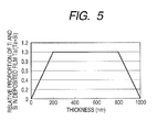
- FIG. 5 is a graph of a composition ratio of a mixed film in the second embodiment.
- FIG. 1 shows a sectional view of a waveplate in a first embodiment.
- the waveplate in the first embodiment is a waveplate including relief-shaped (rugged) gratings formed as a micro-periodic structure on a deposited film 10 composed of a dielectric medium.
- a refractive index of the deposited film 10 is inclined and changes in a film thicknesswise direction. Namely, the deposited film 10 is an inclined film.
- a material gas is introduced onto a dielectric substrate 1 having a refractive index n1, thereby forming a film of a dielectric medium 2 having a refractive index n2 that is approximate to or the same as the refractive index n1 over the surface.
- a material gas is introduced onto the film of the dielectric medium 2 together with the material gas of the dielectric medium 2 while gradually changing flow rates of the two material gases so as to increase step by step a mixture ratio of a dielectric medium 3 having a refractive index n3 larger than the refractive index n1 with respect to the dielectric medium 2.
- a dielectric medium mixed film 4 constructed of the dielectric medium 2 and the dielectric medium 3 is grown on the film of the dielectric medium 2. After a rate of the dielectric medium 3 in the dielectric medium mixed film 4 has reached 100%, a film of the dielectric medium 3 is grown up to an arbitrary film thickness while being kept in a 100% state.
- the material gases of the dielectric medium 3 and a dielectric medium 5 are introduced onto the film of the dielectric medium 3 while gradually changing the flow rates of the material gases of the dielectric medium 3 and the dielectric medium 5 so as to increase step by step the mixture ratio of the dielectric medium 5 having a refractive index smaller than the refractive index n3 of the dielectric medium 3 with respect to the dielectric medium 2.
- a dielectric medium mixed film 6 constructed of the dielectric medium 3 and the dielectric medium 5 is grown on the film of the dielectric medium 3, an upper portion of the mixed film 6 is grown so that the dielectric medium 5 comes to a rate of 100%, and a film of the dielectric medium 5 is grown up to an arbitrary film thickness.
- a deposited film 10 composed of the dielectric medium having the inclined refractive index is obtained.
- the deposited film 10 is formed with relief-shaped gratings 7 as illustrated in FIG. 1 by etching.
- the relief-shaped gratings 7 in the first embodiment can reduce reflection on an interface because of a refractive index difference on the interface with the dielectric substrate 1 being the same or close.
- the refractive index of the dielectric medium 5 on the surface of the deposited film 10 is small, and hence the reflection on the surface can be also decreased.
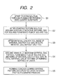
- FIG. 2 is a flowchart of a process in the first embodiment.
- step S1 the dielectric substrate 1 composed of a quartz wafer is disposed in a vacuum container, and Si(OC 2 H 5 ) 4 (which will hereinafter be referred to as TEOS) is introduced as a material gas of a SiO 2 film into the vacuum container. Then, the TEOS defined as the material gas is decomposed and deposited onto the substrate 1 by use of a plasma CVD method, thereby growing the SiO 2 film as a first dielectric medium.
- Si(OC 2 H 5 ) 4 which will hereinafter be referred to as TEOS
- step S2 a dielectric medium mixed film composed of SiO 2 and TiO 2 defined as a material having a higher refractive index than SiO 2 is grown on the SiO 2 film grown in step S1.
- the material gas is introduced in a way that gradually increases a ratio of Ti (I-OC 3 H 7 ) 4 (which will hereinafter be termed TTIP) to the TEOS, thus growing a dielectric mixed film composed of SiO 2 and TiO 2 .
- TTIP Ti-OC 3 H 7
- an element composition ratio of Si and Ti is gradually changed together with the growth of the deposited film defined as the dielectric mixed film by increasing step by step the ratio of the TTIP, thereby enabling a characteristic of the refractive index to be gradually varied.
- step S3 in a state where the ratio of TiO 2 in this dielectric mixed film reaches 100%, a TiO 2 film serving as a second dielectric medium is grown till a predetermined film thickness is reached.
- step S4 the material gas is introduced while gradually increasing a ratio of the TEOS to the TTIP, thereby growing a dielectric mixed film composed of SiO 2 and TiO 2 on the TiO 2 film.
- a deposited film having an inclined refractive index is grown in a way that gradually increases the ratio of SiO 2 , setting the ratio of SiO 2 at 100% as the first dielectric medium on the surface and gradually changing the element composition ratio of the two types of elements such as Si and Ti in the film thicknesswise direction.
- FIG. 3 illustrates a film composition ratio of SiO 2 and TiO 2 .
- the mixed film of TiO 2 and SiO 2 is grown up to a film thickness of 1000 nm while controlling the flow rates of the material gases such as the TEOS and the TTIP.
- the characteristic of the refractive index, which is similarly proportional to the film composition ratio, is obtained.
- step S5 the deposited film of SiO 2 and TiO 2 , which is acquired in step S4, undergoes CF 4 dry etching by a photolithography process.
- This process enables formation of the relief-shaped gratings 7 taking the periodic structure, of which grating pitch is equal to or smaller than a wavelength of an incident light, by patterning with a grating pitch of 0.26 ⁇ m.
- the waveplate in the first embodiment has no difference in the refractive index between the dielectric substrate 1 and the SiO 2 film defined as the first dielectric medium 2 and is therefore capable of reducing the reflection on the dielectric substrate 1 and the reflection on the interface with the relief-shaped gratings 7.
- a fifth dielectric medium 5 constituting the surface of the deposited film 10 is also the SiO 2 film and has a relatively small refractive index, whereby the reflection of the surface of the deposited film 10 can be reduced.
- the average refractive index of the deposited film 10 is, however, high, so that the thickness of the deposited film 10 can be decreased, and the etching of the deposited film 10 is facilitated. Accordingly, the waveplate, which is easy to manufacture, low of cost but ample of productivity and has a high transmittance, is acquired.
- the first embodiment has employed the two types of material gases of Si and Ti and may involve using three or more types of material gasses.
- a phase retardation ⁇ received by the light incident on the relief-shaped gratings 7 is proportional to a groove depth D of the gratings and a magnitude ⁇ n of birefringence.
- a dielectric medium (the same dielectric medium as the dielectric substrate 1) having the same refractive index as that of the dielectric substrate 1 or a dielectric medium having a refractive index approximate to that of the dielectric substrate 1 and a dielectric medium having a refractive index sufficiently larger than that of the dielectric substrate 1, are grown on the dielectric substrate 1 so as to gradually change the element composition ratio.
- the deposited film 10 which is, though high of the refractive index of the whole deposited film 10, small of the refractive index difference on the surface and small of the refractive index difference on the interface with the dielectric substrate, can be grown.
- the waveplate comes to have the small reflectance and the high transmittance because of small refractive index differences between the dielectric substrate and the interface of the deposited film and between the surface of the deposited film and the air.
- the deposited film 10 is the single-layered inclined film having the inclined refractive index and has therefore no reflection on the interface of the film such as a laminated film.
- a construction of the waveplate in the second embodiment is substantially the same as the waveplate in the first embodiment illustrated in FIG. 1 has, and hence its in-depth description is omitted.
- a difference of the waveplate according to the second embodiment from the waveplate according to the first embodiment is such a point that TiO 2 is replaced by Ta 2 O 5 as the dielectric medium.
- FIG. 4 is a flowchart of the process in the second embodiment.
- step S11 the dielectric substrate composed of the quartz wafer is disposed in the vacuum container, and the SiO 2 film starts being grown on this substrate by use of the plasma CVD method.
- the TEOS is used as the material gas for the SiO 2 film in the same way as in the first embodiment.
- step S12 after the start of growing the SiO 2 film, Ta(OC 2 H 5 ) 5 as a material gas of Ta 2 O 5 with an increased refractive index is introduced in a way that increases a ratio of Ta(OC 2 H 5 ) 5 with respect to the TEOS.
- a dielectric mixed film composed of Ta 2 O 5 and SiO 2 is grown while controlling the flow rate of the material gas so as to attain the composition ratio illustrated in FIG. 5 .
- step S13 in a state where the ratio of Ta 2 O 5 becomes 100%, the Ta 2 O 5 film is grown till reaching a predetermined film thickness.
- step S14 the TEOS is introduced while increasing stepwise the ratio of the TEOS with respect to Ta (OC 2 H 5 ) 5 , and a dielectric mixed film composed of SiO 2 and Ta 2 O 5 is grown. Then, the ratio of SiO 2 is made to reach 100% on the surface by increasing stepwise the ratio of SiO 2 , thereby growing the deposited film having the element composition of two types of elements such as Si and Ta and having the refractive index that changes gradually in the thicknesswise direction.
- step S15 the deposited film 10 of Ta 2 O 5 and SiO 2 is subjected to the CF 4 dry etching by the photolithography process, thereby conducting the patterning with the grating pitch of 0.26 ⁇ m and forming the relief-shaped gratings 7 taking the periodic structure, which is equal to or smaller than the wavelength of the incident light.
- the waveplate is formed of the deposited film 10 having the high average refractive index, thereby enabling the grooves of the gratings to be shallowed and facilitating the etching process. Accordingly, the waveplate, which is easy to manufacture, low of the cost but ample of the productivity and has the high transmittance, is acquired.
- the first embodiment and the second embodiment have involved using the material gases each containing atoms such as Ti and Ta and may also involve employing material gases containing atoms such as Nb, Zr, Al and Hf.
- the thus-manufactured phase grating type waveplate can be employed in a measuring apparatus and a variety of optical apparatuses.
- the present invention can be applied to a waveplate that causes phase delay differences such as ⁇ , ⁇ /2 and ⁇ /4 with respect to a wavelength ⁇ of the incident light.
- the design wavelength and the period of the periodic structure can be also changed.
- a waveplate including a dielectric substrate (1) and a periodic structure (7) formed on the dielectric substrate, said periodic structure having a period which is equal to or smaller than a wavelength of an incident light, wherein the periodic structure is constructed of a deposited film (10), and a refractive index of the deposited film gradually changes in a thicknesswise direction of the deposited film.
Landscapes
- Physics & Mathematics (AREA)
- General Physics & Mathematics (AREA)
- Optics & Photonics (AREA)
- Optical Integrated Circuits (AREA)
- Diffracting Gratings Or Hologram Optical Elements (AREA)
- Polarising Elements (AREA)
- Chemical Vapour Deposition (AREA)
Abstract
Description
- The present invention relates to a waveplate such as a 1/4 waveplate, a 1/2 waveplate and a full waveplate (optical waveplate) and to a waveplate manufacturing method.
- A waveplate used for a variety of optical apparatuses has hitherto been manufacturing by polishing a crystal of quartz. The waveplate is adjusted to such a thickness that a phase retardation between an ordinary light and an extraordinary light becomes an (N + 1/4) wavelength in the 1/4 waveplate, an (N + 1/2) wavelength in the 1/2 waveplate and an N wavelength (N is an integer) in the full waveplate.
- Other than these types of waveplates, a waveplate utilizing form birefringence is proposed in (D. C. Flanders, "Submicrometer Periodicity Gratings as Artificial Anisotropic Dielectrics," Applied Physics Letters, vol. 42, pp. 492-494, 15 Mar. 1983.). The waveplate utilizing the form birefringence has gratings (micro-periodic structure) arranged with a smaller period than a wavelength (usage wavelength) of an incident light. The waveplate makes use of a phenomenon that let d be a grating pitch and λ be a usage wavelength, in an area where the grating pitch d is smaller than the wavelength λ, a refractive index np in a direction parallel with the grooves of the gratings is different from a refractive index nc in a direction orthogonal to the grooves of the gratings.
- According to (D. C. Flanders, "Submicrometer Periodicity Gratings as Artificial Anisotropic Dielectrics," Applied Physics Letters, vol. 42, pp. 492-494, 15 Mar. 1983.) given above, when a sectional shape of the grating is rectangular, the refractive indexes np and nc are given by the following equations.


where n1 is a refractive index of amedium 1, n2 is a refractive index of amedium 2, q is an occupying ratio of themedium 1 during one period of the grating, and such a relation is established as 1 ≥ q ≥ 0. - A magnitude Δn of the birefringence is given by the following equation.

- Further, a phase retardation ΔΦ received by the light having the wavelength λ, which gets incident on the gratings with the magnitude Δn of the birefringence, is given by the following equation, where D is a groove depth of the gratings.

From this equation (4), for obtaining a large phase retardation ΔΦ, the groove depth D of the gratings may be increased, or the magnitude Δn of the birefringence may be increased. This relation is established when the section of the gratings takes a sine-wave shape or a triangular-wave shape as well as when the section thereof takes a rectangular shape. - Mainly, the following two methods are given as methods of concretely manufacturing, based on the principle described above, the waveplate utilizing the form birefringence.
- The first manufacturing method is that, at first, a photoresist is formed with the gratings by exposing the photoresist to the light on the basis of an interference exposure method, and a die is manufactured from the gratings. Next, the die is transferred onto a thermosetting resin or a photosetting resin by a hot pressing method or an injection molding method, thus manufacturing the waveplate.
- The second manufacturing method involves, in the same way as by the first manufacturing method, forming the gratings of the photoresist on a dielectric substrate. Next, however, with the photoresist being used as a mask, the dielectric substrate is etched by an ion etching method or a reactive ion etching method, thereby forming the gratings on the surface of the dielectric substrate. The waveplate is thus manufactured.
- In the case of manufacturing this type of gratings by the first manufacturing method, a contact surface area between the medium and an electro-casting die conspicuously increases, and consequently a pull shearing force for exfoliation from the die surface rises. Therefore, the medium hardened when exfoliated is peeled off the dielectric substrate and remains on the die surface, resulting in a problem that the gratings can not be transferred with high accuracy.
- Moreover, the second manufacturing method entails a long period of time for etching, and hence a thickness of a mask for a durable-against-etching photoresist increases, with the result that the mask for the photoresist is hard to form.
- The gratings formed on the photoresist are transferred onto a substance, e.g., chromium, exhibiting high durability against etching, and, in the case of etching with this substance being used as a mask, the following problems arise.
- Namely, if a groove of the grating is deepened, active species, ions and neutral particles, which reach the bottom of the groove, decrease in their numbers, and a progress of the etching is thereby hindered. Then, the gratings taking a desired sectional shape get hard to form.
- This type of problem is caused without depending on the sectional shape of the gratings.
- If the dielectric substrate is large in size, a problem is that intra-surface uniformity based on etching goes under an acceptable level, and a yield declines.
- To cope with these problems,
Japanese Patent Application Laid-Open Publication No. S62-269104 - Further, another known method is that the groove depth is decreased by manufacturing the gratings by using the dielectric medium having the high refractive index as a material. However, in the case of the dielectric medium having the high refractive index, the reflectance rises, and it is difficult to obtain the necessary and sufficient transmittance in terms of the optical element.
- A known method contrived for solving this problem is a method of growing the dielectric medium having the small refractive index on the surface, however, reflection and scattering occur on an interface between the dielectric medium having the high refractive index and the dielectric medium having the low refractive index, and it is hard to acquire the transmittance that is as high as expected.
- It is an illustrative object of the present invention to provide an easy-to-manufacture waveplate capable of solving any one of the problems given above.
- According to one aspect of the present invention, a waveplate comprises a dielectric substrate (1) and a periodic structure (7) formed on the dielectric substrate, said periodic structure having a period which is and equal to or smaller than a wavelength of an incident light, wherein the periodic structure is constructed of a deposited film (10), and a refractive index of the deposited film gradually changes in a thicknesswise direction of the deposited film.
- Further features of the present invention will become apparent from the following description of exemplary embodiments with reference to the attached drawings.
-
FIG. 1 is a sectional view of a waveplate in a first embodiment. -
FIG. 2 is a flowchart of a process in the first embodiment. -
FIG. 3 is a graph of a composition ratio of a mixed film in the first embodiment. -
FIG. 4 is a flowchart of a process in a second embodiment. -
FIG. 5 is a graph of a composition ratio of a mixed film in the second embodiment. - An exemplary embodiment of the present invention will hereinafter be described in detail with reference to the accompanying drawings.
- (First Embodiment)
-
FIG. 1 shows a sectional view of a waveplate in a first embodiment. - The waveplate in the first embodiment is a waveplate including relief-shaped (rugged) gratings formed as a micro-periodic structure on a deposited
film 10 composed of a dielectric medium. A refractive index of the depositedfilm 10 is inclined and changes in a film thicknesswise direction. Namely, the depositedfilm 10 is an inclined film. - Next, a manufacturing method of the waveplate in the first embodiment will be described.
- To begin with, a material gas is introduced onto a
dielectric substrate 1 having a refractive index n1, thereby forming a film of adielectric medium 2 having a refractive index n2 that is approximate to or the same as the refractive index n1 over the surface. - Subsequently, a material gas is introduced onto the film of the
dielectric medium 2 together with the material gas of thedielectric medium 2 while gradually changing flow rates of the two material gases so as to increase step by step a mixture ratio of adielectric medium 3 having a refractive index n3 larger than the refractive index n1 with respect to thedielectric medium 2. - Then, a dielectric medium mixed
film 4 constructed of thedielectric medium 2 and thedielectric medium 3 is grown on the film of thedielectric medium 2. After a rate of thedielectric medium 3 in the dielectric medium mixedfilm 4 has reached 100%, a film of thedielectric medium 3 is grown up to an arbitrary film thickness while being kept in a 100% state. - Further, the material gases of the
dielectric medium 3 and adielectric medium 5 are introduced onto the film of thedielectric medium 3 while gradually changing the flow rates of the material gases of thedielectric medium 3 and thedielectric medium 5 so as to increase step by step the mixture ratio of thedielectric medium 5 having a refractive index smaller than the refractive index n3 of thedielectric medium 3 with respect to thedielectric medium 2. A dielectric medium mixedfilm 6 constructed of thedielectric medium 3 and thedielectric medium 5 is grown on the film of thedielectric medium 3, an upper portion of the mixedfilm 6 is grown so that thedielectric medium 5 comes to a rate of 100%, and a film of thedielectric medium 5 is grown up to an arbitrary film thickness. - Thus, a deposited
film 10 composed of the dielectric medium having the inclined refractive index is obtained. The depositedfilm 10 is formed with relief-shapedgratings 7 as illustrated inFIG. 1 by etching. The relief-shapedgratings 7 in the first embodiment can reduce reflection on an interface because of a refractive index difference on the interface with thedielectric substrate 1 being the same or close. Moreover, the refractive index of thedielectric medium 5 on the surface of the depositedfilm 10 is small, and hence the reflection on the surface can be also decreased. - It is feasible to acquire the waveplate having a high average refractive index and capable of restraining the reflection on the surface and the reflection on the interface with the
dielectric substrate 1. - A specific method of manufacturing the waveplate in the first embodiment will hereinafter be described.
FIG. 2 is a flowchart of a process in the first embodiment. - To start with, in step S1, the
dielectric substrate 1 composed of a quartz wafer is disposed in a vacuum container, and Si(OC2H5)4 (which will hereinafter be referred to as TEOS) is introduced as a material gas of a SiO2 film into the vacuum container. Then, the TEOS defined as the material gas is decomposed and deposited onto thesubstrate 1 by use of a plasma CVD method, thereby growing the SiO2 film as a first dielectric medium. - Subsequently, in step S2, a dielectric medium mixed film composed of SiO2 and TiO2 defined as a material having a higher refractive index than SiO2 is grown on the SiO2 film grown in step S1. The material gas is introduced in a way that gradually increases a ratio of Ti (I-OC3H7)4 (which will hereinafter be termed TTIP) to the TEOS, thus growing a dielectric mixed film composed of SiO2 and TiO2. On this occasion, an element composition ratio of Si and Ti is gradually changed together with the growth of the deposited film defined as the dielectric mixed film by increasing step by step the ratio of the TTIP, thereby enabling a characteristic of the refractive index to be gradually varied.
- In step S3, in a state where the ratio of TiO2 in this dielectric mixed film reaches 100%, a TiO2 film serving as a second dielectric medium is grown till a predetermined film thickness is reached.
- Subsequently, in step S4, the material gas is introduced while gradually increasing a ratio of the TEOS to the TTIP, thereby growing a dielectric mixed film composed of SiO2 and TiO2 on the TiO2 film. A deposited film having an inclined refractive index is grown in a way that gradually increases the ratio of SiO2, setting the ratio of SiO2 at 100% as the first dielectric medium on the surface and gradually changing the element composition ratio of the two types of elements such as Si and Ti in the film thicknesswise direction.
-
FIG. 3 illustrates a film composition ratio of SiO2 and TiO2. The mixed film of TiO2 and SiO2 is grown up to a film thickness of 1000 nm while controlling the flow rates of the material gases such as the TEOS and the TTIP. The characteristic of the refractive index, which is similarly proportional to the film composition ratio, is obtained. - Finally in step S5, the deposited film of SiO2 and TiO2, which is acquired in step S4, undergoes CF4 dry etching by a photolithography process. This process enables formation of the relief-shaped
gratings 7 taking the periodic structure, of which grating pitch is equal to or smaller than a wavelength of an incident light, by patterning with a grating pitch of 0.26 µm. - The waveplate in the first embodiment has no difference in the refractive index between the
dielectric substrate 1 and the SiO2 film defined as thefirst dielectric medium 2 and is therefore capable of reducing the reflection on thedielectric substrate 1 and the reflection on the interface with the relief-shapedgratings 7. Moreover, afifth dielectric medium 5 constituting the surface of the depositedfilm 10 is also the SiO2 film and has a relatively small refractive index, whereby the reflection of the surface of the depositedfilm 10 can be reduced. The average refractive index of the depositedfilm 10 is, however, high, so that the thickness of the depositedfilm 10 can be decreased, and the etching of the depositedfilm 10 is facilitated. Accordingly, the waveplate, which is easy to manufacture, low of cost but ample of productivity and has a high transmittance, is acquired. The first embodiment has employed the two types of material gases of Si and Ti and may involve using three or more types of material gasses. - A phase retardation ΔΦ received by the light incident on the relief-shaped
gratings 7 is proportional to a groove depth D of the gratings and a magnitude Δn of birefringence. Such being the case, as described above, a dielectric medium (the same dielectric medium as the dielectric substrate 1) having the same refractive index as that of thedielectric substrate 1 or a dielectric medium having a refractive index approximate to that of thedielectric substrate 1 and a dielectric medium having a refractive index sufficiently larger than that of thedielectric substrate 1, are grown on thedielectric substrate 1 so as to gradually change the element composition ratio. The depositedfilm 10, which is, though high of the refractive index of the whole depositedfilm 10, small of the refractive index difference on the surface and small of the refractive index difference on the interface with the dielectric substrate, can be grown. - Incidentally, the waveplate comes to have the small reflectance and the high transmittance because of small refractive index differences between the dielectric substrate and the interface of the deposited film and between the surface of the deposited film and the air. Further, the deposited
film 10 is the single-layered inclined film having the inclined refractive index and has therefore no reflection on the interface of the film such as a laminated film. - (Second Embodiment)
- Next, the waveplate according to a second embodiment will be described.
- A construction of the waveplate in the second embodiment is substantially the same as the waveplate in the first embodiment illustrated in
FIG. 1 has, and hence its in-depth description is omitted. A difference of the waveplate according to the second embodiment from the waveplate according to the first embodiment is such a point that TiO2 is replaced by Ta2O5 as the dielectric medium. -
FIG. 4 is a flowchart of the process in the second embodiment. - In the same way as in the first embodiment, to begin with, in step S11, the dielectric substrate composed of the quartz wafer is disposed in the vacuum container, and the SiO2 film starts being grown on this substrate by use of the plasma CVD method. The TEOS is used as the material gas for the SiO2 film in the same way as in the first embodiment.
- In step S12, after the start of growing the SiO2 film, Ta(OC2H5)5 as a material gas of Ta2O5 with an increased refractive index is introduced in a way that increases a ratio of Ta(OC2H5)5 with respect to the TEOS. A dielectric mixed film composed of Ta2O5 and SiO2 is grown while controlling the flow rate of the material gas so as to attain the composition ratio illustrated in
FIG. 5 . In step S13, in a state where the ratio of Ta2O5 becomes 100%, the Ta2O5 film is grown till reaching a predetermined film thickness. - Subsequently in step S14, the TEOS is introduced while increasing stepwise the ratio of the TEOS with respect to Ta (OC2H5)5, and a dielectric mixed film composed of SiO2 and Ta2O5 is grown. Then, the ratio of SiO2 is made to reach 100% on the surface by increasing stepwise the ratio of SiO2, thereby growing the deposited film having the element composition of two types of elements such as Si and Ta and having the refractive index that changes gradually in the thicknesswise direction.
- In step S15, the deposited
film 10 of Ta2O5 and SiO2 is subjected to the CF4 dry etching by the photolithography process, thereby conducting the patterning with the grating pitch of 0.26 µm and forming the relief-shapedgratings 7 taking the periodic structure, which is equal to or smaller than the wavelength of the incident light. - In the second embodiment, similarly to the first embodiment, there is no refractive index difference between the dielectric substrate and the SiO2 film, and therefore the reflection on the interface is small. Further, the surface of the deposited film is also the SiO2 film, and hence the reflection on the surface of the deposited film is comparatively small. The waveplate is formed of the deposited
film 10 having the high average refractive index, thereby enabling the grooves of the gratings to be shallowed and facilitating the etching process. Accordingly, the waveplate, which is easy to manufacture, low of the cost but ample of the productivity and has the high transmittance, is acquired. - The first embodiment and the second embodiment have involved using the material gases each containing atoms such as Ti and Ta and may also involve employing material gases containing atoms such as Nb, Zr, Al and Hf.
- The thus-manufactured phase grating type waveplate can be employed in a measuring apparatus and a variety of optical apparatuses.
- While the present invention has been described with reference to exemplary embodiments, it is to be understood that the invention is not limited to the disclosed exemplary embodiments. The scope of the following claims is to be accorded the broadest interpretation so as to encompass all such modifications and equivalent structures and functions.
- For example, the present invention can be applied to a waveplate that causes phase delay differences such as λ, λ/2 and λ/4 with respect to a wavelength λ of the incident light. Moreover, the design wavelength and the period of the periodic structure can be also changed.
A waveplate including a dielectric substrate (1) and a periodic structure (7) formed on the dielectric substrate, said periodic structure having a period which is equal to or smaller than a wavelength of an incident light, wherein the periodic structure is constructed of a deposited film (10), and a refractive index of the deposited film gradually changes in a thicknesswise direction of the deposited film.
Claims (7)
- A waveplate comprising:a dielectric substrate; anda periodic structure formed on said dielectric substrate, said periodic structure having a period which is equal to or smaller than a wavelength of an incident light,wherein said periodic structure is constructed of a deposited film, and
a refractive index of said deposited film gradually changes in a thicknesswise direction of said deposited film. - A waveplate according to claim 1, wherein an element composition ratio of plural types of elements constituting said deposited film gradually changes in the thicknesswise direction.
- A waveplate according to claim 1, wherein a refractive index of the surface of said deposited film is smaller than a refractive index of a central portion of said deposited film.
- A waveplate according to claim 1, wherein a refractive index of an interface of said deposited film with said dielectric substrate is smaller than the refractive index of the central portion of said deposited film.
- A waveplate manufacturing method comprising:forming a deposited film on a dielectric substrate; andforming a periodic structure having a period which is equal to or smaller than a wavelength of an incident light on said deposited film,wherein said deposited film forming step includes gradually changing an element composition ratio of plural types of elements constituting said deposited film along with growth of said deposited film.
- A waveplate manufacturing method according to claim 5, wherein said deposited film is formed by a plasma CVD method, and
said deposited film forming step includes gradually changing ratios of plural types of material gases along with the growth of said deposited film. - A waveplate manufacturing method according to claim 6, said plural types of material gasses include a gas containing an atom of Si and a gas containing at least one of atoms such as Nb, Ti, Ta, Zr, Al and Hf.
Applications Claiming Priority (1)
| Application Number | Priority Date | Filing Date | Title |
|---|---|---|---|
| JP2006351095A JP2008164680A (en) | 2006-12-27 | 2006-12-27 | Optical wave plate and method for producing the wave plate |
Publications (1)
| Publication Number | Publication Date |
|---|---|
| EP1939654A1 true EP1939654A1 (en) | 2008-07-02 |
Family
ID=39313044
Family Applications (1)
| Application Number | Title | Priority Date | Filing Date |
|---|---|---|---|
| EP07122987A Withdrawn EP1939654A1 (en) | 2006-12-27 | 2007-12-12 | Waveplate utilizing form birefringence and waveplate manufacturing method |
Country Status (3)
| Country | Link |
|---|---|
| US (1) | US8120848B2 (en) |
| EP (1) | EP1939654A1 (en) |
| JP (1) | JP2008164680A (en) |
Cited By (1)
| Publication number | Priority date | Publication date | Assignee | Title |
|---|---|---|---|---|
| CN105745354A (en) * | 2013-11-19 | 2016-07-06 | 旭硝子株式会社 | Thin film formation method, thin film, and glass plate having thin film attached thereto |
Families Citing this family (27)
| Publication number | Priority date | Publication date | Assignee | Title |
|---|---|---|---|---|
| US11726332B2 (en) | 2009-04-27 | 2023-08-15 | Digilens Inc. | Diffractive projection apparatus |
| WO2016020630A2 (en) | 2014-08-08 | 2016-02-11 | Milan Momcilo Popovich | Waveguide laser illuminator incorporating a despeckler |
| EP2842003B1 (en) | 2012-04-25 | 2019-02-27 | Rockwell Collins, Inc. | Holographic wide angle display |
| JP2013227627A (en) * | 2012-04-26 | 2013-11-07 | Kojima Press Industry Co Ltd | Method of manufacturing resin product and resin product |
| US9933684B2 (en) | 2012-11-16 | 2018-04-03 | Rockwell Collins, Inc. | Transparent waveguide display providing upper and lower fields of view having a specific light output aperture configuration |
| CN105612611B (en) | 2013-08-09 | 2019-03-12 | 科磊股份有限公司 | Multi-point illumination for increased detection sensitivity |
| CN105593982B (en) | 2013-08-23 | 2017-10-31 | 科磊股份有限公司 | Wide-band and wide-field angle compensator |
| WO2016042283A1 (en) | 2014-09-19 | 2016-03-24 | Milan Momcilo Popovich | Method and apparatus for generating input images for holographic waveguide displays |
| US10437064B2 (en) | 2015-01-12 | 2019-10-08 | Digilens Inc. | Environmentally isolated waveguide display |
| US9632226B2 (en) | 2015-02-12 | 2017-04-25 | Digilens Inc. | Waveguide grating device |
| WO2017060665A1 (en) | 2015-10-05 | 2017-04-13 | Milan Momcilo Popovich | Waveguide display |
| EP3548939A4 (en) | 2016-12-02 | 2020-11-25 | DigiLens Inc. | WAVE GUIDE DEVICE WITH UNIFORM OUTPUT LIGHTING |
| US10545346B2 (en) | 2017-01-05 | 2020-01-28 | Digilens Inc. | Wearable heads up displays |
| JP7404243B2 (en) | 2018-01-08 | 2023-12-25 | ディジレンズ インコーポレイテッド | Systems and methods for high-throughput recording of holographic gratings in waveguide cells |
| CN114721242B (en) | 2018-01-08 | 2025-08-15 | 迪吉伦斯公司 | Method for manufacturing optical waveguide |
| JP7456929B2 (en) | 2018-01-08 | 2024-03-27 | ディジレンズ インコーポレイテッド | Systems and methods for manufacturing waveguide cells |
| WO2020149956A1 (en) | 2019-01-14 | 2020-07-23 | Digilens Inc. | Holographic waveguide display with light control layer |
| US20200247017A1 (en) | 2019-02-05 | 2020-08-06 | Digilens Inc. | Methods for Compensating for Optical Surface Nonuniformity |
| EP3924759B1 (en) | 2019-02-15 | 2025-07-30 | Digilens Inc. | Methods and apparatuses for providing a holographic waveguide display using integrated gratings |
| US20220283377A1 (en) | 2019-02-15 | 2022-09-08 | Digilens Inc. | Wide Angle Waveguide Display |
| EP3980825A4 (en) | 2019-06-07 | 2023-05-03 | Digilens Inc. | WAVEGUIDES INCORPORATING TRANSPARENT AND REFLECTIVE GRATINGS AND METHODS OF MAKING THEREOF |
| JP2022546413A (en) | 2019-08-29 | 2022-11-04 | ディジレンズ インコーポレイテッド | Vacuum grating and manufacturing method |
| US11662584B2 (en) * | 2019-12-26 | 2023-05-30 | Meta Platforms Technologies, Llc | Gradient refractive index grating for display leakage reduction |
| JP2023534997A (en) * | 2020-07-22 | 2023-08-15 | アプライド マテリアルズ インコーポレイテッド | Method for depositing refractive index films of varying depth |
| WO2022066941A1 (en) * | 2020-09-23 | 2022-03-31 | Applied Materials, Inc. | Fabrication of diffractive optic element having a variable refractive index profile by inkjet printing deposition |
| WO2022150841A1 (en) | 2021-01-07 | 2022-07-14 | Digilens Inc. | Grating structures for color waveguides |
| KR20230153459A (en) | 2021-03-05 | 2023-11-06 | 디지렌즈 인코포레이티드. | Vacuum periodic structure and manufacturing method |
Citations (4)
| Publication number | Priority date | Publication date | Assignee | Title |
|---|---|---|---|---|
| JPS62269104A (en) | 1986-05-16 | 1987-11-21 | Nec Corp | Wavelength plate |
| US5982545A (en) * | 1997-10-17 | 1999-11-09 | Industrial Technology Research Institute | Structure and method for manufacturing surface relief diffractive optical elements |
| US20030156325A1 (en) * | 2001-12-27 | 2003-08-21 | Canon Kabushiki Kaisha | Optical element, optical functional device, polarization conversion device, image display apparatus, and image display system |
| US20050128592A1 (en) * | 2003-01-28 | 2005-06-16 | Nippon Sheet Glass Company, Limited | Optical element, optical circuit provided with the optical element, and method for producing the optical element |
Family Cites Families (3)
| Publication number | Priority date | Publication date | Assignee | Title |
|---|---|---|---|---|
| JP4444693B2 (en) | 2004-02-27 | 2010-03-31 | キヤノン株式会社 | Manufacturing method of optical wave plate |
| US7554734B1 (en) * | 2006-04-28 | 2009-06-30 | Johan Christer Holm | Polarization independent grating |
| US7772768B2 (en) * | 2007-03-02 | 2010-08-10 | Samsung Mobile Display Co., Ltd. | Polarizer and flat panel display apparatus including the same |
-
2006
- 2006-12-27 JP JP2006351095A patent/JP2008164680A/en active Pending
-
2007
- 2007-11-30 US US11/948,343 patent/US8120848B2/en not_active Expired - Fee Related
- 2007-12-12 EP EP07122987A patent/EP1939654A1/en not_active Withdrawn
Patent Citations (4)
| Publication number | Priority date | Publication date | Assignee | Title |
|---|---|---|---|---|
| JPS62269104A (en) | 1986-05-16 | 1987-11-21 | Nec Corp | Wavelength plate |
| US5982545A (en) * | 1997-10-17 | 1999-11-09 | Industrial Technology Research Institute | Structure and method for manufacturing surface relief diffractive optical elements |
| US20030156325A1 (en) * | 2001-12-27 | 2003-08-21 | Canon Kabushiki Kaisha | Optical element, optical functional device, polarization conversion device, image display apparatus, and image display system |
| US20050128592A1 (en) * | 2003-01-28 | 2005-06-16 | Nippon Sheet Glass Company, Limited | Optical element, optical circuit provided with the optical element, and method for producing the optical element |
Non-Patent Citations (1)
| Title |
|---|
| CALLARD S ET AL: "FABRICATION AND CHARACTERIZATION OF GRADED REFRACTIVE INDEX SILICON OXYNITRIDE THIN FILMS", JOURNAL OF VACUUM SCIENCE AND TECHNOLOGY: PART A, AVS /AIP, MELVILLE, NY, US, vol. 15, no. 4, July 1997 (1997-07-01), pages 2088 - 2094, XP001154156, ISSN: 0734-2101 * |
Cited By (2)
| Publication number | Priority date | Publication date | Assignee | Title |
|---|---|---|---|---|
| CN105745354A (en) * | 2013-11-19 | 2016-07-06 | 旭硝子株式会社 | Thin film formation method, thin film, and glass plate having thin film attached thereto |
| CN105745354B (en) * | 2013-11-19 | 2018-03-30 | 旭硝子株式会社 | Film forming method, film and the glass plate with film |
Also Published As
| Publication number | Publication date |
|---|---|
| JP2008164680A (en) | 2008-07-17 |
| US8120848B2 (en) | 2012-02-21 |
| US20080158674A1 (en) | 2008-07-03 |
Similar Documents
| Publication | Publication Date | Title |
|---|---|---|
| EP1939654A1 (en) | Waveplate utilizing form birefringence and waveplate manufacturing method | |
| US8765360B2 (en) | Optical films and methods of making the same | |
| KR102880074B1 (en) | Atomic layer deposition process for fabricating dielectric metasurfaces for wavelengths in the visible spectrum | |
| US12461276B2 (en) | Reflective optical metasurface films | |
| FI128376B (en) | Method of manufacturing a variable efficiency diffractive grating and a diffractive grating | |
| US20080038660A1 (en) | Method Of Making Grating Structures Having High Aspect Ratio | |
| EP2790043B1 (en) | Polarization separation element | |
| EP3631535B1 (en) | Method of manufacturing a height-modulated optical diffractive grating | |
| EP1741003A2 (en) | Optical films and methods of making the same | |
| CN100476464C (en) | Optical films and methods of making the same | |
| US20020122651A1 (en) | Controlling birefringence in an optical waveguide and in an arrayed waveguide grating | |
| US20160370608A1 (en) | Depolarizing plate, optical device and liquid-crystal display device including same, and depolarizing plate production method | |
| EP1569014B1 (en) | Optical retardation plate and method of manufacturing the same | |
| JP4999401B2 (en) | Manufacturing method of optical element having fine irregularities on surface | |
| WO2024253855A1 (en) | Method of fabricating an optical structure | |
| JP3408217B2 (en) | Method for producing fine structure and diffractive optical element | |
| US11885992B1 (en) | Nanofabricated volume gratings | |
| WO2016152771A1 (en) | Grating element | |
| JP2007316270A (en) | Optical component manufacturing method, retardation element, and polarizer | |
| Goh et al. | Deposited poly-Si as on-demand linewidth compensator for on-chip Fabry–Perot interferometer and vertical linear variable optical filter bandpass and passband manipulation | |
| JP2007101856A (en) | Optical retardation element and manufacturing method thereof | |
| Bernet et al. | Nanofabrication and profile tailoring of high index Ta2O5 optical gratings for LiDAR using C4F8/SF6 plasma mixtures | |
| JP2004271828A (en) | Optical element and manufacturing method thereof | |
| Park et al. | Low blaze angle gratings for x-ray and EUV applications | |
| Manner | Fabrication of Metalens-structures Using a Spin-coatable Organic hardmask |
Legal Events
| Date | Code | Title | Description |
|---|---|---|---|
| PUAI | Public reference made under article 153(3) epc to a published international application that has entered the european phase |
Free format text: ORIGINAL CODE: 0009012 |
|
| AK | Designated contracting states |
Kind code of ref document: A1 Designated state(s): AT BE BG CH CY CZ DE DK EE ES FI FR GB GR HU IE IS IT LI LT LU LV MC MT NL PL PT RO SE SI SK TR |
|
| AX | Request for extension of the european patent |
Extension state: AL BA HR MK RS |
|
| 17P | Request for examination filed |
Effective date: 20090105 |
|
| AKX | Designation fees paid |
Designated state(s): DE FR GB IT NL |
|
| 17Q | First examination report despatched |
Effective date: 20090216 |
|
| STAA | Information on the status of an ep patent application or granted ep patent |
Free format text: STATUS: THE APPLICATION HAS BEEN WITHDRAWN |
|
| 18W | Application withdrawn |
Effective date: 20090615 |