EP1936793A1 - Regulated multi-output DC-DC converter - Google Patents
Regulated multi-output DC-DC converter Download PDFInfo
- Publication number
- EP1936793A1 EP1936793A1 EP07254481A EP07254481A EP1936793A1 EP 1936793 A1 EP1936793 A1 EP 1936793A1 EP 07254481 A EP07254481 A EP 07254481A EP 07254481 A EP07254481 A EP 07254481A EP 1936793 A1 EP1936793 A1 EP 1936793A1
- Authority
- EP
- European Patent Office
- Prior art keywords
- power converter
- voltage
- output
- coupled
- energy transfer
- Prior art date
- Legal status (The legal status is an assumption and is not a legal conclusion. Google has not performed a legal analysis and makes no representation as to the accuracy of the status listed.)
- Withdrawn
Links
- 230000001105 regulatory effect Effects 0.000 title abstract description 11
- 230000007423 decrease Effects 0.000 claims description 14
- 239000003990 capacitor Substances 0.000 claims description 12
- 230000001419 dependent effect Effects 0.000 claims 2
- 230000003247 decreasing effect Effects 0.000 abstract description 2
- 238000000034 method Methods 0.000 description 10
- 230000033228 biological regulation Effects 0.000 description 7
- 238000010586 diagram Methods 0.000 description 2
- 238000002955 isolation Methods 0.000 description 2
- 238000006243 chemical reaction Methods 0.000 description 1
- 230000010354 integration Effects 0.000 description 1
- 229910044991 metal oxide Inorganic materials 0.000 description 1
- 150000004706 metal oxides Chemical class 0.000 description 1
- 238000012986 modification Methods 0.000 description 1
- 230000004048 modification Effects 0.000 description 1
- 239000004065 semiconductor Substances 0.000 description 1
Images




Classifications
-
- H—ELECTRICITY
- H02—GENERATION; CONVERSION OR DISTRIBUTION OF ELECTRIC POWER
- H02M—APPARATUS FOR CONVERSION BETWEEN AC AND AC, BETWEEN AC AND DC, OR BETWEEN DC AND DC, AND FOR USE WITH MAINS OR SIMILAR POWER SUPPLY SYSTEMS; CONVERSION OF DC OR AC INPUT POWER INTO SURGE OUTPUT POWER; CONTROL OR REGULATION THEREOF
- H02M3/00—Conversion of DC power input into DC power output
- H02M3/02—Conversion of DC power input into DC power output without intermediate conversion into AC
- H02M3/04—Conversion of DC power input into DC power output without intermediate conversion into AC by static converters
- H02M3/10—Conversion of DC power input into DC power output without intermediate conversion into AC by static converters using discharge tubes with control electrode or semiconductor devices with control electrode
- H02M3/145—Conversion of DC power input into DC power output without intermediate conversion into AC by static converters using discharge tubes with control electrode or semiconductor devices with control electrode using devices of a triode or transistor type requiring continuous application of a control signal
- H02M3/155—Conversion of DC power input into DC power output without intermediate conversion into AC by static converters using discharge tubes with control electrode or semiconductor devices with control electrode using devices of a triode or transistor type requiring continuous application of a control signal using semiconductor devices only
- H02M3/156—Conversion of DC power input into DC power output without intermediate conversion into AC by static converters using discharge tubes with control electrode or semiconductor devices with control electrode using devices of a triode or transistor type requiring continuous application of a control signal using semiconductor devices only with automatic control of output voltage or current, e.g. switching regulators
- H02M3/158—Conversion of DC power input into DC power output without intermediate conversion into AC by static converters using discharge tubes with control electrode or semiconductor devices with control electrode using devices of a triode or transistor type requiring continuous application of a control signal using semiconductor devices only with automatic control of output voltage or current, e.g. switching regulators including plural semiconductor devices as final control devices for a single load
- H02M3/1588—Conversion of DC power input into DC power output without intermediate conversion into AC by static converters using discharge tubes with control electrode or semiconductor devices with control electrode using devices of a triode or transistor type requiring continuous application of a control signal using semiconductor devices only with automatic control of output voltage or current, e.g. switching regulators including plural semiconductor devices as final control devices for a single load comprising at least one synchronous rectifier element
-
- H—ELECTRICITY
- H02—GENERATION; CONVERSION OR DISTRIBUTION OF ELECTRIC POWER
- H02M—APPARATUS FOR CONVERSION BETWEEN AC AND AC, BETWEEN AC AND DC, OR BETWEEN DC AND DC, AND FOR USE WITH MAINS OR SIMILAR POWER SUPPLY SYSTEMS; CONVERSION OF DC OR AC INPUT POWER INTO SURGE OUTPUT POWER; CONTROL OR REGULATION THEREOF
- H02M3/00—Conversion of DC power input into DC power output
- H02M3/02—Conversion of DC power input into DC power output without intermediate conversion into AC
- H02M3/04—Conversion of DC power input into DC power output without intermediate conversion into AC by static converters
- H02M3/10—Conversion of DC power input into DC power output without intermediate conversion into AC by static converters using discharge tubes with control electrode or semiconductor devices with control electrode
- H02M3/145—Conversion of DC power input into DC power output without intermediate conversion into AC by static converters using discharge tubes with control electrode or semiconductor devices with control electrode using devices of a triode or transistor type requiring continuous application of a control signal
- H02M3/155—Conversion of DC power input into DC power output without intermediate conversion into AC by static converters using discharge tubes with control electrode or semiconductor devices with control electrode using devices of a triode or transistor type requiring continuous application of a control signal using semiconductor devices only
- H02M3/156—Conversion of DC power input into DC power output without intermediate conversion into AC by static converters using discharge tubes with control electrode or semiconductor devices with control electrode using devices of a triode or transistor type requiring continuous application of a control signal using semiconductor devices only with automatic control of output voltage or current, e.g. switching regulators
- H02M3/158—Conversion of DC power input into DC power output without intermediate conversion into AC by static converters using discharge tubes with control electrode or semiconductor devices with control electrode using devices of a triode or transistor type requiring continuous application of a control signal using semiconductor devices only with automatic control of output voltage or current, e.g. switching regulators including plural semiconductor devices as final control devices for a single load
-
- H—ELECTRICITY
- H02—GENERATION; CONVERSION OR DISTRIBUTION OF ELECTRIC POWER
- H02M—APPARATUS FOR CONVERSION BETWEEN AC AND AC, BETWEEN AC AND DC, OR BETWEEN DC AND DC, AND FOR USE WITH MAINS OR SIMILAR POWER SUPPLY SYSTEMS; CONVERSION OF DC OR AC INPUT POWER INTO SURGE OUTPUT POWER; CONTROL OR REGULATION THEREOF
- H02M1/00—Details of apparatus for conversion
- H02M1/0045—Converters combining the concepts of switch-mode regulation and linear regulation, e.g. linear pre-regulator to switching converter, linear and switching converter in parallel, same converter or same transistor operating either in linear or switching mode
-
- H—ELECTRICITY
- H02—GENERATION; CONVERSION OR DISTRIBUTION OF ELECTRIC POWER
- H02M—APPARATUS FOR CONVERSION BETWEEN AC AND AC, BETWEEN AC AND DC, OR BETWEEN DC AND DC, AND FOR USE WITH MAINS OR SIMILAR POWER SUPPLY SYSTEMS; CONVERSION OF DC OR AC INPUT POWER INTO SURGE OUTPUT POWER; CONTROL OR REGULATION THEREOF
- H02M1/00—Details of apparatus for conversion
- H02M1/0083—Converters characterised by their input or output configuration
- H02M1/009—Converters characterised by their input or output configuration having two or more independently controlled outputs
-
- Y—GENERAL TAGGING OF NEW TECHNOLOGICAL DEVELOPMENTS; GENERAL TAGGING OF CROSS-SECTIONAL TECHNOLOGIES SPANNING OVER SEVERAL SECTIONS OF THE IPC; TECHNICAL SUBJECTS COVERED BY FORMER USPC CROSS-REFERENCE ART COLLECTIONS [XRACs] AND DIGESTS
- Y02—TECHNOLOGIES OR APPLICATIONS FOR MITIGATION OR ADAPTATION AGAINST CLIMATE CHANGE
- Y02B—CLIMATE CHANGE MITIGATION TECHNOLOGIES RELATED TO BUILDINGS, e.g. HOUSING, HOUSE APPLIANCES OR RELATED END-USER APPLICATIONS
- Y02B70/00—Technologies for an efficient end-user side electric power management and consumption
- Y02B70/10—Technologies improving the efficiency by using switched-mode power supplies [SMPS], i.e. efficient power electronics conversion e.g. power factor correction or reduction of losses in power supplies or efficient standby modes
Definitions
- the present invention relates generally to electronic circuits, and more specifically, the invention relates to circuits in which there is power regulation.
- a first aspect of the invention provides a power converter, comprising:
- FIG. 1 is a schematic that shows generally an example functional block diagram of a power converter or switching regulator with a positive and a negative output referenced to an input return in accordance with the teachings of the present invention.
- FIG. 2 is a schematic that shows generally a power converter including an example shunt regulator that regulates output voltages in accordance with the teachings of the present invention.
- FIG. 3 is a schematic that shows generally a power converter that includes an alternative example shunt regulator that regulates output voltages in accordance with the teachings of the present invention.
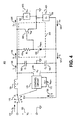
- FIG. 4 is a schematic that shows generally a power converter that includes an example shunt regulator circuit that regulates a desired output voltage in accordance with the teachings of the present invention.
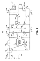
- FIG. 5 is a schematic that shows generally a power converter that includes an example temperature compensated shunt regulator circuit that regulates a desired output voltage in accordance with the teachings of the present invention.
- FIG. 6 is a schematic that shows generally a power converter that includes an alternative example temperature compensated shunt regulator circuit that regulates a desired output voltage in accordance with the teachings of the present invention.
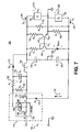
- FIG. 7 is a schematic that shows generally an example power converter in greater detail in accordance with the teachings of the present invention.
- FIG. 8 is a schematic that shows generally an alternative example power converter circuit in accordance with the teachings of the present invention.
- some example power supply regulators in accordance with the teachings of the present invention utilize switched mode power conversion that provide two output voltages of opposite polarity with respect to a common reference that is the input return.
- Examples of the disclosed power supply regulators may be used in a variety of applications in which positive and negative direct current (DC) output voltages are provided from a higher input voltage without an isolation transformer.
- the example methods disclosed can provide two regulated output voltages at lower costs and higher efficiency than other known methods. More flexibility is provided by the disclosed power supply regulators and methods in the selection of output voltages than by other known methods that require high currents to flow in Zener diodes to set output voltages.
- Some target applications for the disclosed power supply regulator and methods are those that do not require galvanic isolation between input and output, such as power supplies for major household appliances.
- FIG. 1 is a functional block diagram that shows an example generalized power converter or switching regulator 100 in accordance with the teachings of the present invention with a positive and a negative output 160 and 165, respectively, referenced to the input return.
- a DC input voltage V G 105 is coupled to switch S 1 115, which is controlled by control circuit 170.
- control circuit 170 includes circuitry to employ any of a variety of switching techniques including at least one of a constant frequency pulse width modulation (PWM), variable frequency PWM, on/off control or the like.
- PWM pulse width modulation
- Control circuit 170 also uses a reference voltage V REF1 175 for the purpose of regulating an output.
- An energy transfer element which is illustrated as inductor L 1 125, is coupled between switch S 1 115 and the outputs of the regulator circuit 100.
- the outputs are shown as output voltage V 1 160 across load impedance Z 1 150 and output voltage V 2 165 across load impedance Z 2 155.
- Capacitor C 1 140 is illustrated as being coupled across load impedance Z 1 150 and capacitor C 2 145 is illustrated as being coupled across load impedance Z 2 155.
- the outputs are each coupled to a ground terminal coupled to both load impedance Z 1 150 and load impedance Z 2 155.
- DC input voltage V G 105 is converted to output voltage V 1 160 across load impedance Z 1 150 and output voltage V 2 165 across load impedance Z 2 155 by the action or switching of switch S 1 115 in response to a control circuit 170.
- switch S1 115 is illustrated in FIG. 1 as a single pole, multi-throw switch adapted to switch among three positions or settings. It is appreciated that switch S1 115 may be implemented using a variety of techniques such as for example using a circuit to provide the described switching function, or the like.
- switch S1 115 includes a terminal coupled to inductor 125 and can be coupled to be set in a first setting or position G to provide a conduction path for inductor 125 to receive current I G 110, or in a second setting or position F to provide a conduction path for inductor 125 to receive current I F 120, or in a third or off setting or position X, such that inductor 125 is not coupled to receive either current I G 110 or current I F 120.
- switch S 1 115 when switch S 1 115 is in position G, the current I L 130 in inductor L 1 125 is the same as the input current I G 110 supplied from the input voltage V G 105.
- control circuit 170 switches switch S 1 115 between positions G, X, and F with sequence and durations to regulate one output according to the value of the reference voltage V RF1 175.
- the switch S 1 115 spends no time at position X.
- the single regulated output may be V 1 160, V 2 165, or a combination of both.
- a shunt circuit 180 that is coupled across an output of power converter 100 uses another reference voltage V REF2 185. The shunt circuit 180 may increase or decrease current I 1 135 or current I 2 137 to regulate one additional output.
- switch S 1 115 produces currents I L 130, I G 110, and I F 120 that contain triangular or trapezoidal components.
- Capacitors C1 140 and C2 145 filter currents I L 130 and I F 120 respectively, which produce the respective DC output voltages V 1 160 and V 2 165 that have small alternating current (AC) variations relative to their DC values.
- Load impedances Z 1 150 and Z 2 155 with shunt circuit 180 produce currents I 1 135 and I 2 137 from the respective output voltages V 1 160 and V 2 165.
- switch S 1 115 may be controlled to regulate only a single output voltage because controller 170 has only one reference voltage V RF1 170. Without further means of regulation, the other output voltage will change with currents I 1 135 and I 2 137 that are responsive to changes in load impedances Z 1 160 and Z 2 165. To regulate more than one output voltage requires another regulator to change current I 1 135 or I 2 137 in response to changes in output voltages V 1 160 and V 2 165.
- control circuit 170 is shown having three inputs including an input coupled to an end of load impedance Z 1 150, an input coupled to an end of load impedance Z 2 155, and an input coupled to a ground terminal.
- control circuit 170 is not included or is instead adapted to switch switch S 1 115 in a fixed pattern, which produces an unregulated output voltage V 1 160 or V 2 165.
- current I L 130 through inductor L 1 125 increases when the voltage across inductor L 1 125 is the difference between the input voltage V G 105 and output voltage V 1 160, which is what occurs when switch S 1 115 is in position G.
- the current I L 130 through inductor L 1 125 decreases when the voltage across inductor L 1 125 is the sum of output voltage V 1 160 and output voltage V 2 165, which is what occurs when switch S 1 115 is in position F.
- FIG. 2 shows generally a power converter or power supply regulator 200, which includes a shunt regulator 205 coupled to regulate an output voltage V 2 165 by adding more or less current to the load current I Z1 235 from load impedance Z 1 150 in response to the output voltage V 2 165 on load impedance Z 2 155.
- shunt regulator 205 changes current I 1 135 independently in response to changes in output currents I Z1 235 and I Z2 240 to regulate the desired output voltage V 2 165 in accordance with the teachings of the present invention.
- Output currents I Z1 235 and I Z2 240 may change in response to changes in the respective load impedances Z 1 and Z 2 , or in response to a change in the input voltage V G 105.
- shunt regulator 205 only adds to the current in the load Z 1 150 if the load impedance Z 1 150 is insufficient to regulate the desired output voltage V 2 165.
- power supply regulator 200 includes power supply regulator 100 of FIG. 1 with the addition of shunt regulator 205 to perform the function of shunt circuit 180 with reference voltage V REF2 185.
- control circuit 170 switches switch S 1 115 to regulate an output voltage V O 245, which is the sum of V 1 160 and V 2 165.
- shunt regulator 205 includes a transconductance amplifier 225 that produces unidirectional current from current source I SH1 250 coupled across load impedance Z 1 150 to regulate voltage V 2 165 across load impedance Z 2 155. Since the controller 170 regulates the sum of V1 160 and V2 165, regulation of V 2 165 by shunt regulator 205 also regulates V 1 160. In operation, if there is a change in load to cause a decrease in current I Z2 240, the control circuit 170 will modify the switching of switch S 1 to regulate the value of output voltage V O 245 in accordance with the teachings of the present invention.
- current source I SH1 250 will decrease to maintain output voltages V 1 160 and V 2 165 at the values determined by the reference voltage V REF2 185. If there is a change in load impedance Z 1 160 to cause a decrease in current I Z1 235, the current source I SH1 250 will increase in response to a decrease in output voltage V 2 165 to regulate the output voltages V 1 160 and V 2 165.
- shunt regulator 205 is included in an integrated circuit.
- FIG. 3 shows generally a power converter or power supply regulator 300, which includes a shunt regulator 305 coupled to regulate an output voltage V 1 160 by adding more or less current to the load current I Z2 240 from load impedance Z 2 150 in response to the output voltage V 1 160 on load impedance Z 1 150.
- shunt regulator 305 changes current I 2 137 independently in response to changes in output currents I Z1 235 and I Z2 240 to regulate the desired output voltage V 1 160 in accordance with the teachings of the present invention.
- Output currents Izi 235 and I Z2 240 may change in response to changes in the respective load impedances Z 1 and Z 2 , or in response to a change in the input voltage V G 105.
- shunt regulator 305 only adds to the current in the load Z 2 155 if the load impedance Z 2 150 is insufficient to regulate the desired output voltage V 1 160.
- power supply 300 includes power supply regulator 100 of FIG. 1 with the addition of shunt regulator 305 with voltage reference V REF3 320 to perform the function of shunt circuit 180 with reference voltage V REF2 185.
- control circuit 170 switches switch S 1 115 to regulate an output voltage V O 245, which is the sum of V 1 160 and V 2 165.
- transconductance amplifier 325 included in shunt regulator 305 produces unidirectional current from current source I SH2 350 coupled across load impedance Z 2 155 to regulate voltage V 1 160 across load impedance Z 1 150. Since the controller 170 regulates the sum of V 1 160 and V 2 165, regulation of V 1 160 by shunt regulator 305 also regulates V 2 165. In operation, if there is a change in load to cause a decrease in current I Z1 235, the control circuit 170 will modify the switching of switch S 1 to regulate the value of output voltage V O 245 in accordance with the teachings of the present invention.
- current source I SH2 350 will decrease to maintain output voltages V 1 160 and V 2 165 at the values determined by the reference voltage V REF3 320. If there is a change in load impedance Z 2 165 to cause a decrease in current I Z2 240, the current source I SH2 350 will increase in response to a decrease in output voltage V 1 160 to regulate the output voltages V 1 160 and V 2 165.
- shunt regulator 305 is included in an integrated circuit.
- the shunt regulator 205 or 305 should regulate the output voltage that requires the tighter regulation.
- the example of FIG. 2 is preferable when the voltage V 2 165 requires tighter regulation than the voltage V 1 160
- the example of FIG. 3 is preferable when the voltage V 1 160 requires tighter regulation than the voltage V 2 165.
- FIG. 4 shows generally a power converter or power supply regulator 400, with one example of shunt regulator 205 that uses a resistor R 1 415, a Zener diode 420, and an NPN transistor 405.
- Zener diode 420 sets a reference voltage V REF2 at the base of the NPN transistor 405.
- Resistor R1 415 provides current to the Zener diode 420 and to the base of the NPN transistor 405.
- the voltage V O2 425 is regulated to be the voltage V REF2 reduced by the base to emitter voltage V BE of NPN transistor 405. Since the base to emitter voltage changes with temperature, output voltages V O1 410 and V O2 425 will also change with temperature.
- FIG. 5 shows generally a power converter or power supply regulator 500, with another example of shunt regulator 205 that adds an NPN transistor 550 to the example circuit of FIG. 4 .
- the base to emitter voltage of transistor 550 is substantially equal to the base to emitter voltage of transistor 405 at all temperatures. Therefore, the output voltage V O2 425 in the example of FIG. 5 is regulated to be the voltage V REF2 from Zener diode 420, substantially invariant to changes in temperature. It is preferable for the NPN transistors 405 and 550 to be identical for the best temperature compensation.
- FIG. 6 shows generally a power converter or power supply regulator 600 that combines the example of the shunt regulator 305 of FIG. 3 with the temperature compensating technique of FIG. 5 .
- Zener diode 620 establishes the reference voltage V REF3 with current through a resistor R 2 615 and PNP transistor 650.
- Another PNP transistor 605 performs the function of current source I SH2 350 of FIG. 3 . It is preferable for the PNP transistors 605 and 650 to be identical for the best temperature compensation.
- bipolar transistors 405, 550, 605, and 650 are illustrated as including single transistors.
- teachings of the present invention are not limited to single transistors and that additional transistors or other circuit elements may be added to bipolar transistors 405, 550, 605, and 650 as appropriate such as for example Darlington transistor pairs or the like to realize the desired circuit performance in accordance with the teachings of the present invention.
- FIG. 7 is one example schematic showing generally the power converter or regulator circuit of FIG. 5 with increased detail and optional components.
- switch S 1 115 including a diode D 1 710 and a transistor 745.
- Transistor 745 is included in an integrated circuit 705 with a control circuit 740 and a reference voltage V REF1 that is not shown to avoid obscuring the illustration with unnecessary detail.
- integrated circuit 705 may be a LNK304 produced by Power Integrations, Inc. of San Jose, CA.
- integrated circuit 705 is coupled between the DC input voltage V G 105 and the inductor L 1 125.
- capacitor C 4 735 is a bypass capacitor coupled to the BP terminal of integrated circuit 705 for the operation of integrated circuit 705.
- control circuit 740 receives a signal proportional to the output voltage V O that is on capacitor C 3 730.
- Capacitor C 3 charges to approximately the sum of output voltages V O1 410 and V O2 425 when diode D 1 710 in switch 115 conducts the freewheeling current I F 120.
- diode D 1 710 automatically configures the switch S 1 115 to position F when the diode D 1 710 is conducting and to position G or X when the diode D 1 710 is not conducting.
- Optional resistor R 5 750 reduces the power dissipation in NPN transistor 405, and also limits the current in NPN transistor 405.
- Resistors R 6 755 and R 7 760 provide minimum loading to the outputs should the load impedances Z 1 150 and Z 2 155 be removed.
- FIG. 8 is another example schematic showing generally the power converter or regulator circuit of FIG. 7 with a single capacitor C 5 810 coupled across the outputs replacing the previously described two capacitors C 1 140 and C 2 145 to reduce the cost of the power supply.
Landscapes
- Engineering & Computer Science (AREA)
- Power Engineering (AREA)
- Dc-Dc Converters (AREA)
- Inverter Devices (AREA)
Abstract
Description
- The present invention relates generally to electronic circuits, and more specifically, the invention relates to circuits in which there is power regulation.
- Electrical devices need power to operate. Many electrical devices are powered using switched mode power converters. Some switched mode power converters are designed to provide multiple output voltages. One challenge with power converters of this type is to provide positive and negative DC output voltages. Known power converters of this type often rely on fixed values of Zener diodes to set the output voltages. In many such circuits, the Zener diodes conduct a substantial portion if not all the current in one of the loads. The power lost in the Zener diodes in these known circuits results in low efficiency that is unacceptable in many applications.
The present invention seeks to overcome or ameliorate at least one problem associated with the prior art, or provide a useful alternative thereto.
A first aspect of the invention provides a power converter, comprising: - an energy transfer element coupled between a power converter input and first and second power converter outputs;
- a switch coupled between the power converter input and the energy transfer element; and
- a control circuit coupled to the switch to control switching of the switch to generate a first output voltage at the first power converter output and a second output voltage at the second power converter output, wherein a sum of the first and second output voltages is regulated in response to a first voltage reference, wherein the second output voltage is regulated in response to a second voltage reference, wherein a current in the energy transfer element is coupled to be increased when a voltage across the energy transfer element is a difference between an input voltage at the power converter input and the first output voltage, and wherein the current in the energy transfer element is coupled to be decreased when the voltage across the energy transfer element is the sum of the first and second output voltages.
- an energy transfer element coupled between a power converter input and first and second power converter outputs;
- a switch coupled between the power converter input and the energy transfer element;
- a control circuit coupled to the switch to control switching of the switch to generate a first output voltage at the first power converter output and a second output voltage at the second power converter output, wherein the first output voltage is regulated in response to a voltage reference, wherein a current in the energy transfer element is coupled to increase when a voltage across the energy transfer element is a difference between an input voltage at the power converter input and the first output voltage, wherein the current in the energy transfer element is coupled to decrease when the voltage across the energy transfer element is a sum of the first and second output voltages; and
- a shunt circuit coupled across the second power converter output to regulate the first output voltage at the first power converter output in response to the voltage reference.
- Non-limiting and non-exhaustive embodiments of the present invention are described with reference to the following figures, wherein like reference numerals refer to like parts throughout the various views unless otherwise specified.
-
FIG. 1 is a schematic that shows generally an example functional block diagram of a power converter or switching regulator with a positive and a negative output referenced to an input return in accordance with the teachings of the present invention. -
FIG. 2 is a schematic that shows generally a power converter including an example shunt regulator that regulates output voltages in accordance with the teachings of the present invention. -
FIG. 3 is a schematic that shows generally a power converter that includes an alternative example shunt regulator that regulates output voltages in accordance with the teachings of the present invention. -
FIG. 4 is a schematic that shows generally a power converter that includes an example shunt regulator circuit that regulates a desired output voltage in accordance with the teachings of the present invention. -
FIG. 5 is a schematic that shows generally a power converter that includes an example temperature compensated shunt regulator circuit that regulates a desired output voltage in accordance with the teachings of the present invention. -
FIG. 6 is a schematic that shows generally a power converter that includes an alternative example temperature compensated shunt regulator circuit that regulates a desired output voltage in accordance with the teachings of the present invention. -
FIG. 7 is a schematic that shows generally an example power converter in greater detail in accordance with the teachings of the present invention. -
FIG. 8 is a schematic that shows generally an alternative example power converter circuit in accordance with the teachings of the present invention. - Examples related to power supply regulators are disclosed. In the following description, numerous specific details are set forth in order to provide a thorough understanding of the present invention. It will be apparent, however, to one having ordinary skill in the art that the specific detail need not be employed to practice the present invention. Well-known methods related to the implementation have not been described in detail in order to avoid obscuring the present invention.
- Reference throughout this specification to "one embodiment," "an embodiment," "one example" or "an example" means that a particular feature, structure or characteristic described in connection with the embodiment is included in at least one embodiment or example of the present invention. Thus, the appearances of the phrases "in one embodiment," "in an embodiment," "in one example" or "in an example" in various places throughout this specification are not necessarily all referring to the same embodiment. Furthermore, the particular features, structures or characteristics may be combined for example into any suitable combinations and/or sub-combinations in one or more embodiments or examples.
- As will be discussed, some example power supply regulators in accordance with the teachings of the present invention utilize switched mode power conversion that provide two output voltages of opposite polarity with respect to a common reference that is the input return. Examples of the disclosed power supply regulators may be used in a variety of applications in which positive and negative direct current (DC) output voltages are provided from a higher input voltage without an isolation transformer. The example methods disclosed can provide two regulated output voltages at lower costs and higher efficiency than other known methods. More flexibility is provided by the disclosed power supply regulators and methods in the selection of output voltages than by other known methods that require high currents to flow in Zener diodes to set output voltages. Some target applications for the disclosed power supply regulator and methods are those that do not require galvanic isolation between input and output, such as power supplies for major household appliances.
- To illustrate,
FIG. 1 is a functional block diagram that shows an example generalized power converter or switchingregulator 100 in accordance with the teachings of the present invention with a positive and anegative output 160 and 165, respectively, referenced to the input return. As shown, a DCinput voltage V G 105 is coupled to switchS 1 115, which is controlled bycontrol circuit 170. In the various examples,control circuit 170 includes circuitry to employ any of a variety of switching techniques including at least one of a constant frequency pulse width modulation (PWM), variable frequency PWM, on/off control or the like.Control circuit 170 also uses areference voltage V REF1 175 for the purpose of regulating an output. An energy transfer element, which is illustrated asinductor L 1 125, is coupled betweenswitch S 1 115 and the outputs of theregulator circuit 100. In the illustrated example, the outputs are shown asoutput voltage V 1 160 acrossload impedance Z 1 150 and output voltage V2 165 acrossload impedance Z 2 155. Capacitor C1 140 is illustrated as being coupled acrossload impedance Z 1 150 and capacitor C2 145 is illustrated as being coupled across load impedance Z2 155. As shown in the illustrated example ofFIG. 1 , the outputs are each coupled to a ground terminal coupled to bothload impedance Z 1 150 and load impedance Z2 155. - In operation, DC
input voltage V G 105 is converted tooutput voltage V 1 160 acrossload impedance Z 1 150 and output voltage V2 165 acrossload impedance Z 2 155 by the action or switching ofswitch S 1 115 in response to acontrol circuit 170. For explanation purposes,switch S1 115 is illustrated inFIG. 1 as a single pole, multi-throw switch adapted to switch among three positions or settings. It is appreciated thatswitch S1 115 may be implemented using a variety of techniques such as for example using a circuit to provide the described switching function, or the like. - As shown in the example,
switch S1 115 includes a terminal coupled toinductor 125 and can be coupled to be set in a first setting or position G to provide a conduction path forinductor 125 to receivecurrent I G 110, or in a second setting or position F to provide a conduction path forinductor 125 to receivecurrent I F 120, or in a third or off setting or position X, such thatinductor 125 is not coupled to receive eithercurrent I G 110 orcurrent I F 120. Thus, whenswitch S 1 115 is in position G, thecurrent I L 130 ininductor L 1 125 is the same as theinput current I G 110 supplied from theinput voltage V G 105. Whenswitch S 1 115 is in position F, thecurrent I L 130 ininductor L 1 125 is the same asfreewheeling current I F 120 derived from an output of the power converter as shown. Whenswitch S 1 115 is in position X, thecurrent I L 130 ininductor L 1 125 is zero. - In the illustrated example,
control circuit 170switches switch S 1 115 between positions G, X, and F with sequence and durations to regulate one output according to the value of thereference voltage V RF1 175. In one mode of operation, (continuous conduction mode) theswitch S 1 115 spends no time at position X. The single regulated output may beV 1 160, V2 165, or a combination of both. Ashunt circuit 180 that is coupled across an output ofpower converter 100 uses anotherreference voltage V REF2 185. Theshunt circuit 180 may increase or decreasecurrent I 1 135 orcurrent I 2 137 to regulate one additional output. - In operation, the switching of
switch S 1 115 produces currents IL 130, IG 110, and IF 120 that contain triangular or trapezoidal components.Capacitors C1 140 andC2 145 filter currents IL 130 andI F 120 respectively, which produce the respective DCoutput voltages V 1 160 and V2 165 that have small alternating current (AC) variations relative to their DC values.Load impedances Z 1 150 andZ 2 155 withshunt circuit 180 produce currents I1 135 and I2 137 from the respectiveoutput voltages V 1 160 and V2 165. - For the regulator of
FIG. 1 , switchS 1 115 may be controlled to regulate only a single output voltage becausecontroller 170 has only onereference voltage V RF1 170. Without further means of regulation, the other output voltage will change with currents I1 135 and I2 137 that are responsive to changes inload impedances Z 1 160 and Z2 165. To regulate more than one output voltage requires another regulator to change current I1 135 or I2 137 in response to changes inoutput voltages V 1 160 and V2 165. In the illustrated example,control circuit 170 is shown having three inputs including an input coupled to an end ofload impedance Z 1 150, an input coupled to an end ofload impedance Z 2 155, and an input coupled to a ground terminal. - In one example of the power converter or
power supply regulator 100,control circuit 170 is not included or is instead adapted to switchswitch S 1 115 in a fixed pattern, which produces an unregulatedoutput voltage V 1 160 or V2 165. In this example, current IL 130 throughinductor L 1 125 increases when the voltage acrossinductor L 1 125 is the difference between theinput voltage V G 105 andoutput voltage V 1 160, which is what occurs whenswitch S 1 115 is in position G. Continuing with this example, the current IL 130 throughinductor L 1 125 decreases when the voltage acrossinductor L 1 125 is the sum ofoutput voltage V 1 160 and output voltage V2 165, which is what occurs whenswitch S 1 115 is in position F. -
FIG. 2 shows generally a power converter orpower supply regulator 200, which includes ashunt regulator 205 coupled to regulate an output voltage V2 165 by adding more or less current to the load current IZ1 235 fromload impedance Z 1 150 in response to the output voltage V2 165 onload impedance Z 2 155. In the illustrated example,shunt regulator 205 changes current I1 135 independently in response to changes in output currents IZ1 235 and IZ2 240 to regulate the desired output voltage V2 165 in accordance with the teachings of the present invention. Output currents IZ1 235 and IZ2 240 may change in response to changes in the respective load impedances Z1 and Z2, or in response to a change in theinput voltage V G 105. In operation,shunt regulator 205 only adds to the current in theload Z 1 150 if theload impedance Z 1 150 is insufficient to regulate the desired output voltage V2 165. In the example shown inFIG. 2 ,power supply regulator 200 includespower supply regulator 100 ofFIG. 1 with the addition ofshunt regulator 205 to perform the function ofshunt circuit 180 withreference voltage V REF2 185. As shown inFIG. 2 ,control circuit 170 switches switchS 1 115 to regulate anoutput voltage V O 245, which is the sum ofV 1 160 and V2 165. - In the illustrated example,
shunt regulator 205 includes atransconductance amplifier 225 that produces unidirectional current from current source ISH1 250 coupled acrossload impedance Z 1 150 to regulate voltage V2 165 acrossload impedance Z 2 155. Since thecontroller 170 regulates the sum ofV1 160 and V2 165, regulation of V2 165 byshunt regulator 205 also regulatesV 1 160. In operation, if there is a change in load to cause a decrease incurrent I Z2 240, thecontrol circuit 170 will modify the switching of switch S1 to regulate the value ofoutput voltage V O 245 in accordance with the teachings of the present invention. Then current source ISH1 250 will decrease to maintainoutput voltages V 1 160 and V2 165 at the values determined by thereference voltage V REF2 185. If there is a change inload impedance Z 1 160 to cause a decrease incurrent I Z1 235, the current source ISH1 250 will increase in response to a decrease in output voltage V2 165 to regulate theoutput voltages V 1 160 and V2 165. In various examples,shunt regulator 205 is included in an integrated circuit. -
FIG. 3 shows generally a power converter orpower supply regulator 300, which includes ashunt regulator 305 coupled to regulate anoutput voltage V 1 160 by adding more or less current to the load current IZ2 240 fromload impedance Z 2 150 in response to theoutput voltage V 1 160 onload impedance Z 1 150. In the illustrated example,shunt regulator 305 changes current I2 137 independently in response to changes in output currents IZ1 235 and IZ2 240 to regulate the desiredoutput voltage V 1 160 in accordance with the teachings of the present invention.Output currents Izi 235 and IZ2 240 may change in response to changes in the respective load impedances Z1 and Z2, or in response to a change in theinput voltage V G 105. In operation,shunt regulator 305 only adds to the current in theload Z 2 155 if theload impedance Z 2 150 is insufficient to regulate the desiredoutput voltage V 1 160. In the example shown inFIG. 3 ,power supply 300 includespower supply regulator 100 ofFIG. 1 with the addition ofshunt regulator 305 withvoltage reference V REF3 320 to perform the function ofshunt circuit 180 withreference voltage V REF2 185. As shown inFIG. 3 ,control circuit 170 switches switchS 1 115 to regulate anoutput voltage V O 245, which is the sum ofV 1 160 and V2 165. - In the illustrated example,
transconductance amplifier 325 included inshunt regulator 305 produces unidirectional current from current source ISH2 350 coupled acrossload impedance Z 2 155 to regulatevoltage V 1 160 acrossload impedance Z 1 150. Since thecontroller 170 regulates the sum ofV 1 160 and V2 165, regulation ofV 1 160 byshunt regulator 305 also regulates V2 165. In operation, if there is a change in load to cause a decrease incurrent I Z1 235, thecontrol circuit 170 will modify the switching of switch S1 to regulate the value ofoutput voltage V O 245 in accordance with the teachings of the present invention. Then current source ISH2 350 will decrease to maintainoutput voltages V 1 160 and V2 165 at the values determined by thereference voltage V REF3 320. If there is a change in load impedance Z2 165 to cause a decrease incurrent I Z2 240, the current source ISH2 350 will increase in response to a decrease inoutput voltage V 1 160 to regulate theoutput voltages V 1 160 and V2 165. In various examples,shunt regulator 305 is included in an integrated circuit. - It is preferable that the
shunt regulator FIG. 2 is preferable when the voltage V2 165 requires tighter regulation than thevoltage V 1 160, and the example ofFIG. 3 is preferable when thevoltage V 1 160 requires tighter regulation than the voltage V2 165. -
FIG. 4 shows generally a power converter orpower supply regulator 400, with one example ofshunt regulator 205 that uses a resistor R1 415, aZener diode 420, and anNPN transistor 405.Zener diode 420 sets a reference voltage VREF2 at the base of theNPN transistor 405. Resistor R1 415 provides current to theZener diode 420 and to the base of theNPN transistor 405. In the example ofFIG. 4 , thevoltage V O2 425 is regulated to be the voltage VREF2 reduced by the base to emitter voltage VBE ofNPN transistor 405. Since the base to emitter voltage changes with temperature,output voltages V O1 410 andV O2 425 will also change with temperature. -
FIG. 5 shows generally a power converter orpower supply regulator 500, with another example ofshunt regulator 205 that adds anNPN transistor 550 to the example circuit ofFIG. 4 . In the example ofFIG. 5 , the base to emitter voltage oftransistor 550 is substantially equal to the base to emitter voltage oftransistor 405 at all temperatures. Therefore, theoutput voltage V O2 425 in the example ofFIG. 5 is regulated to be the voltage VREF2 fromZener diode 420, substantially invariant to changes in temperature. It is preferable for theNPN transistors -
FIG. 6 shows generally a power converter orpower supply regulator 600 that combines the example of theshunt regulator 305 ofFIG. 3 with the temperature compensating technique ofFIG. 5 . InFIG. 6 ,Zener diode 620 establishes the reference voltage VREF3 with current through aresistor R 2 615 andPNP transistor 650. AnotherPNP transistor 605 performs the function of current source ISH2 350 ofFIG. 3 . It is preferable for thePNP transistors - In the examples illustrated in
FIG. 4 ,FIG. 5 , andFIG. 6 , it is appreciated thatbipolar transistors bipolar transistors -
FIG. 7 is one example schematic showing generally the power converter or regulator circuit ofFIG. 5 with increased detail and optional components. In particular, the example ofFIG. 7 shows switchS 1 115 including a diode D1 710 and atransistor 745.Transistor 745 is included in anintegrated circuit 705 with acontrol circuit 740 and a reference voltage VREF1 that is not shown to avoid obscuring the illustration with unnecessary detail. In the illustrated example, integratedcircuit 705 may be a LNK304 produced by Power Integrations, Inc. of San Jose, CA. In the illustrated example, integratedcircuit 705 is coupled between the DCinput voltage V G 105 and theinductor L 1 125. In another example, integratedcircuit 705 is not included andtransistor 745 is therefore a discrete metal oxide semiconductor (MOSFET) or bipolar transistor andcontrol circuit 740 is a separate controller in accordance with the teachings of the present invention.Capacitor C 4 735 is a bypass capacitor coupled to the BP terminal ofintegrated circuit 705 for the operation ofintegrated circuit 705. In the illustrated example,control circuit 740 receives a signal proportional to the output voltage VO that is oncapacitor C 3 730. Capacitor C3 charges to approximately the sum ofoutput voltages V O1 410 andV O2 425 when diode D1 710 inswitch 115 conducts the freewheelingcurrent I F 120. In operation, diode D1 710 automatically configures theswitch S 1 115 to position F when the diode D1 710 is conducting and to position G or X when the diode D1 710 is not conducting.Optional resistor R 5 750 reduces the power dissipation inNPN transistor 405, and also limits the current inNPN transistor 405. Resistors R6 755 andR 7 760 provide minimum loading to the outputs should theload impedances Z 1 150 andZ 2 155 be removed. -
FIG. 8 is another example schematic showing generally the power converter or regulator circuit ofFIG. 7 with asingle capacitor C 5 810 coupled across the outputs replacing the previously described twocapacitors C 1 140 andC 2 145 to reduce the cost of the power supply. - In the foregoing detailed description, the method and apparatus of the present invention have been described with reference to specific examples or embodiments thereof. It will, however, be evident that various modifications and changes may be made thereto without departing from the broader spirit and scope of the present invention. The present specification and figures are accordingly to be regarded as illustrative rather than restrictive.
Claims (16)
- A power converter, comprising:an energy transfer element coupled between a power converter input and first and second power converter outputs;a switch coupled between the power converter input and the energy transfer element; anda control circuit coupled to the switch to control switching of the switch to generate a first output voltage at the first power converter output and a second output voltage at the second power converter output, the circuit to regulate a sum of the first and second output voltages in response to a first voltage reference, the circuit to regulate the second output voltage in response to a second voltage reference, the converter to increase a current in the energy transfer element when a voltage across the energy transfer element is a difference between an input voltage at the power converter input and the first output voltage, and the converter to decrease the current in the energy transfer element when the voltage across the energy transfer element is the sum of the first and second output voltages.
- A power converter according to claim 1, further comprising a shunt circuit coupled across the first power converter output to regulate the second output voltage in response to the second voltage reference.
- A power converter according to claim 2, further comprising a Zener diode coupled to the shunt circuit to provide the second voltage reference.
- A power converter according to any preceding claim, wherein the energy transfer element comprises an inductor.
- A power converter according to any preceding claim, further comprising a first capacitor coupled across the first power converter output and a second capacitor coupled across the second power converter output.
- A power converter according to any preceding claim, further comprising a first capacitor coupled across the first and second power converter outputs.
- A power converter according to any preceding claim, wherein the first and second power converter outputs are coupled to a common ground terminal.
- A power converter according to any preceding claim, wherein the switch is coupled to provide a first conduction path when the current in the energy transfer element is coupled to increase when the voltage across the energy transfer element is a difference between an input voltage at the power converter input and the first output voltage, and wherein the switch is coupled to provide a second conduction path when the current in the energy transfer element is coupled to decrease when the voltage across the energy transfer element is the sum of the first and second output voltages.
- A power converter according to any preceding claim, wherein the control circuit further includes circuitry to employ at least one of constant frequency pulse width modulation (PWM), variable frequency PWM, or on/off control.
- A power converter according to claim 3 or any dependent claim thereon, wherein the shunt circuit comprises an unidirectional transconductance amplifier coupled to the first power converter output to add unidirectional current at the first power converter output if the first load impedance is insufficient to regulate the output voltage.
- A power converter according to claim 10, wherein the unidirectional transconductance amplifier is coupled to the second voltage reference.
- A power converter according to claim 2 or any claim dependent thereon, wherein the shunt circuit is included in an integrated circuit.
- A power converter according to any of claims 3 to 9, wherein the shunt circuit includes a first bipolar transistor coupled in series with a first resistor coupled across the first power converter output.
- A power converter according to claim 13, wherein the shunt circuit further includes a thermal matching bipolar transistor coupled to cancel variance of a voltage drop based on temperature on the first bipolar transistor.
- A power converter according to any preceding claim, wherein the switch is coupled to be set in one of three settings, wherein when the switch is in a first setting, a current in the energy transfer element is the same as an input current supplied from the power converter input, wherein when the switch is in a second setting, the current in the energy transfer element is the same as a freewheeling current from the power converter output, and wherein when the switch is in a third setting, the current in the energy transfer element is zero.
- A power converter, comprising:an energy transfer element coupled between a power converter input and first and second power converter outputs;a switch coupled between the power converter input and the energy transfer element;a control circuit coupled to the switch to control switching of the switch to generate a first output voltage at the first power converter output and a second output voltage at the second power converter output, the circuit to regulate the first output voltage in response to a voltage reference, the converter to increase a current in the energy transfer element when a voltage across the energy transfer element is a difference between an input voltage at the power converter input and the first output voltage, the converter to decrease the current in the energy transfer element when the voltage across the energy transfer element is a sum of the first and second output voltages; anda shunt circuit coupled across the second power converter output to regulate the first output voltage at the first power converter output in response to the voltage reference.
Applications Claiming Priority (1)
| Application Number | Priority Date | Filing Date | Title |
|---|---|---|---|
| US11/641,425 US7759914B2 (en) | 2006-12-18 | 2006-12-18 | Method and apparatus for power conversion and regulation of two output voltages |
Publications (1)
| Publication Number | Publication Date |
|---|---|
| EP1936793A1 true EP1936793A1 (en) | 2008-06-25 |
Family
ID=39145211
Family Applications (1)
| Application Number | Title | Priority Date | Filing Date |
|---|---|---|---|
| EP07254481A Withdrawn EP1936793A1 (en) | 2006-12-18 | 2007-11-16 | Regulated multi-output DC-DC converter |
Country Status (4)
| Country | Link |
|---|---|
| US (1) | US7759914B2 (en) |
| EP (1) | EP1936793A1 (en) |
| JP (1) | JP2008154448A (en) |
| CN (1) | CN101207330A (en) |
Cited By (1)
| Publication number | Priority date | Publication date | Assignee | Title |
|---|---|---|---|---|
| EP2466738A1 (en) * | 2010-12-20 | 2012-06-20 | Austriamicrosystems AG | Voltage converter and method for voltage conversion |
Families Citing this family (18)
| Publication number | Priority date | Publication date | Assignee | Title |
|---|---|---|---|---|
| US7564229B2 (en) * | 2006-03-01 | 2009-07-21 | Power Integrations, Inc. | Method and apparatus for power conversion and regulation in a power converter having a plurality of outputs |
| DE102007045464A1 (en) * | 2007-09-24 | 2009-04-23 | Texas Instruments Deutschland Gmbh | Ultra-high power PSRR single-inductor power supply system for dual-voltage active matrix OLED displays |
| US20110187189A1 (en) * | 2010-02-02 | 2011-08-04 | Intersil Americas Inc. | System and method for controlling single inductor dual output dc/dc converters |
| EP2453565A1 (en) * | 2010-11-15 | 2012-05-16 | austriamicrosystems AG | Voltage converter and method for voltage conversion |
| US20190097524A1 (en) * | 2011-09-13 | 2019-03-28 | Fsp Technology Inc. | Circuit having snubber circuit in power supply device |
| DE102011087087A1 (en) * | 2011-11-25 | 2012-08-30 | Semikron Elektronik Gmbh & Co. Kg | Drive circuit for controlling e.g. MOSFET that is utilized for inverting direct current voltage into three-phase alternating current voltage, has switching unit connected to gate of switch based on control signal and output voltages |
| FR2994750B1 (en) * | 2012-08-23 | 2015-12-11 | St Microelectronics Rousset | SUPPLYING A FLOATING POTENTIAL LOAD |
| WO2014036512A1 (en) * | 2012-08-31 | 2014-03-06 | Fairchild Semiconductor Corporation | Ultra low ripple boost converter |
| US10177646B2 (en) * | 2014-06-13 | 2019-01-08 | City University Of Hong Kong | Power factor correction circuit for a power electronic system |
| US9698672B2 (en) * | 2014-06-16 | 2017-07-04 | City University Of Hong Kong | Input filter for a power electronic system |
| CN111656683B (en) | 2018-01-30 | 2024-03-08 | 电力集成公司 | Signal amplifier with calibrated reference |
| CN113383487A (en) | 2019-08-21 | 2021-09-10 | 电力集成公司 | Current sharing for multi-output charging devices |
| CN114514489B (en) * | 2019-09-24 | 2024-04-19 | Dh科技发展私人贸易有限公司 | Low Noise Bipolar High Voltage Regulator |
| CN213990488U (en) | 2020-11-11 | 2021-08-17 | 广东积微科技有限公司 | Circuit of non-isolated single-inductor output positive-negative low-voltage power supply |
| GB2602127B (en) * | 2020-12-18 | 2024-04-24 | Murata Manufacturing Co | Adjustable three output DC voltage supply with short circuit protection |
| GB2602132B (en) * | 2020-12-18 | 2024-10-09 | Murata Manufacturing Co | Three output DC voltage supply with short circuit protection |
| US11942900B2 (en) | 2021-10-14 | 2024-03-26 | Power Integrations, Inc. | Signal compensation with summed error signals |
| CN115903987B (en) * | 2023-02-13 | 2025-03-25 | 北京士模微电子有限责任公司 | A New Zener Reference Circuit |
Citations (5)
| Publication number | Priority date | Publication date | Assignee | Title |
|---|---|---|---|---|
| US4680688A (en) * | 1984-10-23 | 1987-07-14 | Yokogawa Hokushin Electric Corporation | DC/DC converter |
| US5675239A (en) * | 1995-04-27 | 1997-10-07 | Samsung Electronics Co., Ltd. | Voltage balancing circuit |
| US20020060875A1 (en) * | 2000-11-20 | 2002-05-23 | Seagate Technology Llc | Load balancing circuit for a dual polarity power supply with single polarity voltage regulation |
| US20020125864A1 (en) | 2001-03-09 | 2002-09-12 | Stmicroelectronics S.R.L. | Low power, dual output AC/DC and DC/DC converter |
| EP1830458A2 (en) * | 2006-03-01 | 2007-09-05 | Power Integrations, Inc. | Method and apparatus for power conversion and regulation |
Family Cites Families (13)
| Publication number | Priority date | Publication date | Assignee | Title |
|---|---|---|---|---|
| US484007A (en) * | 1892-10-11 | haskell | ||
| US3735240A (en) * | 1971-10-15 | 1973-05-22 | Motorola Inc | Integrated circuit current regulator with differential amplifier control |
| US3886436A (en) * | 1974-02-06 | 1975-05-27 | Bell Telephone Labor Inc | Regulator to control tracking of dual output converter |
| DE3341767A1 (en) | 1983-11-18 | 1985-05-30 | Siemens AG, 1000 Berlin und 8000 München | Voltage on-off controller |
| US4740878A (en) * | 1987-06-08 | 1988-04-26 | International Conservation Systems, Inc. | Dual voltage power supply having equally split voltage levels |
| US5412308A (en) * | 1994-01-06 | 1995-05-02 | Hewlett-Packard Corporation | Dual voltage power supply |
| US5552695A (en) * | 1994-03-22 | 1996-09-03 | Linear Technology Corporation | Synchronously rectified buck-flyback DC to DC power converter |
| US5532577A (en) * | 1994-04-01 | 1996-07-02 | Maxim Integrated Products, Inc. | Method and apparatus for multiple output regulation in a step-down switching regulator |
| JPH0956150A (en) * | 1995-08-11 | 1997-02-25 | Nippon Steel Corp | Switching power supply |
| US6075295A (en) * | 1997-04-14 | 2000-06-13 | Micro Linear Corporation | Single inductor multiple output boost regulator |
| US6222352B1 (en) * | 1999-05-06 | 2001-04-24 | Fairchild Semiconductor Corporation | Multiple voltage output buck converter with a single inductor |
| JP3427935B1 (en) * | 2002-10-11 | 2003-07-22 | ローム株式会社 | Switching power supply |
| JP4433790B2 (en) * | 2003-12-25 | 2010-03-17 | 株式会社デンソー | Constant voltage circuit |
-
2006
- 2006-12-18 US US11/641,425 patent/US7759914B2/en not_active Expired - Fee Related
-
2007
- 2007-11-16 EP EP07254481A patent/EP1936793A1/en not_active Withdrawn
- 2007-12-04 JP JP2007313386A patent/JP2008154448A/en not_active Withdrawn
- 2007-12-18 CN CNA2007101611318A patent/CN101207330A/en active Pending
Patent Citations (5)
| Publication number | Priority date | Publication date | Assignee | Title |
|---|---|---|---|---|
| US4680688A (en) * | 1984-10-23 | 1987-07-14 | Yokogawa Hokushin Electric Corporation | DC/DC converter |
| US5675239A (en) * | 1995-04-27 | 1997-10-07 | Samsung Electronics Co., Ltd. | Voltage balancing circuit |
| US20020060875A1 (en) * | 2000-11-20 | 2002-05-23 | Seagate Technology Llc | Load balancing circuit for a dual polarity power supply with single polarity voltage regulation |
| US20020125864A1 (en) | 2001-03-09 | 2002-09-12 | Stmicroelectronics S.R.L. | Low power, dual output AC/DC and DC/DC converter |
| EP1830458A2 (en) * | 2006-03-01 | 2007-09-05 | Power Integrations, Inc. | Method and apparatus for power conversion and regulation |
Cited By (2)
| Publication number | Priority date | Publication date | Assignee | Title |
|---|---|---|---|---|
| EP2466738A1 (en) * | 2010-12-20 | 2012-06-20 | Austriamicrosystems AG | Voltage converter and method for voltage conversion |
| US8743567B2 (en) | 2010-12-20 | 2014-06-03 | Ams Ag | Multi-output voltage converter with switching arrangement and method for voltage conversion |
Also Published As
| Publication number | Publication date |
|---|---|
| US20080143309A1 (en) | 2008-06-19 |
| JP2008154448A (en) | 2008-07-03 |
| CN101207330A (en) | 2008-06-25 |
| US7759914B2 (en) | 2010-07-20 |
Similar Documents
| Publication | Publication Date | Title |
|---|---|---|
| EP1936793A1 (en) | Regulated multi-output DC-DC converter | |
| US7880451B2 (en) | Method and apparatus for power conversion and regulation | |
| US12512758B2 (en) | Charging circuit and charging system | |
| US6469478B1 (en) | Multiple output power supply including one regulated converter and at least one semi-regulated converter | |
| US7208921B2 (en) | DC-DC regulator with switching frequency responsive to load | |
| US8436599B2 (en) | Current mode digital control of the output voltage of a switching power supply | |
| US9621041B2 (en) | Buck-boost converter control circuits and techniques | |
| US8947896B2 (en) | Proportional bias switch driver circuit | |
| TW200926565A (en) | Multi-phase DC-DC controller and controlling method thereof | |
| US9780657B2 (en) | Circuits and methods for controlling a boost switching regulator based on inductor current | |
| US6833689B1 (en) | Method for reducing the cost of voltage regulation circuitry in switch mode power supplies | |
| US20240413732A1 (en) | Trans-inductor voltage regulator with average current sensing and correction | |
| US12057772B2 (en) | Multipath hybrid regulator | |
| KR20150017639A (en) | Power supply device | |
| CN120729043A (en) | Multi-output non-right half plane zero-point power conversion architecture and related circuits and technologies | |
| US7453303B2 (en) | Control circuit for lossless switching converter | |
| CN120729044A (en) | Reconfigurable front-end power conversion architecture and related circuits and technologies | |
| KR20150022161A (en) | Power supply device | |
| US12388365B2 (en) | Auxiliary circuit of power converter and driving circuit | |
| US20060022654A1 (en) | Switching DC-DC converter | |
| CN120729045A (en) | Non-Right Half Plane Zero-Point Power Conversion Architecture and Related Circuits and Technologies in Three-Phase Operation | |
| KR20150022579A (en) | Power supply device |
Legal Events
| Date | Code | Title | Description |
|---|---|---|---|
| PUAI | Public reference made under article 153(3) epc to a published international application that has entered the european phase |
Free format text: ORIGINAL CODE: 0009012 |
|
| AK | Designated contracting states |
Kind code of ref document: A1 Designated state(s): AT BE BG CH CY CZ DE DK EE ES FI FR GB GR HU IE IS IT LI LT LU LV MC MT NL PL PT RO SE SI SK TR |
|
| AX | Request for extension of the european patent |
Extension state: AL BA HR MK RS |
|
| 17P | Request for examination filed |
Effective date: 20081222 |
|
| 17Q | First examination report despatched |
Effective date: 20090129 |
|
| AKX | Designation fees paid |
Designated state(s): AT BE BG CH CY CZ DE DK EE ES FI FR GB GR HU IE IS IT LI LT LU LV MC MT NL PL PT RO SE SI SK TR |
|
| STAA | Information on the status of an ep patent application or granted ep patent |
Free format text: STATUS: THE APPLICATION IS DEEMED TO BE WITHDRAWN |
|
| 18D | Application deemed to be withdrawn |
Effective date: 20150602 |