EP1936414A2 - Small optical package having multiple optically aligned soldered elements therein - Google Patents
Small optical package having multiple optically aligned soldered elements therein Download PDFInfo
- Publication number
- EP1936414A2 EP1936414A2 EP07254671A EP07254671A EP1936414A2 EP 1936414 A2 EP1936414 A2 EP 1936414A2 EP 07254671 A EP07254671 A EP 07254671A EP 07254671 A EP07254671 A EP 07254671A EP 1936414 A2 EP1936414 A2 EP 1936414A2
- Authority
- EP
- European Patent Office
- Prior art keywords
- optical fiber
- sealed container
- solder
- base member
- optical
- Prior art date
- Legal status (The legal status is an assumption and is not a legal conclusion. Google has not performed a legal analysis and makes no representation as to the accuracy of the status listed.)
- Withdrawn
Links
- 230000003287 optical effect Effects 0.000 title claims abstract description 43
- 239000013307 optical fiber Substances 0.000 claims abstract description 83
- 238000004519 manufacturing process Methods 0.000 claims abstract description 10
- 229910001220 stainless steel Inorganic materials 0.000 claims abstract description 6
- 239000010935 stainless steel Substances 0.000 claims abstract description 6
- 229910000679 solder Inorganic materials 0.000 claims description 34
- 239000000835 fiber Substances 0.000 claims description 22
- 238000005476 soldering Methods 0.000 claims description 12
- 239000000463 material Substances 0.000 claims description 8
- 238000000034 method Methods 0.000 claims description 8
- 238000002844 melting Methods 0.000 claims description 7
- 230000008018 melting Effects 0.000 claims description 7
- 238000001816 cooling Methods 0.000 claims description 6
- 239000002178 crystalline material Substances 0.000 claims description 4
- 239000013078 crystal Substances 0.000 abstract description 25
- 238000013461 design Methods 0.000 abstract description 4
- 239000000853 adhesive Substances 0.000 description 5
- 230000001070 adhesive effect Effects 0.000 description 5
- NJPPVKZQTLUDBO-UHFFFAOYSA-N novaluron Chemical compound C1=C(Cl)C(OC(F)(F)C(OC(F)(F)F)F)=CC=C1NC(=O)NC(=O)C1=C(F)C=CC=C1F NJPPVKZQTLUDBO-UHFFFAOYSA-N 0.000 description 5
- 239000011521 glass Substances 0.000 description 4
- 238000003466 welding Methods 0.000 description 4
- 238000001914 filtration Methods 0.000 description 3
- 238000003780 insertion Methods 0.000 description 3
- 230000037431 insertion Effects 0.000 description 3
- GQYHUHYESMUTHG-UHFFFAOYSA-N lithium niobate Chemical compound [Li+].[O-][Nb](=O)=O GQYHUHYESMUTHG-UHFFFAOYSA-N 0.000 description 3
- 238000004806 packaging method and process Methods 0.000 description 3
- 230000008569 process Effects 0.000 description 3
- 239000004593 Epoxy Substances 0.000 description 2
- 230000002411 adverse Effects 0.000 description 2
- 238000000429 assembly Methods 0.000 description 2
- 238000005452 bending Methods 0.000 description 2
- 239000011248 coating agent Substances 0.000 description 2
- 238000000576 coating method Methods 0.000 description 2
- 229910052751 metal Inorganic materials 0.000 description 2
- 239000002184 metal Substances 0.000 description 2
- 238000012544 monitoring process Methods 0.000 description 2
- 230000004044 response Effects 0.000 description 2
- 229910052769 Ytterbium Inorganic materials 0.000 description 1
- QCWXUUIWCKQGHC-UHFFFAOYSA-N Zirconium Chemical compound [Zr] QCWXUUIWCKQGHC-UHFFFAOYSA-N 0.000 description 1
- 230000001154 acute effect Effects 0.000 description 1
- 238000004026 adhesive bonding Methods 0.000 description 1
- 230000000712 assembly Effects 0.000 description 1
- 239000000919 ceramic Substances 0.000 description 1
- 230000008859 change Effects 0.000 description 1
- 238000004891 communication Methods 0.000 description 1
- 230000008602 contraction Effects 0.000 description 1
- 230000008878 coupling Effects 0.000 description 1
- 238000010168 coupling process Methods 0.000 description 1
- 238000005859 coupling reaction Methods 0.000 description 1
- 230000003247 decreasing effect Effects 0.000 description 1
- 238000000151 deposition Methods 0.000 description 1
- 238000011161 development Methods 0.000 description 1
- 238000010586 diagram Methods 0.000 description 1
- 238000006073 displacement reaction Methods 0.000 description 1
- 238000005538 encapsulation Methods 0.000 description 1
- 125000003700 epoxy group Chemical group 0.000 description 1
- 239000003365 glass fiber Substances 0.000 description 1
- JVPLOXQKFGYFMN-UHFFFAOYSA-N gold tin Chemical compound [Sn].[Au] JVPLOXQKFGYFMN-UHFFFAOYSA-N 0.000 description 1
- 238000000227 grinding Methods 0.000 description 1
- 230000006872 improvement Effects 0.000 description 1
- 229910052738 indium Inorganic materials 0.000 description 1
- APFVFJFRJDLVQX-UHFFFAOYSA-N indium atom Chemical compound [In] APFVFJFRJDLVQX-UHFFFAOYSA-N 0.000 description 1
- 239000007769 metal material Substances 0.000 description 1
- 239000005304 optical glass Substances 0.000 description 1
- 238000005498 polishing Methods 0.000 description 1
- 229920000647 polyepoxide Polymers 0.000 description 1
- 229920000642 polymer Polymers 0.000 description 1
- 238000006116 polymerization reaction Methods 0.000 description 1
- 230000000284 resting effect Effects 0.000 description 1
- 238000007789 sealing Methods 0.000 description 1
- 238000012360 testing method Methods 0.000 description 1
- NAWDYIZEMPQZHO-UHFFFAOYSA-N ytterbium Chemical compound [Yb] NAWDYIZEMPQZHO-UHFFFAOYSA-N 0.000 description 1
- 229910052726 zirconium Inorganic materials 0.000 description 1
Images

Classifications
-
- G—PHYSICS
- G02—OPTICS
- G02B—OPTICAL ELEMENTS, SYSTEMS OR APPARATUS
- G02B6/00—Light guides; Structural details of arrangements comprising light guides and other optical elements, e.g. couplings
- G02B6/24—Coupling light guides
- G02B6/42—Coupling light guides with opto-electronic elements
- G02B6/4201—Packages, e.g. shape, construction, internal or external details
-
- G—PHYSICS
- G02—OPTICS
- G02B—OPTICAL ELEMENTS, SYSTEMS OR APPARATUS
- G02B6/00—Light guides; Structural details of arrangements comprising light guides and other optical elements, e.g. couplings
- G02B6/24—Coupling light guides
- G02B6/42—Coupling light guides with opto-electronic elements
- G02B6/4201—Packages, e.g. shape, construction, internal or external details
- G02B6/4219—Mechanical fixtures for holding or positioning the elements relative to each other in the couplings; Alignment methods for the elements, e.g. measuring or observing methods especially used therefor
- G02B6/4236—Fixing or mounting methods of the aligned elements
- G02B6/4238—Soldering
-
- G—PHYSICS
- G02—OPTICS
- G02B—OPTICAL ELEMENTS, SYSTEMS OR APPARATUS
- G02B6/00—Light guides; Structural details of arrangements comprising light guides and other optical elements, e.g. couplings
- G02B6/24—Coupling light guides
- G02B6/42—Coupling light guides with opto-electronic elements
- G02B6/4201—Packages, e.g. shape, construction, internal or external details
- G02B6/4219—Mechanical fixtures for holding or positioning the elements relative to each other in the couplings; Alignment methods for the elements, e.g. measuring or observing methods especially used therefor
- G02B6/4236—Fixing or mounting methods of the aligned elements
- G02B6/424—Mounting of the optical light guide
-
- G—PHYSICS
- G02—OPTICS
- G02B—OPTICAL ELEMENTS, SYSTEMS OR APPARATUS
- G02B6/00—Light guides; Structural details of arrangements comprising light guides and other optical elements, e.g. couplings
- G02B6/24—Coupling light guides
- G02B6/42—Coupling light guides with opto-electronic elements
- G02B6/4201—Packages, e.g. shape, construction, internal or external details
- G02B6/4266—Thermal aspects, temperature control or temperature monitoring
- G02B6/4267—Reduction of thermal stress, e.g. by selecting thermal coefficient of materials
-
- G—PHYSICS
- G02—OPTICS
- G02B—OPTICAL ELEMENTS, SYSTEMS OR APPARATUS
- G02B6/00—Light guides; Structural details of arrangements comprising light guides and other optical elements, e.g. couplings
- G02B6/24—Coupling light guides
- G02B6/42—Coupling light guides with opto-electronic elements
- G02B6/4201—Packages, e.g. shape, construction, internal or external details
- G02B6/4266—Thermal aspects, temperature control or temperature monitoring
- G02B6/4268—Cooling
-
- G—PHYSICS
- G02—OPTICS
- G02B—OPTICAL ELEMENTS, SYSTEMS OR APPARATUS
- G02B6/00—Light guides; Structural details of arrangements comprising light guides and other optical elements, e.g. couplings
- G02B6/24—Coupling light guides
- G02B6/42—Coupling light guides with opto-electronic elements
- G02B6/4201—Packages, e.g. shape, construction, internal or external details
- G02B6/4266—Thermal aspects, temperature control or temperature monitoring
- G02B6/4268—Cooling
- G02B6/4271—Cooling with thermo electric cooling
-
- G—PHYSICS
- G02—OPTICS
- G02B—OPTICAL ELEMENTS, SYSTEMS OR APPARATUS
- G02B6/00—Light guides; Structural details of arrangements comprising light guides and other optical elements, e.g. couplings
- G02B6/24—Coupling light guides
- G02B6/36—Mechanical coupling means
- G02B6/3628—Mechanical coupling means for mounting fibres to supporting carriers
-
- G—PHYSICS
- G02—OPTICS
- G02B—OPTICAL ELEMENTS, SYSTEMS OR APPARATUS
- G02B6/00—Light guides; Structural details of arrangements comprising light guides and other optical elements, e.g. couplings
- G02B6/24—Coupling light guides
- G02B6/42—Coupling light guides with opto-electronic elements
- G02B6/4201—Packages, e.g. shape, construction, internal or external details
- G02B6/4248—Feed-through connections for the hermetical passage of fibres through a package wall
Definitions
- This invention relates to a substantially thermally stable small optical package that houses a plurality of optically aligned elements forming an optical component, wherein the elements are all directly soldered to a base member or directly soldered to a supporting member soldered to a common base member.
- optical devices and components operational within optical systems are typically subjected to various thermal and mechanical loads and or stresses during their lifetime.
- An example of such optical devices is an optical filter assembly.
- An assembly of this type comprises two optical glass fibers inserted into capillary ferrules to produce fiber-ferrule sub-assemblies aligned with an optical filter assembly.
- the optical components of the filter assembly generally have graded-index (GRIN) lenses embedded into an insulating glass tube, which in turn are mechanically protected by a metal housing.
- GRIN graded-index
- Input glass ferrules generally employ one of two designs.
- a single capillary suitable for containing multiple glass fibers or separate circular capillaries for each fiber have been used, each with relatively short fiber-receiving conical lead-in ends.
- the optical fiber is subjected to an unwanted S-bending over the short conical end. This excessive micro bending increases the insertion losses.
- Fiber-ferrule subassemblies employing such ferrules are manufactured by inserting the optical fibers stripped of their polymer coating into the respective ferrule capillaries; epoxy bonding the fibers into the ferrule capillaries, including the conical end portions; grinding and polishing an angled facet on the fiber-ferrule; and depositing on the polished surface an anti-reflection (AR) coating.
- AR anti-reflection
- adhesives are used to secure fiber-ferrules to a base or support member within their package.
- these fiber-ferrules are laser welded to a support member.
- a precise alignment achieved during initial assembly of a filter prior to final packaging can be easily decreased due to the adhesive curing process and the high temperature thermal cycles associated with laser welding during the final packaging of the components.
- Such manufacturing processes and resulting components have several problems resulting from stresses on the optical components due to the thermal contraction as a result of a thermal mismatch between the glass and metal materials, polymerization shrinkage in adhesive bonds, and structural constraints induced by bonding during encapsulation. These stresses lead to displacements of optical components during bonding, resulting in 0.3 to 1 dB or greater increases in the insertion loss.
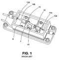
- Fig. 1 is a diagram of an optical package that is the result of years of development in an attempt to automate the assembly process and to lessen manufacturing costs while providing a relatively small, thermally stable optically packaged component. The goal was to provide a packaged component wherein performance would not significantly degrade over the expected lifetime of the device. Problems related to cost, and reliability have resulted in the abandonment of this solution.
- a non-linear frequency doubling crystal 10 performs filtering of an input signal and outputs a frequency doubled optical signal.
- optical fibers 12a and 12b held in sleeves must be precisely aligned so that light launched from the input fiber 12a to its output and through the frequency doubling crystal 10 must couple without undue loss into the output receiving optical fiber 12b and provide optimum filtering through the crystal 10.
- a frequency doubling optical component having an input optical fiber 12a held in an optical sleeve or ferrule 14a, optically coupled to a frequency doubling crystal 10, and optically coupled to an output optical fiber 12b.
- the optical sleeve 14a is held down in a fixed position by clamp 16 which is laser welded to a base member beneath.
- the optical crystal is secured to a holder 18 which is clamped to the base by a clamp 7.
- Bolts 9 secure sub-base members to the package. It is evident that the numerous interfaces between elements within the package increase the likelihood of misalignment of components. Furthermore, having this many elements and fasteners within this package lessens available space for other components.
- the package shown in Fig. 1 is conveniently shown before the top is positioned and hermetically seals the package.
- an optical fiber is housed within a sleeve and the sleeve is bonded to a base member, there is a possibility that there will be relative movement of the optical fiber and the sleeve. Furthermore, there is the possibility that there will be relative movement between the optical sleeve and the base member.
- the optical fiber is directly bonded to the base member, there is only the possibility of relative movement between the optical fiber and the base member. In this regard, it is preferable lessen the number of interfaces.
- a sealed container comprising;
- a method of manufacturing a sealed container comprising:
- Fig. 1 is a view illustrating a conventional packaged component having a plurality of interfaces.
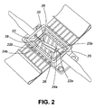
- Fig. 2 is a view of a packaged component in accordance with an embodiment of this invention wherein fewer parts and interfaces are required and wherein a filter is soldered to the package base.
- Fig. 3 is a schematic side view of a base member having an input lensed optical fiber optically aligned with an output optical lensed fiber having a PPLN (poled lithium niobate) crystal there between wherein the optical fibers and the crystal are soldered to their supporting members.
- PPLN poled lithium niobate
- Fig. 4 is a top view of the components shown in Fig. 3 .
- Fig. 2 a photograph of a non-sealed container in accordance with the invention is shown, prior to placing and hermetically sealing a lid in place over the device.
- the device of Fig. 2 provides the same functionality as the device of Fig. 1 .
- the device of Fig. 1 requires the thermal electric cooler to be outside of the package due to the limited space.
- an input optical fiber 22a is shown soldered in place on a base 21 precisely aligned with the non-linear frequency doubling crystal 20 and with the output optical fiber 22b.
- the solder ball made of AuSn (gold tin) 24a is shown resting upon a low pedestal 23a is preferably a Zr02 ceramic such as ytterbium stabilized zirconium, which is also soldered to the base 21 of the container. Only solder is present between the optical fiber 22a and an upper end of the pedestal 23a, and only solder is present between the lower end of the pedestal 23a and the base 21 of the container.
- the frequency doubling crystal 20 is also directly soldered to the base 21 upon which it rests, so that the planar lower surface of the crystal 20 securely mates with the container having only solder there between. This solder is applied by using a reflow technique.
- a similar arrangement is shown at the output end wherein optical fiber 22b is directly soldered to its respective pedestal 23b, which is directly soldered to the base 21 of the package. No ferrules are required to house and hold the optical fibers 22a and 22b, lessening the possibility of misalignment.
- a thermal electric cooler (TEC) 25 is disposed beneath the base 21 and within the package, so that efficient cooling and a more rapid cooling response time can be obtained. Electrodes 29 are provided to power the TEC 25. This particular device requires the temperature to be maintained at a predetermined temperature that is within +/-.01 C.
- a thermistor 26 is also disposed within the package on the base 21 for temperature monitoring.
- CTE coefficient of thermal expansion
- Figs. 3 and 4 illustrate the optical input and output optical fibers 32a, 32b, the pedestals or optical fiber mounts 33a and 33b, and the periodically poled lithium niobate frequency doubling crystal 30 in more detail.
- the optical fiber 32a has an output end adjacent to the crystal 30 shown to have a pointed or chiseled lens tip to focus and couple light from the fiber 32a to a region near the surface of the crystal 30. Furthermore, optical fiber 32a is securely mounted to the pedestal 33a via a single solder ball 34a, made of a solder with a relatively high melting temperature T h 295 C.
- the fiber mount 33a is secured to the base member 31 by way of having a very thin layer of solder between the mount 33a and the base member 31.
- a solder reflow technique is used to fixedly attach the base member 31 with the fiber mount 33a.
- the frequency doubling crystal 30 is also soldered to the base member 31; however, with a lower melting temperature solder, e.g.
- BiSn solder having a melting temperature of approximately 160C well below Th.
- the crystal 30 can be relatively moved and aligned during manufacture without the risk of moving the fiber mounts 32a and 32b, which are first secured to the base 31 with high melting temperature solder of about 295C, e.g. AuSn solder.
- the base member 31 which preferably consists of stainless steel, has a coefficient of thermal expansion (CTE) that is substantially matched to the CTE of the crystal 30 to less than 5 ppm/K.
- CTE coefficient of thermal expansion
- PPLN periodically poled lithium niobate
- SST403 is smaller than 2ppm/k. If the CTE of the crystal 30 was not suitably matched to the CTE of the base member, the crystal 20 would be adversely stressed upon cooling down from the 160 °C soldering temperature.
- this device can be manufactured using various alignment techniques, such as moving one optical fiber, e.g. 32a, while keeping the other optical fiber, e.g. 32b, and the crystal 30 fixed by first securing them with solder to the base 31. Preferably this is done while applying a signal to the device via one of the optical fibers and monitoring power at the output end. Once an optimum alignment is achieved the output fiber capturing the test light can be soldered in place.
- this invention provides a method and device wherein two optical fibers are aligned with an optical element where all three are fixed to a common base using solder.
Landscapes
- Physics & Mathematics (AREA)
- General Physics & Mathematics (AREA)
- Optics & Photonics (AREA)
- Optical Couplings Of Light Guides (AREA)
Abstract
A substantially thermally stable small optical package is disclosed which houses optically aligned elements forming an optical component. All of the elements are all directly soldered to a base member or directly soldered to a supporting member soldered to a common base member. The sealed container has a supporting base member made of stainless steel and a first optical fiber mount is directly soldered to the supporting base. A first optical fiber is directly soldered to the upper end of the first optical fiber mount. A similar arrangement is provided wherein a second optical fiber mount is directly soldered to the base and a second optical fiber is directly soldered to the upper end of the second optical fiber mount. A thin frequency doubling crystal is directly soldered to the stainless steel base member after being aligned with the two optical fibers. This design is extremely cost effective to manufacture and provides a component that is very thermally stable.
Description
- This application claims priority of
U.S. Provisional Patent Application No. 60/869,972 filed December 14, 2006 - This invention relates to a substantially thermally stable small optical package that houses a plurality of optically aligned elements forming an optical component, wherein the elements are all directly soldered to a base member or directly soldered to a supporting member soldered to a common base member.
- Optical devices and components operational within optical systems are typically subjected to various thermal and mechanical loads and or stresses during their lifetime. An example of such optical devices is an optical filter assembly. An assembly of this type comprises two optical glass fibers inserted into capillary ferrules to produce fiber-ferrule sub-assemblies aligned with an optical filter assembly. The optical components of the filter assembly generally have graded-index (GRIN) lenses embedded into an insulating glass tube, which in turn are mechanically protected by a metal housing. These filter assemblies often exhibit insertion losses higher than desired, resulting in degraded overall performance of the communications system or module. The problem is particularly acute during exposure to ambient operating conditions where temperature is variable.
- Input glass ferrules generally employ one of two designs. A single capillary suitable for containing multiple glass fibers or separate circular capillaries for each fiber have been used, each with relatively short fiber-receiving conical lead-in ends. With such input ferrules, the optical fiber is subjected to an unwanted S-bending over the short conical end. This excessive micro bending increases the insertion losses. Fiber-ferrule subassemblies employing such ferrules are manufactured by inserting the optical fibers stripped of their polymer coating into the respective ferrule capillaries; epoxy bonding the fibers into the ferrule capillaries, including the conical end portions; grinding and polishing an angled facet on the fiber-ferrule; and depositing on the polished surface an anti-reflection (AR) coating. Once finished, the fiber-ferrule is aligned and assembled with the collimating GRIN lens and then embedded into the insulating glass tube, which, in turn, is protected by a metal housing.
- In many instances adhesives are used to secure fiber-ferrules to a base or support member within their package. In some instances these fiber-ferrules are laser welded to a support member.
- A precise alignment achieved during initial assembly of a filter prior to final packaging can be easily decreased due to the adhesive curing process and the high temperature thermal cycles associated with laser welding during the final packaging of the components. Such manufacturing processes and resulting components have several problems resulting from stresses on the optical components due to the thermal contraction as a result of a thermal mismatch between the glass and metal materials, polymerization shrinkage in adhesive bonds, and structural constraints induced by bonding during encapsulation. These stresses lead to displacements of optical components during bonding, resulting in 0.3 to 1 dB or greater increases in the insertion loss.
- In an attempt to provide a packaged component that is thermally stable and that will perform to required specifications over the lifetime of the device, adhesives such as epoxies, or bonding by laser welding was not considered practicable. Each of these has their associated drawbacks. Although Laser welding requires little set-up time and setting time, post weld shift, a known problem, can cause fibers housed in sleeves welded to support members to shift.
-
Fig. 1 is a diagram of an optical package that is the result of years of development in an attempt to automate the assembly process and to lessen manufacturing costs while providing a relatively small, thermally stable optically packaged component. The goal was to provide a packaged component wherein performance would not significantly degrade over the expected lifetime of the device. Problems related to cost, and reliability have resulted in the abandonment of this solution. - In
Fig. 1 a non-linearfrequency doubling crystal 10 performs filtering of an input signal and outputs a frequency doubled optical signal. In the manufacture of the component,optical fibers input fiber 12a to its output and through thefrequency doubling crystal 10 must couple without undue loss into the output receivingoptical fiber 12b and provide optimum filtering through thecrystal 10. - In
Fig. 1 a frequency doubling optical component is shown, having an inputoptical fiber 12a held in an optical sleeve orferrule 14a, optically coupled to afrequency doubling crystal 10, and optically coupled to an outputoptical fiber 12b. Theoptical sleeve 14a is held down in a fixed position byclamp 16 which is laser welded to a base member beneath. The optical crystal is secured to aholder 18 which is clamped to the base by aclamp 7.Bolts 9 secure sub-base members to the package. It is evident that the numerous interfaces between elements within the package increase the likelihood of misalignment of components. Furthermore, having this many elements and fasteners within this package lessens available space for other components. The package shown inFig. 1 is conveniently shown before the top is positioned and hermetically seals the package. - It is apparent from looking at the device in
Fig. 1 , that there are numerous interfaces wherein components are fixedly coupled to other components, and wherein these other components must be relatively aligned and secured to a common base member. Furthermore, the use of adhesives, laser welding, soldering, and clamping were all required in the assembly of this device. - Understandably, the more components that hold other components within an optical package, the greater the probability for misalignment during the lifetime of the device.
- A simple scenario follows:
- If an optical fiber is housed within a sleeve and the sleeve is bonded to a base member, there is a possibility that there will be relative movement of the optical fiber and the sleeve. Furthermore, there is the possibility that there will be relative movement between the optical sleeve and the base member.
- However if the optical fiber is directly bonded to the base member, there is only the possibility of relative movement between the optical fiber and the base member. In this regard, it is preferable lessen the number of interfaces.
- When optical components made of crystalline material are to be fixedly secured to a base, secure bonding is essential, especially if a crystalline slab is to be optically aligned with an input and an output optical waveguide or optical fiber to maximize output power and to achieve a desired filtering such as frequency doubling. Furthermore, since this crystalline material is birefringent, it is important that the material does not undergo a change in stress as a result of temperature variation due to a thermal mismatch between the base and the crystalline material.
- Therefore, it is an object of this invention, to provide a package housing components wherein the components are optically aligned within certain tolerances, and wherein the components remain optically aligned within those tolerances.
- It is also an object of the invention to provide a package with fewer interfaces than in the prior art device shown in
Fig. 1 , and to provide a package which due to having fewer elements and interfaces, provides space to place a cooler/heater within the package to maintain the temperature of the components within predetermined tolerances. - This result of this improvement over the prior art, is a package which has a better cooling response time, and which is relatively inexpensive to manufacture while providing accurate alignment throughout the working life of the device.
- In accordance with an embodiment of the invention, there is provided, a sealed container, comprising;
- a) a supporting base member consisting of a first material;
- b) a first optical fiber mount having a height h1, wherein the first optical fiber mount has a lower end and an upper end;
- c) a first optical fiber directly soldered to the upper end of the first optical fiber mount;
- d) a second optical fiber mount having a lower end and an upper end and having a height h2;
- e) a second optical fiber directly soldered to the upper end of the second optical fiber mount; and,
- f) a thin optical element for modifying light passing therethrough mounted in the container, wherein the thin optical element has a planar bottom surface, and wherein the planar bottom surface is directly soldered to the base member, wherein only solder is present between the planar bottom surface and the base member, and, wherein the first and second optical fibers are aligned with the thin wafer so that light launched into one of the first and second optical fibers from an end extending from the sealed container passes through the thin optical element and exits the other of the first and second optical fibers extending out of the sealed container.
- In accordance with another aspect of the invention, there is provided, a method of manufacturing a sealed container, comprising:
- a) providing a supporting base member made of a first material;
- b) providing a first optical fiber mount having a height h1, wherein the first optical fiber mount has a lower end and an upper end;
- c) providing a first optical fiber;
- d) directly soldering the first optical fiber to the upper end of the first optical fiber mount;
- e) providing a second optical fiber mount having a lower end and an upper end and having a height h2;
- f) providing a second optical fiber;
- g) directly soldering the second optical fiber to the upper end of the second optical fiber mount; and,
- h) providing a thin optical element having a planar bottom surface, for modifying light passing therethrough; and,
- i) mounting the thin optical element in the container by directly soldering the planar bottom surface and the base member together, wherein the first and second optical fibers are aligned with the thin wafer so that light launched into one of the first and second optical fibers from an end extending from the sealed container passes through the thin optical element and exits the other of the first and second optical fibers extending out of the sealed container.
- Exemplary embodiments of the invention will now be described in conjunction with the drawings in which:
-
Fig. 1 is a view illustrating a conventional packaged component having a plurality of interfaces. -
Fig. 2 is a view of a packaged component in accordance with an embodiment of this invention wherein fewer parts and interfaces are required and wherein a filter is soldered to the package base. -
Fig. 3 is a schematic side view of a base member having an input lensed optical fiber optically aligned with an output optical lensed fiber having a PPLN (poled lithium niobate) crystal there between wherein the optical fibers and the crystal are soldered to their supporting members. -
Fig. 4 is a top view of the components shown inFig. 3 . - Turning now to
Fig. 2 a photograph of a non-sealed container in accordance with the invention is shown, prior to placing and hermetically sealing a lid in place over the device. The device ofFig. 2 provides the same functionality as the device ofFig. 1 . However the device ofFig. 1 requires the thermal electric cooler to be outside of the package due to the limited space. InFig. 2 an inputoptical fiber 22a is shown soldered in place on a base 21 precisely aligned with the non-linearfrequency doubling crystal 20 and with the outputoptical fiber 22b. The solder ball made of AuSn (gold tin) 24a is shown resting upon alow pedestal 23a is preferably a Zr02 ceramic such as ytterbium stabilized zirconium, which is also soldered to the base 21 of the container. Only solder is present between theoptical fiber 22a and an upper end of thepedestal 23a, and only solder is present between the lower end of thepedestal 23a and the base 21 of the container. Thefrequency doubling crystal 20 is also directly soldered to the base 21 upon which it rests, so that the planar lower surface of thecrystal 20 securely mates with the container having only solder there between. This solder is applied by using a reflow technique. A similar arrangement is shown at the output end whereinoptical fiber 22b is directly soldered to its respective pedestal 23b, which is directly soldered to the base 21 of the package. No ferrules are required to house and hold theoptical fibers Electrodes 29 are provided to power theTEC 25. This particular device requires the temperature to be maintained at a predetermined temperature that is within +/-.01 C. - Providing lenses on the end of the
optical fibers thermistor 26 is also disposed within the package on the base 21 for temperature monitoring. - The base member 21, preferably including or consisting of stainless steel, preferably KT- stainless steel SST 403, has a coefficient of thermal expansion (CTE) that is substantially matched to the CTE of the
crystal 20 to less than 5 ppm/K. If the CTE of thecrystal 20 was not suitably matched to the CTE of the base member, thecrystal 20 would be adversely stressed upon cooling down from the 160 °C soldering temperature. BiSn solder was used in securing thecrystal 20 to the base. -
Figs. 3 and 4 illustrate the optical input and outputoptical fibers 32a, 32b, the pedestals or optical fiber mounts 33a and 33b, and the periodically poled lithium niobatefrequency doubling crystal 30 in more detail. - In
Fig. 3 the optical fiber 32a has an output end adjacent to thecrystal 30 shown to have a pointed or chiseled lens tip to focus and couple light from the fiber 32a to a region near the surface of thecrystal 30. Furthermore, optical fiber 32a is securely mounted to thepedestal 33a via asingle solder ball 34a, made of a solder with a relatively high melting temperature Th 295 C. Thefiber mount 33a is secured to thebase member 31 by way of having a very thin layer of solder between themount 33a and thebase member 31. A solder reflow technique is used to fixedly attach thebase member 31 with thefiber mount 33a. Thefrequency doubling crystal 30 is also soldered to thebase member 31; however, with a lower melting temperature solder, e.g. BiSn solder, having a melting temperature of approximately 160C well below Th. Thus, thecrystal 30 can be relatively moved and aligned during manufacture without the risk of moving the fiber mounts 32a and 32b, which are first secured to the base 31 with high melting temperature solder of about 295C, e.g. AuSn solder. - This much more simple and elegant design having only solder joints to secure elements directly, without the use of tubes, sleeves, holders or clamps, provides a more robust device which is easier and less costly to manufacture.
- The
base member 31, which preferably consists of stainless steel, has a coefficient of thermal expansion (CTE) that is substantially matched to the CTE of thecrystal 30 to less than 5 ppm/K. The CTE difference between periodically poled lithium niobate (PPLN) and SST403 is smaller than 2ppm/k. If the CTE of thecrystal 30 was not suitably matched to the CTE of the base member, thecrystal 20 would be adversely stressed upon cooling down from the 160 °C soldering temperature. - Various alignment techniques can be used to manufacture this device, such as moving one optical fiber, e.g. 32a, while keeping the other optical fiber, e.g. 32b, and the
crystal 30 fixed by first securing them with solder to thebase 31. Preferably this is done while applying a signal to the device via one of the optical fibers and monitoring power at the output end. Once an optimum alignment is achieved the output fiber capturing the test light can be soldered in place. - The process for aligning the device in
Figs 2 and3 is performed by the following steps: - 1. Attaching the two fiber mounts (23a and 23b) and
thermistor 26 to the base element 21 using AuSn solder having a melting temperature of 295C using a hot plate. - 2. Attaching the base element (after step 1) to the top plate of TEC (25) and attaching the bottom plate of TEC to the bottom surface of the package using indium (160C) in a reflow oven; these two attachments are done in one step.
- 3. Attaching PPLN crystal waveguide sliver (20) to the top surface of the base element using BiSn (160C) on hot plate.
- 4. Wire bonding the TEC and thermistor to the package
- 5. Aligning the input fiber (22a) and soldering it on the fiber mount (23a) with AuSn (24a).
- 6. Aligning the output fiber (22b) and soldering it on the fiber mount (23b) with AuSn (24b).
- Advantageously, this invention provides a method and device wherein two optical fibers are aligned with an optical element where all three are fixed to a common base using solder. The numerous advantages of are described heretofore.
- Of course other embodiments can be envisaged without departing from the sprit and scope of this invention.
Claims (14)
- A sealed container, comprising:a) a supporting base member made of a first material;b) a first optical fiber mount having a height h1, wherein the first optical fiber mount has a lower end and an upper end;c) a first optical fiber directly soldered to the upper end of the first optical fiber mount;d) a second optical fiber mount having a lower end and an upper end and having a height h2;e) a second optical fiber directly soldered to the upper end of the second optical fiber mount; and,f) a thin optical element for modifying light passing therethrough mounted in the container, wherein the thin optical element has a planar bottom surface, and wherein the planar bottom surface is directly soldered to the base member, wherein only solder is present between the planar bottom surface and the base member, and, wherein the first and second optical fibers are aligned with the thin wafer so that light launched into one of the first and second optical fibers from an end extending from the sealed container passes through the thin optical element and exits the other of the first and second optical fibers extending out of the sealed container.
- A sealed container as defined in claim 1, wherein
the lower end of the first optical fiber mount is directly soldered to the base member so that only solder is present between the lower end of the first fiber mount and the base member; and,
wherein the lower end of the second optical fiber mount is directly soldered to the base member so that only solder is present between the lower end of the second fiber mount and the base member. - A sealed container as defined in claim 2, wherein h1, is approximately equal to h2.
- A sealed container as defined in claim 2, wherein the base support member is fixedly coupled to the bottom of the sealed container, and wherein the sealed container is hermetically sealed.
- A sealed container as defined in claim 2 wherein the CTE of the first material is matched to the CTE of the thin optical element to within 3-5 ppm/K.
- A sealed container as defined in claim 5 wherein the thin optical element comprises a crystalline material.
- A sealed container as defined in claim 5 wherein the thin optical element comprises a birefringent material.
- A sealed container as defined in claim 2 wherein the first and second fiber mounts are soldered to the base member with a first solder; and the thin wafer is soldered to the base member with a second solder, different from the first solder.
- A sealed container as defined in claim 8 wherein second solder has a lower melting point than the first solder to enable the first and second fiber mounts to be adjusted during assembly, while keeping the thin wafer fixed to the base
- A sealed container as defined in claim 9, wherein the second solder comprises BiSn solder; and wherein the first solder comprises AuSn solder.
- A sealed container as defined in claim 2 further comprising a thermal electric cooler disposed within the sealed container for cooling and maintaining the temperature within the sealed container to within predetermined limits.
- A sealed container as defined in claim 2 wherein the first material comprises stainless steel.
- A method of manufacturing a sealed container, comprising:a) providing a supporting base member made of a first material;b) providing a first optical fiber mount having a height h1, wherein the first optical fiber mount has a lower end and an upper end;c) providing a first optical fiber;d) directly soldering the first optical fiber to the upper end of the first optical fiber mount;d) providing a second optical fiber mount having a lower end and an upper end and having a height h2;e) providing a second optical fiber;f) directly soldering the second optical fiber to the upper end of the second optical fiber mount; and,g) providing a thin optical element having a planar bottom surface, for modifying light passing therethrough; and,h) mounting the thin optical element in the container by directly soldering the planar bottom surface and the base member together, wherein the first and second optical fibers are aligned with the thin wafer so that light launched into one of the first and second optical fibers from an end extending from the sealed container passes through the thin optical element and exits the other of the first and second optical fibers extending out of the sealed container.
- A method as defined in claim 13, wherein the solder used for soldering the thin optical element with the base member, has a lower melting temperature than the solder used to solder the first optical fiber with the first optical fiber mount.
Applications Claiming Priority (1)
| Application Number | Priority Date | Filing Date | Title |
|---|---|---|---|
| US86997206P | 2006-12-14 | 2006-12-14 |
Publications (1)
| Publication Number | Publication Date |
|---|---|
| EP1936414A2 true EP1936414A2 (en) | 2008-06-25 |
Family
ID=39269298
Family Applications (1)
| Application Number | Title | Priority Date | Filing Date |
|---|---|---|---|
| EP07254671A Withdrawn EP1936414A2 (en) | 2006-12-14 | 2007-12-01 | Small optical package having multiple optically aligned soldered elements therein |
Country Status (3)
| Country | Link |
|---|---|
| US (1) | US20080144997A1 (en) |
| EP (1) | EP1936414A2 (en) |
| CN (1) | CN101226317A (en) |
Families Citing this family (6)
| Publication number | Priority date | Publication date | Assignee | Title |
|---|---|---|---|---|
| CN104009378B (en) * | 2014-05-15 | 2017-03-29 | 深圳大学 | A kind of visible ray super continuum source based on green-light fiber laser pumping |
| JP2016161654A (en) * | 2015-02-27 | 2016-09-05 | 住友大阪セメント株式会社 | Substrate processing method using reinforcement member, and function element formed of substrate reinforced by reinforcement member |
| CN109164606A (en) * | 2018-09-19 | 2019-01-08 | 中国电子科技集团公司第二十六研究所 | A kind of fiber acouso optic device with high-performance stability |
| JP2019117397A (en) * | 2019-03-08 | 2019-07-18 | 住友大阪セメント株式会社 | Substrate processing method |
| US11768341B2 (en) * | 2019-09-18 | 2023-09-26 | Nippon Telegraph And Telephone Corporation | Package for optical module |
| CN115629443A (en) * | 2022-12-07 | 2023-01-20 | 武汉光谷航天三江激光产业技术研究院有限公司 | Packaging structure and packaging method of large-core-diameter high-power fiber grating |
Family Cites Families (7)
| Publication number | Priority date | Publication date | Assignee | Title |
|---|---|---|---|---|
| US5026138A (en) * | 1989-08-29 | 1991-06-25 | Gte Laboratories Incorporated | Multi-fiber alignment package for tilted facet optoelectronic components |
| FR2655161B1 (en) * | 1989-11-30 | 1992-12-24 | Cit Alcatel | DUAL OPTICAL COUPLING DEVICE, PARTICULARLY FOR FIBER OPTIC TRANSMISSION SYSTEM. |
| JP3409781B2 (en) * | 2000-09-05 | 2003-05-26 | 住友電気工業株式会社 | Method for manufacturing optical semiconductor module |
| US20020151113A1 (en) * | 2001-04-13 | 2002-10-17 | Hung Henry H. | Apparatus and method for suppressing false resonances in fiber optic modulators |
| US6773171B2 (en) * | 2003-01-14 | 2004-08-10 | Intel Corporation | Optoelectronic housings and methods of assembling optoelectronic packages |
| TWI278075B (en) * | 2004-08-17 | 2007-04-01 | Toshiba Corp | LSI package with interface module, transmission line package, and ribbon optical transmission line |
| JP4197668B2 (en) * | 2004-08-17 | 2008-12-17 | 株式会社東芝 | LSI package with interface module, interface module and connection holding mechanism |
-
2007
- 2007-12-01 EP EP07254671A patent/EP1936414A2/en not_active Withdrawn
- 2007-12-10 US US11/953,448 patent/US20080144997A1/en not_active Abandoned
- 2007-12-14 CN CNA2007103012053A patent/CN101226317A/en active Pending
Also Published As
| Publication number | Publication date |
|---|---|
| CN101226317A (en) | 2008-07-23 |
| US20080144997A1 (en) | 2008-06-19 |
Similar Documents
| Publication | Publication Date | Title |
|---|---|---|
| KR920010947B1 (en) | Optical coupling device and manufacturing method thereof, light emitting device and assembly method thereof, and lens holder | |
| US5627931A (en) | Optoelectronic transducer | |
| US4948219A (en) | Method of connecting optical fibers and connection aids and fiber holders employed therewith, and optical waveguide modules employing same | |
| US5661835A (en) | Optical composite module and method of assembling the same | |
| CN1275062C (en) | Fixture of optical element in photoelectric package | |
| EP1936414A2 (en) | Small optical package having multiple optically aligned soldered elements therein | |
| US6019522A (en) | Optical part packaging method and collimator assembly method | |
| CN101216575B (en) | Polarization maintaining fiber pigtail assembly | |
| US6603906B2 (en) | Multi-port optical power monitoring package and method of manufacturing | |
| JP3518491B2 (en) | Optical coupling device | |
| US6513992B2 (en) | Planar fiber optical housing | |
| JPS60136387A (en) | Optical element module | |
| US6550984B2 (en) | Integrated optical component with photodetector for automated manufacturing platform | |
| JP5324371B2 (en) | Optical connection component and optical connection method | |
| JP2013231895A (en) | Optical module | |
| JP5291033B2 (en) | Optical parts | |
| JP3301197B2 (en) | Parallel transmission module and manufacturing method thereof | |
| Becker et al. | Rugged, low-cost pigtailing approach for LiNbO/sub 3/integrated optic devices | |
| JP4364016B2 (en) | Array type photo detector | |
| CN117250696A (en) | High-speed Fabry-Perot tunable filter based on the inverse piezoelectric effect of piezoelectric single crystal | |
| JP2003215514A (en) | Variable optical attenuator, method of manufacturing the same, and optical module | |
| JPH07120639A (en) | Method of manufacturing waveguide module and optical waveguide module | |
| KR100470912B1 (en) | Method for manufacturing packaging in micro optics optical filter | |
| KR100319911B1 (en) | Optical package and its fixing method | |
| JPS6059309A (en) | Optical element coupling module |
Legal Events
| Date | Code | Title | Description |
|---|---|---|---|
| PUAI | Public reference made under article 153(3) epc to a published international application that has entered the european phase |
Free format text: ORIGINAL CODE: 0009012 |
|
| AK | Designated contracting states |
Kind code of ref document: A2 Designated state(s): AT BE BG CH CY CZ DE DK EE ES FI FR GB GR HU IE IS IT LI LT LU LV MC MT NL PL PT RO SE SI SK TR |
|
| AX | Request for extension of the european patent |
Extension state: AL BA HR MK RS |
|
| STAA | Information on the status of an ep patent application or granted ep patent |
Free format text: STATUS: THE APPLICATION IS DEEMED TO BE WITHDRAWN |
|
| 18D | Application deemed to be withdrawn |
Effective date: 20100701 |