EP1933933B1 - Mri-safe high impedance lead systems - Google Patents
Mri-safe high impedance lead systems Download PDFInfo
- Publication number
- EP1933933B1 EP1933933B1 EP06817232.9A EP06817232A EP1933933B1 EP 1933933 B1 EP1933933 B1 EP 1933933B1 EP 06817232 A EP06817232 A EP 06817232A EP 1933933 B1 EP1933933 B1 EP 1933933B1
- Authority
- EP
- European Patent Office
- Prior art keywords
- conductors
- high impedance
- lead
- lead system
- conductor
- Prior art date
- Legal status (The legal status is an assumption and is not a legal conclusion. Google has not performed a legal analysis and makes no representation as to the accuracy of the status listed.)
- Active
Links
Images











Classifications
-
- A—HUMAN NECESSITIES
- A61—MEDICAL OR VETERINARY SCIENCE; HYGIENE
- A61N—ELECTROTHERAPY; MAGNETOTHERAPY; RADIATION THERAPY; ULTRASOUND THERAPY
- A61N1/00—Electrotherapy; Circuits therefor
- A61N1/02—Details
- A61N1/04—Electrodes
- A61N1/06—Electrodes for high-frequency therapy
-
- A—HUMAN NECESSITIES
- A61—MEDICAL OR VETERINARY SCIENCE; HYGIENE
- A61N—ELECTROTHERAPY; MAGNETOTHERAPY; RADIATION THERAPY; ULTRASOUND THERAPY
- A61N1/00—Electrotherapy; Circuits therefor
- A61N1/02—Details
- A61N1/04—Electrodes
- A61N1/05—Electrodes for implantation or insertion into the body, e.g. heart electrode
- A61N1/056—Transvascular endocardial electrode systems
-
- A—HUMAN NECESSITIES
- A61—MEDICAL OR VETERINARY SCIENCE; HYGIENE
- A61N—ELECTROTHERAPY; MAGNETOTHERAPY; RADIATION THERAPY; ULTRASOUND THERAPY
- A61N1/00—Electrotherapy; Circuits therefor
- A61N1/02—Details
- A61N1/08—Arrangements or circuits for monitoring, protecting, controlling or indicating
- A61N1/086—Magnetic resonance imaging [MRI] compatible leads
Definitions
- the present invention relates to interventional medical leads and may be particularly suitable for MRI compatible implantable devices such as cardiac pacing devices and Deep Brain Stimulation ("DBS”) and/or sympathetic nerve chain stimulation leads.
- DBS Deep Brain Stimulation
- DBS deep brain stimulation
- CP cardiac pacing
- RF Radio Frequency
- RF/microwave diathermy treatments can use leads that employ an alternating current to cauterize tissue.
- the diathermy alternating current delivered during the therapy can be in the range of between about 1KHz-350 MHz (believed to be typically at about 27.5 MHz).
- the lead system may undesirably act as an antenna, receiving and depositing current in localized tissue where the leads are exposed, thereby potentially increasing the specific absorption rate (SAR) (a way of measuring the quantity of radiofrequency (RF) energy that is absorbed by the body).
- SAR specific absorption rate
- RF heating of tissue in close proximity to long conductors (such as metallic wires) in an MRI environment has also been reported in literature. Local tissue damage can be caused by RF deposition in the tissue that is in close proximity to the linear conductors or electrodes of the lead system, when patients with implanted leads or interventional devices are placed in an external RF field.
- This RF heating mechanism may be explained as follows. During an MRI scan, the transmit RF field creates a voltage along the long linear conductors (individual or part of any interventional device) or the conductors/filers of the DBS and cardiac pacing lead systems. Currents are then created through the conductors and into the surrounding tissue. Where the current emerges from the distal tip of the device (or adjacent to the electrode in the case of an implantable lead), it can be concentrated and can cause heating and subsequent tissue damage.
- the present invention relates to MRI/RF compatible medical devices as defined in independent claim 1. Embodiments of the invention are recited in the dependent claims.
- Some embodiments of the present invention provide therapeutic lead systems that exhibit high impedance during exposure to RF (high frequencies).
- the lead systems can be used with interventional devices and may be acutely placed in vivo or chronically implantable and can include one or more stimulating, ablating and/or recording electrode.
- the lead systems may be particularly suitable for implantable lead systems for IPGs (implantable pulse generators), cardiac defibrillators, cardiac pacing (CP), neurostimulation (peripheral, deep brain, or spinal), EP catheters, guidewires, and the like, for leads used in heat-sensitive regions in the body.
- the lead systems may be implantable, MRI compatible multi-purpose lead systems with at least one stimulating/pacing electrode and may optionally be configured to provide an internal MRI receive antenna.
- the lead systems include a plurality of high impedance sections or segments spaced along the length of the lead.
- the high impedance sections are configured as RF traps that inhibit flow of induced RF current at the high impedance frequency/frequencies, whereby current is inhibited from heating tissue adjacent to one or more electrodes, thus reducing the likelihood of and/or preventing RF-current induced tissue damage.
- the RF traps can be configured to allow physiological and stimulation signals to pass through (typically in the kHz range). Thus, the RF trap traps only the high frequencies of interest to which the traps are tuned.
- Embodiments of the invention describe different methods of creating high impedance RF traps using the components of an implantable lead system or a medical device.
- the RF traps are incorporated in long metallic components to render them safe to use in an MRI environment.
- the lead systems may include supplemental high impedance circuits for the shield in combination with the high impedance configurations for conductors.
- Some embodiments are directed to interventional devices and/or implant devices comprising metal or metallic components.
- a lead can be a relatively long implantable lead having a length in the body of greater than 10 cm.
- the at least one electrode can be a plurality of electrodes with at least one being a recording and/or a recording and stimulating and/or ablating electrode.
- Some embodiments are directed to MRI/RF compatible medical interventional devices.
- the devices include an implantable elongate lead system having at least a first and a second electrode, each associated with a respective first and second axially extending conductor.
- a plurality of axially spaced apart capacitors are disposed between the first and second axially extending conductor along at least major portion of a length of the lead system to define a plurality of high impedance circuit segments whereby the lead system has a high impedance over a target range of (typically a high range) of radiofrequencies and a low impedance over another range of low electromagnetic frequencies (such as audio-frequencies or frequencies in the kHz or lower ranges, including DC at around 0 Hz).
- the high impedance circuit segments are configured to inhibit RF transmission along the lead system during exposure to RF associated with a high-field magnet MRI system.
- MRI compatible device/lead systems that include:
- the surface band gap structure may include a primary shield and secondary and tertiary segmented shields which are intermittently connected to the primary shield, whereby the high impedance surface reduces or blocks RF propagation.
- an MRI compatible device that includes: (a) an implantable lead system elongate lead having at least a first and a second electrode, each associated with a respective first and second axially extending conductor, wherein a plurality of spaced apart capacitors are disposed between the first and second axially extending conductors along at least major portion of a length of the lead system to define a plurality of high impedance circuit segments; and (b) a high impedance band gap surface formed along at least a major length of the lead system.
- the lead system has a high impedance at a high range of radiofrequencies and a low impedance at a low range of frequencies.
- IPG implantable pulse generators
- the controller is remotely controllable to activate the decoupling circuit to provide the high impedance.
- the high impedance circuits and/or circuit segments may comprise inductors.
- Inductors and capacitors can be formed from conducting leads and a dielectric substrate and can be configured to reduce, block or inhibit RF transmission along the lead system during exposure to RF associated with a high-field magnet MRI system, while permitting passage of low frequency physiologic signals, treatments and/or stimuli.
- the lead may be a flexible lead and the at least one electrode can be a plurality of spaced apart electrodes.
- the lead can include a plurality of conductors held in a core of the lead, a respective one for each electrode.
- Some examples which do not form part of the present invention, are directed to MRI-safe lead systems that include:
- Some examples which do not form part of the present invention, are directed to MRI-safe lead systems that include:
- Some examples which do not form part of the present invention, are directed to MRI-safe lead systems that include an elongate flexible body with a plurality of conductors and at least one high impedance segment with opposing proximal and distal portions.
- the at least one high impedance segment is configured so that at least one of the conductors has (a) a first individually coiled segment that is proximate to but axially apart from the coiled segments of different leads, and (b) a second coiled segment that is co-wound with at least one other conductor coiled segment.
- a conductive shield resides over the first lead first and second coiled segments and an insulating material resides between the shield and the first and second coiled segments.
- the at least one lead with the individual and co-wound coiled segments is in electrical communication with the shield at a proximal portion of the high impedance segment.
- high radiofrequency or “high RF” refers to RF frequencies that are at or above about 1 MHz, and includes radiofrequencies in the range of about 1MHz to about 256 MHz.
- Embodiments of the present invention configure devices so as to have high impedance circuit segments or a high impedance circuit at high RF and low impedance circuit segments or circuit at DC or low frequency (at a kHz or less frequency or frequency range), i.e., at frequencies used for treatment such as stimulation or ablation.
- the respective frequencies are 64 MHz, 128 MHz and 256 MHz.
- the frequencies of the different MRI systems are well known to those of skill in the art.
- the devices can be configured to have high impedance at several of the radiofrequencies associated with high-field magnet MRI systems, such as systems with magnets above about 1.0T, such as about 1.0T, 1.5T, 2.0T, 3.0T, 4.0T, 5.0T, 6.0T and 9.0T, typically between about 1T to 15T.
- high impedance means an impedance sufficiently high to inhibit, block or eliminate flow of RF-induced current at a target frequency range(s).
- the impedance has an associated resistance and reactance as is well known to those of skill in the art. Some embodiments provide an impedance of at least about 300 Ohms, typically between about 400 Ohms to about 600 Ohms, such as between about 450 Ohms to about 500 Ohms, while other embodiments provide an impedance of between about 500 Ohms to about 1000 Ohms.
- Embodiments of the invention configure lead systems that provide sufficiently high-impedance at frequencies associated with a plurality of different conventional and future magnetic field strengths of MRI systems, such as at least two of 1.5T, 2.0T, 2.5T, 3.0T, 9.0T, and the like, allow for safe use in those environments (future and reverse standard MRI system compatibility).
- tuned means that a parallel resonant circuit with inductive and capacitive characteristics defined by certain components and configurations has a high impedance at one or more target frequencies, typically including one or more MRI operating frequencies.
- coil segment refers to a conductive lead (trace, wire or filar) that has a coiled configuration.
- co-wound segments means that the affected leads, conductors, wires and/or filars can be substantially concentrically coiled at different radii, one above the other, or concentrically coiled closely spaced at substantially the same diameter.
- co-wound is used to describe structure and is not limiting to how the structure is formed (i.e., the coiled segments are not required to be wound concurrently or together, but may be so formed).
- conductive element refers to a conductive path that connects target components (such as, for example, a stimulation source and an electrode) and can include one or combinations of a metallic trace, a wire, a flex circuit, a filar(s), or other conductive configuration.
- the conductors or conductive elements include long linear and/or non-linear conductors that can be formed with one or more of discrete wires, flex circuits, filars (bi, quadra or other winding), or by plating, etching, deposition, or other fabrication methods for forming conductive electrical paths.
- Embodiments of the present invention can be configured for any desired internal region of the body or object.
- the object can be any object, and may be particularly suitable for animal and/or human subjects.
- Some embodiments can be sized and configured for brain stimulation, typically deep brain stimulation.
- Some embodiments can be configured to stimulate a desired region of the sympathetic nerve chain and/or the spinal cord.
- Some lead or implantable devices can be configured for cardiac intervention.
- Other embodiments may be directed to other anatomical structures, organs or features including deep tissue, lumens, and the like.
- the systems of the present invention may be configured for treatment of gastrointestinal, urinary, or other body regions.
- Some embodiments provide devices configured for intraluminal or intratissue penetration.
- Some embodiments provide devices for acute or chronic implantation.
- the extent to which the lead system or the long conductor couples with the external RF is a function of length of the lead system or the conductor, the insulation thickness over it and its arrangement in the RF field e.g. looping, etc.
- lengths shorter than quarter wavelength (at the applied RF frequency) do not couple with the external RF fields, displaying reduced RF deposition and lower local temperature rise in tissue adjacent to them.
- increasing the insulation thickness can reduce the coupling and RF deposition in the adjacent tissue.
- Linear conductors/wires act as linear antennas.
- Lead systems which have more than one long conductor act as linear antennas, where each individual conductor acts as an antenna and two or more conductors in combination with each other act as antennas too. This creates a RF coupling pattern having the lead system couple at multiple/different frequencies.
- DBS and cardiac pacing leads may comprise about 8 (and may include more or less) long conductors and electrodes. In particular embodiments, one, some or all of the conductors can act as antennas individually and in combination with each other.
- Internal and external imaging coils used in MRI can be decoupled during RF transmit by the scanner. This can inhibit local heat deposition in the tissue adjacent to the coils.
- the decoupling mechanism can create a high impedance circuit so that these coils do not couple with the transmitted RF, thus eliminating any tissue damage. See, Yoda K., Decoupling technique for transmit coils in NMR spectroscopy and imaging,. NMR Biomed 1990;3(1):27-30 ; and Buchli et al., Increased RF power absorption in MR imaging due to RF coupling between body coil and surface coil, Magn Reson Med 1989; 9(1):105-112 .
- standing wave formation on long coaxial cables may be attenuated by incorporating balun circuits or RF chokes at various locations on the shield of coaxial cables. See, Atalar et al., U.S. Patent No. 6,284,971 , entitled, Enhanced Safety Coaxial Cables.
- this application describes incorporating RF chokes on DBS and CP lead systems.
- Shielding linear conductors can inhibit RF deposition on them.
- This shielding can be continuous, discontinuous, or may be achieved by multiple methods, to list a few, e.g., insulating conductors with polymers filled with conducting metals doped for conductivity.
- a high impedance lead assembly 20 can employ at least one conductor 20c, shown as two conductors 1, 2 which may be coiled ( Figure 1B ) and/or reside parallel ( Figure 1A ) to each other, or be configured with combinations of both, and that are operational over a relatively wide range of frequencies.
- These long conductors 20c can have a metal core and are typically insulated from each other along their length and may be surrounded by a polymeric dielectric 20i. At intermediate locations, the two conductors 1, 2 are connected by capacitors 3.
- the combination of the length of the conductors 1 and 2 (which can also form inductors) and the capacitors 3 is configured to create a high impedance circuit(s).
- This circuit is configured so that it does not tune to a target range of RF frequencies, including for example, frequencies ranging from about 1 MHz to 250 MHz, creating high impedance circuit segments, thus reducing the extent of coupling in this frequency range.
- the circuit has high impedance to high RF, but has low resistance to DC, or low frequency RF (KHz), which is the stimulation frequency.
- KHz low frequency RF
- This principle may be applied to designing RF/MRI-safe devices and/or lead systems for CP leads, DBS leads, spinal cord stimulation leads, etc.
- the capacitors 3 can be regularly spaced or irregularly spaced.
- the capacitors 3 may have the same or different capacitance from each other.
- Lead systems 20 can comprise a plurality of electrodes and conductors, such as between about 2 to about 10 conductors, typically at least about 4. In some embodiments, the lead systems can include about 8 conductors.
- the conductor axial lengths can range from about 10 to 200 cm, with a thin insulator layer on the conductors and with a polymeric dielectric insulator layer over it.
- the conductors 20c can be connected to electrodes 100 1 , 100 2 , which, in position, can be in contact with target tissue.
- the conductors 20c run along the length of the lead system and are terminated by connecting to electrodes 100 1 and 100 2 at the distal end. At the proximal end these conductors are connected to the pulse generator (IPG).
- IPG pulse generator
- the conductors are typically made of stainless steel or other conducting non-ferromagnetic material.
- two (straight/linear) parallel conductors 8 and 9 are connected to each other at intermediate locations by capacitors 10 along the length of the lead system to form high impedance sections.
- the capacitors 10 can be semiconductor-based discrete products or can be otherwise provided, such as using coatings of metal oxides, e.g . tantalum oxide, and the like at discrete certain locations so as to connect the two conductors 8, 9 at desired locations.
- Figure 3C similar to Figure 3A , illustrates two parallel conductors but as wound conductors 1, 2 with spaced capacitors 3 in communication therewith and two respective electrodes 100 1 , 100 2 .
- more than one high impedance circuit can be formed with different conductor pairs.
- FIG 4 where there are three electrodes 100 1 , 100 2 , 100 3 and three conductors 20c, labeled as elements, 8, 9, and 12, respective capacitors 10 can be disposed between conductor pairs ( 8, 12 or 12, 9, as shown).
- one conductor 20c may be used in combination with two conductors to form two separate high impedance circuits.
- the lead systems 20 can conduct DC or a low frequency AC (KHz), typical of stimulation current.
- the conductors 20c may be made of any suitable (MRI compatible and/or non-ferromagnetic) conducting material and/or metal, e.g., Nitinol, Cobalt-Chromium alloy, MP35N alloy, gold, silver, platinum, platinum-iridium alloy, stainless steel, copper and other non-ferromagnetic materials, which will not cause a susceptibility artifact in MRI or magnetically react to the magnetic field in an MRI scanner environment.
- DC conductivity is a bulk phenomenon and RF conductivity is a skin depth phenomenon.
- the RF conductivity of the lead system may be reduced by using composite wire (a conductor or wire formed of a combination of different conductive materials) such as by using a resistive metal such as tungsten, MP35N or Nitinol wire on the outside and with a conductive core formed of gold, silver or copper or other metals.
- composite wire a conductor or wire formed of a combination of different conductive materials
- a resistive metal such as tungsten, MP35N or Nitinol wire
- a conductive core formed of gold, silver or copper or other metals.
- these leads made of composite wires can have an insulator coating on the outer surface and may be connected by capacitors to form high impedance RF circuits along the length of the lead system as described above with respect to Figures 1-4 .
- Figures 5A and 5B illustrate lead systems formed with high impedance segments of two or more insulated conductors 20c with any single conductor and/or a composite conductor structure having a polymeric layer 13 over them.
- the leads may be further shielded by a polymeric dielectric material with metal or conductive particulates 13c ( Figure 5A ) dispersed therein to shield/deflect external RF.
- the polymeric dielectric or insulation 13c over the conductors 20c may be filled/dispersed or mixed with another high dielectric constant material, e.g. , titanium dioxide, etc., to regulate the impedance between (two or more) conductors.
- conductive shielding 325 as a continuous or discontinuous conductor layer (braided, coated, etc) may be applied over the conductors 20c of the lead system as shown in Figure 5B .
- An insulating polymeric material 13 may reside between the conductors 20c 1 , 20c 2 and the shield 325.
- a polymer outer layer 21 may encase the lead system 20.
- RF chokes 64rf as described in WO 2006/031317 , filed August 9, 2005 , entitled, Implantable MRI Compatible Stimulation Leads and Antennas and Related Systems and Methods, may be incorporated over these high impedance segments or leads to further prevent formation of standing RF waves.
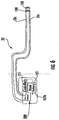
- an IPG 102 can have a lead system 20 with multiple conductors 20c that connect distal electrodes 100.
- the IPG may optionally include a decoupling circuit 200 which can be incorporated in an implanted housing of the IPG 102 and/or in a connector or portion of the IPG lead assembly (a connector or end portion of the lead assembly rather than the housing itself).
- the IPG 102 can include a power source 102b, such as a battery.
- the circuit 200 can be in communication with a digital controller 121 that can programmatically activate the circuit 200 (and/or deactivate the circuit 200 ).
- the lead system 20 may optionally be arranged as an antenna described earlier with two or more capacitor sets per antenna.
- Implantable IPGs can be used with other lead system configurations which do not form part of the present invention (see, e.g., Figures 15-22 ) .
- the lead system can be transformed to a high impedance lead (and/or antenna) by activating the decoupling circuit 200 to a short circuit, before an MRI scan or exposure to external RF.
- This activation can create a high impedance circuit with the capacitors and inductor assembly in the lead body making the lead electrically invisible to the external RF thus reducing coupling with the RF.
- the decoupling may comprise a single or multiple circuits tuned to different frequencies and can be programmed to be activated accordingly.
- the activation and/or adjustment to different RF frequency and/or deactivation can be carried out by a wireless command sent to the IPG.
- the activation may be carried out internally (automatically) in response to detection of an RF signal.
- Some lead systems 20 of the instant invention can be configured so that one or more conductors behave as inductors or comprise inductive components.
- the inductors can be provided by coiled conductor (wire) segments, flexible dielectric substrates, or other inductor configurations.
- capacitors can act as shorts and may not, by themselves, give sufficiently high impedance.
- the lead systems 20 can include inductors that cooperate with the capacitors.
- the leads or conductors of the systems can have high impedance at high frequency and low impedance at low frequency by configuring the conductors (wires/leads) to behave as inductors.
- At least one conductor 20c of the lead system 20 comprises a wound coil segment of the at least one conductor to define a coil inductor.
- the coil inductor may be wound to encase other another conductor(s) of the lead system.
- the coil inductor can be formed as substantially an entire length of a first conductor or as a smaller portion of the conductor.
- the capacitors can connect sections of the coil inductor and a second conductor.
- Figures 7 and 8 are graphs of data associated with a 12 cm long coiled inductor pair open at both ends when loaded in saline.
- the conductors are 32 AWG magnet wire closely wound on a 0.020 inch mandrel.
- the graph shows an X-axis frequency sweep from 1.0 to 150 MHz.
- the two-conductor assembly tunes at different frequencies to different extents as represented by the arrows in Figure 8 .
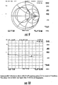
- Figures 9 and 10 illustrate the same parallel inductors as described above ( Figures 7 and 8 ) with 0.5 pF capacitors placed at about 2.5 cm apart at 5 locations.
- the return loss is flatter and higher than -8 db for all frequencies. It is contemplated that this loss can be further reduced (closer to zero) in an optimized design.
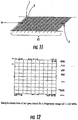
- Figure 11 is a schematic diagram of the parallel inductors with the inductor coil 1 being the wider outside strip and the inductor coil 2 being the inner strip (slightly thinner).
- the 0.5 pF inductors (3, 4) are shown positioned between the two inductors 1, 2 to create a high impedance system at the frequency range or ranges of interest.
- Figure 12 is a graph of a sample return loss of an open circuit for a frequency range of between about 1-150MHz.
- FIG. 13A illustrates an example of an MRI/RF safe lead system with an IPG connector 22 and IPG electrical connections 23, which system is not per se an embodiment of the present invention.
- the lead system 20 includes a plurality of electrodes 100, respective conductors/wires 20c, a primary shielding 33, a segmented secondary shielding 34, segments /inductors 35, and a segmented tertiary shield 36.
- the segments/inductors 5 connect the secondary 34 and tertiary shield 36 to the primary shield 33.
- the lead system 20 and/or the conductors 20c of the lead system are shielded by one or more layers of shield arrangements as shown in Figure 13A .
- This may be defined as a "3-D RF band gap structure" 39 which is an RF open circuit, while being a DC (and/or potentially a low frequency AC) short circuit.
- This structure can include a thin, typically two-dimensional, pattern of capacitive and inductive elements, which act as miniature parallel resonant circuits which block RF propagation.
- the conductors 20c can be coiled individually or co-wound, or combinations of each. At one end portion, typically a proximal end portion of the segment, the conductors 20c can be selectively connected to the high impedance shield directly or indirectly in a capacitor which act as an RF open and low frequency (DC) open circuit.
- DC RF open and low frequency
- Figure 13B illustrates a side view of the device shown in Figure 13A .
- Figure 13C is a cross-sectional view.
- a polymer dielectric insulating overcoating 21 can be applied to the lead system 20.
- dielectric/insulation layers 46, 48, 40 may be disposed intermediate the shielding layers 33 (primary shield), 34 (segmented secondary shield), and 36 (segmented tertiary shield).
- the conductors 20c extend to connector 22 and electrical connections 23 to the IPG or other stimulation, ablation or recording device.
- Capacitors 24 ( Figure 13A ) are not required according to some examples , as the segmented shielding configurations and inductor lead configuration may provide suitable impedance at high frequency. It is emphasised that such examples do not form part of the present invention.
- FIG 14 illustrates an electrode arrangement with RF chokes 64rf that can be used with high impedance circuits/segments and configurations described and/or shown herein.
- Each electrode 100 is typically in communication with at least one of the insulated conductors 20c.
- the conductors 20c are connected to a connector 22 with electrical connections 23 so as to be connected to the implantable signal generator 102 or to an external circuit, such as an interface circuit 40 during MRI guided lead/cable placement.
- the lead support body 20 need not be able to provide MRI signals ( i.e., it can optionally be configured with an MRI receive antenna).
- These insulated conductors 20c are typically covered with a polymeric insulator sleeve 61 and a conducting material is cylindrically layered to form the first shielding layer 62 over the insulator.
- This shielding 62 may be terminated proximal to the electrodes 100 and, in this embodiment, may not be in electrical contact with the conductors and/or the electrodes.
- a second insulator/polymeric/dielectric layer 63 further insulates this shielding 62 to form multi-core coaxial type cable system, with an impedance that is typically between about 10-100 ohms.
- the RF chokes 64rf can be integrated or built into the shielding 64 in the form of a second shielding, which is not continuous and has multiple sections each ⁇ /4 or less in length. As shown in Figure 14 , at the proximal end, each section or segment 64s is connected to the primary shielding 62, and the distal end may not be electrically connected to the primary shielding 62, or is connected with a capacitance 164 in between the primary and secondary shielding 62, 64, respectively.
- a top insulator/polymeric layer 65 can be used to insulate the body 20b, except for the electrodes 25.
- the MRI active portion of the antenna 35 may extend between a location where the primary shield 62 terminates and the first electrode 25 1 .
- the second shield layer 64 comprises a plurality of axially spaced apart RF chokes 64rf.
- the term "RF chokes" refers to a shielding layer configuration that provides an electrical length of less than or equal to ⁇ /4 (from the perspective of external electromagnetic waves) to inhibit the formation and/or propagation of RF induced current or standing waves in an AC (alternating current, e.g., diathermy applications) or RF exposure environment.
- the physical length that provides the electrical wavelength may vary depending on the materials used in fabricating the catheter or lead system support body (such as dielectric constant) and the magnetic field in which it is used.
- the lead system 20 has a physical length that is greater than 10 cm, typically between about 20 cm to about 150 cm.
- the implantable lead segment 50 can also include RF chokes 64rf formed along target regions or along substantially the entire implantable length.
- the RF chokes 64rf comprise a plurality of disconnects of the shield 64 and/or discrete electrically isolated second shield segments.
- the RF chokes 64rf can include a series of axially spaced apart Balun circuits or other suitable circuit configurations. See, e.g., U.S. Patent No. 6,284,971 for additional description of RF inhibiting coaxial cable that can inhibit RF induced current.
- the second shield layer 64 may be coupled to the first shielding layer 62 at opposing ends of the segments 64s. As shown, one end (typically the proximal end portion) of the disconnected segment 64s is directly coupled to the shielding layer 62 and the other end (typically the distal end portion) is capacitively coupled to the first shielding layer 62. Each segment 64s may be configured to engage the first shield layer 62 in the same manner or in an opposing different electrical manner (not shown).
- FIGS 15A-15B illustrate lead systems 20 with at least one high impedance segment 300 with associated axially spaced apart proximal and distal portions, 330p, 300d, respectively. These lead systems are not configured in accordance with the present invention.
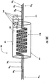
- the high impedance segment 300 can be described as an RF trap that includes a conductor 20c being coiled to define an inductor 310 within a conductive shield 325 and with an insulator/dielectric material 330 between the inductor 310 and shield 325.
- the conductor 20c can be in electrical communication with the conductive shield 325 at one end (shown in Figure 15A as the proximal end portion 300p ) of the high impedance segment 300.
- the implantable lead system can include multiple high impedance sections or segments 300 along the length of the lead.
- the high impedance sections or segments are created by arranging the components of the medical device, i.e., the conductor, etc. as an RF trap.
- These high impedance RF traps inhibit the flow of induced RF current (at the frequency to which the RF trap is tuned) and prevent it from heating tissue adjacent to the electrodes, thus minimizing or preventing RF induced tissue damage. Since the physiological and stimulation signals are at low frequencies (KHz range), the RF trap allows the lower frequency signal(s) to go through, trapping only the higher frequencies of interest to which the traps are tuned.
- the conductor 20c can be in electrical communication with the shield at the distal portion of the high impedance segment 300 via a tuning capacitor 340.
- the high impedance segment 300 e.g., RF trap
- the segment 300 can also be configured so that the conductor 20c at the proximal end portion of the segment 300p is connected to the shield 325 via a capacitor 360.
- Different high impedance segments 300 may be tuned to different MRI frequencies ( i.e., 64 MHz and 128 MHz or other standard operating frequencies of commercial MRI scanners).
- the impedance of the segment 300 can be at least 400 Ohms, typically greater than about 450 Ohms.
- the at least one high impedance segment 300 can be placed at between about 0.1-12 cm from the electrode(s) 100.
- the lead 20c can be configured with a straight segment 311 that merges into the coiled segment 310.
- the RF trap 300 with the shield 325, inductor 310 and tuning capacitor 340 form a high impedance parallel resonant circuit at the desired frequency to block RF currents along the conductor.
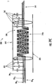
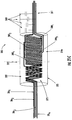
- the tuning capacitor can include one or more of a discrete capacitor 340 ( Figure 15A ) and/or stray capacitance 350 ( Figure 15B ) between the inductor 310 and the shield 325.
- Figure 15B illustrates that the high impedance segment 300 may include stray capacitance 350 that resides between the conductive shield 325 and the inductor 310 through the insulator/dielectric 330.
- the stray capacitance 350 and/or the discrete capacitor 340 can be used to tune the RF trap to a high-impedance at a desired frequency (range), typically between 1MHz to 250MHz.
- Another capacitor 360 may also be used at the opposing end of the segment 300 to form an RF short (not shown).
- the high impedance segment 300 can be tuned to achieve high impedance at desired frequencies by varying the length of the trap structure, thereby increasing or decreasing the total capacitance and inductance until the resonant condition is met at the desired frequency.
- Different segments 300 along a lead length 20 can be tuned to a different (typically MHz) frequency.
- a conductive lead 20c can include a plurality of high impedance segments 300 that can be positioned along the length of the lead system 20 at regular or irregular intervals, but typically so that the spacing provides an electrical length of less than about ⁇ /4 therebetween.
- the RF traps 300 are placed less ⁇ /4 apart, where ⁇ is the wavelength in the medium of the operating frequency, to electrically break the long conductor into multiple sections.
- FIG 17 which also does not form part of the present invention, illustrates that a plurality of conductors 20c 1 , 20c 2 , 20c 3 can be co-wound (see element 310c ) and reside within a common flexible shield 325.
- Each conductor 20c 1 , 20c 2 , 20c 3 can be electrically connected to the shield 325 at a proximal portion thereof, directly or indirectly, such as using a respective capacitor 360 as shown.
- the capacitor 360 can provide an RF short.
- the high impedance segments 300 are placed less than a ⁇ /4 apart from each other at the desired frequency.
- RF current induced on a conductor is a function of length of the conductor at the RF frequency, and when the conductor is shorter than a quarter wavelength, the RF current induced is not large enough and may not cause undue RF deposition RF induced-treating of the tissue.
- the length has been measured at about ⁇ 8 cm at 64 MHz (1.5T) and 4 cm at 128 MHz (3T).
- the temperature change in the tissue adjacent to the electrode due to RF deposition is measured to be less than 1°C at length less than 15 cm at 1.5T (64 MHz frequency).
- the section 300 can be positioned such that the distal end of the trap 300d is less than 15 cm from one or more of the electrodes 100 and the impedance can be greater than about 450 Ohms at a target MRI frequency, in order to reduce RF deposition induced heating at the electrodes (less than 1°C).
- multiple segments 300 with impedance of about or greater than 450 Ohms (at 64 MHz) are placed at distances less than 15 cm apart on a long conductor, which can make the conductor 20c safe to use in MRI at 1.5T.
- these segments 300 have an impedance of about or greater than 450 Ohms at 128 MHz and are placed ⁇ 10 cm apart (Length ⁇ ⁇ /4 at 128 MHz, or 3T MRI frequency), it can effectively reduce the extent of heating at the electrode in a 3T MRI environment.
- high impedance segments 300 along the length of the leads for multi-conductor lead systems with electrodes are described herein.
- Such high impedance segments 300 can be placed along the length (less than ⁇ /4 length apart from each other) of the lead 20 to reduce RF deposition at the electrodes 100 and inhibit undue tissue damage.
- FIGS 18A-18C which do not form part of the present invention, illustrate a high impedance segment 300 with four co-wound conductors/filars 20c 1 -20c 4 and a shield 325 placed over the co-wound conductors 310c which is connected to the conductors 20c 1 -20c 4 at the proximal end of the trap 300p via respective capacitors 360.
- the capacitor 360 can have a relatively large capacitance sufficient to act as an RF short and a DC and low frequency (Hz, kHz) open circuit.
- the connection 370 can be via a metallic trace, small wire or other connection from a linear segment 311 of the conductor 20c to the shield 325 as the conductor 20c merges into a coiled segment 310.
- a polymeric outer layer 21 can be provided over the shield 325.
- the lead system 20 can be a flexible lead system and the dielectric material 330 can be provided as a flexible material.
- the filars/conductors 20c can have a straight section 311 followed by a coiled section 310 that forms the inductor.
- the coiled section 310 may be co-wound with another filar/conductor.
- a dielectric/insulator 330 can be placed on the coiled section 310 and a shield 325 can be placed on the co-wound conductors separated by the dielectric 330 between them.
- the shield 325 is connected (via trace or wire 370 ) to each conductor 20c 1 -20c 4 by a capacitor 360 which acts as an RF short at high frequencies and a DC and low frequency open circuit.
- tuning capacitor 340 is shown in various embodiments at a distal portion of the segment 300d and the RF short and low frequency open circuit capacitor 360 is shown at the proximal portion 300p, the reverse orientation may also be used. Also, alternating or different orientations can be used along a length of the lead system 20.
- the length of the shielded co-wound segment 300 is such that a high impedance (typically greater than about 450 Ohms) is created at the distal end of the segment 300d between the shield 325 and the conductor(s) 20c at one or more frequencies. Typically, at least one frequency is an MRI frequency, such as about 64 MHz.
- One or more of such segments 300s, tuned to one or more RF frequencies, may be incorporated along the length of the lead.
- the length of each segment 300 may be between about 0.1-200 cm, typically between about 1-200 cm, and more typically between about 6 cm to about 15 cm.
- Figures 18A, 18B , 18C , 19A and 19B illustrate a high impedance segment 300 with four conductors 20c 1 -20c 4 .
- the conductors 20c 1 -20c 4 may comprise filars that have a straight section 311 and a coiled section 310.
- the straight section 311 may be between about 0-15 cm long and a respective coiled section may be between about 1-150 cm long.
- An insulator/dielectric material 330 with dielectric constant >1 separates the conductors 20c (coiled and straight sections, 310, 311 ) and the shield 325 is placed over the insulated conductors 20c 1 -20c 4 .
- the high impedance section 300 may be between about 1-150 cm long.
- the shield 325 is connected to the conductors 20c via capacitors 360, typically having a value between about 100pF to 10000 ⁇ F, using a trace or thin wire 370 to facilitate the connection.
- This capacitor 360 creates an RF short at high frequencies and a low frequency and DC open circuit and inhibits the stimulation current from getting shorted in the shield 325.
- the diameter of the lead system 20 can be between about 0.10-19 mm, typically between about 0.5-6 mm, and can be varying in different sections of the lead.
- the lead 20 may be substantially flat, elliptical, circular, rectangular, or square in cross-sectional shape.
- Figures 19A-19C illustrate a lead system 20 with at least one high impedance segment 300 similar to that shown in Figures 18A and 18B , but with the conductors 20c connected to the shield 325 via capacitors 340, 360 at both a distal and proximal end portion 300d, 300p of the high impedance segment 300.
- the capacitances 360 are large, representing an RF short circuit at high frequency but low frequency open circuit at low frequencies.
- the capacitances 340 are adjusted so that the inductance-shield-capacitance combination forms a high impedance circuit.
- the inductance and the capacitance are adjusted such that the high impedance segment 300 is tuned to a high impedance at desired frequency or frequencies, where one of these frequencies is an MRI frequency.
- This design can control the length of the segment 300 (RF trap) to a desired length, such as, for example, less than ⁇ /4 ( ⁇ 10 cm at the desired frequency in physiological medium).
- a high impedance segment 300 is tuned to a desired frequency by adjusting the values of the parallel resonant circuit created by the RF trap capacitors 360 (and 350 shown in Figure 15B , where used) and the inductance of the coiled filars 310.
- This configuration can adjust the length of the segment 300 (RF trap) and the impedance at a RF frequency of interest.
- One or more segments 300 tuned to one or more MRI frequencies can be placed along the length of the lead 20.
- the capacitances of the capacitor(s) 360 are sufficiently large to represent an RF short at high frequency but a low frequency open circuit at low frequency.
- the capacitances 340 are adjusted (tuned) so that the inductance-shield-capacitance combination forms the high impedance.
- Figures 20A and 20B which also do not form part of the present invention, show a high impedance segment 300 with an RF trap with a single one of the four (20c 1 -20c 2 ) conductors 20c connected to the shield 325 at a proximal portion of the segment 300p.
- Multiple segments 300 with RF traps similar to the one shown can be placed along the length of the lead 20 and a single different one or pairs or other combinations of the conductors 20c can be serially connected to the shield 325 per different RF trap location, so that each conductor 20c has been connected to the shield 325 at least once before it reaches an electrode 100.
- the high impedance segment 300 shown in Figures 20A-20C , includes a plurality of co-wound conductors 20c 1 -20c 2 , wherein only one conductor is connected to the shield 325 at a time.
- the shield 325 is connected to only one conductor per segment 300 (via a capacitor or directly).
- the series of segments 300 can be incorporated along the length of the lead 20 and each segment 300 can be designed such that the each conductor 20c is connected to the shield 325 at least once over the length of the lead.
- the number of segments 300 along the length of the lead 20 can at least equal the number of conductors 20c in the lead.
- Figures 21A-21C which also do not form part of the present invention, illustrate a high impedance segment 300 with an RF trap having conductors 20c coiled in two different manners: a co-wound segment 375 and a discretely coiled segment 380 (shown as four discrete segments 380 1 , 380 2 , 380 3 , 380 4 , one for each conductor 20c 1 -20c 4 ) under the same shield 325.
- the segment 375 can be described as having a common co-wound configuration at a common axially extending location.
- one or more of the conductors 20c can be co-wound with one or more other conductors for substantially the entire length of the segment 300 without having an individual or discrete coiled segment 380 in the high impedance segment 300 ( i.e., can be co-wound with less than all of the conductors) at a portion of the length of the segment 300
- the shield 325 can be connected to at least one of the conductors 20c at the proximal end 300d directly or indirectly. As shown, a connection 370 connects each conductor 20c 1 -20c 4 via respective capacitors 360 to the shield 325. Although not shown, one or more of the conductors 20c may be connected to the shield 325 at a distal end of the segment 300 via a capacitor 340.
- the length of the individual coiled inductors may not be the same on all conductors and is a function of location with respect to other inductors in the segment 300 of the RF trap.
- This arrangement can be used to create a high impedance at the distal end of the RF trap at one or more frequencies (both in MHz) as shown in Figure 22 .
- One or both of these frequencies is an MRI frequency.
- each individual coiled section 380 and co-wound section 375 can be 0.1-5.0 cm depending on the diameter of the coiled inductor.
- the spacing between the individually coiled inductors 380 1 -380 4 may be between about 0.1-2 cm. This configuration allows a high impedance segment to generate high impedance at a plurality of MHz frequencies, where at least one frequency is an MRI frequency as shown in Figure 22 .
- the conductors or other metallic components of the lead systems 20 may include one or more of: Nitinol, Cobalt- Chromium alloy, MP35N alloy, gold, silver, copper, platinum, platinum-iridium alloy, and other non ferromagnetic materials which will not cause a susceptibility artifact in MRI or magnetically respond to a high field magnet associated with MRI scanners.
- Polymeric components can comprise polyurethane, fluorinated ethylene copolymer (FEP, ETFE), PTFE (Teflon), Nylon, PEBAX, polyethylene, polypropylene, and the like. As discussed above, the polymer may be filled with a metallic powder or other fillers.
- the conductive shield material may be metallic or conductive non-metallic and may be braided, coiled or deposited over the insulation layer 330 over the inductors 325.
- the capacitors 340,360 may comprise semiconductor chip capacitors.
- Figure 22 is a graph of impedance vs. frequency characteristics for the lead system 20 shown in Figures 21A and 21B .
- High impedance is observed at two frequencies.
- the impedance and frequency are a function of individual inductors and spacing between them. It is contemplated that the design can be configured to generate high impedance at a plurality of frequencies in the MHz range, allowing the lead system or device to be compatible with two or more different field strength MRI scanners ( i.e., 1.5T and at least one other higher field system such as a 2.0T, 3.0T or even 9.0T system).
- Examples can be configured to reduce heating at an end of the shield 325 at the distal portion 300d of the high impedance segment (RF trap) 300.
- the impedance of the RF trap is a function of the inductance of the inductor and the capacitance between the shielded inductor. To achieve impedance > 450 Ohms on an inductor of small diameter (typically less than about 1 mm) with more than one conductor 20c co-wound, the length of the segment 300 (RF trap) may sometimes exceed 15 cm.
- the lead system 20 can be configured with supplemental high impedance segments 300 similar to those described herein with respect to the conductors, or RF chokes, balun circuits and the like may be incorporated on or in the shield 325.
- discrete tubular resistors may be incorporated on or into the shield 325 to inhibit RF deposition at the distal ends of the shield.
- a thickness of the outer insulator/polymer layer 21 can be increased to reduce the likelihood of undue RF deposition at the distal end of the shield.
Landscapes
- Health & Medical Sciences (AREA)
- Heart & Thoracic Surgery (AREA)
- Animal Behavior & Ethology (AREA)
- Engineering & Computer Science (AREA)
- Biomedical Technology (AREA)
- Nuclear Medicine, Radiotherapy & Molecular Imaging (AREA)
- Radiology & Medical Imaging (AREA)
- Life Sciences & Earth Sciences (AREA)
- General Health & Medical Sciences (AREA)
- Public Health (AREA)
- Veterinary Medicine (AREA)
- Cardiology (AREA)
- Vascular Medicine (AREA)
- Magnetic Resonance Imaging Apparatus (AREA)
Description
- The present invention relates to interventional medical leads and may be particularly suitable for MRI compatible implantable devices such as cardiac pacing devices and Deep Brain Stimulation ("DBS") and/or sympathetic nerve chain stimulation leads.
- When patients implanted with deep brain stimulation (DBS) or cardiac pacing (CP) lead systems are exposed to external Radio Frequency (RF) fields, local tissue damage around the electrodes of these leads can occur as has been reported by various researchers. See, e.g., Baker et al., Neurostimulation systems: assessment of magnetic field interactions associated with 1.5- and 3-Tesla MR systems, J Magn Reson Imaging 2005;21(1):72-77; Bhidayasiri et al., Bilateral neurostimulation systems used for deep brain stimulation: in vitro study of MRI-related heating at 1.5 T and implications for clinical imaging of the brain; Magn Reson Imaging 2005;23(4):549-555; Rezai et al., Neurostimulators: potential for excessive heating of deep brain stimulation electrodes during magnetic resonance imaging. J Magn Reson Imaging 2001;14(4):488-489; Chou et al., RF heating of implanted spinal fusion stimulator during magnetic resonance imaging, IEEE Trans Biomed Eng 1997;44(5):367-373; and Luechinger et al., In vivo heating of pacemaker leads during magnetic resonance imaging, Eur Heart J 2005;26(4):376-383; discussion 325-377.
- There are several external RF sources such as, for example, RF exposure during MRI or during RF diathermy. Local tissue damage during RF diathermy procedures in patients with implanted deep brain stimulator lead systems has also been reported. RF/microwave diathermy treatments can use leads that employ an alternating current to cauterize tissue. The diathermy alternating current delivered during the therapy can be in the range of between about 1KHz-350 MHz (believed to be typically at about 27.5 MHz). In certain situations, the lead system may undesirably act as an antenna, receiving and depositing current in localized tissue where the leads are exposed, thereby potentially increasing the specific absorption rate (SAR) (a way of measuring the quantity of radiofrequency (RF) energy that is absorbed by the body).
- RF heating of tissue in close proximity to long conductors (such as metallic wires) in an MRI environment has also been reported in literature. Local tissue damage can be caused by RF deposition in the tissue that is in close proximity to the linear conductors or electrodes of the lead system, when patients with implanted leads or interventional devices are placed in an external RF field. This RF heating mechanism may be explained as follows. During an MRI scan, the transmit RF field creates a voltage along the long linear conductors (individual or part of any interventional device) or the conductors/filers of the DBS and cardiac pacing lead systems. Currents are then created through the conductors and into the surrounding tissue. Where the current emerges from the distal tip of the device (or adjacent to the electrode in the case of an implantable lead), it can be concentrated and can cause heating and subsequent tissue damage.
- Document
WO-A-03/063946 independent claim 1, discloses an MRI/RF compatible medical device. - In view of the foregoing, there remains a need for alternative medical lead configurations.
- The present invention relates to MRI/RF compatible medical devices as defined in
independent claim 1. Embodiments of the invention are recited in the dependent claims. - Some embodiments of the present invention provide therapeutic lead systems that exhibit high impedance during exposure to RF (high frequencies).
- The lead systems can be used with interventional devices and may be acutely placed in vivo or chronically implantable and can include one or more stimulating, ablating and/or recording electrode. The lead systems may be particularly suitable for implantable lead systems for IPGs (implantable pulse generators), cardiac defibrillators, cardiac pacing (CP), neurostimulation (peripheral, deep brain, or spinal), EP catheters, guidewires, and the like, for leads used in heat-sensitive regions in the body.
- The lead systems may be implantable, MRI compatible multi-purpose lead systems with at least one stimulating/pacing electrode and may optionally be configured to provide an internal MRI receive antenna.
- The lead systems include a plurality of high impedance sections or segments spaced along the length of the lead. The high impedance sections are configured as RF traps that inhibit flow of induced RF current at the high impedance frequency/frequencies, whereby current is inhibited from heating tissue adjacent to one or more electrodes, thus reducing the likelihood of and/or preventing RF-current induced tissue damage. The RF traps can be configured to allow physiological and stimulation signals to pass through (typically in the kHz range). Thus, the RF trap traps only the high frequencies of interest to which the traps are tuned.
- Embodiments of the invention describe different methods of creating high impedance RF traps using the components of an implantable lead system or a medical device. The RF traps are incorporated in long metallic components to render them safe to use in an MRI environment.
- The lead systems may include supplemental high impedance circuits for the shield in combination with the high impedance configurations for conductors.
- Some embodiments are directed to interventional devices and/or implant devices comprising metal or metallic components.
- In particular embodiments, a lead can be a relatively long implantable lead having a length in the body of greater than 10 cm. The at least one electrode can be a plurality of electrodes with at least one being a recording and/or a recording and stimulating and/or ablating electrode.
- Some embodiments are directed to MRI/RF compatible medical interventional devices. The devices include an implantable elongate lead system having at least a first and a second electrode, each associated with a respective first and second axially extending conductor. A plurality of axially spaced apart capacitors are disposed between the first and second axially extending conductor along at least major portion of a length of the lead system to define a plurality of high impedance circuit segments whereby the lead system has a high impedance over a target range of (typically a high range) of radiofrequencies and a low impedance over another range of low electromagnetic frequencies (such as audio-frequencies or frequencies in the kHz or lower ranges, including DC at around 0 Hz).
- The high impedance circuit segments are configured to inhibit RF transmission along the lead system during exposure to RF associated with a high-field magnet MRI system.
- Other examples, which do not form part of the present invention, are directed to MRI compatible device/lead systems that include:
- (a) an implantable lead system elongate lead having at least a first and a second electrode, each associated with a respective first and second axially extending conductor; and (b) a high impedance surface band gap structure disposed about the first and second conductors.
- The surface band gap structure may include a primary shield and secondary and tertiary segmented shields which are intermittently connected to the primary shield, whereby the high impedance surface reduces or blocks RF propagation.
- Other embodiments are directed to an MRI compatible device that includes: (a) an implantable lead system elongate lead having at least a first and a second electrode, each associated with a respective first and second axially extending conductor, wherein a plurality of spaced apart capacitors are disposed between the first and second axially extending conductors along at least major portion of a length of the lead system to define a plurality of high impedance circuit segments; and (b) a high impedance band gap surface formed along at least a major length of the lead system. The lead system has a high impedance at a high range of radiofrequencies and a low impedance at a low range of frequencies.
- Still other examples, which do not form part of the present invention, are directed to MRI compatible implantable pulse generators (IPG). The IPG's include:
- (a) an implantable housing; (b) a high impedance decoupling circuit disposed in the housing; (c) at least one implantable lead in communication with the decoupling circuit and configured with a length that extends from the housing to a target treatment site; (d) at least one implantable electrode in communication with the lead; and (e) a controller in the implantable housing, the controller configured to selectively activate the decoupling circuit to provide a high impedance to the lead at high radiofrequencies and a low impedance at a low radiofrequencies.
- In particular embodiments, the controller is remotely controllable to activate the decoupling circuit to provide the high impedance.
- The high impedance circuits and/or circuit segments may comprise inductors. Inductors and capacitors can be formed from conducting leads and a dielectric substrate and can be configured to reduce, block or inhibit RF transmission along the lead system during exposure to RF associated with a high-field magnet MRI system, while permitting passage of low frequency physiologic signals, treatments and/or stimuli.
- The lead may be a flexible lead and the at least one electrode can be a plurality of spaced apart electrodes. The lead can include a plurality of conductors held in a core of the lead, a respective one for each electrode.
- Some examples, which do not form part of the present invention, are directed to MRI-safe lead systems that include:
- (a) an elongate flexible body with at least one conductor; (b) at least one electrode in communication with the at least one conductive lead; and (c) a plurality of high impedance segments axially spaced apart along a length of the lead system. The at least one conductive lead has a plurality of axially spaced apart coiled segments and a plurality of linear segments residing between adjacent coiled segments. The high impedance segments include: (a) a coiled conductive lead segment defining an inductor; (b) a dielectric over the coiled conductive lead segment; (c) a conductive shield over the dielectric with the dielectric residing between the inductor and the conductive shield, wherein the conductive lead is electrically coupled to the shield at a proximal end portion of the coiled segment; and (d) a capacitor at a distal end of the coiled conductive lead segment electrically connecting the conductive lead and the shield. The high impedance segments are configured to provide an impedance that is greater than about 450 Ohms at a target RF frequency associated with an MRI system.
- Some examples, which do not form part of the present invention, are directed to MRI-safe lead systems that include:
- (a) an elongate flexible body with a plurality of conductors, the body having distal and proximal portions, the conductors each having a plurality of axially spaced apart coiled segments, each coiled segment defining an inductor; (b) at least one electrode residing at the distal portion of the flexible body in communication with at least one of the conductors; and (c) a plurality of high impedance segments axially spaced apart along a length of the lead. The high impedance segments include: (i) a plurality of coiled conductor segments residing at a common axially extending segment of the flexible body, at least one coiled lead segment for each of the conductors; (ii) a dielectric insulator covering the plurality of coiled conductor segments at the common axial segment; and (iii) a conductive shield at the common axial segment disposed over the dielectric insulator with the dielectric insulator residing between the coiled segments and the conductive shield. A single one of the plurality of conductors is electrically coupled to the conductive shield at a proximal end portion of the common axial segment.
- Some examples, which do not form part of the present invention, are directed to MRI-safe lead systems that include
an elongate flexible body with a plurality of conductors and at least one high impedance segment with opposing proximal and distal portions. The at least one high impedance segment is configured so that at least one of the conductors has (a) a first individually coiled segment that is proximate to but axially apart from the coiled segments of different leads, and (b) a second coiled segment that is co-wound with at least one other conductor coiled segment. A conductive shield resides over the first lead first and second coiled segments and an insulating material resides between the shield and the first and second coiled segments. The at least one lead with the individual and co-wound coiled segments is in electrical communication with the shield at a proximal portion of the high impedance segment. -
-
Figures 1A and 1B are schematic illustrations of high impedance lead systems according to embodiments of the present invention. -
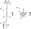
Figures 2A-2B are schematic illustrations of examples of multi-electrode lead systems with an IPG, which may include high impedance circuits or segments to provide a high impedance operation at selected RF frequencies according to embodiments of the present invention. -
Figures 3A and 3C are schematic diagrams that illustrate a lead system with electrodes and capacitors disposed therealong according to embodiments of the present invention.Figure 3A illustrates a linear system andFigure 3C illustrates a wound/coiled system. -
Figures 3B and 3D are schematic cross-sectional views of the systems shown inFigures 3A and 3B , respectively. -
Figure 4 is a schematic diagram that illustrates three conductors, three electrodes and capacitors disposed between conductor pairs according to embodiments of the present invention. -
Figures 5A and 5B are schematic diagrams of other multi-electrode high impedance leads according to embodiments of the present invention. -
Figure 6 is a schematic illustration of an implantable pulse generator with a high impedance operation according to embodiments of the present invention. -
Figures 7 and 8 are data charts/graphs of a coiled parallel inductor pair in a frequency range of between 1-150MHz. -
Figures 9 and 10 are data charts/graphs of a coiled parallel inductor similar to that shown with respect toFigures 7 and 8 , but modified with capacitors to provide higher impedance according to embodiments of the present invention. -
Figure 11 is a schematic illustration of the parallel inductors and capacitors used to provide the data ofFigures 9 and 10 according to embodiments of the present invention. -
Figure 12 is a graph of a sample loss of an open circuit for a frequency range of about 1- 150 MHz. -
Figure 13A is a schematic illustration of an electrode lead system illustrating an high-impedance surface shield, which may be used in an embodiment of the invention. -
Figure 13B depicts a lead system shown inFigure 13A illustrating shielding and conductor configurations, which may be used in an embodiment of the invention. -
Figure 13C is a cross-sectional view of the lead system shown inFigures 13A and13B . -
Figure 14 is a schematic illustration of a lead system with RF chokes that may be combined with one or more of the high impedance configurations shown and/or described herein according to embodiments of the present invention. -
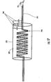
Figure 15A is a schematic illustration of an RF trap that can be used to form a high impedance segment on a lead but is not configured in accordance with the invention. -
Figure 15B is a schematic illustration of the RF trap shown inFigure 15A with the addition of a capacitor connecting the shield and the conductor. -
Figure 15C is a schematic illustration of the RF trap shown inFigure 15B illustrating that the RF trap may also include stray capacitance with a discrete capacitor. -
Figure 16 is a schematic illustration of a long lead with a plurality of axially spaced apart RF traps along a length of a conductor or lead which is not configured in accordance with the invention. -
Figure 17 is a schematic illustration of a lead system with RF traps having co-wound conductors in a common shield and does not form part of the present invention. -
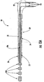
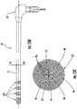
Figure 18A is a partial cutaway side view of a multi-lead system with an RF trap having co-wound conductors/filars and does not form part of the present invention. -
Figure 18B is a cross-section view taken along lines 18B-18B inFigure 18A . -
Figure 18C is a schematic line illustration of the embodiment shown inFigure 18A . -
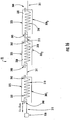
Figure 19A is a partial cutaway side view of a multi-lead system with an RF trap having co-wound conductors/filars with capacitors connecting the respective leads to the conductive shield at two locations and does not form part of the present invention. -
Figure 19B is a cross-section view taken along lines 19B-19B inFigure 19A . -
Figure 19C is a schematic line illustration of the embodiment shown inFigure 19A . -
Figure 20A is a partial cutaway side view of a multi-lead system with an RF trap having co-wound conductors/filars with less than all the leads/conductors in electrical contact with the shield and does not form part of the present invention. -
Figure 20B is a cross-section view taken along lines 20B-20B inFigure 20A . -
Figure 21A is a partial cutaway side view of a system with an RF trap having conductors coiled both separately and co-wound and does not form part of the present invention. -
Figure 21B is a cross-section view taken along lines 21B-21B inFigure 21A . -
Figure 21C is a schematic line illustration of the examples shown inFigure 21A . -
Figure 22 is a graph of impedance (Ohms) versus frequency (MHz) for the example shown inFigures 21A and 21B . - The present invention will now be described more fully hereinafter with reference to the accompanying drawings, in which embodiments of the invention are shown. This invention may, however, be embodied in many different forms and should not be construed as limited to the embodiments set forth herein; rather, these embodiments are provided so that this disclosure will be thorough and complete, and will fully convey the scope of the invention to those skilled in the art. It will be appreciated that although discussed with respect to a certain embodiment, features or operation of one lead system embodiment can apply to others.
- In the drawings, the thickness of lines, layers, features, components and/or regions may be exaggerated for clarity and broken lines illustrate optional features or operations, unless specified otherwise. In addition, the sequence of operations (or steps) is not limited to the order presented in the claims unless specifically indicated otherwise. It will be understood that when a feature, such as a layer, region or substrate, is referred to as being "on" another feature or element, it can be directly on the other element or intervening elements may also be present. In contrast, when an element is referred to as being "directly on" another feature or element, there are no intervening elements present. It will also be understood that, when a feature or element is referred to as being "connected" or "coupled" to another feature or element, it can be directly connected to the other element or intervening elements may be present. In contrast, when a feature or element is referred to as being "directly connected" or "directly coupled" to another element, there are no intervening elements present. Although described or shown with respect to one embodiment, the features so described or shown can apply to other embodiments.
- Unless otherwise defined, all terms (including technical and scientific terms) used herein have the same meaning as commonly understood by one of ordinary skill in the art to which this invention belongs. It will be further understood that terms, such as those defined in commonly used dictionaries, should be interpreted as having a meaning that is consistent with their meaning in the context of the relevant art and this specification and should not be interpreted in an idealized or overly formal sense unless expressly so defined herein.
- The term "high radiofrequency" or "high RF" refers to RF frequencies that are at or above about 1 MHz, and includes radiofrequencies in the range of about 1MHz to about 256 MHz. Embodiments of the present invention configure devices so as to have high impedance circuit segments or a high impedance circuit at high RF and low impedance circuit segments or circuit at DC or low frequency (at a kHz or less frequency or frequency range), i.e., at frequencies used for treatment such as stimulation or ablation. For example, for 1.5T, 3.0T and 6.0T systems, the respective frequencies are 64 MHz, 128 MHz and 256 MHz. The frequencies of the different MRI systems are well known to those of skill in the art. The devices can be configured to have high impedance at several of the radiofrequencies associated with high-field magnet MRI systems, such as systems with magnets above about 1.0T, such as about 1.0T, 1.5T, 2.0T, 3.0T, 4.0T, 5.0T, 6.0T and 9.0T, typically between about 1T to 15T.
- The term "high impedance" means an impedance sufficiently high to inhibit, block or eliminate flow of RF-induced current at a target frequency range(s). The impedance has an associated resistance and reactance as is well known to those of skill in the art. Some embodiments provide an impedance of at least about 300 Ohms, typically between about 400 Ohms to about 600 Ohms, such as between about 450 Ohms to about 500 Ohms, while other embodiments provide an impedance of between about 500 Ohms to about 1000 Ohms. Embodiments of the invention configure lead systems that provide sufficiently high-impedance at frequencies associated with a plurality of different conventional and future magnetic field strengths of MRI systems, such as at least two of 1.5T, 2.0T, 2.5T, 3.0T, 9.0T, and the like, allow for safe use in those environments (future and reverse standard MRI system compatibility).
- The term "tuned" means that a parallel resonant circuit with inductive and capacitive characteristics defined by certain components and configurations has a high impedance at one or more target frequencies, typically including one or more MRI operating frequencies.
- The term "coiled segment" refers to a conductive lead (trace, wire or filar) that has a coiled configuration. The term "co-wound segments" means that the affected leads, conductors, wires and/or filars can be substantially concentrically coiled at different radii, one above the other, or concentrically coiled closely spaced at substantially the same diameter. The term "co-wound" is used to describe structure and is not limiting to how the structure is formed (i.e., the coiled segments are not required to be wound concurrently or together, but may be so formed). The terms "conductive element", "conductive lead" and "conductors" are used interchangeably and refer to a conductive path that connects target components (such as, for example, a stimulation source and an electrode) and can include one or combinations of a metallic trace, a wire, a flex circuit, a filar(s), or other conductive configuration. As such, the conductors or conductive elements include long linear and/or non-linear conductors that can be formed with one or more of discrete wires, flex circuits, filars (bi, quadra or other winding), or by plating, etching, deposition, or other fabrication methods for forming conductive electrical paths.
- Embodiments of the present invention can be configured for any desired internal region of the body or object. The object can be any object, and may be particularly suitable for animal and/or human subjects. Some embodiments can be sized and configured for brain stimulation, typically deep brain stimulation. Some embodiments can be configured to stimulate a desired region of the sympathetic nerve chain and/or the spinal cord. Some lead or implantable devices can be configured for cardiac intervention. Other embodiments may be directed to other anatomical structures, organs or features including deep tissue, lumens, and the like. For example, the systems of the present invention may be configured for treatment of gastrointestinal, urinary, or other body regions. Some embodiments provide devices configured for intraluminal or intratissue penetration. Some embodiments provide devices for acute or chronic implantation.
-
- Generally stated, the extent to which the lead system or the long conductor couples with the external RF is a function of length of the lead system or the conductor, the insulation thickness over it and its arrangement in the RF field e.g. looping, etc. Typically, lengths shorter than quarter wavelength (at the applied RF frequency) do not couple with the external RF fields, displaying reduced RF deposition and lower local temperature rise in tissue adjacent to them. Also, typically, increasing the insulation thickness can reduce the coupling and RF deposition in the adjacent tissue.
- Long wires, conductors and lead systems couple to external RF to different extents at different frequencies. The extent of RF deposition in the tissue depends on the extent of resonation, i.e., the coupling at that frequency. Linear conductors/wires act as linear antennas. Lead systems which have more than one long conductor act as linear antennas, where each individual conductor acts as an antenna and two or more conductors in combination with each other act as antennas too. This creates a RF coupling pattern having the lead system couple at multiple/different frequencies. DBS and cardiac pacing leads may comprise about 8 (and may include more or less) long conductors and electrodes. In particular embodiments, one, some or all of the conductors can act as antennas individually and in combination with each other.
- Internal and external imaging coils used in MRI can be decoupled during RF transmit by the scanner. This can inhibit local heat deposition in the tissue adjacent to the coils. The decoupling mechanism can create a high impedance circuit so that these coils do not couple with the transmitted RF, thus eliminating any tissue damage. See, Yoda K., Decoupling technique for transmit coils in NMR spectroscopy and imaging,. NMR Biomed 1990;3(1):27-30; and Buchli et al., Increased RF power absorption in MR imaging due to RF coupling between body coil and surface coil, Magn Reson Med 1989; 9(1):105-112.
- Similarly, standing wave formation on long coaxial cables may be attenuated by incorporating balun circuits or RF chokes at various locations on the shield of coaxial cables. See,
Atalar et al., U.S. Patent No. 6,284,971 , entitled, Enhanced Safety Coaxial Cables. - See also, Ladd et al., Reduction of resonant RF heating in intravascular catheters using coaxial chokes, Magn Reson Med 2000; 43(4): 615-619. See also,
WO 2006/031317, filed August 9, 2005 , entitled, Implantable MRI Compatible Stimulation Leads and Antennas and Related Systems and Methods. - Generally stated, this application describes incorporating RF chokes on DBS and CP lead systems.
- Shielding linear conductors can inhibit RF deposition on them. This shielding can be continuous, discontinuous, or may be achieved by multiple methods, to list a few, e.g., insulating conductors with polymers filled with conducting metals doped for conductivity.
- Referring now to the figures, in some embodiments as shown in
Figures 1A and 1B , a highimpedance lead assembly 20 can employ at least oneconductor 20c, shown as twoconductors Figure 1B ) and/or reside parallel (Figure 1A ) to each other, or be configured with combinations of both, and that are operational over a relatively wide range of frequencies. Theselong conductors 20c can have a metal core and are typically insulated from each other along their length and may be surrounded by apolymeric dielectric 20i. At intermediate locations, the twoconductors capacitors 3. The combination of the length of theconductors 1 and 2 (which can also form inductors) and thecapacitors 3 is configured to create a high impedance circuit(s). This circuit is configured so that it does not tune to a target range of RF frequencies, including for example, frequencies ranging from about 1 MHz to 250 MHz, creating high impedance circuit segments, thus reducing the extent of coupling in this frequency range. In operation, the circuit has high impedance to high RF, but has low resistance to DC, or low frequency RF (KHz), which is the stimulation frequency. This principle may be applied to designing RF/MRI-safe devices and/or lead systems for CP leads, DBS leads, spinal cord stimulation leads, etc. - The
capacitors 3 can be regularly spaced or irregularly spaced. Thecapacitors 3 may have the same or different capacitance from each other. - Lead
systems 20 can comprise a plurality of electrodes and conductors, such as between about 2 to about 10 conductors, typically at least about 4. In some embodiments, the lead systems can include about 8 conductors. The conductor axial lengths (linear and/or coiled) can range from about 10 to 200 cm, with a thin insulator layer on the conductors and with a polymeric dielectric insulator layer over it. - Design of conventional known lead systems with multiple electrodes 1001-1004 and
conductors 20c are shown inFigures 2A-2B . See also,U.S. Patent Application Publication No. 2005/0222647 . - Referring to
Figures 3A and 3B , at a distal end portion of thelead system 20, theconductors 20c can be connected toelectrodes conductors 20c run along the length of the lead system and are terminated by connecting toelectrodes - In some embodiments, as shown in
Figures 3A , two (straight/linear)parallel conductors 8 and 9 are connected to each other at intermediate locations bycapacitors 10 along the length of the lead system to form high impedance sections. Thecapacitors 10 can be semiconductor-based discrete products or can be otherwise provided, such as using coatings of metal oxides, e.g. tantalum oxide, and the like at discrete certain locations so as to connect the twoconductors 8, 9 at desired locations. -
Figure 3C , similar toFigure 3A , illustrates two parallel conductors but aswound conductors capacitors 3 in communication therewith and tworespective electrodes - In embodiments that employ more than two
conductors 20c, more than one high impedance circuit can be formed with different conductor pairs. For example, as shown inFigure 4 , where there are threeelectrodes conductors 20c, labeled as elements, 8, 9, and 12,respective capacitors 10 can be disposed between conductor pairs (8, 12 or 12, 9, as shown). Also, oneconductor 20c may be used in combination with two conductors to form two separate high impedance circuits. - In some embodiments, the
lead systems 20 can conduct DC or a low frequency AC (KHz), typical of stimulation current. Theconductors 20c may be made of any suitable (MRI compatible and/or non-ferromagnetic) conducting material and/or metal, e.g., Nitinol, Cobalt-Chromium alloy, MP35N alloy, gold, silver, platinum, platinum-iridium alloy, stainless steel, copper and other non-ferromagnetic materials, which will not cause a susceptibility artifact in MRI or magnetically react to the magnetic field in an MRI scanner environment. DC conductivity is a bulk phenomenon and RF conductivity is a skin depth phenomenon. The RF conductivity of the lead system may be reduced by using composite wire (a conductor or wire formed of a combination of different conductive materials) such as by using a resistive metal such as tungsten, MP35N or Nitinol wire on the outside and with a conductive core formed of gold, silver or copper or other metals. This may reduce RF transmission along the length of the lead system, thus reducing the amount of RF that may be deposited in the tissue. Further, these leads made of composite wires (with a resistive outer layer and conductive core) can have an insulator coating on the outer surface and may be connected by capacitors to form high impedance RF circuits along the length of the lead system as described above with respect toFigures 1-4 . -
Figures 5A and 5B illustrate lead systems formed with high impedance segments of two or moreinsulated conductors 20c with any single conductor and/or a composite conductor structure having apolymeric layer 13 over them. As shown, the leads may be further shielded by a polymeric dielectric material with metal orconductive particulates 13c (Figure 5A ) dispersed therein to shield/deflect external RF. In some embodiments, the polymeric dielectric orinsulation 13c over theconductors 20c may be filled/dispersed or mixed with another high dielectric constant material, e.g., titanium dioxide, etc., to regulate the impedance between (two or more) conductors. - Also, or alternatively, conductive shielding 325 as a continuous or discontinuous conductor layer (braided, coated, etc) may be applied over the
conductors 20c of the lead system as shown inFigure 5B . An insulatingpolymeric material 13 may reside between theconductors shield 325. A polymerouter layer 21 may encase thelead system 20. - In some embodiments, as shown in
Figure 14 , RF chokes 64rf, as described inWO 2006/031317 , filed August 9, 2005 , entitled, Implantable MRI Compatible Stimulation Leads and Antennas and Related Systems and Methods, may be incorporated over these high impedance segments or leads to further prevent formation of standing RF waves. - In some embodiments, as shown in
Figure 6 , anIPG 102 can have alead system 20 withmultiple conductors 20c that connectdistal electrodes 100. The IPG may optionally include adecoupling circuit 200 which can be incorporated in an implanted housing of theIPG 102 and/or in a connector or portion of the IPG lead assembly (a connector or end portion of the lead assembly rather than the housing itself). TheIPG 102 can include apower source 102b, such as a battery. Thecircuit 200 can be in communication with adigital controller 121 that can programmatically activate the circuit 200 (and/or deactivate the circuit 200). Thelead system 20 may optionally be arranged as an antenna described earlier with two or more capacitor sets per antenna. - Implantable IPGs can be used with other lead system configurations which do not form part of the present invention
(see, e.g.,Figures 15-22 ). The lead system can be transformed to a high impedance lead (and/or antenna) by activating thedecoupling circuit 200 to a short circuit, before an MRI scan or exposure to external RF. This activation can create a high impedance circuit with the capacitors and inductor assembly in the lead body making the lead electrically invisible to the external RF thus reducing coupling with the RF. The decoupling may comprise a single or multiple circuits tuned to different frequencies and can be programmed to be activated accordingly. The activation and/or adjustment to different RF frequency and/or deactivation can be carried out by a wireless command sent to the IPG. The activation may be carried out internally (automatically) in response to detection of an RF signal. - Some
lead systems 20 of the instant invention can be configured so that one or more conductors behave as inductors or comprise inductive components. The inductors can be provided by coiled conductor (wire) segments, flexible dielectric substrates, or other inductor configurations. In some embodiments, at high frequency, capacitors can act as shorts and may not, by themselves, give sufficiently high impedance. Thus, thelead systems 20 can include inductors that cooperate with the capacitors. The leads or conductors of the systems can have high impedance at high frequency and low impedance at low frequency by configuring the conductors (wires/leads) to behave as inductors. - In some embodiments, at least one
conductor 20c of thelead system 20 comprises a wound coil segment of the at least one conductor to define a coil inductor. In particular embodiments, the coil inductor may be wound to encase other another conductor(s) of the lead system. The coil inductor can be formed as substantially an entire length of a first conductor or as a smaller portion of the conductor. The capacitors can connect sections of the coil inductor and a second conductor. -
Figures 7 and 8 are graphs of data associated with a 12 cm long coiled inductor pair open at both ends when loaded in saline. The conductors are 32 AWG magnet wire closely wound on a 0.020 inch mandrel. The graph shows an X-axis frequency sweep from 1.0 to 150 MHz. The two-conductor assembly tunes at different frequencies to different extents as represented by the arrows inFigure 8 . -
Figures 9 and 10 illustrate the same parallel inductors as described above (Figures 7 and 8 ) with 0.5 pF capacitors placed at about 2.5 cm apart at 5 locations. The return loss is flatter and higher than -8 db for all frequencies. It is contemplated that this loss can be further reduced (closer to zero) in an optimized design. -
Figure 11 is a schematic diagram of the parallel inductors with theinductor coil 1 being the wider outside strip and theinductor coil 2 being the inner strip (slightly thinner). The 0.5 pF inductors (3, 4) are shown positioned between the twoinductors -
Figure 12 is a graph of a sample return loss of an open circuit for a frequency range of between about 1-150MHz. -
Figure 13A illustrates an example of an MRI/RF safe lead system with anIPG connector 22 and IPGelectrical connections 23, which system is not per se an embodiment of the present invention. As shown, the lead
system 20 includes a plurality ofelectrodes 100, respective conductors/wires 20c, aprimary shielding 33, a segmented secondary shielding 34, segments /inductors 35, and a segmentedtertiary shield 36. The segments/inductors 5 connect the secondary 34 andtertiary shield 36 to theprimary shield 33. Thelead system 20 and/or theconductors 20c of the lead system are shielded by one or more layers of shield arrangements as shown inFigure 13A . This creates a high impedance surface and inhibits RF coupling of the lead system and any formation and/or transmission of a standing wave. This may be defined as a "3-D RF band gap structure" 39 which is an RF open circuit, while being a DC (and/or potentially a low frequency AC) short circuit. This structure can include a thin, typically two-dimensional, pattern of capacitive and inductive elements, which act as miniature parallel resonant circuits which block RF propagation. - In some examples the
conductors 20c can be coiled individually or co-wound, or combinations of each. At one end portion, typically a proximal end portion of the segment, theconductors 20c can be selectively connected to the high impedance shield directly or indirectly in a capacitor which act as an RF open and low frequency (DC) open circuit. -
Figure 13B illustrates a side view of the device shown inFigure 13A .Figure 13C is a cross-sectional view. As shown, a polymer dielectric insulatingovercoating 21 can be applied to thelead system 20. As also shown, dielectric/insulation layers 46, 48, 40 may be disposed intermediate the shielding layers 33 (primary shield), 34 (segmented secondary shield), and 36 (segmented tertiary shield). Theconductors 20c extend toconnector 22 andelectrical connections 23 to the IPG or other stimulation, ablation or recording device. Capacitors 24 (Figure 13A ) are not required according to some examples , as the segmented shielding configurations and inductor lead configuration may provide suitable impedance at high frequency. It is emphasised that such examples do not form part of the present invention. -
Figure 14 illustrates an electrode arrangement with RF chokes 64rf that can be used with high impedance circuits/segments and configurations described and/or shown herein. Eachelectrode 100 is typically in communication with at least one of theinsulated conductors 20c. At the proximal end of thelead support body 20, theconductors 20c are connected to aconnector 22 withelectrical connections 23 so as to be connected to theimplantable signal generator 102 or to an external circuit, such as aninterface circuit 40 during MRI guided lead/cable placement. Thelead support body 20 need not be able to provide MRI signals (i.e., it can optionally be configured with an MRI receive antenna). Theseinsulated conductors 20c are typically covered with a polymeric insulator sleeve 61 and a conducting material is cylindrically layered to form thefirst shielding layer 62 over the insulator. This shielding 62 may be terminated proximal to theelectrodes 100 and, in this embodiment, may not be in electrical contact with the conductors and/or the electrodes. A second insulator/polymeric/dielectric layer 63 further insulates this shielding 62 to form multi-core coaxial type cable system, with an impedance that is typically between about 10-100 ohms. The RF chokes 64rf can be integrated or built into the shielding 64 in the form of a second shielding, which is not continuous and has multiple sections each λ/4 or less in length. As shown inFigure 14 , at the proximal end, each section orsegment 64s is connected to theprimary shielding 62, and the distal end may not be electrically connected to theprimary shielding 62, or is connected with acapacitance 164 in between the primary and secondary shielding 62, 64, respectively. A top insulator/polymeric layer 65 can be used to insulate thebody 20b, except for the electrodes 25. - As shown by the axial arrow in
Figure 14 , the MRI active portion of theantenna 35 may extend between a location where theprimary shield 62 terminates and the first electrode 251. However,other antenna 35 configurations may also be used. As shown, the second shield layer 64 comprises a plurality of axially spaced apart RF chokes 64rf. The term "RF chokes" refers to a shielding layer configuration that provides an electrical length of less than or equal to λ/4 (from the perspective of external electromagnetic waves) to inhibit the formation and/or propagation of RF induced current or standing waves in an AC (alternating current, e.g., diathermy applications) or RF exposure environment. The physical length that provides the electrical wavelength may vary depending on the materials used in fabricating the catheter or lead system support body (such as dielectric constant) and the magnetic field in which it is used. In some embodiments, thelead system 20 has a physical length that is greater than 10 cm, typically between about 20 cm to about 150 cm. In some embodiments, the implantable lead segment 50 can also include RF chokes 64rf formed along target regions or along substantially the entire implantable length. In the embodiment shown inFigure 14 , the RF chokes 64rf comprise a plurality of disconnects of the shield 64 and/or discrete electrically isolated second shield segments. In other embodiments, the RF chokes 64rf can include a series of axially spaced apart Balun circuits or other suitable circuit configurations. See, e.g.,U.S. Patent No. 6,284,971 for additional description of RF inhibiting coaxial cable that can inhibit RF induced current. - As shown in
Figure 14 , the second shield layer 64 may be coupled to thefirst shielding layer 62 at opposing ends of thesegments 64s. As shown, one end (typically the proximal end portion) of the disconnectedsegment 64s is directly coupled to theshielding layer 62 and the other end (typically the distal end portion) is capacitively coupled to thefirst shielding layer 62. Eachsegment 64s may be configured to engage thefirst shield layer 62 in the same manner or in an opposing different electrical manner (not shown). -
Figures 15A-15B illustratelead systems 20 with at least onehigh impedance segment 300 with associated axially spaced apart proximal and distal portions, 330p, 300d, respectively. These lead systems are not configured in accordance with the present invention. Thehigh impedance segment 300 can be described as an RF trap that includes aconductor 20c being coiled to define aninductor 310 within aconductive shield 325 and with an insulator/dielectric material 330 between theinductor 310 andshield 325. Theconductor 20c can be in electrical communication with theconductive shield 325 at one end (shown inFigure 15A as theproximal end portion 300p) of thehigh impedance segment 300. - The implantable lead system can include multiple high impedance sections or
segments 300 along the length of the lead. The high impedance sections or segments are created by arranging the components of the medical device, i.e., the conductor, etc. as an RF trap. These high impedance RF traps inhibit the flow of induced RF current (at the frequency to which the RF trap is tuned) and prevent it from heating tissue adjacent to the electrodes, thus minimizing or preventing RF induced tissue damage. Since the physiological and stimulation signals are at low frequencies (KHz range), the RF trap allows the lower frequency signal(s) to go through, trapping only the higher frequencies of interest to which the traps are tuned. - As shown in
Figure 15A , theconductor 20c can be in electrical communication with the shield at the distal portion of thehigh impedance segment 300 via atuning capacitor 340. The high impedance segment 300 (e.g., RF trap) can be tuned to a MRI frequency. Thesegment 300 can also be configured so that theconductor 20c at the proximal end portion of thesegment 300p is connected to theshield 325 via acapacitor 360. Differenthigh impedance segments 300 may be tuned to different MRI frequencies (i.e., 64 MHz and 128 MHz or other standard operating frequencies of commercial MRI scanners). The impedance of thesegment 300 can be at least 400 Ohms, typically greater than about 450 Ohms. The at least onehigh impedance segment 300 can be placed at between about 0.1-12 cm from the electrode(s) 100. The lead 20c can be configured with astraight segment 311 that merges into thecoiled segment 310. - In operation, the
RF trap 300 with theshield 325,inductor 310 andtuning capacitor 340 form a high impedance parallel resonant circuit at the desired frequency to block RF currents along the conductor. The tuning capacitor can include one or more of a discrete capacitor 340 (Figure 15A ) and/or stray capacitance 350 (Figure 15B ) between theinductor 310 and theshield 325. -
Figure 15B illustrates that thehigh impedance segment 300 may includestray capacitance 350 that resides between theconductive shield 325 and theinductor 310 through the insulator/dielectric 330. Thestray capacitance 350 and/or thediscrete capacitor 340 can be used to tune the RF trap to a high-impedance at a desired frequency (range), typically between 1MHz to 250MHz. Anothercapacitor 360 may also be used at the opposing end of thesegment 300 to form an RF short (not shown). Thehigh impedance segment 300 can be tuned to achieve high impedance at desired frequencies by varying the length of the trap structure, thereby increasing or decreasing the total capacitance and inductance until the resonant condition is met at the desired frequency.Different segments 300 along alead length 20 can be tuned to a different (typically MHz) frequency. - As shown in
Figure 16 , which also does not form part of the present invention, aconductive lead 20c can include a plurality
ofhigh impedance segments 300 that can be positioned along the length of thelead system 20 at regular or irregular intervals, but typically so that the spacing provides an electrical length of less than about λ/4 therebetween. The RF traps 300 are placed less λ/4 apart, where λ is the wavelength in the medium of the operating frequency, to electrically break the long conductor into multiple sections. -
Figure 17 , which also does not form part of the present invention, illustrates that a plurality ofconductors
be co-wound (seeelement 310c) and reside within a commonflexible shield 325. Eachconductor shield 325 at a proximal portion thereof, directly or indirectly, such as using arespective capacitor 360 as shown. Thecapacitor 360 can provide an RF short. The high impedance segments 300 (RF traps) are placed less than a λ/4 apart from each other at the desired frequency. - When multiple high impedance segments 300 (using, for example RF traps) are incorporated over the length of a device such that the distance between two adjacent traps is less than one-quarter wavelength, this effectively breaks the long conductor into multiple sections, each shorter than a quarter wavelength. The RF current induced on a conductor is a function of length of the conductor at the RF frequency, and when the conductor is shorter than a quarter wavelength, the RF current induced is not large enough and may not cause undue RF deposition RF induced-treating of the tissue.
- For a bare copper wire λ/4 in a physiological medium, the length has been measured at about ∼ 8 cm at 64 MHz (1.5T) and 4 cm at 128 MHz (3T). For implantable leads where the conductors are insulated with a polymeric layer of about or > 0.001 inches thick, and have an electrode exposed to tissue, the temperature change in the tissue adjacent to the electrode due to RF deposition is measured to be less than 1°C at length less than 15 cm at 1.5T (64 MHz frequency). When a high impedance segment or section 300 (using one or more RF traps) is incorporated in the length of the
conductor 20c, thesection 300 can be positioned such that the distal end of thetrap 300d is less than 15 cm from one or more of theelectrodes 100 and the impedance can be greater than about 450 Ohms at a target MRI frequency, in order to reduce RF deposition induced heating at the electrodes (less than 1°C). Thus, in some embodiments,multiple segments 300 with impedance of about or greater than 450 Ohms (at 64 MHz) are placed at distances less than 15 cm apart on a long conductor, which can make theconductor 20c safe to use in MRI at 1.5T. Similarly if thesesegments 300 have an impedance of about or greater than 450 Ohms at 128 MHz and are placed <10 cm apart (Length ∼ λ/4 at 128 MHz, or 3T MRI frequency), it can effectively reduce the extent of heating at the electrode in a 3T MRI environment. - Different designs of
high impedance segments 300 along the length of the leads for multi-conductor lead systems with electrodes are described herein. Suchhigh impedance segments 300 can be placed along the length (less than λ/4 length apart from each other) of thelead 20 to reduce RF deposition at theelectrodes 100 and inhibit undue tissue damage. -
Figures 18A-18C , which do not form part of the present invention, illustrate ahigh impedance segment 300 with four
co-wound conductors/filars 20c1-20c4 and ashield 325 placed over theco-wound conductors 310c which is connected to theconductors 20c1-20c4 at the proximal end of thetrap 300p viarespective capacitors 360. Thecapacitor 360 can have a relatively large capacitance sufficient to act as an RF short and a DC and low frequency (Hz, kHz) open circuit. Theconnection 370 can be via a metallic trace, small wire or other connection from alinear segment 311 of theconductor 20c to theshield 325 as theconductor 20c merges into acoiled segment 310. A polymericouter layer 21 can be provided over theshield 325. Thelead system 20 can be a flexible lead system and thedielectric material 330 can be provided as a flexible material. - As shown in
Figures 18A and 18B , for a lead 20 comprising one or more insulated filars/conductors 20c, the filars/conductors 20c can have astraight section 311 followed by acoiled section 310 that forms the inductor. Thecoiled section 310 may be co-wound with another filar/conductor. A dielectric/insulator 330 can be placed on thecoiled section 310 and ashield 325 can be placed on the co-wound conductors separated by the dielectric 330 between them. As shown, at the proximal end portion of thecoil 310, theshield 325 is connected (via trace or wire 370) to eachconductor 20c1-20c4 by acapacitor 360 which acts as an RF short at high frequencies and a DC and low frequency open circuit. - Although the
tuning capacitor 340 is shown in various embodiments at a distal portion of thesegment 300d and the RF short and low frequencyopen circuit capacitor 360 is shown at theproximal portion 300p, the reverse orientation may also be used. Also, alternating or different orientations can be used along a length of thelead system 20. - The length of the shielded
co-wound segment 300 is such that a high impedance (typically greater than about 450 Ohms) is created at the distal end of thesegment 300d between theshield 325 and the conductor(s) 20c at one or more frequencies. Typically, at least one frequency is an MRI frequency, such as about 64 MHz. Thishigh impedance segment 300 created by shielded coiled conductors/inductors, with theshield 325 electrically connected to theconductors 20c at the proximal end portion of thesegment 300p, inhibits RF current from flowing along the length of thelead 20. One or more of such segments 300s, tuned to one or more RF frequencies, may be incorporated along the length of the lead. The length of eachsegment 300 may be between about 0.1-200 cm, typically between about 1-200 cm, and more typically between about 6 cm to about 15 cm. -
Figures 18A, 18B ,18C ,19A and 19B , none of which form part of the present invention, illustrate a high impedance segment
300 with fourconductors 20c1-20c4. Theconductors 20c1-20c4 may comprise filars that have astraight section 311 and acoiled section 310. Thestraight section 311 may be between about 0-15 cm long and a respective coiled section may be between about 1-150 cm long. An insulator/dielectric material 330 with dielectric constant >1 separates theconductors 20c (coiled and straight sections, 310, 311) and theshield 325 is placed over theinsulated conductors 20c1-20c4. Thehigh impedance section 300 may be between about 1-150 cm long. - In the embodiments shown in both
Figures 18A and19A , at the proximal end of thehigh impedance section 300p, theshield 325 is connected to theconductors 20c viacapacitors 360, typically having a value between about 100pF to 10000 µF, using a trace orthin wire 370 to facilitate the connection. Thiscapacitor 360 creates an RF short at high frequencies and a low frequency and DC open circuit and inhibits the stimulation current from getting shorted in theshield 325. The diameter of thelead system 20 can be between about 0.10-19 mm, typically between about 0.5-6 mm, and can be varying in different sections of the lead. Thelead 20 may be substantially flat, elliptical, circular, rectangular, or square in cross-sectional shape. -
Figures 19A-19C illustrate alead system 20 with at least onehigh impedance segment 300 similar to that shown inFigures 18A and 18B , but with theconductors 20c connected to theshield 325 viacapacitors proximal end portion high impedance segment 300. At one end, for example, the proximal end as shown, thecapacitances 360 are large, representing an RF short circuit at high frequency but low frequency open circuit at low frequencies. At the other end, thecapacitances 340 are adjusted so that the inductance-shield-capacitance combination forms a high impedance circuit. The inductance and the capacitance are adjusted such that thehigh impedance segment 300 is tuned to a high impedance at desired frequency or frequencies, where one of these frequencies is an MRI frequency. This design can control the length of the segment 300 (RF trap) to a desired length, such as, for example, less than λ/4 (< 10 cm at the desired frequency in physiological medium). Ahigh impedance segment 300 is tuned to a desired frequency by adjusting the values of the parallel resonant circuit created by the RF trap capacitors 360 (and 350 shown inFigure 15B , where used) and the inductance of thecoiled filars 310. This configuration can adjust the length of the segment 300 (RF trap) and the impedance at a RF frequency of interest. One ormore segments 300 tuned to one or more MRI frequencies can be placed along the length of thelead 20. - Again, it is noted that in some embodiments, at one end, either the distal or proximal end, the capacitances of the capacitor(s) 360 are sufficiently large to represent an RF short at high frequency but a low frequency open circuit at low frequency. At the opposing other end, the
capacitances 340 are adjusted (tuned) so that the inductance-shield-capacitance combination forms the high impedance. -
Figures 20A and 20B , which also do not form part of the present invention, show ahigh impedance segment 300 with an RF
trap with a single one of the four (20c1-20c2)conductors 20c connected to theshield 325 at a proximal portion of thesegment 300p.Multiple segments 300 with RF traps similar to the one shown can be placed along the length of thelead 20 and a single different one or pairs or other combinations of theconductors 20c can be serially connected to theshield 325 per different RF trap location, so that eachconductor 20c has been connected to theshield 325 at least once before it reaches anelectrode 100. - The
high impedance segment 300, shown inFigures 20A-20C , includes a plurality ofco-wound conductors 20c1-20c2, wherein only one conductor is connected to theshield 325 at a time. Theshield 325 is connected to only one conductor per segment 300 (via a capacitor or directly). In a long lead, the series ofsegments 300 can be incorporated along the length of thelead 20 and eachsegment 300 can be designed such that the eachconductor 20c is connected to theshield 325 at least once over the length of the lead. In this lead design, the number ofsegments 300 along the length of thelead 20 can at least equal the number ofconductors 20c in the lead. -
Figures 21A-21C , which also do not form part of the present invention, illustrate ahigh impedance segment 300 with an RF
trap having conductors 20c coiled in two different manners: aco-wound segment 375 and a discretely coiled segment 380 (shown as four discrete segments 3801, 3802, 3803, 3804, one for eachconductor 20c1-20c4 ) under thesame shield 325. Thesegment 375 can be described as having a common co-wound configuration at a common axially extending location. However, one or more of theconductors 20c can be co-wound with one or more other conductors for substantially the entire length of thesegment 300 without having an individual or discrete coiled segment 380 in the high impedance segment 300 (i.e., can be co-wound with less than all of the conductors) at a portion of the length of thesegment 300 - The
shield 325 can be connected to at least one of theconductors 20c at theproximal end 300d directly or indirectly. As shown, aconnection 370 connects eachconductor 20c1-20c4 viarespective capacitors 360 to theshield 325. Although not shown, one or more of theconductors 20c may be connected to theshield 325 at a distal end of thesegment 300 via acapacitor 340. - The length of the individual coiled inductors may not be the same on all conductors and is a function of location with respect to other inductors in the
segment 300 of the RF trap. This arrangement can be used to create a high impedance at the distal end of the RF trap at one or more frequencies (both in MHz) as shown inFigure 22 . One or both of these frequencies is an MRI frequency. - The length of each individual coiled section 380 and
co-wound section 375 can be 0.1-5.0 cm depending on the diameter of the coiled inductor. The spacing between the individually coiled inductors 3801-3804 may be between about 0.1-2 cm. This configuration allows a high impedance segment to generate high impedance at a plurality of MHz frequencies, where at least one frequency is an MRI frequency as shown inFigure 22 . - In some embodiments, the conductors or other metallic components of the
lead systems 20 may include one or more of: Nitinol, Cobalt- Chromium alloy, MP35N alloy, gold, silver, copper, platinum, platinum-iridium alloy, and other non ferromagnetic materials which will not cause a susceptibility artifact in MRI or magnetically respond to a high field magnet associated with MRI scanners. - Polymeric components can comprise polyurethane, fluorinated ethylene copolymer (FEP, ETFE), PTFE (Teflon), Nylon, PEBAX, polyethylene, polypropylene, and the like. As discussed above, the polymer may be filled with a metallic powder or other fillers.
- The conductive shield material may be metallic or conductive non-metallic and may be braided, coiled or deposited over the
insulation layer 330 over theinductors 325. The capacitors 340,360 may comprise semiconductor chip capacitors. Although the exemplary materials are described with respect to embodiments described inFigures 15-22 , the same materials can be used with respect to other embodiments described herein. -
Figure 22 is a graph of impedance vs. frequency characteristics for thelead system 20 shown inFigures 21A and 21B . High impedance is observed at two frequencies. The impedance and frequency are a function of individual inductors and spacing between them. It is contemplated that the design can be configured to generate high impedance at a plurality of frequencies in the MHz range, allowing the lead system or device to be compatible with two or more different field strength MRI scanners (i.e., 1.5T and at least one other higher field system such as a 2.0T, 3.0T or even 9.0T system). - Examples can be configured to reduce heating at an end of the
shield 325 at thedistal portion 300d of the high impedance segment (RF trap) 300. The impedance of the RF trap is a function of the inductance of the inductor and the capacitance between the shielded inductor. To achieve impedance > 450 Ohms on an inductor of small diameter (typically less than about 1 mm) with more than oneconductor 20c co-wound, the length of the segment 300 (RF trap) may sometimes exceed 15 cm. Thelead system 20 can be configured with supplementalhigh impedance segments 300 similar to those described herein with respect to the conductors, or RF chokes, balun circuits and the like may be incorporated on or in theshield 325. Alternatively, or additionally, discrete tubular resistors may be incorporated on or into theshield 325 to inhibit RF deposition at the distal ends of the shield. Alternatively or additionally, a thickness of the outer insulator/polymer layer 21 can be increased to reduce the likelihood of undue RF deposition at the distal end of the shield. - In the drawings an sspecification, there have been disclosed not only embodiments of the invention, but also alternative examles which do not form part of the present invention. Although specific terms are employed, they are used in a generic and descriptive sense only and not for purposes of limitation, the scope of the invention being set forth in the following claims. Thus, the foregoing is not to be construed as limiting the present invention. Although a few exemplary embodiments of this invention have been described, those skilled in the art will readily appreciate that many modifications are possible in the exemplary embodiments without materially departing from the novel teachings and advantages of this invention. Accordingly, all such modifications are intended to be included within the scope of this invention as defined in the claims.
- Therefore, it is to be understood that the foregoing is not to be construed as limited to the specific embodiments disclosed, and that modifications to the disclosed embodiments, as well as other embodiments, are intended to be included within the scope of the appended claims. The invention is defined by the following claims.
Claims (18)
- An MRI/RF compatible medical device, comprising:an implantable lead system (20) elongate lead having at least a first and a second electrode (1001, 1002), each associated with a respective first and second axially extending conductor (1, 2), wherein, at each of a plurality of intermediate locations along at least a major portion of the length of the lead system (20), at least one of a plurality of spaced apart capacitors (3) is disposed between the first and second axially extending conductors (1, 2) to define a plurality of high impedance circuit segments, each high impedance circuit segment comprising at least a portion of the first axially extending conductor (1), at least a portion of the second axially extending conductor (2), and at least one of the plurality of spaced apart capacitors (3), wherein each of the plurality of high impedance circuit segments is configured as an RF trap that inhibits flow of induced RF current at a target range of high frequencies to inhibit heating tissue adjacent to the electrodes (1001, 1002) of the lead system (20), wherein high frequencies are frequencies at or above 1 MHz, whereby the lead system (20) has a high impedance at the target range of high frequencies and a low impedance at low frequencies.
- A device according to claim 1, wherein the high impedance circuit segments are configured to reduce or eliminate electronic coupling of the lead system (20) to external RF.
- A device according to claim 1 or 2, wherein the high impedance circuit segments are configured to reduce or eliminate transmission of induced RF along the length of the lead system (20).
- A device according to claim 2 or 3, wherein the lead system (20) comprises three axially spaced apart electrodes (1001, 1002, 1003) and a respective first, second and third conductor (8, 9, 12), and wherein some of the capacitors (10) are arranged to extend between the first and second conductors (8, 12) and others (10) are arranged to extend between the second and third conductors (12, 9).
- A device according to claim 4, wherein the capacitors (10) between the first and second conductors (8, 12) are axially offset from the capacitors (10) between the second and third conductors (12, 9).
- A device according to any preceding claim, wherein at least one of the first and second conductors (1, 2) defines an inductor that is in electrical communication with at least two of the capacitors (10).
- A device according to any preceding claim, wherein the spaced apart capacitors (10) are substantially regularly spaced apart axially.
- A device according to any one of claims 1 to 6, wherein at least some of the spaced apart capacitors (10) are axially spaced apart at irregular intervals from the others over the length of the lead system (20).
- A device according to any preceding claim, wherein the components of the lead system (20) are formed from non-magnetic materials.
- A device according to any preceding claim, wherein the high impedance circuit segments are configured to inhibit RF transmission along the lead system (20) during exposure to RF associated with a high-field magnet MRI system.
- A device according to claim 10, wherein the high impedance circuit segments include
inductors (310) distributed along at least a major portion of a length of at least one of the conductors (1, 2). - A device according to claim 11, wherein the inductors (310) comprise a coil inductor (310) defined by a wound coil segment of the at least one conductor (1, 2).
- A device according to claim 12, wherein the coil inductor (310) is wound to encase other conductors (1, 2) of the lead system (20).
- A device according to claim 12, wherein the coil inductor (310) is substantially an entire length of the at least first conductor (1), and wherein the spaced capacitors (10) connect segments of the coil and the second conductor (2).
- A device according to any one of claims 11 to 14, wherein the first and second conductors (1, 2) have a respective length, and wherein portions of the length of the first and second conductors (1, 2) disposed axially between the spaced apart capacitors (10) comprise inductors.
- A device according to any one of claims 11 to 15, wherein the values of the capacitances and the inductors associated with the lead system (20) define a high impedance over the RF range of between about 1-150 MHz and a low impedance at frequencies less than about 50 kHz.
- A device according to any preceding claim, further comprising an electrically insulating biocompatible coating (21) disposed over an external surface of the lead system (20).
- A device according to claim 1, further comprising a high impedance band gap surface formed along at least a major length of the lead system (20).
Applications Claiming Priority (2)
| Application Number | Priority Date | Filing Date | Title |
|---|---|---|---|
| US72902005P | 2005-10-21 | 2005-10-21 | |
| PCT/US2006/041109 WO2007047966A2 (en) | 2005-10-21 | 2006-10-20 | Mri-safe high impedance lead systems |
Publications (3)
| Publication Number | Publication Date |
|---|---|
| EP1933933A2 EP1933933A2 (en) | 2008-06-25 |
| EP1933933A4 EP1933933A4 (en) | 2009-07-15 |
| EP1933933B1 true EP1933933B1 (en) | 2018-11-28 |
Family
ID=37963336
Family Applications (1)
| Application Number | Title | Priority Date | Filing Date |
|---|---|---|---|
| EP06817232.9A Active EP1933933B1 (en) | 2005-10-21 | 2006-10-20 | Mri-safe high impedance lead systems |
Country Status (5)
| Country | Link |
|---|---|
| US (3) | US8055351B2 (en) |
| EP (1) | EP1933933B1 (en) |
| AU (1) | AU2006304775B2 (en) |
| CA (1) | CA2623453C (en) |
| WO (1) | WO2007047966A2 (en) |
Families Citing this family (153)
| Publication number | Priority date | Publication date | Assignee | Title |
|---|---|---|---|---|
| US8244370B2 (en) | 2001-04-13 | 2012-08-14 | Greatbatch Ltd. | Band stop filter employing a capacitor and an inductor tank circuit to enhance MRI compatibility of active medical devices |
| US8256430B2 (en) | 2001-06-15 | 2012-09-04 | Monteris Medical, Inc. | Hyperthermia treatment and probe therefor |
| CA2482202C (en) | 2001-04-13 | 2012-07-03 | Surgi-Vision, Inc. | Systems and methods for magnetic-resonance-guided interventional procedures |
| US9295828B2 (en) | 2001-04-13 | 2016-03-29 | Greatbatch Ltd. | Self-resonant inductor wound portion of an implantable lead for enhanced MRI compatibility of active implantable medical devices |
| US7844344B2 (en) | 2004-03-30 | 2010-11-30 | Medtronic, Inc. | MRI-safe implantable lead |
| EP1776040A4 (en) * | 2004-08-09 | 2012-02-15 | Univ Johns Hopkins | MRI-COMPATIBLE IMPLANTABLE STIMULATION DRIVERS AND STIMULATION ANTENNAS AND SYSTEMS AND METHODS RELATING THERETO |
| US8280526B2 (en) | 2005-02-01 | 2012-10-02 | Medtronic, Inc. | Extensible implantable medical lead |
| CN101583309B (en) | 2005-10-07 | 2012-07-04 | 神经连结科技公司 | Modular multichannel microelectrode array and methods of making same |
| AU2006304775B2 (en) | 2005-10-21 | 2011-11-17 | Boston Scientific Neuromodulation Corporation | MRI-safe high impedance lead systems and related methods |
| US7917213B2 (en) * | 2005-11-04 | 2011-03-29 | Kenergy, Inc. | MRI compatible implanted electronic medical lead |
| CA2623616A1 (en) | 2005-11-29 | 2007-06-07 | Surgi-Vision, Inc. | Mri-guided localization and/or lead placement systems, related methods, devices and computer program products |
| US7933662B2 (en) | 2006-04-26 | 2011-04-26 | Marshall Mark T | Medical electrical lead including an inductance augmenter |
| US8239041B2 (en) * | 2010-08-02 | 2012-08-07 | Greatbatch Ltd. | Multilayer helical wave filter for medical therapeutic or diagnostic applications |
| US7610101B2 (en) | 2006-11-30 | 2009-10-27 | Cardiac Pacemakers, Inc. | RF rejecting lead |
| US7962224B1 (en) * | 2007-02-05 | 2011-06-14 | Advanced Neuromodulation Systems, Inc. | Stimulation lead, stimulation system, and method for limiting MRI-induced current in a stimulation lead |
| US9044593B2 (en) * | 2007-02-14 | 2015-06-02 | Medtronic, Inc. | Discontinuous conductive filler polymer-matrix composites for electromagnetic shielding |
| US8731673B2 (en) | 2007-02-26 | 2014-05-20 | Sapiens Steering Brain Stimulation B.V. | Neural interface system |
| US8483842B2 (en) | 2007-04-25 | 2013-07-09 | Medtronic, Inc. | Lead or lead extension having a conductive body and conductive body contact |
| US8103347B2 (en) | 2007-04-25 | 2012-01-24 | Advanced Neuromodulation Systems, Inc. | Implantable pulse generator comprising MRI current limiting windings in header structure |
| US7634318B2 (en) | 2007-06-14 | 2009-12-15 | Cardiac Pacemakers, Inc. | Multi-element acoustic recharging system |
| EP2174007A4 (en) * | 2007-07-02 | 2017-05-10 | Borgwarner Inc. | Inlet design for a pump assembly |
| US8315689B2 (en) | 2007-09-24 | 2012-11-20 | MRI Interventions, Inc. | MRI surgical systems for real-time visualizations using MRI image data and predefined data of surgical tools |
| US8032230B1 (en) | 2007-10-09 | 2011-10-04 | Advanced Neuromodulation Systems, Inc. | Stimulation lead, stimulation system, and method for limiting MRI induced current in a stimulation lead |
| WO2009052423A1 (en) * | 2007-10-17 | 2009-04-23 | Neuronexus Technologies | Three-dimensional system of electrode leads |
| WO2009052425A1 (en) | 2007-10-17 | 2009-04-23 | Neuronexus Technologies | Implantable device including a resorbable carrier |
| US8224417B2 (en) * | 2007-10-17 | 2012-07-17 | Neuronexus Technologies, Inc. | Guide tube for an implantable device system |
| JP5165065B2 (en) * | 2007-12-06 | 2013-03-21 | カーディアック ペースメイカーズ, インコーポレイテッド | Shielded embedded lead |
| US8275464B2 (en) * | 2007-12-06 | 2012-09-25 | Cardiac Pacemakers, Inc. | Leads with high surface resistance |
| EP2249920B1 (en) | 2008-02-06 | 2015-07-01 | Cardiac Pacemakers, Inc. | Lead with mri compatible design features |
| US8498720B2 (en) | 2008-02-29 | 2013-07-30 | Neuronexus Technologies, Inc. | Implantable electrode and method of making the same |
| US9037263B2 (en) * | 2008-03-12 | 2015-05-19 | Medtronic, Inc. | System and method for implantable medical device lead shielding |
| US10080889B2 (en) | 2009-03-19 | 2018-09-25 | Greatbatch Ltd. | Low inductance and low resistance hermetically sealed filtered feedthrough for an AIMD |
| US9108066B2 (en) | 2008-03-20 | 2015-08-18 | Greatbatch Ltd. | Low impedance oxide resistant grounded capacitor for an AIMD |
| US8103360B2 (en) * | 2008-05-09 | 2012-01-24 | Foster Arthur J | Medical lead coil conductor with spacer element |
| US8244375B2 (en) | 2008-08-25 | 2012-08-14 | Pacesetter, Inc. | MRI compatible lead |
| WO2010027711A2 (en) * | 2008-09-02 | 2010-03-11 | Boston Scientfic Neuromodulation Corporation | Systems, devices, and methods for electrically coupling terminals to electrodes of electrical stimulation systems |
| US8320990B2 (en) * | 2008-09-12 | 2012-11-27 | MRI Interventions, Inc. | Intrabody MRI stacked flat loop antennas and related systems |
| US8364279B2 (en) | 2008-09-25 | 2013-01-29 | Boston Scientific Neuromodulation Corporation | Electrical stimulation leads having RF compatibility and methods of use and manufacture |
| WO2010038178A1 (en) * | 2008-10-02 | 2010-04-08 | Koninklijke Philips Electronics N.V. | Electrode for implantable medical device |
| US8335570B2 (en) * | 2008-10-09 | 2012-12-18 | Boston Scientific Neuromodulation Corporation | Electrical stimulation leads having RF compatibility and methods of use and manufacture |
| US8948843B2 (en) | 2008-10-15 | 2015-02-03 | Sapiens Steering Brain Stimulation B.V. | Probe for an implantable medical device |
| DE202009018906U1 (en) | 2008-10-15 | 2014-05-12 | Sapiens Steering Brain Stimulation B.V. | Probe for an implantable electro-stimulation device |
| CN102215905A (en) * | 2008-11-14 | 2011-10-12 | 皇家飞利浦电子股份有限公司 | An implantable medical system |
| US8442647B2 (en) | 2008-12-02 | 2013-05-14 | St. Jude Medical Ab | Medical implantable lead and method for the manufacture thereof |
| US20100137704A1 (en) * | 2008-12-02 | 2010-06-03 | Surgivision, Inc. | Medical mats with electrical paths and methods for using the same |
| WO2010078552A1 (en) * | 2009-01-05 | 2010-07-08 | Kenergy, Inc. | Mri compatible electrical lead for an implantable electronic medical device |
| EP2398382A4 (en) * | 2009-02-20 | 2013-01-23 | Surgivision Inc | CABLE MANAGEMENT SYSTEMS FOR MRI SYSTEMS AND RELATED METHODS |
| CN102341037B (en) | 2009-03-04 | 2014-11-26 | 艾姆瑞科医疗系统有限公司 | MRI Compatible Electrode Circuitry |
| US8855788B2 (en) | 2009-03-04 | 2014-10-07 | Imricor Medical Systems, Inc. | MRI compatible electrode circuit |
| US8761899B2 (en) | 2009-03-04 | 2014-06-24 | Imricor Medical Systems, Inc. | MRI compatible conductive wires |
| US8805540B2 (en) | 2009-03-04 | 2014-08-12 | Imricor Medical Systems, Inc. | MRI compatible cable |
| US9271664B2 (en) | 2009-03-04 | 2016-03-01 | Imricor Medical Systems, Inc. | Combined field location and MRI tracking |
| US8831743B2 (en) | 2009-03-04 | 2014-09-09 | Imricor Medical Systems, Inc. | MRI compatible electrode circuit |
| CA2839071C (en) | 2009-03-04 | 2017-10-17 | Imricor Medical Systems, Inc. | Mri compatible medical device temperature monitoring system and method |
| US8843213B2 (en) | 2009-03-04 | 2014-09-23 | Imricor Medical Systems, Inc. | MRI compatible co-radially wound lead assembly |
| WO2010104643A2 (en) | 2009-03-12 | 2010-09-16 | Cardiac Pacemakers, Inc. | Thin profile conductor assembly for medical device leads |
| DE102009001984A1 (en) * | 2009-03-30 | 2010-10-14 | Bruker Biospin Ag | Device for monitoring a living being during a magnetic resonance experiment |
| RU2524447C2 (en) | 2009-04-02 | 2014-07-27 | Конинклейке Филипс Электроникс Н.В. | Devices and cable connection to be used in multiresonant system of magnetic resonance |
| US8730032B2 (en) | 2009-04-30 | 2014-05-20 | Medtronic, Inc. | Detection of proper insertion of medical leads into a medical device |
| WO2010126935A2 (en) * | 2009-04-30 | 2010-11-04 | Medtronic, Inc. | Verification that a patient with an implantable medical system can undergo a magnetic resonance imaging scan |
| US8788061B2 (en) | 2009-04-30 | 2014-07-22 | Medtronic, Inc. | Termination of a shield within an implantable medical lead |
| US9205253B2 (en) | 2009-04-30 | 2015-12-08 | Medtronic, Inc. | Shielding an implantable medical lead |
| WO2010144402A2 (en) | 2009-06-08 | 2010-12-16 | Surgivision, Inc. | Mri-guided surgical systems with preset scan planes |
| WO2012116265A2 (en) * | 2011-02-24 | 2012-08-30 | MRI Interventions, Inc. | Mri-guided catheters |
| WO2010148088A2 (en) | 2009-06-16 | 2010-12-23 | Surgivision, Inc. | Mri-guided devices and mri-guided interventional systems that can track and generate dynamic visualizations of the devices in near real time |
| ES2547713T3 (en) | 2009-06-26 | 2015-10-08 | Cardiac Pacemakers, Inc. | Bypass of a medical device that includes a single-coil coil with improved torque transmission capacity and reduced RM heating |
| US20100331942A1 (en) * | 2009-06-29 | 2010-12-30 | Pacesetter, Inc. | Mri compatible implantable medical lead and method of making same |
| US8099171B2 (en) | 2009-06-30 | 2012-01-17 | Pacesetter, Inc. | Implantable medical lead configured for improved MRI safety and heating reduction performance |
| US9205252B2 (en) | 2009-07-24 | 2015-12-08 | Medtronic Bakken Research Center | Medical device for electrical stimulation |
| US8601672B2 (en) * | 2009-07-31 | 2013-12-10 | Advanced Neuromodulation Systems, Inc. | Method for fabricating a stimulation lead to reduce MRI heating |
| US8170687B2 (en) | 2009-08-07 | 2012-05-01 | Pacesetter, Inc. | Implantable medical device lead incorporating insulated coils formed as inductive bandstop filters to reduce lead heating during MRI |
| US8979871B2 (en) | 2009-08-13 | 2015-03-17 | Monteris Medical Corporation | Image-guided therapy of a tissue |
| US8405396B2 (en) | 2009-09-30 | 2013-03-26 | International Business Machines Corporation | Implantable or insertable nuclear magnetic resonant imaging system |
| US8335572B2 (en) | 2009-10-08 | 2012-12-18 | Cardiac Pacemakers, Inc. | Medical device lead including a flared conductive coil |
| EP2488098B1 (en) * | 2009-10-16 | 2014-03-19 | Neuronexus Technologies | Neural interface system |
| US9254380B2 (en) | 2009-10-19 | 2016-02-09 | Cardiac Pacemakers, Inc. | MRI compatible tachycardia lead |
| US20120232632A1 (en) * | 2009-10-30 | 2012-09-13 | St. Jude Medical Ab | medical implantable lead |
| CN102596081B (en) | 2009-11-02 | 2016-11-23 | 皇家飞利浦电子股份有限公司 | Radio frequency ablation catheter and magnetic resonance imaging system |
| JP5551794B2 (en) | 2009-12-30 | 2014-07-16 | カーディアック ペースメイカーズ, インコーポレイテッド | Medical device leads safe under MRI conditions |
| US8391994B2 (en) | 2009-12-31 | 2013-03-05 | Cardiac Pacemakers, Inc. | MRI conditionally safe lead with low-profile multi-layer conductor for longitudinal expansion |
| CN102655908B (en) | 2009-12-31 | 2015-04-22 | 心脏起搏器公司 | Leads safe under MRI conditions with multilayer conductors |
| US8818509B2 (en) * | 2010-02-11 | 2014-08-26 | Biotronik Se & Co. Kg | Implantable element and electronic implant |
| WO2011109733A1 (en) * | 2010-03-04 | 2011-09-09 | Imricor Medical Systems, Inc. | Mri compatible transmission line circuit |
| US8918187B2 (en) * | 2010-03-31 | 2014-12-23 | Medtronic, Inc | Medical leads and related systems that include coiled filars with longitudinally straight ends |
| US8825181B2 (en) | 2010-08-30 | 2014-09-02 | Cardiac Pacemakers, Inc. | Lead conductor with pitch and torque control for MRI conditionally safe use |
| US9155861B2 (en) | 2010-09-20 | 2015-10-13 | Neuronexus Technologies, Inc. | Neural drug delivery system with fluidic threads |
| AU2011329442B2 (en) | 2010-11-18 | 2014-07-03 | Cardiac Pacemakers, Inc. | Insulative structure for MRI compatible leads |
| US20120130462A1 (en) * | 2010-11-24 | 2012-05-24 | Biotronik Se & Co. Kg | Implantable Lead Comprising an Elongate Lead Body |
| US8942826B2 (en) | 2010-12-17 | 2015-01-27 | Biotronik Se & Co. Kg | Implantable device with extended electrical conductor |
| US8509915B2 (en) * | 2010-12-17 | 2013-08-13 | Biotronik Se & Co. Kg | Implantable electrode line device for reducing undesirable effects of electromagnetic fields |
| US20120197366A1 (en) * | 2011-01-28 | 2012-08-02 | Medtronic, Inc. | High dielectric constant sheath materials for implantable medical device leads or catheters |
| US9307918B2 (en) | 2011-02-09 | 2016-04-12 | Orsan Medical Technologies Ltd. | Devices and methods for monitoring cerebral hemodynamic conditions |
| US8612021B2 (en) | 2011-02-10 | 2013-12-17 | Medtronic, Inc. | Magnetic resonance imaging compatible medical electrical lead and method of making the same |
| US11198014B2 (en) | 2011-03-01 | 2021-12-14 | Greatbatch Ltd. | Hermetically sealed filtered feedthrough assembly having a capacitor with an oxide resistant electrical connection to an active implantable medical device housing |
| US9931514B2 (en) | 2013-06-30 | 2018-04-03 | Greatbatch Ltd. | Low impedance oxide resistant grounded capacitor for an AIMD |
| US10272252B2 (en) | 2016-11-08 | 2019-04-30 | Greatbatch Ltd. | Hermetic terminal for an AIMD having a composite brazed conductive lead |
| US9427596B2 (en) | 2013-01-16 | 2016-08-30 | Greatbatch Ltd. | Low impedance oxide resistant grounded capacitor for an AIMD |
| US10350421B2 (en) | 2013-06-30 | 2019-07-16 | Greatbatch Ltd. | Metallurgically bonded gold pocket pad for grounding an EMI filter to a hermetic terminal for an active implantable medical device |
| US10596369B2 (en) | 2011-03-01 | 2020-03-24 | Greatbatch Ltd. | Low equivalent series resistance RF filter for an active implantable medical device |
| EP2497418A1 (en) * | 2011-03-10 | 2012-09-12 | Koninklijke Philips Electronics N.V. | Current protection for electrode-based monitoring systems |
| EP2514382A1 (en) * | 2011-04-21 | 2012-10-24 | Koninklijke Philips Electronics N.V. | MR imaging guided therapy system |
| AU2012333113B2 (en) | 2011-11-04 | 2014-11-20 | Cardiac Pacemakers, Inc. | Implantable medical device lead including inner coil reverse-wound relative to shocking coil |
| EP2597481A1 (en) | 2011-11-22 | 2013-05-29 | Koninklijke Philips Electronics N.V. | RF-safe interventional or non-interventional instrument for use in an MRI apparatus |
| EP2838609B1 (en) | 2012-04-19 | 2019-03-06 | Medtronic, Inc. | Paired medical lead bodies with braided conductive shields having different physical parameter values |
| EP2838605A2 (en) | 2012-04-20 | 2015-02-25 | Cardiac Pacemakers, Inc. | Implantable medical device lead including a unifilar coiled cable |
| US8954168B2 (en) | 2012-06-01 | 2015-02-10 | Cardiac Pacemakers, Inc. | Implantable device lead including a distal electrode assembly with a coiled component |
| JP6069499B2 (en) | 2012-08-31 | 2017-02-01 | カーディアック ペースメイカーズ, インコーポレイテッド | Lead wire with low peak MRI heating |
| JP6034499B2 (en) | 2012-10-18 | 2016-11-30 | カーディアック ペースメイカーズ, インコーポレイテッド | Inductive element for providing MRI compatibility in implantable medical device leads |
| US9415213B2 (en) * | 2012-11-13 | 2016-08-16 | Boston Scientific Neuromodulation Corporation | Systems and leads for improved RF compatibility and methods of manufacture and use |
| USRE46699E1 (en) | 2013-01-16 | 2018-02-06 | Greatbatch Ltd. | Low impedance oxide resistant grounded capacitor for an AIMD |
| US9078588B2 (en) | 2013-03-08 | 2015-07-14 | MRI Interventions, Inc. | MRI compatible intrabody stylets and related methods and systems |
| EP2983778B1 (en) * | 2013-03-15 | 2019-01-16 | Imricor Medical Systems, Inc. | Mri compatible electrode circuit |
| US9238141B2 (en) | 2013-08-15 | 2016-01-19 | Medtronic, Inc. | Devices and methods to provide stimulation therapy in the presence of external conditions that induce undesirable perturbations |
| EP2848281B1 (en) * | 2013-09-16 | 2016-02-24 | BIOTRONIK SE & Co. KG | Electrode device for a medical implant, and medical implant comprising an electrode device |
| US9993638B2 (en) | 2013-12-14 | 2018-06-12 | Medtronic, Inc. | Devices, systems and methods to reduce coupling of a shield and a conductor within an implantable medical lead |
| AU2015217286B2 (en) | 2014-02-11 | 2016-12-22 | Cardiac Pacemakers, Inc | RF shield for an implantable lead |
| EP3110499B1 (en) | 2014-02-26 | 2018-01-24 | Cardiac Pacemakers, Inc. | Construction of an mri-safe tachycardia lead |
| US10675113B2 (en) | 2014-03-18 | 2020-06-09 | Monteris Medical Corporation | Automated therapy of a three-dimensional tissue region |
| US20150265353A1 (en) | 2014-03-18 | 2015-09-24 | Monteris Medical Corporation | Image-guided therapy of a tissue |
| US9433383B2 (en) | 2014-03-18 | 2016-09-06 | Monteris Medical Corporation | Image-guided therapy of a tissue |
| US9782581B2 (en) | 2014-06-27 | 2017-10-10 | Boston Scientific Neuromodulation Corporation | Methods and systems for electrical stimulation including a shielded sheath |
| WO2016014427A1 (en) * | 2014-07-23 | 2016-01-28 | Medtronic, Inc. | Methods of shielding implantable medical leads and implantable medical lead extensions |
| WO2016014816A1 (en) | 2014-07-24 | 2016-01-28 | Medtronic, Inc. | Methods of shielding implantable medical leads and implantable medical lead extensions |
| US10478618B2 (en) | 2015-03-05 | 2019-11-19 | Bradley D. Vilims | Adjustable length tension sleeve for electrical or thermal stimulation device |
| US9802037B2 (en) | 2015-03-05 | 2017-10-31 | Bradley D. Vilims | Tension loop for a spinal cord stimulator |
| WO2016160423A1 (en) * | 2015-03-27 | 2016-10-06 | Boston Scientific Neuromodulation Corporation | Systems and methods for making and using electrical stimulation systems to reduce rf-induced tissue heating |
| US10327830B2 (en) | 2015-04-01 | 2019-06-25 | Monteris Medical Corporation | Cryotherapy, thermal therapy, temperature modulation therapy, and probe apparatus therefor |
| WO2016176645A1 (en) | 2015-04-30 | 2016-11-03 | Boston Scientific Neuromodulation Corporation | Electrical stimulation leads and systems having a rf shield along at least the lead and methods of making and using |
| EP3454935B1 (en) | 2016-05-11 | 2024-07-24 | Inspire Medical Systems, Inc. | Attenuation arrangement for implantable medical device |
| WO2018035329A1 (en) * | 2016-08-17 | 2018-02-22 | Envoy Medical Corporation | Implantable modular cochlear implant system with communication system and network |
| CN110650673B (en) | 2016-08-30 | 2024-04-09 | 加利福尼亚大学董事会 | Methods for biomedical targeting and delivery and devices and systems for practicing the methods |
| DE102016222712A1 (en) * | 2016-11-18 | 2018-05-24 | Neuroloop GmbH | Implantable electrical multipole connection structure |
| US10249415B2 (en) | 2017-01-06 | 2019-04-02 | Greatbatch Ltd. | Process for manufacturing a leadless feedthrough for an active implantable medical device |
| US10905497B2 (en) | 2017-04-21 | 2021-02-02 | Clearpoint Neuro, Inc. | Surgical navigation systems |
| JP7229989B2 (en) | 2017-07-17 | 2023-02-28 | ボイジャー セラピューティクス インコーポレイテッド | Trajectory array guide system |
| WO2019040395A1 (en) | 2017-08-21 | 2019-02-28 | The Johns Hopkins University | Mri radio-frequency heating amelioration for metallic braided catheters |
| US10905888B2 (en) | 2018-03-22 | 2021-02-02 | Greatbatch Ltd. | Electrical connection for an AIMD EMI filter utilizing an anisotropic conductive layer |
| US10912945B2 (en) | 2018-03-22 | 2021-02-09 | Greatbatch Ltd. | Hermetic terminal for an active implantable medical device having a feedthrough capacitor partially overhanging a ferrule for high effective capacitance area |
| EP3833267B1 (en) | 2018-08-08 | 2022-04-06 | Koninklijke Philips N.V. | Reducing sensor interference in a medical device |
| EP3632335A1 (en) * | 2018-10-05 | 2020-04-08 | Koninklijke Philips N.V. | Reducing sensor interference in a medical device |
| US11500048B2 (en) * | 2019-01-23 | 2022-11-15 | Inkspace Imaging, Inc. | Flexible resonant trap circuit |
| EP3927420B1 (en) | 2019-02-21 | 2024-01-10 | Envoy Medical Corporation | Implantable cochlear system with integrated components and lead characterization |
| US11458303B2 (en) | 2019-04-15 | 2022-10-04 | Medtronic, Inc. | Implantable medical leads having fewer conductors than distal electrodes |
| US11672976B2 (en) * | 2019-10-10 | 2023-06-13 | Saluda Medical Pty Limited | Lead for an active implantable medical device with decoy |
| US11564046B2 (en) | 2020-08-28 | 2023-01-24 | Envoy Medical Corporation | Programming of cochlear implant accessories |
| US20220143411A1 (en) * | 2020-11-06 | 2022-05-12 | Advanced Neuromodulation Systems, Inc. | Systems and methods to reduce rf-induced heating of an implanted lead |
| US11697019B2 (en) | 2020-12-02 | 2023-07-11 | Envoy Medical Corporation | Combination hearing aid and cochlear implant system |
| US11806531B2 (en) | 2020-12-02 | 2023-11-07 | Envoy Medical Corporation | Implantable cochlear system with inner ear sensor |
| US11471689B2 (en) | 2020-12-02 | 2022-10-18 | Envoy Medical Corporation | Cochlear implant stimulation calibration |
| US11839765B2 (en) | 2021-02-23 | 2023-12-12 | Envoy Medical Corporation | Cochlear implant system with integrated signal analysis functionality |
| US11633591B2 (en) | 2021-02-23 | 2023-04-25 | Envoy Medical Corporation | Combination implant system with removable earplug sensor and implanted battery |
| WO2022187465A1 (en) | 2021-03-04 | 2022-09-09 | Envoy Medical Corporation | Cochlear implant system with improved input signal-to-noise ratio |
| CN113436863A (en) * | 2021-05-19 | 2021-09-24 | 湖南迈太科医疗科技有限公司 | Decoupling device, radio frequency loop coil array, traveling wave antenna array and MRI equipment |
Family Cites Families (68)
| Publication number | Priority date | Publication date | Assignee | Title |
|---|---|---|---|---|
| US5697958A (en) * | 1995-06-07 | 1997-12-16 | Intermedics, Inc. | Electromagnetic noise detector for implantable medical devices |
| US6050992A (en) | 1997-05-19 | 2000-04-18 | Radiotherapeutics Corporation | Apparatus and method for treating tissue with multiple electrodes |
| SE9800126D0 (en) * | 1998-01-20 | 1998-01-20 | Pacesetter Ab | Implantable medical device |
| US7945322B2 (en) * | 2005-11-11 | 2011-05-17 | Greatbatch Ltd. | Tank filters placed in series with the lead wires or circuits of active medical devices to enhance MRI compatibility |
| US7844319B2 (en) * | 1998-11-04 | 2010-11-30 | Susil Robert C | Systems and methods for magnetic-resonance-guided interventional procedures |
| US8244370B2 (en) * | 2001-04-13 | 2012-08-14 | Greatbatch Ltd. | Band stop filter employing a capacitor and an inductor tank circuit to enhance MRI compatibility of active medical devices |
| US9061139B2 (en) * | 1998-11-04 | 2015-06-23 | Greatbatch Ltd. | Implantable lead with a band stop filter having a capacitor in parallel with an inductor embedded in a dielectric body |
| US6701176B1 (en) * | 1998-11-04 | 2004-03-02 | Johns Hopkins University School Of Medicine | Magnetic-resonance-guided imaging, electrophysiology, and ablation |
| US6284971B1 (en) * | 1998-11-25 | 2001-09-04 | Johns Hopkins University School Of Medicine | Enhanced safety coaxial cables |
| US6539263B1 (en) | 1999-06-11 | 2003-03-25 | Cornell Research Foundation, Inc. | Feedback mechanism for deep brain stimulation |
| US6167311A (en) | 1999-06-14 | 2000-12-26 | Electro Core Techniques, Llc | Method of treating psychological disorders by brain stimulation within the thalamus |
| US6438423B1 (en) | 2000-01-20 | 2002-08-20 | Electrocore Technique, Llc | Method of treating complex regional pain syndromes by electrical stimulation of the sympathetic nerve chain |
| US6356786B1 (en) * | 2000-01-20 | 2002-03-12 | Electrocore Techniques, Llc | Method of treating palmar hyperhydrosis by electrical stimulation of the sympathetic nervous chain |
| US6708064B2 (en) * | 2000-02-24 | 2004-03-16 | Ali R. Rezai | Modulation of the brain to affect psychiatric disorders |
| US6609030B1 (en) | 2000-02-24 | 2003-08-19 | Electrocore Techniques, Llc | Method of treating psychiatric diseases by neuromodulation within the dorsomedial thalamus |
| US6925328B2 (en) * | 2000-04-20 | 2005-08-02 | Biophan Technologies, Inc. | MRI-compatible implantable device |
| WO2001080940A1 (en) * | 2000-04-20 | 2001-11-01 | Greatbio Technologies, Inc. | Mri-resistant implantable device |
| US6526318B1 (en) * | 2000-06-16 | 2003-02-25 | Mehdi M. Ansarinia | Stimulation method for the sphenopalatine ganglia, sphenopalatine nerve, or vidian nerve for treatment of medical conditions |
| US6405079B1 (en) | 2000-09-22 | 2002-06-11 | Mehdi M. Ansarinia | Stimulation method for the dural venous sinuses and adjacent dura for treatment of medical conditions |
| US8989870B2 (en) * | 2001-04-13 | 2015-03-24 | Greatbatch Ltd. | Tuned energy balanced system for minimizing heating and/or to provide EMI protection of implanted leads in a high power electromagnetic field environment |
| US8600519B2 (en) * | 2001-04-13 | 2013-12-03 | Greatbatch Ltd. | Transient voltage/current protection system for electronic circuits associated with implanted leads |
| US7853325B2 (en) * | 2001-04-13 | 2010-12-14 | Greatbatch Ltd. | Cylindrical bandstop filters for medical lead systems |
| US8509913B2 (en) * | 2001-04-13 | 2013-08-13 | Greatbatch Ltd. | Switched diverter circuits for minimizing heating of an implanted lead and/or providing EMI protection in a high power electromagnetic field environment |
| US20070088416A1 (en) * | 2001-04-13 | 2007-04-19 | Surgi-Vision, Inc. | Mri compatible medical leads |
| US7787958B2 (en) * | 2001-04-13 | 2010-08-31 | Greatbatch Ltd. | RFID detection and identification system for implantable medical lead systems |
| CA2482202C (en) * | 2001-04-13 | 2012-07-03 | Surgi-Vision, Inc. | Systems and methods for magnetic-resonance-guided interventional procedures |
| US8000801B2 (en) | 2001-04-13 | 2011-08-16 | Greatbatch Ltd. | System for terminating abandoned implanted leads to minimize heating in high power electromagnetic field environments |
| US8457760B2 (en) * | 2001-04-13 | 2013-06-04 | Greatbatch Ltd. | Switched diverter circuits for minimizing heating of an implanted lead and/or providing EMI protection in a high power electromagnetic field environment |
| US7916013B2 (en) * | 2005-03-21 | 2011-03-29 | Greatbatch Ltd. | RFID detection and identification system for implantable medical devices |
| US7899551B2 (en) * | 2001-04-13 | 2011-03-01 | Greatbatch Ltd. | Medical lead system utilizing electromagnetic bandstop filters |
| US8437865B2 (en) * | 2001-04-13 | 2013-05-07 | Greatbatch Ltd. | Shielded network for an active medical device implantable lead |
| US8849403B2 (en) * | 2001-04-13 | 2014-09-30 | Greatbatch Ltd. | Active implantable medical system having EMI shielded lead |
| US8977355B2 (en) * | 2001-04-13 | 2015-03-10 | Greatbatch Ltd. | EMI filter employing a capacitor and an inductor tank circuit having optimum component values |
| US8219208B2 (en) * | 2001-04-13 | 2012-07-10 | Greatbatch Ltd. | Frequency selective passive component networks for active implantable medical devices utilizing an energy dissipating surface |
| US6944489B2 (en) * | 2001-10-31 | 2005-09-13 | Medtronic, Inc. | Method and apparatus for shunting induced currents in an electrical lead |
| US20030144720A1 (en) * | 2002-01-29 | 2003-07-31 | Villaseca Eduardo H. | Electromagnetic trap for a lead |
| CA2446476A1 (en) * | 2002-02-28 | 2003-09-04 | Greatbatch-Sierra, Inc. | Emi feedthrough filter terminal assembly utilizing hermetic seal for electrical attachment between lead wires and capacitor |
| US6985347B2 (en) * | 2002-02-28 | 2006-01-10 | Greatbatch-Sierra, Inc. | EMI filter capacitors designed for direct body fluid exposure |
| US7917219B2 (en) * | 2002-02-28 | 2011-03-29 | Greatbatch Ltd. | Passive electronic network components designed for direct body fluid exposure |
| US8660645B2 (en) * | 2002-02-28 | 2014-02-25 | Greatbatch Ltd. | Electronic network components utilizing biocompatible conductive adhesives for direct body fluid exposure |
| US6725092B2 (en) * | 2002-04-25 | 2004-04-20 | Biophan Technologies, Inc. | Electromagnetic radiation immune medical assist device adapter |
| US7164950B2 (en) * | 2002-10-30 | 2007-01-16 | Pacesetter, Inc. | Implantable stimulation device with isolating system for minimizing magnetic induction |
| US7038900B2 (en) * | 2003-02-27 | 2006-05-02 | Greatbatch-Sierra, Inc. | EMI filter terminal assembly with wire bond pads for human implant applications |
| US7623335B2 (en) * | 2003-02-27 | 2009-11-24 | Greatbatch-Sierra, Inc | Hermetic feedthrough terminal assembly with wire bond pads for human implant applications |
| US6999818B2 (en) * | 2003-05-23 | 2006-02-14 | Greatbatch-Sierra, Inc. | Inductor capacitor EMI filter for human implant applications |
| US6987660B2 (en) * | 2003-02-27 | 2006-01-17 | Greatbatch-Sierra, Inc. | Spring contact system for EMI filtered hermetic seals for active implantable medical devices |
| US7039950B2 (en) | 2003-04-21 | 2006-05-02 | Ipolicy Networks, Inc. | System and method for network quality of service protection on security breach detection |
| US7765005B2 (en) | 2004-02-12 | 2010-07-27 | Greatbatch Ltd. | Apparatus and process for reducing the susceptability of active implantable medical devices to medical procedures such as magnetic resonance imaging |
| US8989840B2 (en) * | 2004-03-30 | 2015-03-24 | Medtronic, Inc. | Lead electrode for use in an MRI-safe implantable medical device |
| US7174219B2 (en) | 2004-03-30 | 2007-02-06 | Medtronic, Inc. | Lead electrode for use in an MRI-safe implantable medical device |
| US7489495B2 (en) * | 2004-04-15 | 2009-02-10 | Greatbatch-Sierra, Inc. | Apparatus and process for reducing the susceptibility of active implantable medical devices to medical procedures such as magnetic resonance imaging |
| US7035076B1 (en) * | 2005-08-15 | 2006-04-25 | Greatbatch-Sierra, Inc. | Feedthrough filter capacitor assembly with internally grounded hermetic insulator |
| US7035077B2 (en) * | 2004-05-10 | 2006-04-25 | Greatbatch-Sierra, Inc. | Device to protect an active implantable medical device feedthrough capacitor from stray laser weld strikes, and related manufacturing process |
| EP1776040A4 (en) * | 2004-08-09 | 2012-02-15 | Univ Johns Hopkins | MRI-COMPATIBLE IMPLANTABLE STIMULATION DRIVERS AND STIMULATION ANTENNAS AND SYSTEMS AND METHODS RELATING THERETO |
| US7136273B2 (en) * | 2005-03-30 | 2006-11-14 | Greatbatch-Sierra, Inc. | Hybrid spring contact system for EMI filtered hermetic seals for active implantable medical devices |
| CA2606824C (en) * | 2005-05-04 | 2015-11-24 | Surgi-Vision, Inc. | Improved electrical lead for an electronic device such as an implantable device |
| AU2006304775B2 (en) | 2005-10-21 | 2011-11-17 | Boston Scientific Neuromodulation Corporation | MRI-safe high impedance lead systems and related methods |
| WO2007117302A2 (en) | 2005-11-11 | 2007-10-18 | Greatbatch Ltd. | Low loss band pass filter for rf distance telemetry pin antennas of active implantable medical devices |
| US7853324B2 (en) * | 2005-11-11 | 2010-12-14 | Greatbatch Ltd. | Tank filters utilizing very low K materials, in series with lead wires or circuits of active medical devices to enhance MRI compatibility |
| US8248232B2 (en) * | 2006-01-25 | 2012-08-21 | Greatbatch Ltd. | Hermetically sealed RFID microelectronic chip connected to a biocompatible RFID antenna |
| US8253555B2 (en) * | 2006-01-25 | 2012-08-28 | Greatbatch Ltd. | Miniature hermetically sealed RFID microelectronic chip connected to a biocompatible RFID antenna for use in conjunction with an AIMD |
| US20100191306A1 (en) | 2006-01-25 | 2010-07-29 | Greatbatch Ltd. | Transient voltage suppression circuit for an implanted rfid chip |
| US7623336B2 (en) * | 2006-06-01 | 2009-11-24 | Greatbatch Ltd. | Feedthrough capacitor having reduced self resonance insertion loss dip |
| US7702387B2 (en) * | 2006-06-08 | 2010-04-20 | Greatbatch Ltd. | Tank filters adaptable for placement with a guide wire, in series with the lead wires or circuits of active medical devices to enhance MRI compatibility |
| US9042999B2 (en) * | 2006-06-08 | 2015-05-26 | Greatbatch Ltd. | Low loss band pass filter for RF distance telemetry pin antennas of active implantable medical devices |
| EP2134413B1 (en) * | 2007-03-19 | 2016-09-21 | Boston Scientific Neuromodulation Corporation | Methods and apparatus for fabricating leads with conductors and related flexible lead configurations |
| JP5377007B2 (en) * | 2008-03-18 | 2013-12-25 | 富士フイルム株式会社 | Cassette storage device and radiation detection system |
| WO2010008833A1 (en) * | 2008-06-23 | 2010-01-21 | Greatbatch Ltd. | Frequency selective passive component networks for implantable leads of active implantable medical devices utilizing an energy dissipating surface |
-
2006
- 2006-10-20 AU AU2006304775A patent/AU2006304775B2/en active Active
- 2006-10-20 WO PCT/US2006/041109 patent/WO2007047966A2/en not_active Ceased
- 2006-10-20 CA CA2623453A patent/CA2623453C/en active Active
- 2006-10-20 EP EP06817232.9A patent/EP1933933B1/en active Active
- 2006-10-20 US US12/090,583 patent/US8055351B2/en active Active
-
2011
- 2011-11-07 US US13/290,822 patent/US8433421B2/en active Active
-
2013
- 2013-04-29 US US13/872,726 patent/US8688226B2/en active Active
Also Published As
| Publication number | Publication date |
|---|---|
| US20120071953A1 (en) | 2012-03-22 |
| AU2006304775A1 (en) | 2007-04-26 |
| WO2007047966A2 (en) | 2007-04-26 |
| EP1933933A2 (en) | 2008-06-25 |
| US8433421B2 (en) | 2013-04-30 |
| AU2006304775B2 (en) | 2011-11-17 |
| WO2007047966A3 (en) | 2007-06-21 |
| US20130245741A1 (en) | 2013-09-19 |
| US8688226B2 (en) | 2014-04-01 |
| CA2623453C (en) | 2016-02-09 |
| CA2623453A1 (en) | 2007-04-26 |
| US8055351B2 (en) | 2011-11-08 |
| US20090171421A1 (en) | 2009-07-02 |
| EP1933933A4 (en) | 2009-07-15 |
| WO2007047966A8 (en) | 2008-04-17 |
Similar Documents
| Publication | Publication Date | Title |
|---|---|---|
| CA2623453C (en) | Mri-safe high impedance lead systems and related methods | |
| US10391307B2 (en) | MRI and RF compatible leads and related methods of operating and fabricating leads | |
| US9630000B2 (en) | Methods and apparatus for fabricating leads with conductors and related flexible lead configurations | |
| US8369964B2 (en) | MRI compatible medical device lead including transmission line notch filters | |
| AU2010221228B2 (en) | MRI compatible electrode circuit | |
| US9254380B2 (en) | MRI compatible tachycardia lead | |
| EP2282807B1 (en) | Medical lead coil conductor with spacer element | |
| US8521304B2 (en) | MRI compatible implantable lead with a distributed band stop filter | |
| WO2014062966A1 (en) | Inductive element for providing mri compatibility in an implantable medical device lead | |
| EP2373377B1 (en) | A medical implantable lead | |
| US20140052203A1 (en) | Mri compatible implantable electronic medical lead |
Legal Events
| Date | Code | Title | Description |
|---|---|---|---|
| PUAI | Public reference made under article 153(3) epc to a published international application that has entered the european phase |
Free format text: ORIGINAL CODE: 0009012 |
|
| 17P | Request for examination filed |
Effective date: 20080317 |
|
| AK | Designated contracting states |
Kind code of ref document: A2 Designated state(s): AT BE BG CH CY CZ DE DK EE ES FI FR GB GR HU IE IS IT LI LT LU LV MC NL PL PT RO SE SI SK TR |
|
| AX | Request for extension of the european patent |
Extension state: AL BA HR MK RS |
|
| RAP1 | Party data changed (applicant data changed or rights of an application transferred) |
Owner name: BOSTON SCIENTIFIC NEUROMODULATION CORPORATION Owner name: SURGI-VISION, INC. |
|
| A4 | Supplementary search report drawn up and despatched |
Effective date: 20090616 |
|
| 17Q | First examination report despatched |
Effective date: 20100714 |
|
| APBK | Appeal reference recorded |
Free format text: ORIGINAL CODE: EPIDOSNREFNE |
|
| APBN | Date of receipt of notice of appeal recorded |
Free format text: ORIGINAL CODE: EPIDOSNNOA2E |
|
| DAX | Request for extension of the european patent (deleted) | ||
| APBR | Date of receipt of statement of grounds of appeal recorded |
Free format text: ORIGINAL CODE: EPIDOSNNOA3E |
|
| APAF | Appeal reference modified |
Free format text: ORIGINAL CODE: EPIDOSCREFNE |
|
| RAP1 | Party data changed (applicant data changed or rights of an application transferred) |
Owner name: BOSTON SCIENTIFIC NEUROMODULATION CORPORATION Owner name: MRI INTERVENTIONS, INC. |
|
| APBT | Appeal procedure closed |
Free format text: ORIGINAL CODE: EPIDOSNNOA9E |
|
| REG | Reference to a national code |
Ref country code: DE Ref legal event code: R079 Ref document number: 602006056957 Country of ref document: DE Free format text: PREVIOUS MAIN CLASS: A61N0001000000 Ipc: A61N0001050000 |
|
| RIC1 | Information provided on ipc code assigned before grant |
Ipc: A61N 1/08 20060101ALN20180503BHEP Ipc: A61N 1/05 20060101AFI20180503BHEP |
|
| GRAP | Despatch of communication of intention to grant a patent |
Free format text: ORIGINAL CODE: EPIDOSNIGR1 |
|
| STAA | Information on the status of an ep patent application or granted ep patent |
Free format text: STATUS: GRANT OF PATENT IS INTENDED |
|
| INTG | Intention to grant announced |
Effective date: 20180614 |
|
| GRAS | Grant fee paid |
Free format text: ORIGINAL CODE: EPIDOSNIGR3 |
|
| GRAA | (expected) grant |
Free format text: ORIGINAL CODE: 0009210 |
|
| STAA | Information on the status of an ep patent application or granted ep patent |
Free format text: STATUS: THE PATENT HAS BEEN GRANTED |
|
| AK | Designated contracting states |
Kind code of ref document: B1 Designated state(s): AT BE BG CH CY CZ DE DK EE ES FI FR GB GR HU IE IS IT LI LT LU LV MC NL PL PT RO SE SI SK TR |
|
| REG | Reference to a national code |
Ref country code: GB Ref legal event code: FG4D |
|
| REG | Reference to a national code |
Ref country code: CH Ref legal event code: EP |
|
| REG | Reference to a national code |
Ref country code: DE Ref legal event code: R096 Ref document number: 602006056957 Country of ref document: DE |
|
| REG | Reference to a national code |
Ref country code: AT Ref legal event code: REF Ref document number: 1069529 Country of ref document: AT Kind code of ref document: T Effective date: 20181215 |
|
| REG | Reference to a national code |
Ref country code: IE Ref legal event code: FG4D |
|
| REG | Reference to a national code |
Ref country code: NL Ref legal event code: FP |
|
| REG | Reference to a national code |
Ref country code: LT Ref legal event code: MG4D |
|
| REG | Reference to a national code |
Ref country code: AT Ref legal event code: MK05 Ref document number: 1069529 Country of ref document: AT Kind code of ref document: T Effective date: 20181128 |
|
| PG25 | Lapsed in a contracting state [announced via postgrant information from national office to epo] |
Ref country code: ES Free format text: LAPSE BECAUSE OF FAILURE TO SUBMIT A TRANSLATION OF THE DESCRIPTION OR TO PAY THE FEE WITHIN THE PRESCRIBED TIME-LIMIT Effective date: 20181128 Ref country code: IS Free format text: LAPSE BECAUSE OF FAILURE TO SUBMIT A TRANSLATION OF THE DESCRIPTION OR TO PAY THE FEE WITHIN THE PRESCRIBED TIME-LIMIT Effective date: 20190328 Ref country code: LT Free format text: LAPSE BECAUSE OF FAILURE TO SUBMIT A TRANSLATION OF THE DESCRIPTION OR TO PAY THE FEE WITHIN THE PRESCRIBED TIME-LIMIT Effective date: 20181128 Ref country code: AT Free format text: LAPSE BECAUSE OF FAILURE TO SUBMIT A TRANSLATION OF THE DESCRIPTION OR TO PAY THE FEE WITHIN THE PRESCRIBED TIME-LIMIT Effective date: 20181128 Ref country code: BG Free format text: LAPSE BECAUSE OF FAILURE TO SUBMIT A TRANSLATION OF THE DESCRIPTION OR TO PAY THE FEE WITHIN THE PRESCRIBED TIME-LIMIT Effective date: 20190228 Ref country code: FI Free format text: LAPSE BECAUSE OF FAILURE TO SUBMIT A TRANSLATION OF THE DESCRIPTION OR TO PAY THE FEE WITHIN THE PRESCRIBED TIME-LIMIT Effective date: 20181128 Ref country code: LV Free format text: LAPSE BECAUSE OF FAILURE TO SUBMIT A TRANSLATION OF THE DESCRIPTION OR TO PAY THE FEE WITHIN THE PRESCRIBED TIME-LIMIT Effective date: 20181128 |
|
| PG25 | Lapsed in a contracting state [announced via postgrant information from national office to epo] |
Ref country code: SE Free format text: LAPSE BECAUSE OF FAILURE TO SUBMIT A TRANSLATION OF THE DESCRIPTION OR TO PAY THE FEE WITHIN THE PRESCRIBED TIME-LIMIT Effective date: 20181128 Ref country code: GR Free format text: LAPSE BECAUSE OF FAILURE TO SUBMIT A TRANSLATION OF THE DESCRIPTION OR TO PAY THE FEE WITHIN THE PRESCRIBED TIME-LIMIT Effective date: 20190301 Ref country code: PT Free format text: LAPSE BECAUSE OF FAILURE TO SUBMIT A TRANSLATION OF THE DESCRIPTION OR TO PAY THE FEE WITHIN THE PRESCRIBED TIME-LIMIT Effective date: 20190328 |
|
| PG25 | Lapsed in a contracting state [announced via postgrant information from national office to epo] |
Ref country code: IT Free format text: LAPSE BECAUSE OF FAILURE TO SUBMIT A TRANSLATION OF THE DESCRIPTION OR TO PAY THE FEE WITHIN THE PRESCRIBED TIME-LIMIT Effective date: 20181128 Ref country code: DK Free format text: LAPSE BECAUSE OF FAILURE TO SUBMIT A TRANSLATION OF THE DESCRIPTION OR TO PAY THE FEE WITHIN THE PRESCRIBED TIME-LIMIT Effective date: 20181128 Ref country code: PL Free format text: LAPSE BECAUSE OF FAILURE TO SUBMIT A TRANSLATION OF THE DESCRIPTION OR TO PAY THE FEE WITHIN THE PRESCRIBED TIME-LIMIT Effective date: 20181128 Ref country code: CZ Free format text: LAPSE BECAUSE OF FAILURE TO SUBMIT A TRANSLATION OF THE DESCRIPTION OR TO PAY THE FEE WITHIN THE PRESCRIBED TIME-LIMIT Effective date: 20181128 |
|
| REG | Reference to a national code |
Ref country code: DE Ref legal event code: R097 Ref document number: 602006056957 Country of ref document: DE |
|
| PG25 | Lapsed in a contracting state [announced via postgrant information from national office to epo] |
Ref country code: EE Free format text: LAPSE BECAUSE OF FAILURE TO SUBMIT A TRANSLATION OF THE DESCRIPTION OR TO PAY THE FEE WITHIN THE PRESCRIBED TIME-LIMIT Effective date: 20181128 Ref country code: RO Free format text: LAPSE BECAUSE OF FAILURE TO SUBMIT A TRANSLATION OF THE DESCRIPTION OR TO PAY THE FEE WITHIN THE PRESCRIBED TIME-LIMIT Effective date: 20181128 Ref country code: SK Free format text: LAPSE BECAUSE OF FAILURE TO SUBMIT A TRANSLATION OF THE DESCRIPTION OR TO PAY THE FEE WITHIN THE PRESCRIBED TIME-LIMIT Effective date: 20181128 |
|
| PLBE | No opposition filed within time limit |
Free format text: ORIGINAL CODE: 0009261 |
|
| STAA | Information on the status of an ep patent application or granted ep patent |
Free format text: STATUS: NO OPPOSITION FILED WITHIN TIME LIMIT |
|
| PG25 | Lapsed in a contracting state [announced via postgrant information from national office to epo] |
Ref country code: SI Free format text: LAPSE BECAUSE OF FAILURE TO SUBMIT A TRANSLATION OF THE DESCRIPTION OR TO PAY THE FEE WITHIN THE PRESCRIBED TIME-LIMIT Effective date: 20181128 |
|
| 26N | No opposition filed |
Effective date: 20190829 |
|
| PG25 | Lapsed in a contracting state [announced via postgrant information from national office to epo] |
Ref country code: TR Free format text: LAPSE BECAUSE OF FAILURE TO SUBMIT A TRANSLATION OF THE DESCRIPTION OR TO PAY THE FEE WITHIN THE PRESCRIBED TIME-LIMIT Effective date: 20181128 |
|
| PG25 | Lapsed in a contracting state [announced via postgrant information from national office to epo] |
Ref country code: MC Free format text: LAPSE BECAUSE OF FAILURE TO SUBMIT A TRANSLATION OF THE DESCRIPTION OR TO PAY THE FEE WITHIN THE PRESCRIBED TIME-LIMIT Effective date: 20181128 |
|
| REG | Reference to a national code |
Ref country code: CH Ref legal event code: PL |
|
| PG25 | Lapsed in a contracting state [announced via postgrant information from national office to epo] |
Ref country code: LU Free format text: LAPSE BECAUSE OF NON-PAYMENT OF DUE FEES Effective date: 20191020 Ref country code: LI Free format text: LAPSE BECAUSE OF NON-PAYMENT OF DUE FEES Effective date: 20191031 Ref country code: CH Free format text: LAPSE BECAUSE OF NON-PAYMENT OF DUE FEES Effective date: 20191031 |
|
| REG | Reference to a national code |
Ref country code: BE Ref legal event code: MM Effective date: 20191031 |
|
| PG25 | Lapsed in a contracting state [announced via postgrant information from national office to epo] |
Ref country code: BE Free format text: LAPSE BECAUSE OF NON-PAYMENT OF DUE FEES Effective date: 20191031 |
|
| GBPC | Gb: european patent ceased through non-payment of renewal fee |
Effective date: 20191020 |
|
| PG25 | Lapsed in a contracting state [announced via postgrant information from national office to epo] |
Ref country code: GB Free format text: LAPSE BECAUSE OF NON-PAYMENT OF DUE FEES Effective date: 20191020 Ref country code: FR Free format text: LAPSE BECAUSE OF NON-PAYMENT OF DUE FEES Effective date: 20191031 |
|
| PG25 | Lapsed in a contracting state [announced via postgrant information from national office to epo] |
Ref country code: CY Free format text: LAPSE BECAUSE OF FAILURE TO SUBMIT A TRANSLATION OF THE DESCRIPTION OR TO PAY THE FEE WITHIN THE PRESCRIBED TIME-LIMIT Effective date: 20181128 |
|
| PG25 | Lapsed in a contracting state [announced via postgrant information from national office to epo] |
Ref country code: HU Free format text: LAPSE BECAUSE OF FAILURE TO SUBMIT A TRANSLATION OF THE DESCRIPTION OR TO PAY THE FEE WITHIN THE PRESCRIBED TIME-LIMIT; INVALID AB INITIO Effective date: 20061020 |
|
| PGFP | Annual fee paid to national office [announced via postgrant information from national office to epo] |
Ref country code: NL Payment date: 20250923 Year of fee payment: 20 |
|
| PGFP | Annual fee paid to national office [announced via postgrant information from national office to epo] |
Ref country code: IE Payment date: 20250925 Year of fee payment: 20 |
|
| PGFP | Annual fee paid to national office [announced via postgrant information from national office to epo] |
Ref country code: DE Payment date: 20250923 Year of fee payment: 20 |