EP1933494A1 - Data processing unit and method for synchronising communication of a plurality of data processing units - Google Patents
Data processing unit and method for synchronising communication of a plurality of data processing units Download PDFInfo
- Publication number
- EP1933494A1 EP1933494A1 EP06025570A EP06025570A EP1933494A1 EP 1933494 A1 EP1933494 A1 EP 1933494A1 EP 06025570 A EP06025570 A EP 06025570A EP 06025570 A EP06025570 A EP 06025570A EP 1933494 A1 EP1933494 A1 EP 1933494A1
- Authority
- EP
- European Patent Office
- Prior art keywords
- data processing
- bit
- processing unit
- data
- master
- Prior art date
- Legal status (The legal status is an assumption and is not a legal conclusion. Google has not performed a legal analysis and makes no representation as to the accuracy of the status listed.)
- Granted
Links
Images

Classifications
-
- H—ELECTRICITY
- H04—ELECTRIC COMMUNICATION TECHNIQUE
- H04L—TRANSMISSION OF DIGITAL INFORMATION, e.g. TELEGRAPHIC COMMUNICATION
- H04L7/00—Arrangements for synchronising receiver with transmitter
- H04L7/0091—Transmitter details
-
- H—ELECTRICITY
- H04—ELECTRIC COMMUNICATION TECHNIQUE
- H04J—MULTIPLEX COMMUNICATION
- H04J3/00—Time-division multiplex systems
- H04J3/02—Details
- H04J3/06—Synchronising arrangements
- H04J3/07—Synchronising arrangements using pulse stuffing for systems with different or fluctuating information rates or bit rates
Definitions
- the invention relates to a method for synchronising communication of a plurality of data processing units over a data bus, each of the data processing units comprising local clock oscillators providing clock signals for synchronising digital data communication, wherein a first data processing unit is provided as a master data processing unit synchronising the timing of data communication and controlling data communication of controlled slave data processing units.
- the invention further relates to data processing units comprising an interface provided for data communication of a data bus, a local clock oscillator providing a local clock oscillator signal and a processor unit provided for data processing and control of communication of data bit streams comprising a sequence of bits over the data bus.
- Data communication of a data bus is wide spread used in the computer technique. Especially for control systems comprising a master controller and a plurality of input/output-units, connected to the master controller by an internal system bus, synchronising of the data communication is required.
- the master controller additionally provides a data communication system with other devices connected to the master controller by a field bus.
- the internal system bus is designed in ring bus topology so, that a bit data stream is sequentially forwarded from the master controller through a sequence of input/output-units.
- the master controller sends data frames comprising a defined number of symbols, each symbol having a fixed number of bits periodically so, that the time length of a data frame is constant.
- the data processing units are provided with local clock oscillators, no common time base is available. It is therefore a problem to achieve a constant time length of the data frames received or sent by a data processing unit.
- a data frame sent by a slave data processing unit might be shorter or longer as the standard data frame of a time length defined by the local clock oscillator of the master data processing unit.
- the sampling of a data frame via a slave data processing unit might cause errors, when the clock cycle of the slave data processing unit differs from the standard clock cycle of the master data processing unit setting the time length of the sampled data frame.
- Object of the present invention is to provide an improved method for synchronising communication of a plurality of data processing units, especially for use in asynchronous communication systems.
- the object is achieved by the aforementioned method in, that at least one bit length of a sequence of bits to be communicated over the data bus is dynamically adapted to adjust a clock cycle difference between a master clock cycle based upon the local clock oscillator signal of the master data processing unit and a slave clock cycle based upon the local clock oscillator signal of a slave data processing unit.
- the time length of a data frame i.e. a sequence of data bits, e.g. a sequence of symbols comprising a defined number of bits, is varied simply by shorten or lengthen the time length of at least one.bit compared to a standard bit length defined by a clock cycle depending on the local clock oscillator signal.
- the information content remains unchanged in the method according to the present invention. Further, no control of the local clock oscillators is required.
- At least one slow bit is provided into the data bit stream, said slow bit having a longer time duration than the other bits of the bit sequence in order to adjust a faster slave clock cycle to a slower master clock cycle, which is slower than the slave clock cycle.
- the timing of the slave is delayed by extending the cycle time of at least one specific selected bit so, that the time length of the bit sequence including the slow bit corresponds to the time length of a corresponding sequence of the master data processing unit.
- the slave clock cycles are set faster than the master clock cycle. This makes it easier to synchronise the communication, since only slow bits are to be inserted by prolongating the time duration of selected bits in the slave data processing units.
- a slave clock cycle being faster than the master clock cycle guarantees that the minimal clock cycle of the slave is always grater or equal than the maximal clock cycle of the master.
- one / eight of the bit length of a standard bit length of a bit sequence is added to at least one selected bit in order to adapt the bit length of the sequence of bits.
- the standard bit length is defined by the slave clock cycle based upon the slave local clock oscillator system signal.
- bit length of a sequence of bits is adapted by amending the bit length of a bit only after transition in the bit sequence.
- a transition in the sequence can be a rising or falling edge in the bit signal.
- a constant bit value bit sequence acts as a single bit. Only one duration of one oversampling clock cycle, i.e. extension or shortening of a bit length can be added to this kind of bit sequence in order to avoid unwanted communication errors.
- the dynamical adaption of the bit length can be controlled in dependence of a data overflow in the process of data communication.
- a FIFO-register shift register
- a bit length of at least one bit of the bit sequence is extended or shortened to match the timing of the slave data processing unit and the master data processing unit.
- the master clock cycle of a first master data processing unit can be variably adapted by adjusting the time between a sequence of time flags provided in a bit data stream through adapting the bit length of the bit data stream in order to synchronise the first master clock cycle with a second master clock cycle of a second master communicating with the first master data processing.
- the method according to the present invention can also be used for synchronising communication between two systems each controlled by a master data processing unit
- the digital bit data stream is coded by use of an 8 b/10b-code.
- the 8b/10b-code a symbol comprising 8 bits is transmitted by use of symbols containing 10 bits.
- symbols containing 10 bits In the 8 b /10 b scheme, at least three transitions per symbol exist. In case that a bit having an adapted bit length is provided only after transition in the symbol, at least three adaptions may take place.
- a further object of the present invention is to provide an improved data processing unit comprising an interface provided for data communication over data bus, a local clock oscillator providing a local clock oscillator signal and a processor unit provided for data processing and control of communication of data bit streams comprising a sequence of bits over the data bus.
- the object is achieved by the data processing unit in that the processor unit is provided for dynamically adapting the bit length of a sequence of bits to be communicated over the data bus to adjust a clock cycle difference between a master clock cycle based upon the local clock oscillator signal of the master data processing unit and a slave clock cycle based upon the local clock oscillator signal of a slave data processing unit.
- the data processing unit is provided for performing the aforementioned method.
- Figure 1 shows a block diagram of an asynchronous communication system comprising a master data processing unit 1 and a plurality of slave data processing units 2a, 2b, 2n.
- the master and slave data processing units 1, 2 are communicating with each other via a data bus 3.
- the data bus 3 runs as an internal system bus.
- the slave data processing units 2 can be input/output-modules of a field bus control system, wherein the master data processing device 1 is a field bus modul coupling the system to a field bus.
- the system supports data transfers from the master data processing unit 1 to the slave data processing units 2 and vice versa.
- the data transfer channel from the master data processing unit 1 to the slave data processing unit 2 is named downstream channel.
- the data transfer channel from the slave data processing unit 2 to the master data processing unit 1 is named upstream channel. Both channels use the same communication structure for transmission and for reception of data. Depending on the system application, data transfers may take place at the same time on both channels, thus allowing full duplex data transfer.
- Each of the master and slave data processing units 1, 2 comprises an interface 4 for controlling data communication over the data bus 3. Further, the data processing units 1, 2 each comprises a processor 5 for data processing and control of communication of data bit streams.
- the data processor 5 or the interface 4 comprises a FIFO-register for buffering a bit data stream, which is forwarded through the data processing units 1, 2.
- the processors 5 of the data processing units 1, 2 are controlled by local clock oscillators 6, wherein each data processing unit 1, 2 comprises its own local clock oscillator 6.
- the local clock oscillators 6 provides a clock signal in order to set a clock cycle to control the bit length or symbol length respectively.
- the master data processing unit 1 and the slave data processing unit 2 provides two transmitter paths and two receiver paths. Using these paths, the master and the slave devices are connected in serious.
- a receiver path of an I/O module always connects to the transmitter path of its physical predecessor.
- the first transmitter in the system is the master data processing unit 1.
- the transmitter path of a slave data processing unit 2 (I/O-module) always connects to the receiver path of its physical predecessor.
- the last receiver on the upstream data path is the master data processing unit.
- the system behaves like a closed loop that has a specific amount of data flowing in it. Any amount of data that enters into any of the data processing units 1, 2 in a reception path must exit the data processing unit 2 on a transmission path. This applies to the downstream channel and to the upstream channel as well. This behaviour is independent of the baudrate and independent of the master data processing unit 1 or the clock frequency of the slave data processing unit 2.
- the master data processing unit 1 always determines the baudrate of the system.
- the slave data processing unit 2 can only follow the master baudrate. They never can change the baudrate of a system that has been configured once after the initial power-on-cycle has been finished.
- the final mean baudrate that is used in the system is determined after baudrate selection and baudrate tuning have been performed.
- the bit length of a sequence of bits to be communicated over the data bus 3 is dynamically adapted by control of the processor 5 of a data processing unit 1, 2 so, that the time length of a data frame comprising a least one symbol including a plurality of bits is matched for each of the data processing units 1, 2 even if the local clock oscillator signals of the local clock oscillators 6 of the plurality of data processing units 1, 2 differ from each other.
- Data transmission takes place in symbols.
- One symbol transmitted via the data bus 3 corresponds to one byte of data.
- a 8 b /10 b-coding scheme is used for data communication, so that one byte of data that is fed into a transmitter of a data processing unit 1, 2 is translated into the corresponding 8 b /10 b-symbol, thereby increasing the number of bits from 8 bits to 10 bits.
- the receiver of a data processing unit 1, 2 processes the inverse and converts 8 b /10 b-symbols to bytes. Thereby, bit count is reduced again from 10 bits to 8 bits.
- Each of the transmitters and receivers operate on an oversampling clock controlled by the local clock oscillator 6.
- the oversampling clock is a fixed multiple of the baudrate of the system. Due to oversampling, each symbol bit is divided into small portions, having the duration of the reciprocal of the oversampling clock. The small portion of a symbol bit is called a TIC.
- the relation between the oversampling clock and the symbol duration is described by the oversampling factor.
- the oversampling factor might be always set to 8.
- one symbol contains 10 bits and each of these bits is divided into 8 TIC's, the nominal duration of one symbol is 80 TIC's.
- Each of the master and slave data processing units 1, 2 run an oversampling clock that is independent from the clocks of all other members of the system.
- the clock signals are provided by the local clock oscillators 6.
- the oversampling frequency of the data processing units 1, 2 are in a closed relationship to each other.
- the local master data processing unit 1 should be operated on an oversampling frequency that is in a well-known range below the oversampling frequencies of the slave data processing units.
- Each of the slave data processing unit 2 has an oversampling frequency that is in a well-known range above the master oversampling frequency. Since all the slave data processing units 2 run faster than the master data processing unit 1 does, the slave data processing units 2 are provided to reduce their baudrate to keep track with the baudrate that is used by the master data processing unit 1.
- the slave data processing unit 2 For baudrate reduction, the slave data processing unit 2 provides slow bits as required when transmitting symbols. That is, the bit length of selected bits of a symbol is increased, e.g. by use of a reduced number of TIC's.
- One TIC is the duration of one oversampling clock cycle, so that one bit is transmitted by use of a plurality of clock cycles.
- the master data processing unit 1 might use slow bits to reduce its own baudrate to a value that is known to be lower than the baudrate of the slowest slave data processing unit 2.
- the number of slow bits having an increased bit length is decided by an internal control loop of the slave data processing units 2.
- slow bits should be provided in fixed programmed intervals.
- a slow bit is a period extension of a symbol bit by one TIC or a plurality (two, three, four, ...) of TICs.
- the period extension should always be one TIC or a plurality of TIC's.
- the duration of a bit comprises the sequence of 8 TIC's
- a symbol bit that is extended by a slow bit has a period of 9 TIC's.
- the logic level of the symbol bit does not change during the additional TIC.
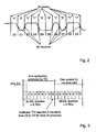
- Figure 2 shows a diagram of a symbol comprising 10 bits D0, D1, ... ,D9 and the respective logical values "1" or "0". In case that the logical value of a subsequent bit changes, a bit transition will be recognised in form of a falling or raising edge.
- the data processing unit 1, 2 follows some rules, which will be described in the following with respect to figure 2 .
- the transmitter of a data processing unit 1, 2 always performs dynamical adapting of a bit length, e.g. slow bit provision, in the data stream if required.
- the transmitter tries to use a slow bit whenever it is requested to do this and whenever it is allowed to provide a slow bit.
- bit transitions are candidate for slow bit provision.
- the transmitter is generally allowed to shorten (“fast bit”) or lengthen (“slow bit”) the bit length.
- Figure 3 shows a diagram of bits D3 and D4 wherein the bit length of bit D3 is adapted by inserting an additional TIC, i.e. one additional clock cycle of the local clock oscillator 6. This extension can take place since there is a transition from bit D3 to D4.
- the oversampling factor of 8 is used. This divides the symbol bit D3 into 9 slots, whereas symbol bit D4 is a period that can be divided in 8 slots.
- the master data processing unit 1 provides slow bits according to the contents of a slow bit register.
- the number of slow bits used for a specific configuration of the system is already known at system start and written to the slow bit register only once. Thus, if the slow bit register is set to 100, only one slow bit is inserted after 100 normal data bits which have been forwarded to the data bus 3. The slow bit provision will be delayed if there is no transition at the 100th bit position. Provision of the slow bit will take place on the falling or raising edge that must be transmitted to the system.
- the downstream transmission frequency can be generated in the master data processing unit 1 in two different ways.
- the phase-locked-loop PLL of the local clock oscillator 6 of the master data processing unit 1 is configured to exact the frequency that is required. No slow bits are sent from the master data processing unit 1 to the downstream channel in this case.
- the phase-locked-loop PLL of the master data processing unit 1 can be configured to a frequency close to the local clock oscillator signal f S of the local clock oscillators 6 of the slave data processing units 2.
- the master data processing unit 1 includes slow bits to reduce the effective data transmission frequency.
- the bit sampling point in the slave device will shift towards the bit border, if the bits were generated by a master frequency f M that is far away from the slave frequency f S . In contrast, if the slave frequency f S and the master frequency f M are close to each other, the sampling point will remain more reliable in the middle of the bit.
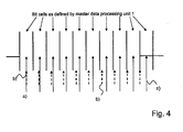
- Figure 4 shows a diagram of the sampling point shift.
- the distance between the vertical lines are the bit cells as defined by the master data processing unit 1.
- the arrows a) are showing the sampling event in the middle of the bit cell in case that the slave frequency f S is close to the master frequency f M .
- the arrows b) are showing the sampling shifts to the bit border due to a deviation between the slave frequency f S and the master frequency f M .
- the slave data processing units 2 inserts TIC's for lengthening bits according to the number of bits that are available in the transmission bit FIFO-register and according to the programmed transmitter FIFO-threshold.
- a slow bit request is signalled to the processor 5 or to the interface 4 of the slave data processing unit 2 whenever the number of bits available in the transmission FIFO-register is lower than the programmed FIFO-threshold. If this is the case, the transmitter starts to adapt the bit length of a sequence of bits as much as possible.
- the slow bit request is negated to void transmission FIFO-register overflow.
- the comparison of the number of bits in the FIFO-register to the threshold introduces a simple control loop.
- This control loop outputs only two states. One state is to request slow bits to be provided, the other state is to transmit only normal bits.
- the processor 5 or transmitter in the interface 4 of a slave data processing unit 2 takes care of the rule that slow bits are allowed only when the transmitted logic level changes.
- a logic level change might be a positive or a negative transition. If the transmitter outputs a steady state value, the slow bit request is temporarily registered in a counter. The transmission of one or more slow bits is delayed in this case.
- the rule that the slave oversampling clock frequency f S is always greater than the master oversampling clock frequency f M can be secured by design of the local clock oscillator 6.
- the rule that the maximum slave oversampling clock frequency f Smax is always below or equal to the maximum oversampling clock frequency f max of all data processing units 1, 2 of the system can also be fulfilled by the design if components in configuration are chosen in an appropriate way.
- the maximum slow bit provision is one TIC per bit
- a restriction adaption is provided.
- the duration of one bit within a symbol can be 8 TIC's or 9 TIC's. No other values are possible.
- the maximum duration of such a sequence is (8 x N) or ((8 x N) + 1) TIC's, where N is a number of consecutive bits having identical value.
- the rule of the 8b /10b-coding scheme allows to consider at least three transitions per symbol. For this scheme, no symbols with less than three transitions exist. This number does not include a possible transition at the border of symbols.
- the amount of data that is transferred by the master to its output must be same amount of data that enters the first slave device at its receiver input.
- a number of "N" bits of data generated by the master with its transmission clock f M must also be generated by the slave at its output, but with the slave frequency f S . Since the slave operates at a higher frequency, it must add slow bits into its output data stream. If no slow bits were added, the FIFO of the slave device would enter an underrun condition. Each slow bit that is added to the outgoing data stream has duration of 1/f S . For a longer data stream, "K" slow bits must be added to the data stream to avoid FIFO underrun. This relationship can be written down in a formula that describes the time for transmission of the bit stream. The time must be the same for master and slave.
- the left side is the time required by the master to transmit a bit stream with the length of "N" bits.
- the right side includes the time required by the slave device for data bit transmission plus a number of slow bits.
- K the number of slow bits is achieved that must be transmitted for a data stream with a length of "N” bits.
- the slave clock frequency cannot be higher than 1.25 the master clock frequency if one slow bit can be inserted for one standard bit.
Landscapes
- Engineering & Computer Science (AREA)
- Computer Networks & Wireless Communication (AREA)
- Signal Processing (AREA)
- Synchronisation In Digital Transmission Systems (AREA)
- Communication Control (AREA)
Abstract
Description
- The invention relates to a method for synchronising communication of a plurality of data processing units over a data bus, each of the data processing units comprising local clock oscillators providing clock signals for synchronising digital data communication, wherein a first data processing unit is provided as a master data processing unit synchronising the timing of data communication and controlling data communication of controlled slave data processing units.
- The invention further relates to data processing units comprising an interface provided for data communication of a data bus, a local clock oscillator providing a local clock oscillator signal and a processor unit provided for data processing and control of communication of data bit streams comprising a sequence of bits over the data bus.
- Data communication of a data bus is wide spread used in the computer technique. Especially for control systems comprising a master controller and a plurality of input/output-units, connected to the master controller by an internal system bus, synchronising of the data communication is required. The master controller additionally provides a data communication system with other devices connected to the master controller by a field bus. Often, the internal system bus is designed in ring bus topology so, that a bit data stream is sequentially forwarded from the master controller through a sequence of input/output-units.
- In order to synchronise the data communication, the master controller sends data frames comprising a defined number of symbols, each symbol having a fixed number of bits periodically so, that the time length of a data frame is constant. In case that the data processing units are provided with local clock oscillators, no common time base is available. It is therefore a problem to achieve a constant time length of the data frames received or sent by a data processing unit. Thus, a data frame sent by a slave data processing unit might be shorter or longer as the standard data frame of a time length defined by the local clock oscillator of the master data processing unit. Further, the sampling of a data frame via a slave data processing unit might cause errors, when the clock cycle of the slave data processing unit differs from the standard clock cycle of the master data processing unit setting the time length of the sampled data frame.
- In order to compensate time differences between the master clock cycles and the slave clock cycles it is known to add or to remove symbols or to add or remove bit of symbols. The problem is that when adding or removing symbols, an error in the data message occurs. Further, an exact number of bits per symbol is often required for certain data communication. It is further known to dynamically adjust the local oscillator of slave data processing units to the master clock cycle defined by the master local clock oscillator of the master data processing unit. This requires exact time signals to be communicated via the data bus. Many data communication systems do not allow transmission and use of such critical timing signals.
- Object of the present invention is to provide an improved method for synchronising communication of a plurality of data processing units, especially for use in asynchronous communication systems.
- The object is achieved by the aforementioned method in, that at least one bit length of a sequence of bits to be communicated over the data bus is dynamically adapted to adjust a clock cycle difference between a master clock cycle based upon the local clock oscillator signal of the master data processing unit and a slave clock cycle based upon the local clock oscillator signal of a slave data processing unit.
- According to the present invention, the time length of a data frame, i.e. a sequence of data bits, e.g. a sequence of symbols comprising a defined number of bits, is varied simply by shorten or lengthen the time length of at least one.bit compared to a standard bit length defined by a clock cycle depending on the local clock oscillator signal.
- In contrast to a synchronising communication by adding or removing bits of a bit data stream, the information content remains unchanged in the method according to the present invention. Further, no control of the local clock oscillators is required.
- Preferably, at least one slow bit is provided into the data bit stream, said slow bit having a longer time duration than the other bits of the bit sequence in order to adjust a faster slave clock cycle to a slower master clock cycle, which is slower than the slave clock cycle.
- Thus, in case that the local clock oscillator of the slave runs faster than the local clock oscillator of the master, the timing of the slave is delayed by extending the cycle time of at least one specific selected bit so, that the time length of the bit sequence including the slow bit corresponds to the time length of a corresponding sequence of the master data processing unit.
- Preferably, the slave clock cycles are set faster than the master clock cycle. This makes it easier to synchronise the communication, since only slow bits are to be inserted by prolongating the time duration of selected bits in the slave data processing units. A slave clock cycle being faster than the master clock cycle guarantees that the minimal clock cycle of the slave is always grater or equal than the maximal clock cycle of the master.
- In a preferred embodiment, one / eight of the bit length of a standard bit length of a bit sequence is added to at least one selected bit in order to adapt the bit length of the sequence of bits. The standard bit length is defined by the slave clock cycle based upon the slave local clock oscillator system signal.
- In a preferred embodiment, the bit length of a sequence of bits is adapted by amending the bit length of a bit only after transition in the bit sequence. A transition in the sequence can be a rising or falling edge in the bit signal. Thus, a constant bit value bit sequence acts as a single bit. Only one duration of one oversampling clock cycle, i.e. extension or shortening of a bit length can be added to this kind of bit sequence in order to avoid unwanted communication errors.
- The dynamical adaption of the bit length can be controlled in dependence of a data overflow in the process of data communication. For example, a FIFO-register (shift register) in a data processing unit provided for receiving or transmitting of a bit data stream over the data bus controls the dynamical adaption. In case of an estimated or occurring data overflow or underflow in the FIFO-register the bit length of at least one bit of the bit sequence is extended or shortened to match the timing of the slave data processing unit and the master data processing unit.
- Further, the master clock cycle of a first master data processing unit can be variably adapted by adjusting the time between a sequence of time flags provided in a bit data stream through adapting the bit length of the bit data stream in order to synchronise the first master clock cycle with a second master clock cycle of a second master communicating with the first master data processing. Thus, the method according to the present invention can also be used for synchronising communication between two systems each controlled by a master data processing unit
- In a preferred embodiment, the digital bit data stream is coded by use of an 8 b/10b-code. In the 8b/10b-code a symbol comprising 8 bits is transmitted by use of symbols containing 10 bits. In the 8 b /10 b scheme, at least three transitions per symbol exist. In case that a bit having an adapted bit length is provided only after transition in the symbol, at least three adaptions may take place.
- A further object of the present invention is to provide an improved data processing unit comprising an interface provided for data communication over data bus, a local clock oscillator providing a local clock oscillator signal and a processor unit provided for data processing and control of communication of data bit streams comprising a sequence of bits over the data bus.
- The object is achieved by the data processing unit in that the processor unit is provided for dynamically adapting the bit length of a sequence of bits to be communicated over the data bus to adjust a clock cycle difference between a master clock cycle based upon the local clock oscillator signal of the master data processing unit and a slave clock cycle based upon the local clock oscillator signal of a slave data processing unit.
- The data processing unit is provided for performing the aforementioned method.
- The invention is further explained in detail by way of example with the enclosed drawings, in which
- Figure 1 -
- shows a block diagram of a system comprising master and slave data processing units communicating with each other over a data bus;
- Figure 2 -
- shows a time diagram of bit borders and bit transitions of a symbol comprising 10 bits;
- Figure 3 -
- shows two following bits, wherein the time length of the first bit is extended;
- Figure 4 -
- shows a diagram of sampling points and a shift of sampling points when the master and slave clock cycles differ from each other.
-
Figure 1 shows a block diagram of an asynchronous communication system comprising a masterdata processing unit 1 and a plurality of slavedata processing units data processing units data bus 3. Thedata bus 3 runs as an internal system bus. - The slave
data processing units 2 can be input/output-modules of a field bus control system, wherein the masterdata processing device 1 is a field bus modul coupling the system to a field bus. The system supports data transfers from the masterdata processing unit 1 to the slavedata processing units 2 and vice versa. The data transfer channel from the masterdata processing unit 1 to the slavedata processing unit 2 is named downstream channel. The data transfer channel from the slavedata processing unit 2 to the masterdata processing unit 1 is named upstream channel. Both channels use the same communication structure for transmission and for reception of data. Depending on the system application, data transfers may take place at the same time on both channels, thus allowing full duplex data transfer. - Each of the master and slave
data processing units interface 4 for controlling data communication over thedata bus 3. Further, thedata processing units processor 5 for data processing and control of communication of data bit streams. Thedata processor 5 or theinterface 4 comprises a FIFO-register for buffering a bit data stream, which is forwarded through thedata processing units - The
processors 5 of thedata processing units local clock oscillators 6, wherein eachdata processing unit local clock oscillator 6. Thelocal clock oscillators 6 provides a clock signal in order to set a clock cycle to control the bit length or symbol length respectively. - The master
data processing unit 1 and the slavedata processing unit 2 provides two transmitter paths and two receiver paths. Using these paths, the master and the slave devices are connected in serious. For the downstream data channel, a receiver path of an I/O module always connects to the transmitter path of its physical predecessor. The first transmitter in the system is the masterdata processing unit 1. For the upstream data channel, the transmitter path of a slave data processing unit 2 (I/O-module) always connects to the receiver path of its physical predecessor. The last receiver on the upstream data path is the master data processing unit. - Due to this connection scheme, the system behaves like a closed loop that has a specific amount of data flowing in it. Any amount of data that enters into any of the
data processing units data processing unit 2 on a transmission path. This applies to the downstream channel and to the upstream channel as well. This behaviour is independent of the baudrate and independent of the masterdata processing unit 1 or the clock frequency of the slavedata processing unit 2. - The master
data processing unit 1 always determines the baudrate of the system. The slavedata processing unit 2 can only follow the master baudrate. They never can change the baudrate of a system that has been configured once after the initial power-on-cycle has been finished. The final mean baudrate that is used in the system is determined after baudrate selection and baudrate tuning have been performed. - In order to tune the baudrate for synchronising the communication between the
data processing units data bus 3 is dynamically adapted by control of theprocessor 5 of adata processing unit data processing units local clock oscillators 6 of the plurality ofdata processing units - Data transmission takes place in symbols. One symbol transmitted via the
data bus 3 corresponds to one byte of data. However, a 8 b /10 b-coding scheme is used for data communication, so that one byte of data that is fed into a transmitter of adata processing unit data processing unit - Each of the transmitters and receivers operate on an oversampling clock controlled by the
local clock oscillator 6. The oversampling clock is a fixed multiple of the baudrate of the system. Due to oversampling, each symbol bit is divided into small portions, having the duration of the reciprocal of the oversampling clock. The small portion of a symbol bit is called a TIC. - The relation between the oversampling clock and the symbol duration is described by the oversampling factor. The oversampling factor might be always set to 8.
- Since one symbol contains 10 bits and each of these bits is divided into 8 TIC's, the nominal duration of one symbol is 80 TIC's.
- Each of the master and slave
data processing units local clock oscillators 6. However, it is assumed that the oversampling frequency of thedata processing units data processing units data processing unit data processing unit data processing unit - Since there is no physical line available that allows transmitting a synchronisation clock signal between all
data processing units - In the method, the local master
data processing unit 1 should be operated on an oversampling frequency that is in a well-known range below the oversampling frequencies of the slave data processing units. Each of the slavedata processing unit 2 has an oversampling frequency that is in a well-known range above the master oversampling frequency. Since all the slavedata processing units 2 run faster than the masterdata processing unit 1 does, the slavedata processing units 2 are provided to reduce their baudrate to keep track with the baudrate that is used by the masterdata processing unit 1. - For baudrate reduction, the slave
data processing unit 2 provides slow bits as required when transmitting symbols. That is, the bit length of selected bits of a symbol is increased, e.g. by use of a reduced number of TIC's. One TIC is the duration of one oversampling clock cycle, so that one bit is transmitted by use of a plurality of clock cycles. - Even the master
data processing unit 1 might use slow bits to reduce its own baudrate to a value that is known to be lower than the baudrate of the slowest slavedata processing unit 2. The number of slow bits having an increased bit length is decided by an internal control loop of the slavedata processing units 2. In the masterdata processing unit 1, slow bits should be provided in fixed programmed intervals. A slow bit is a period extension of a symbol bit by one TIC or a plurality (two, three, four, ...) of TICs. The period extension should always be one TIC or a plurality of TIC's. In case that the duration of a bit comprises the sequence of 8 TIC's, a symbol bit that is extended by a slow bit has a period of 9 TIC's. The logic level of the symbol bit does not change during the additional TIC. -
Figure 2 shows a diagram of a symbol comprising 10 bits D0, D1, ... ,D9 and the respective logical values "1" or "0". In case that the logical value of a subsequent bit changes, a bit transition will be recognised in form of a falling or raising edge. - In case that the duration of a bit must be adapted, the
data processing unit figure 2 . - The transmitter of a
data processing unit - As a rule, the bit transitions are candidate for slow bit provision. In case that the transition in form of a raising or falling edge is recognised, the transmitter is generally allowed to shorten ("fast bit") or lengthen ("slow bit") the bit length.
-
Figure 3 shows a diagram of bits D3 and D4 wherein the bit length of bit D3 is adapted by inserting an additional TIC, i.e. one additional clock cycle of thelocal clock oscillator 6. This extension can take place since there is a transition from bit D3 to D4. In the example shown infigure 3 , the oversampling factor of 8 is used. This divides the symbol bit D3 into 9 slots, whereas symbol bit D4 is a period that can be divided in 8 slots. - The master
data processing unit 1 provides slow bits according to the contents of a slow bit register. The number of slow bits used for a specific configuration of the system is already known at system start and written to the slow bit register only once. Thus, if the slow bit register is set to 100, only one slow bit is inserted after 100 normal data bits which have been forwarded to thedata bus 3. The slow bit provision will be delayed if there is no transition at the 100th bit position. Provision of the slow bit will take place on the falling or raising edge that must be transmitted to the system. - The downstream transmission frequency can be generated in the master
data processing unit 1 in two different ways. The phase-locked-loop PLL of thelocal clock oscillator 6 of the masterdata processing unit 1 is configured to exact the frequency that is required. No slow bits are sent from the masterdata processing unit 1 to the downstream channel in this case. On the other hand, the phase-locked-loop PLL of the masterdata processing unit 1 can be configured to a frequency close to the local clock oscillator signal fS of thelocal clock oscillators 6 of the slavedata processing units 2. The masterdata processing unit 1 includes slow bits to reduce the effective data transmission frequency. - In the second solution, the bit sampling point in the slave device will shift towards the bit border, if the bits were generated by a master frequency fM that is far away from the slave frequency fS. In contrast, if the slave frequency fS and the master frequency fM are close to each other, the sampling point will remain more reliable in the middle of the bit.
- Since slow bits are only inserted at the border of bits, they do not have impact on the sampling point. This is especially true for the comma characters that have a number of 5 bits set to the same value.
-
Figure 4 shows a diagram of the sampling point shift. The distance between the vertical lines are the bit cells as defined by the masterdata processing unit 1. The arrows a) are showing the sampling event in the middle of the bit cell in case that the slave frequency fS is close to the master frequency fM. - The arrows b) are showing the sampling shifts to the bit border due to a deviation between the slave frequency fS and the master frequency fM.
- The use of slow bits (or fast bits) having a variable bit length by the master
data processing unit 1 is therefore recommended in order to improve the robustness of the data transmission. - The rule for adapting the bit length of a sequence of bits by the slave
data processing units 2 are explained in the following. - The slave
data processing units 2 inserts TIC's for lengthening bits according to the number of bits that are available in the transmission bit FIFO-register and according to the programmed transmitter FIFO-threshold. A slow bit request is signalled to theprocessor 5 or to theinterface 4 of the slavedata processing unit 2 whenever the number of bits available in the transmission FIFO-register is lower than the programmed FIFO-threshold. If this is the case, the transmitter starts to adapt the bit length of a sequence of bits as much as possible. When the FIFO-register is filled up to the programmed level, the slow bit request is negated to void transmission FIFO-register overflow. - The comparison of the number of bits in the FIFO-register to the threshold introduces a simple control loop. This control loop outputs only two states. One state is to request slow bits to be provided, the other state is to transmit only normal bits.
- However, the
processor 5 or transmitter in theinterface 4 of a slavedata processing unit 2 takes care of the rule that slow bits are allowed only when the transmitted logic level changes. A logic level change might be a positive or a negative transition. If the transmitter outputs a steady state value, the slow bit request is temporarily registered in a counter. The transmission of one or more slow bits is delayed in this case. - The process of dynamically adapting the bit length of the sequence of bits is based on three rules:
- a) the maximum slow bit provision is one TIC per bit;
- b) the additional TIC can only be inserted after a falling or rising bit edge;
- c) the symbol transmission in the system is based on 8b/10b encoding / decoding.
- Further, the ranges of the oversampling clock frequencies are defined as follows:
- a)

- b)

- c)

- The rule that the slave oversampling clock frequency fS is always greater than the master oversampling clock frequency fM can be secured by design of the
local clock oscillator 6. - Further, the rule that the maximum slave oversampling clock frequency fSmax is always below or equal to the maximum oversampling clock frequency fmax of all
data processing units - The rule that the maximum difference of the maximum slave oversampling clock frequency fSmax and the minimal master oversampling clock frequency fMmin is always below or equal the threshold Δmax requires the aforementioned rules.
- From the rule that the maximum slow bit provision is one TIC per bit, a restriction adaption is provided. For x8 oversampling, the duration of one bit within a symbol can be 8 TIC's or 9 TIC's. No other values are possible.
- From the rule that the additional TIC can only be inserted after a falling or rising bit edge, only one TIC can be added to this kind of bit sequence. Thus, the maximum duration of such a sequence is (8 x N) or ((8 x N) + 1) TIC's, where N is a number of consecutive bits having identical value.
- The rule of the 8b /10b-coding scheme allows to consider at least three transitions per symbol. For this scheme, no symbols with less than three transitions exist. This number does not include a possible transition at the border of symbols.
- The previous consideration will now be applied to a bit stream that is transmitted within the system.
- The bit stream consists of "N" bits. Each bit has duration of TBIT. The duration of each bit is also equal to the duration of 8 oversampling clocks or equal to 8 TIC's. The duration of one TIC is 1/fM since we assumed the master transmits the bit stream. The time required by the master to transmit the entire bit steam is

- The equation shown above does not include any slow bit. For each of the bits, exactly 8 TIC's are assumed.
- The amount of data that is transferred by the master to its output must be same amount of data that enters the first slave device at its receiver input. Now, a number of "N" bits of data generated by the master with its transmission clock fM must also be generated by the slave at its output, but with the slave frequency fS. Since the slave operates at a higher frequency, it must add slow bits into its output data stream. If no slow bits were added, the FIFO of the slave device would enter an underrun condition. Each slow bit that is added to the outgoing data stream has duration of 1/fS. For a longer data stream, "K" slow bits must be added to the data stream to avoid FIFO underrun. This relationship can be written down in a formula that describes the time for transmission of the bit stream. The time must be the same for master and slave. The equation is

- In this equation, the left side is the time required by the master to transmit a bit stream with the length of "N" bits. The right side includes the time required by the slave device for data bit transmission plus a number of slow bits. Solving this equation for "K", the number of slow bits is achieved that must be transmitted for a data stream with a length of "N" bits.

- Changing the equation points out the number of slow bits that are required for transmission of one standard data bit (not stretched).

- The equation shown above points out that the number of slow bits that must be transmitted for one data bit depends on the ratio of the clock frequencies that are used in the master and slave devices. The ratio fS/fM is > 1 if the three fundamental rules have been observed. Thus, K will always be a positive number.
- However, there are more limitations that must be taken into account. As an example, one might use a slave clock frequency of 512 MHz and a master clock frequency of 1 MHz. Using these values, the ratio K/N will be 511. This implies the transmission of 511 slow bits for each standard bit. This case is not allowed since the system cannot transmit more than one slow bit per standard bit. With a maximum of one slow bit per standard bit, the above equation is rewritten to reflect this case. Substituting K/N by 1, the result is

- Modifying the equation shown above points out the real limits on the frequency ratio.

- The slave clock frequency cannot be higher than 1.25 the master clock frequency if one slow bit can be inserted for one standard bit.
- Things change when the other rules are taken into account. In the 8b/10b scheme three transitions per symbol exist. Each symbol contains 10 bits. A slow bit can be introduced only after a bit transition in the symbol. Therefore, the
equation 1 ≥ 8 * (fS / fM -1) is rewritten to include this rule.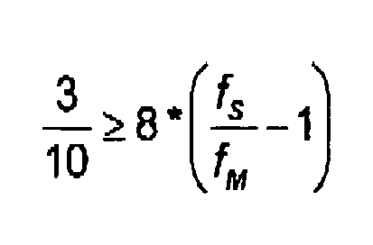
- This relationship is worse than the previous one since now only three of ten symbols can be extended to be a slow bit. Rewriting of the equation points out the maximum acceptable frequency ratio between the master and the slave clock frequency for the 8b/10 scheme.

- This equation is now ready to be applied to one of the fundamental equations, stating that the slave frequency must always be higher than the master frequency. Using these values, the analytical result for Δ max is obtained.

- The equation shown above states that the minimum master frequency multiplied by 103,75% must be larger than the maximum slave frequency. It should be notet, that 1.0375*fMmin is only a theoretical value that will never appear within the system. Δmax for the 8b/10b scheme is 3.75%.
Claims (12)
- Method for synchronising communication of a plurality of data processing units (1, 2) over data bus (3), each of the data processing units (1, 2) comprising local clock oscillators (6) providing clock signals for synchronising digital data communication, wherein a first data processing unit is provided as a master data processing unit (1), synchronising the timing for data communication and controlling the data communication of controlled slave data processing units (2), characterised by dynamically adapting the bit length of a sequence of bits to be communicated over the data bus (3) to adjust a clock cycle difference between a master clock cycle based upon the local clock oscillator signal of the master data processing unit (1) and a slave clock cycle based upon the local clock oscillator signal of a slave data processing unit (2).
- Method according to claim 1, characterised by providing at least one slow bit having a longer time duration than the other bits of a bit sequence in order to adjust a faster slave clock cycle to a slower master clock cycle, which is slower than the slave clock cycle.
- Method according to claim 2, characterised by setting the slave clock cycles faster than the master clock cycle.
- Method according to claim 2 or 3, characterised by adding 1/8 of the bit length of a standard bit length of a bit sequence, the standard bit length being defined by the slave clock cycle based upon the slave local clock oscillator signal.
- Method according to one of preceding claims, characterised by adapting the bit length of a sequence of bits by amending the bit length of a bit only after transition in the bit sequence.
- Method according to claim 5, characterised in that a transition is assumed when recognising a rising edge in the bit signal.
- Method according to claim 5, characterised in that a transition is assumed when recognising a falling edge in the bit signal.
- Method according to one of the preceding claims, characterised by controlling dynamically adaption of the bit length in dependence on a data overflow in the process of data communication.
- Method according to one of the preceding claims, characterised by variably adapting a first master clock cycle of a first master data processing unit (1) by adjusting the time between a sequence of time flags provided in a digital bit data stream through adapting the bit length of bits in the bit data stream in order to synchronise the first master clock cycle with a second master clock cycle of a second master data processing unit communicating with the first master data processing unit (1).
- Method according to one of the preceding claims, characterised by use of a 8 b /10 b-code, wherein 8 bit symbols of the data bit stream are a coded by symbols having a length of 10 bit.
- Data processing unit (1, 2) comprising an interface (4) provided for data communication over a data bus (3), a local clock oscillator (6) providing a local clock oscillator signal and a processing unit (5) provided for data processing and control of communication of data bit streams comprising a sequence of bits over the data bus (3), characterised in, that the processing unit is provided for dynamically adapting the bit length of a sequence of bits to be communicated over the data bus (3) to adjust a clock cycle difference between a master clock cycle based upon the local clock oscillator signal of a master data processing unit (1) and the clock cycle of the data processing unit (1,2) based upon the local clock oscillator signal of the data processing unit (1, 2).
- Data processing unit (1, 2) according to claim 11, characterised in that the data processing unit (1, 2) is provided for performing the method according to claims 1 to 10.
Priority Applications (3)
| Application Number | Priority Date | Filing Date | Title |
|---|---|---|---|
| AT06025570T ATE463896T1 (en) | 2006-12-11 | 2006-12-11 | DATA PROCESSING UNIT AND METHOD FOR SYNCHRONIZING COMMUNICATION BETWEEN DATA PROCESSING UNITS |
| EP06025570A EP1933494B1 (en) | 2006-12-11 | 2006-12-11 | Data processing unit and method for synchronising communication of a plurality of data processing units |
| DE602006013489T DE602006013489D1 (en) | 2006-12-11 | 2006-12-11 | Data processing unit and method for synchronizing communication between data processing units |
Applications Claiming Priority (1)
| Application Number | Priority Date | Filing Date | Title |
|---|---|---|---|
| EP06025570A EP1933494B1 (en) | 2006-12-11 | 2006-12-11 | Data processing unit and method for synchronising communication of a plurality of data processing units |
Publications (2)
| Publication Number | Publication Date |
|---|---|
| EP1933494A1 true EP1933494A1 (en) | 2008-06-18 |
| EP1933494B1 EP1933494B1 (en) | 2010-04-07 |
Family
ID=37907075
Family Applications (1)
| Application Number | Title | Priority Date | Filing Date |
|---|---|---|---|
| EP06025570A Not-in-force EP1933494B1 (en) | 2006-12-11 | 2006-12-11 | Data processing unit and method for synchronising communication of a plurality of data processing units |
Country Status (3)
| Country | Link |
|---|---|
| EP (1) | EP1933494B1 (en) |
| AT (1) | ATE463896T1 (en) |
| DE (1) | DE602006013489D1 (en) |
Cited By (3)
| Publication number | Priority date | Publication date | Assignee | Title |
|---|---|---|---|---|
| EP2187560A1 (en) * | 2008-11-14 | 2010-05-19 | Phoenix Contact GmbH & Co. KG | Field bus system with spread spectrum |
| US9021292B2 (en) | 2011-05-20 | 2015-04-28 | Texas Instruments Incorporated | Method and system for asynchronous serial communication in a ring network by generating an oversampling clock using a fractional rate multiplier and sampling a received data bit sequence that includes voltage and temperature information in a battery management system |
| WO2018215286A1 (en) * | 2017-05-24 | 2018-11-29 | Wago Verwaltungsgesellschaft Mbh | Distributed processing of process data |
Citations (4)
| Publication number | Priority date | Publication date | Assignee | Title |
|---|---|---|---|---|
| US4210777A (en) | 1978-06-15 | 1980-07-01 | Frederick Electronics Corp. | Pseudo-transparent stop bit generator |
| GB2072463A (en) | 1980-03-11 | 1981-09-30 | Vanderhoff Communications Ltd | Speech and data communication network |
| WO1999046861A1 (en) * | 1998-03-11 | 1999-09-16 | Thomson Licensing S.A. | Digital signal modulation system |
| EP1209814A1 (en) * | 2000-11-17 | 2002-05-29 | Eric Lukac-Kuruc | Process to expand data density |
-
2006
- 2006-12-11 EP EP06025570A patent/EP1933494B1/en not_active Not-in-force
- 2006-12-11 AT AT06025570T patent/ATE463896T1/en not_active IP Right Cessation
- 2006-12-11 DE DE602006013489T patent/DE602006013489D1/en active Active
Patent Citations (4)
| Publication number | Priority date | Publication date | Assignee | Title |
|---|---|---|---|---|
| US4210777A (en) | 1978-06-15 | 1980-07-01 | Frederick Electronics Corp. | Pseudo-transparent stop bit generator |
| GB2072463A (en) | 1980-03-11 | 1981-09-30 | Vanderhoff Communications Ltd | Speech and data communication network |
| WO1999046861A1 (en) * | 1998-03-11 | 1999-09-16 | Thomson Licensing S.A. | Digital signal modulation system |
| EP1209814A1 (en) * | 2000-11-17 | 2002-05-29 | Eric Lukac-Kuruc | Process to expand data density |
Cited By (5)
| Publication number | Priority date | Publication date | Assignee | Title |
|---|---|---|---|---|
| EP2187560A1 (en) * | 2008-11-14 | 2010-05-19 | Phoenix Contact GmbH & Co. KG | Field bus system with spread spectrum |
| US8406269B2 (en) | 2008-11-14 | 2013-03-26 | Phoenix Contact Gmbh & Co. Kg | Field bus system using spread spectrum |
| US9021292B2 (en) | 2011-05-20 | 2015-04-28 | Texas Instruments Incorporated | Method and system for asynchronous serial communication in a ring network by generating an oversampling clock using a fractional rate multiplier and sampling a received data bit sequence that includes voltage and temperature information in a battery management system |
| WO2018215286A1 (en) * | 2017-05-24 | 2018-11-29 | Wago Verwaltungsgesellschaft Mbh | Distributed processing of process data |
| US11184194B2 (en) | 2017-05-24 | 2021-11-23 | Wago Verwaltungsgesellschaft Mbh | Distributed processing of process data |
Also Published As
| Publication number | Publication date |
|---|---|
| DE602006013489D1 (en) | 2010-05-20 |
| EP1933494B1 (en) | 2010-04-07 |
| ATE463896T1 (en) | 2010-04-15 |
Similar Documents
| Publication | Publication Date | Title |
|---|---|---|
| US11804919B2 (en) | High speed embedded protocol for distributed control system | |
| US7328359B2 (en) | Technique to create link determinism | |
| EP3030972B1 (en) | N-phase signal transition alignment | |
| CN106464559B (en) | High-Speed Embedded Protocols for Distributed Control Systems | |
| US6687255B1 (en) | Data communication circuit having FIFO buffer with frame-in-FIFO generator | |
| US6128317A (en) | Transmitter and receiver supporting differing speed codecs over single links | |
| JP2004520778A (en) | Parallel data communication with skew-tolerant data groups | |
| US9047421B2 (en) | Serial link buffer fill-level compensation using multi-purpose start of protocol data unit timing characters | |
| US5131015A (en) | Combined BAUD rate generator and digital phase locked loop | |
| EP3267305B1 (en) | Circuit and method for credit-based flow control | |
| US6961691B1 (en) | Non-synchronized multiplex data transport across synchronous systems | |
| EP1933494B1 (en) | Data processing unit and method for synchronising communication of a plurality of data processing units | |
| US20060098770A1 (en) | Synchronizer for passing data from a first system to a second system | |
| US11411710B2 (en) | Subscriber of a data network | |
| CN119999116A (en) | Apparatus and method for processing transmit data in a transmit data path including parallel FEC encoding and data width conversion | |
| US7212598B2 (en) | Data buffer-controlled digital clock regenerator | |
| CN104063351B (en) | A kind of High-Speed Multiplexer synchronous serial interface method for designing for anti-collision of rattling | |
| EP1459186B1 (en) | Rate adaptation within a tdm switch using bit stuffing | |
| WO2004063836A2 (en) | Method and system for clock domain crossing and format adaptation using synchronous handshake protocol | |
| EP1573574B1 (en) | Synchronisation of semi-synchronous processing elements | |
| US12580789B1 (en) | Media access control (MAC) to physical coding sublayer (PCS) data rate synchronization circuitry | |
| EP1188108B1 (en) | Two clock domain pulse to pulse synchronizer | |
| US20250330199A1 (en) | Apparatus and method for processing receive data in a receive data path including parallel fec decoding | |
| US20030002589A1 (en) | Serial communication circuit and serial transmitting and receiving system | |
| KR101999125B1 (en) | Output signal automatic controller for RS-422 and RS-485 serial communication |
Legal Events
| Date | Code | Title | Description |
|---|---|---|---|
| PUAI | Public reference made under article 153(3) epc to a published international application that has entered the european phase |
Free format text: ORIGINAL CODE: 0009012 |
|
| AK | Designated contracting states |
Kind code of ref document: A1 Designated state(s): AT BE BG CH CY CZ DE DK EE ES FI FR GB GR HU IE IS IT LI LT LU LV MC NL PL PT RO SE SI SK TR |
|
| AX | Request for extension of the european patent |
Extension state: AL BA HR MK RS |
|
| AKX | Designation fees paid | ||
| 17P | Request for examination filed |
Effective date: 20090219 |
|
| RBV | Designated contracting states (corrected) |
Designated state(s): AT BE BG CH CY CZ DE DK EE ES FI FR GB GR HU IE IS IT LI LT LU LV MC NL PL PT RO SE SI SK TR |
|
| 17Q | First examination report despatched |
Effective date: 20090327 |
|
| GRAP | Despatch of communication of intention to grant a patent |
Free format text: ORIGINAL CODE: EPIDOSNIGR1 |
|
| RAP1 | Party data changed (applicant data changed or rights of an application transferred) |
Owner name: ACCENT S.P.A. |
|
| RAP1 | Party data changed (applicant data changed or rights of an application transferred) |
Owner name: WAGO KONTAKTTECHNIK GMBH (NACH SCHWEIZER RECHT) & |
|
| GRAS | Grant fee paid |
Free format text: ORIGINAL CODE: EPIDOSNIGR3 |
|
| GRAA | (expected) grant |
Free format text: ORIGINAL CODE: 0009210 |
|
| AK | Designated contracting states |
Kind code of ref document: B1 Designated state(s): AT BE BG CH CY CZ DE DK EE ES FI FR GB GR HU IE IS IT LI LT LU LV MC NL PL PT RO SE SI SK TR |
|
| REG | Reference to a national code |
Ref country code: GB Ref legal event code: FG4D |
|
| REG | Reference to a national code |
Ref country code: CH Ref legal event code: EP |
|
| REG | Reference to a national code |
Ref country code: IE Ref legal event code: FG4D |
|
| REF | Corresponds to: |
Ref document number: 602006013489 Country of ref document: DE Date of ref document: 20100520 Kind code of ref document: P |
|
| REG | Reference to a national code |
Ref country code: DE Ref legal event code: R096 Ref document number: 602006013489 Country of ref document: DE Effective date: 20100520 |
|
| REG | Reference to a national code |
Ref country code: NL Ref legal event code: VDEP Effective date: 20100407 |
|
| PG25 | Lapsed in a contracting state [announced via postgrant information from national office to epo] |
Ref country code: SI Free format text: LAPSE BECAUSE OF FAILURE TO SUBMIT A TRANSLATION OF THE DESCRIPTION OR TO PAY THE FEE WITHIN THE PRESCRIBED TIME-LIMIT Effective date: 20100407 |
|
| LTIE | Lt: invalidation of european patent or patent extension |
Effective date: 20100407 |
|
| PG25 | Lapsed in a contracting state [announced via postgrant information from national office to epo] |
Ref country code: ES Free format text: LAPSE BECAUSE OF FAILURE TO SUBMIT A TRANSLATION OF THE DESCRIPTION OR TO PAY THE FEE WITHIN THE PRESCRIBED TIME-LIMIT Effective date: 20100718 Ref country code: LT Free format text: LAPSE BECAUSE OF FAILURE TO SUBMIT A TRANSLATION OF THE DESCRIPTION OR TO PAY THE FEE WITHIN THE PRESCRIBED TIME-LIMIT Effective date: 20100407 Ref country code: NL Free format text: LAPSE BECAUSE OF FAILURE TO SUBMIT A TRANSLATION OF THE DESCRIPTION OR TO PAY THE FEE WITHIN THE PRESCRIBED TIME-LIMIT Effective date: 20100407 Ref country code: SE Free format text: LAPSE BECAUSE OF FAILURE TO SUBMIT A TRANSLATION OF THE DESCRIPTION OR TO PAY THE FEE WITHIN THE PRESCRIBED TIME-LIMIT Effective date: 20100407 |
|
| PG25 | Lapsed in a contracting state [announced via postgrant information from national office to epo] |
Ref country code: FI Free format text: LAPSE BECAUSE OF FAILURE TO SUBMIT A TRANSLATION OF THE DESCRIPTION OR TO PAY THE FEE WITHIN THE PRESCRIBED TIME-LIMIT Effective date: 20100407 Ref country code: LV Free format text: LAPSE BECAUSE OF FAILURE TO SUBMIT A TRANSLATION OF THE DESCRIPTION OR TO PAY THE FEE WITHIN THE PRESCRIBED TIME-LIMIT Effective date: 20100407 Ref country code: IS Free format text: LAPSE BECAUSE OF FAILURE TO SUBMIT A TRANSLATION OF THE DESCRIPTION OR TO PAY THE FEE WITHIN THE PRESCRIBED TIME-LIMIT Effective date: 20100807 Ref country code: AT Free format text: LAPSE BECAUSE OF FAILURE TO SUBMIT A TRANSLATION OF THE DESCRIPTION OR TO PAY THE FEE WITHIN THE PRESCRIBED TIME-LIMIT Effective date: 20100407 |
|
| PG25 | Lapsed in a contracting state [announced via postgrant information from national office to epo] |
Ref country code: CY Free format text: LAPSE BECAUSE OF FAILURE TO SUBMIT A TRANSLATION OF THE DESCRIPTION OR TO PAY THE FEE WITHIN THE PRESCRIBED TIME-LIMIT Effective date: 20100526 Ref country code: GR Free format text: LAPSE BECAUSE OF FAILURE TO SUBMIT A TRANSLATION OF THE DESCRIPTION OR TO PAY THE FEE WITHIN THE PRESCRIBED TIME-LIMIT Effective date: 20100708 Ref country code: PL Free format text: LAPSE BECAUSE OF FAILURE TO SUBMIT A TRANSLATION OF THE DESCRIPTION OR TO PAY THE FEE WITHIN THE PRESCRIBED TIME-LIMIT Effective date: 20100407 |
|
| PG25 | Lapsed in a contracting state [announced via postgrant information from national office to epo] |
Ref country code: PT Free format text: LAPSE BECAUSE OF FAILURE TO SUBMIT A TRANSLATION OF THE DESCRIPTION OR TO PAY THE FEE WITHIN THE PRESCRIBED TIME-LIMIT Effective date: 20100809 Ref country code: EE Free format text: LAPSE BECAUSE OF FAILURE TO SUBMIT A TRANSLATION OF THE DESCRIPTION OR TO PAY THE FEE WITHIN THE PRESCRIBED TIME-LIMIT Effective date: 20100407 Ref country code: DK Free format text: LAPSE BECAUSE OF FAILURE TO SUBMIT A TRANSLATION OF THE DESCRIPTION OR TO PAY THE FEE WITHIN THE PRESCRIBED TIME-LIMIT Effective date: 20100407 |
|
| PLBE | No opposition filed within time limit |
Free format text: ORIGINAL CODE: 0009261 |
|
| STAA | Information on the status of an ep patent application or granted ep patent |
Free format text: STATUS: NO OPPOSITION FILED WITHIN TIME LIMIT |
|
| PG25 | Lapsed in a contracting state [announced via postgrant information from national office to epo] |
Ref country code: CZ Free format text: LAPSE BECAUSE OF FAILURE TO SUBMIT A TRANSLATION OF THE DESCRIPTION OR TO PAY THE FEE WITHIN THE PRESCRIBED TIME-LIMIT Effective date: 20100407 Ref country code: RO Free format text: LAPSE BECAUSE OF FAILURE TO SUBMIT A TRANSLATION OF THE DESCRIPTION OR TO PAY THE FEE WITHIN THE PRESCRIBED TIME-LIMIT Effective date: 20100407 Ref country code: SK Free format text: LAPSE BECAUSE OF FAILURE TO SUBMIT A TRANSLATION OF THE DESCRIPTION OR TO PAY THE FEE WITHIN THE PRESCRIBED TIME-LIMIT Effective date: 20100407 Ref country code: BE Free format text: LAPSE BECAUSE OF FAILURE TO SUBMIT A TRANSLATION OF THE DESCRIPTION OR TO PAY THE FEE WITHIN THE PRESCRIBED TIME-LIMIT Effective date: 20100407 |
|
| 26N | No opposition filed |
Effective date: 20110110 |
|
| PG25 | Lapsed in a contracting state [announced via postgrant information from national office to epo] |
Ref country code: IT Free format text: LAPSE BECAUSE OF FAILURE TO SUBMIT A TRANSLATION OF THE DESCRIPTION OR TO PAY THE FEE WITHIN THE PRESCRIBED TIME-LIMIT Effective date: 20100407 |
|
| REG | Reference to a national code |
Ref country code: DE Ref legal event code: R097 Ref document number: 602006013489 Country of ref document: DE Effective date: 20110110 |
|
| PG25 | Lapsed in a contracting state [announced via postgrant information from national office to epo] |
Ref country code: MC Free format text: LAPSE BECAUSE OF NON-PAYMENT OF DUE FEES Effective date: 20101231 |
|
| REG | Reference to a national code |
Ref country code: CH Ref legal event code: PL |
|
| GBPC | Gb: european patent ceased through non-payment of renewal fee |
Effective date: 20101211 |
|
| REG | Reference to a national code |
Ref country code: FR Ref legal event code: ST Effective date: 20110831 |
|
| PG25 | Lapsed in a contracting state [announced via postgrant information from national office to epo] |
Ref country code: FR Free format text: LAPSE BECAUSE OF NON-PAYMENT OF DUE FEES Effective date: 20110103 Ref country code: LI Free format text: LAPSE BECAUSE OF NON-PAYMENT OF DUE FEES Effective date: 20101231 Ref country code: IE Free format text: LAPSE BECAUSE OF NON-PAYMENT OF DUE FEES Effective date: 20101211 Ref country code: CH Free format text: LAPSE BECAUSE OF NON-PAYMENT OF DUE FEES Effective date: 20101231 |
|
| PG25 | Lapsed in a contracting state [announced via postgrant information from national office to epo] |
Ref country code: GB Free format text: LAPSE BECAUSE OF NON-PAYMENT OF DUE FEES Effective date: 20101211 |
|
| PG25 | Lapsed in a contracting state [announced via postgrant information from national office to epo] |
Ref country code: BG Free format text: LAPSE BECAUSE OF FAILURE TO SUBMIT A TRANSLATION OF THE DESCRIPTION OR TO PAY THE FEE WITHIN THE PRESCRIBED TIME-LIMIT Effective date: 20100407 Ref country code: HU Free format text: LAPSE BECAUSE OF FAILURE TO SUBMIT A TRANSLATION OF THE DESCRIPTION OR TO PAY THE FEE WITHIN THE PRESCRIBED TIME-LIMIT Effective date: 20101008 Ref country code: LU Free format text: LAPSE BECAUSE OF NON-PAYMENT OF DUE FEES Effective date: 20101211 |
|
| PG25 | Lapsed in a contracting state [announced via postgrant information from national office to epo] |
Ref country code: TR Free format text: LAPSE BECAUSE OF FAILURE TO SUBMIT A TRANSLATION OF THE DESCRIPTION OR TO PAY THE FEE WITHIN THE PRESCRIBED TIME-LIMIT Effective date: 20100407 |
|
| PG25 | Lapsed in a contracting state [announced via postgrant information from national office to epo] |
Ref country code: BG Free format text: LAPSE BECAUSE OF FAILURE TO SUBMIT A TRANSLATION OF THE DESCRIPTION OR TO PAY THE FEE WITHIN THE PRESCRIBED TIME-LIMIT Effective date: 20100707 |
|
| REG | Reference to a national code |
Ref country code: DE Ref legal event code: R082 Ref document number: 602006013489 Country of ref document: DE Representative=s name: BARDEHLE PAGENBERG PARTNERSCHAFT PATENTANWAELT, DE Ref country code: DE Ref legal event code: R082 Ref document number: 602006013489 Country of ref document: DE Representative=s name: BARDEHLE PAGENBERG PARTNERSCHAFT MBB PATENTANW, DE |
|
| PGFP | Annual fee paid to national office [announced via postgrant information from national office to epo] |
Ref country code: DE Payment date: 20190228 Year of fee payment: 13 |
|
| PGFP | Annual fee paid to national office [announced via postgrant information from national office to epo] |
Ref country code: DE Payment date: 20190228 Year of fee payment: 13 |
|
| REG | Reference to a national code |
Ref country code: DE Ref legal event code: R119 Ref document number: 602006013489 Country of ref document: DE |
|
| PG25 | Lapsed in a contracting state [announced via postgrant information from national office to epo] |
Ref country code: DE Free format text: LAPSE BECAUSE OF NON-PAYMENT OF DUE FEES Effective date: 20200701 |
|
| P01 | Opt-out of the competence of the unified patent court (upc) registered |
Effective date: 20230516 |