EP1933334A1 - Method for producing superconducting wire and superconducting device - Google Patents
Method for producing superconducting wire and superconducting device Download PDFInfo
- Publication number
- EP1933334A1 EP1933334A1 EP06797051A EP06797051A EP1933334A1 EP 1933334 A1 EP1933334 A1 EP 1933334A1 EP 06797051 A EP06797051 A EP 06797051A EP 06797051 A EP06797051 A EP 06797051A EP 1933334 A1 EP1933334 A1 EP 1933334A1
- Authority
- EP
- European Patent Office
- Prior art keywords
- superconducting
- layer
- superconducting wire
- stabilization layer
- copper
- Prior art date
- Legal status (The legal status is an assumption and is not a legal conclusion. Google has not performed a legal analysis and makes no representation as to the accuracy of the status listed.)
- Granted
Links
Images

Classifications
-
- H—ELECTRICITY
- H10—SEMICONDUCTOR DEVICES; ELECTRIC SOLID-STATE DEVICES NOT OTHERWISE PROVIDED FOR
- H10N—ELECTRIC SOLID-STATE DEVICES NOT OTHERWISE PROVIDED FOR
- H10N60/00—Superconducting devices
- H10N60/01—Manufacture or treatment
- H10N60/0268—Manufacture or treatment of devices comprising copper oxide
- H10N60/0801—Manufacture or treatment of filaments or composite wires
-
- H—ELECTRICITY
- H01—ELECTRIC ELEMENTS
- H01B—CABLES; CONDUCTORS; INSULATORS; SELECTION OF MATERIALS FOR THEIR CONDUCTIVE, INSULATING OR DIELECTRIC PROPERTIES
- H01B12/00—Superconductive or hyperconductive conductors, cables, or transmission lines
- H01B12/02—Superconductive or hyperconductive conductors, cables, or transmission lines characterised by their form
- H01B12/06—Films or wires on bases or cores
Definitions
- the silver stabilization laver is formed to a thickness not more than 5 ⁇ m and the copper stabilization is formed to a thickness of at least 10 ⁇ m.
- a method of fabricating a superconducting wire that can reduce the manufacturing cost and increase the mechanical strength of the superconducting wire, and a superconducting apparatus including a superconducting wire obtained by the method can be provided.
- an intermediate layer 2 is formed on substrate 1.
- at least one electrically conductive layer selected from the group consisting of a cerium oxide layer, a yttria-stabilized-zirconia layer (YSZ laver), a GdZrO layer including gadolinia and zirxonia, and a magnesium oxide layer can be employed for intermediate layer 2.
- YSZ laver yttria-stabilized-zirconia layer
- GdZrO layer including gadolinia and zirxonia a magnesium oxide layer
- 1-x represents the composition ratio of ZrO 2 (zirconia), and x represents the composition ratio of Y 2 O 3 (yttria).
- x is a real number that satisfies 0.03 ⁇ x ⁇ 0.1.
- oxide superconductors of the Re-Ba-Cu-O system an oxide superconductor of the Ho-Ba-Cu-O system with a composition that is represented by a composition formula where Re in the composition formula (2) is replaced with Ho is preferably employed for superconducting layer 3.
- the thus obtained superconducting wire according to the present invention can be employed for superconducting apparatus such as superconducting cables, superconducting motors, generators, magnetic separation devices, magnets for single crystal growing furnaces, MRI (Magnetic Resonance Imaging), NMR (Nuclear Magnetic Resonance), linear motor cars or a transformer, for example.
- superconducting apparatus such as superconducting cables, superconducting motors, generators, magnetic separation devices, magnets for single crystal growing furnaces, MRI (Magnetic Resonance Imaging), NMR (Nuclear Magnetic Resonance), linear motor cars or a transformer, for example.
- a superconducting wire according to Comparative Example 3 was fabricated in the same method and conditions as in Example 1 except that the copper stabilization layer was not formed.
- a superconducting wire according to Example 3 was fabricated in the same method and conditions as in Example 1 except that the current density of the surface of the object to be plated was 2A/dm 2 in the electroplating and electroplating was performed for 23 minutes.
- Example 8 The appearance of the thus fabricated superconducting wire according to Example 8 was inspected in the same manner as in Example 1 and it was found that the superconducting wire according to Example 8 also had gloss and a smooth surface similarly to the superconducting wire according to Example 1 and that the copper stabilization layer had very high adhesion.
- a bending strain rate and a critical current were examined for the superconducting wires according to Examples 3 and 4 and Comparative Example 4. The results are shown in Fig. 7 .
- the horizontal axis shows a bending strain rate (%)
- the vertical axis shows a critical current value (relative value) at each bending strain rate with the critical current value when the bending strain rate is 0% defined as 1.
- a tensile stress and a critical current was examined for the superconducting wires according to Example 3 and 4 and Comparative Example 4, respectively.
- the results are shown in Fig. 8 .
- the horizontal axis shows a tensile stress (kg/mm 2 )
- the vertical axis shows a critical current value (relative value) at each tensile stress with the critical current value when the tensile stress is 0 defined as 1.
- the tensile stress in Fig. 8 is a tensile stress (kg) applied to the cross section of the superconducting wire per 1 mm 2 that is perpendicular to the tensile direction.
Landscapes
- Engineering & Computer Science (AREA)
- Manufacturing & Machinery (AREA)
- Superconductors And Manufacturing Methods Therefor (AREA)
- Inorganic Compounds Of Heavy Metals (AREA)
Abstract
Description
- The present invention relates to a method of fabricating a superconducting wire, and to a superconducting apparatus.
-
Fig. 9 schematically shows an example of a conventional superconducting wire in cross-section. The conventional superconducting wire has a structure in which anintermediate layer 2 composed of cerium oxide or yttria-stabilized-zirconia, for example, asuperconducting layer 3 composed of an oxide superconductor of a Ho-Ba-Cu-O system or a Y-Ba-Cu-O system, for example, and asilver stabilization layer 4 serving as a stabilization layer forsuperconducting layer 3 and composed of silver are successively laid on asubstrate 1 composed of a Ni alloy and the like (for example, seeFig. 1 of Japanese Patent Laying-Open No.07-37444 - In the above-mentioned conventional superconducting wire, variation in the amount of oxygen in the oxide superconductor forming
superconducting layer 3 significantly changes characteristics ofsuperconducting layer 3. Therefore, it is common to adjust the amount of oxygen in the oxide superconductor formingsuperconducting layer 3 by performing heat treatment aftersilver stabilization layer 4 is formed onsuperconducting layer 3. - There is a problem, however, that the fabrication cost is increased if a large amount of silver is used to form
silver stabilization layer 4 since silver is a relatively expensive material for an industrial material. In addition, there is also a problem that the superconducting wire cannot obtain enough mechanical strength ifsilver stabilization layer 4 is employed. - In order to solve such problems, there has been proposed a method to affix copper foil uniformly onto
superconducting layer 3 of a superconducting wire in a longitudinal direction by soldering. - Patent Document 1: Japanese Patent Laying-Open No.
07-37444 - In the aforementioned method to affix copper foil, however, there is a problem that a sophisticated technology is required to uniformly affix the copper foil onto the superconducting wire in the longitudinal direction by soldering and that poor adhesion between the copper foil and the superconducting layer is likely to cause peeling.
- In light of the aforementioned circumstances, an object of the present invention is to provide a method of fabricating a superconducting wire that can reduce the fabrication cost as well as can increase the mechanical strength of the superconducting wire, and a superconducting apparatus including a superconducting wire obtained by the method.
- The present invention provides a method of fabricating a superconducting wire including the steps of forming a superconducting layer on a substrate or an intermediate layer formed on the substrate, forming a silver stabilization layer on the superconducting layer, immersing the substrate in a copper sulfate solution after the superconducting layer and the silver stabilization layer are formed thereon, and forming a copper stabilization layer on the silver stabilization layer by electroplating with the copper sulfate solution as a plating bath. To note, in the present invention, another layer may be interposed between the substrate and the superconducting layer. In addition, another layer may be interposed between the superconducting layer and the silver stabilization layer.
- In the method of fabricating a superconducting wire according to the present invention, current density at the surface of an object to be plated is preferably less than 10A/dm2 in electroplating.
- In addition, in the method of fabricating a superconducting wire according to the invention, it is preferable that the silver stabilization laver is formed to a thickness not more than 5 µm and the copper stabilization is formed to a thickness of at least 10 µm.
- The present invention also provides a superconducting apparatus including a superconducting wire obtained by the above-described method of fabricating a superconducting wire.
- With the present invention, a method of fabricating a superconducting wire that can reduce the manufacturing cost and increase the mechanical strength of the superconducting wire, and a superconducting apparatus including a superconducting wire obtained by the method can be provided.
-
-
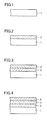
Fig. 1 is a schematic cross-sectional view of a preferred example of a substrate employed in the present invention. -
Fig. 2 is a schematic cross-sectional view of a preferred example of the substrate employed in the present invention after forming an intermediate layer. -
Fig. 3 is a schematic cross-sectional view of a preferred example of the substrate employed in the present invention after forming a superconducting layer. -
Fig. 4 is a schematic cross-sectional view of a preferred example of the substrate employed in the present invention after forming a silver stabilization layer. -
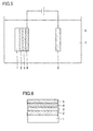
Fig. 5 is a schematic construction view of a preferred example of an electroplating device employed in the present invention. -
Fig. 6 is a schematic cross-sectional view of a preferred example of a superconducting wire according to the present invention. -
Fig. 7 shows the relation between a bending strain rate and a critical current in a superconducting wire according to the present invention and a conventional superconducting wire. -
Fig. 8 shows the relation between a tensile stress and a critical current in a superconducting wire according to the present invention and a conventional superconducting wire. -
Fig. 9 is a schematic cross-sectional view of an example of a conventional superconducting wire. - 1 substrate, 2 intermediate layer, 3 superconducting layer, 4 silver stabilization layer, 5 copper stabilization layer, 6 electrode, 7 copper sulfate solution, 8 container
- Hereinafter, a preferred example of a method of fabricating a superconducting wire according to the present invention will be described. To note, the same reference characters denote the same or corresponding elements in the drawings of the present invention.
- As shown in the schematic cross-sectional view of
Fig. 1 , asubstrate 1 in the form of a tape is prepared, for example. An electrically conductive substrate formed of an alloy including nickel as the main component can be employed forsubstrate 1, for example. It is preferable that an alloy including nickel as the main component is employed forsubstrate 1 and it is in particular preferable that the alloy including nickel as the main component includes tungsten. To note, "main component" in the present invention means to account for at least 50% of the total number of atoms that form the substrate. - Then, as shown in the schematic cross-sectional view of
Fig. 2 , anintermediate layer 2 is formed onsubstrate 1. For example, at least one electrically conductive layer selected from the group consisting of a cerium oxide layer, a yttria-stabilized-zirconia layer (YSZ laver), a GdZrO layer including gadolinia and zirxonia, and a magnesium oxide layer can be employed forintermediate layer 2. In particular, it is preferable that a three-layer structure in which a cerium oxide layer, a YSZ layer and a cerium oxide layer are successively laid onsubstrate 1 is used forintermediate layer 2. - Herein, the composition of the YSZ layer is represented by the Mowing composition formula (1):
(ZrO2)1-x(Y2O3)x (1)
- In the composition formula (1), 1-x represents the composition ratio of ZrO2 (zirconia), and x represents the composition ratio of Y2O3 (yttria). To note, in the composition formula (1), x is a real number that satisfies 0.03≤x≤0.1.
-
Intermediate layer 2 can be formed, for example, by at least one method selected from the group consisting of sputtering, laser abrasion, electron beam deposition, and IBAD (Ion Beam Assist Deposition). - Then, as shown in the schematic cross-sectional view of
Fig. 3 , asuperconducting layer 3 is formed onintermediate layer 2. Herein, forsuperconducting layer 3, an oxide superconductor of a Re-Ba-Cu-O system such as an oxide superconductor of a Ho-Ba-Cu-O system including holmium (Ho), barium (Ba), copper (Cu) and oxygen (O) or an oxide superconductor of a Y-Ba-Cu-O system including yttrium (Y), barium (Ba), copper (Cu) and oxygen (O) can be employed, for example. Re denotes a rare earth element, and in addition to Ho and Y, gadolinium (Gd) or samarium (Sm) can be employed for Re, for example. - Herein, the composition of the oxide superconductor of the Re-Ba-Cu-O system is represented by the following composition formula (2):
ReaBabCucOd (2)
- In the composition formula (2), a represents the composition ratio of the rare earth element, b represents the composition ratio of barium, c represents the composition ratio of copper, and d represents the composition ratio of oxygen. To note, in the composition formula (2), a is a real number satisfying 0.7≤ a ≤1.3, b is a real number satisfying 1.7≤ b ≤2.3, c is a real number satisfying 2.7≤ c ≤ 3.3 and d is a real number satisfying 6≤ d ≤8. Among oxide superconductors of the Re-Ba-Cu-O system, an oxide superconductor of the Ho-Ba-Cu-O system with a composition that is represented by a composition formula where Re in the composition formula (2) is replaced with Ho is preferably employed for
superconducting layer 3. - In addition,
superconducting layer 3 ean be formed, for example, by at least one method from the group consisting of sputtering, abrasion, MOD (Metal Organic Deposition) and MOCVD (Metal Organic Chemical Vapor Deposition). - Subsequently, as shown in the schematic cross-sectional view of
Fig. 4 , asilver stabilization layer 4 is formed onsuperconducting layer 3. Herein,silver stabilization layer 4 can be formed, for example, by using at least one method such as sputtering to deposit a film composed of silver onsuperconducting layer 3. Preferably,silver stabilization layer 4 is formed to a thickness not more than 5 µm. Ifsilver stabilization layer 4 is formed to a thickness more than 5 µm, the fabrication cost tends to be increased since a large amount of silver is used to formsilver stabilization layer 4 and low mechanical strength of silver tends to lead to insufficient mechanical strength of the superconducting wire. In addition,silver stabilization layer 4 is preferably formed to a thickness of at least 1 µm. Ifsilver stabilization layer 4 is formed to a thickness less than 1 µm, protection forsuperconducting layer 3 may be insufficient. Accordingly, due to the above reasons, it is preferable that the thickness ofsilver stabilization layer 4 is at least 1 µm and not more than 5 µm. - Then, as shown in the schematic construction view of
Fig. 5 ,substrate 1 havingintermediate layer 2,superconducting layer 3 andsilver stabilization layer 4 successively formed thereon is immersed as a negative pole in acopper sulfate solution 7 serving as a plating bath contained in acontainer 8 and anelectrode 6 is immersed as a positive pole. Then, electroplating is performed by applying voltage betweensilver stabilization layer 4 andelectrode 6 such thatelectrode 6 has higher electric potential than that ofsilver stabilization layer 4. Thereby, as shown in the schematic cross-sectional view ofFig. 6 , acopper stabilization layer 5 is formed on the surface ofsilver stabilization layer 4 to provide a superconducting wire according to the present invention. - Herein, in the electroplating, a current density of the surface of an object to be plated is preferably less than 10A/dm2, and in particular, not more than 9A/dm2. If the current density of the surface of the object to be plated is at 10A/dm2 in the electroplating, the current density may be too large to form
copper stabilization layer 5 with high adhesion. If the current density of the surface of the object to be plated is not more than 9A/dm2 in the electroplating,copper stabilization layer 5 with high adhesion tends to be formed. - Further,
copper stabilization layer 5 is preferably formed to a thickness of at least 10 µm. Ifcopper stabilization layer 5 is formed to a thickness less than 10 µm,copper stabilization layer 5 is thin and cannot sufficiently function as an electrical stabilization layer. Accordingly, when a superconducting state is lost,copper stabilization layer 5 may possibly be burnt, or the mechanical strength ofcopper stabilization layer 5 may be insufficient to cause deterioration of superconducting characteristics due to handling. Moreover,copper stabilization layer 5 is preferably formed to a thickness not more than 50 µm. Accordingly, due to the above reasons, it is preferable that the thickness ofcopper stabilization layer 5 is at least 10 µm and not more than 50 µm. - It is noted that copper may be deposited on the surface of
substrate 1 or the like by the electroplating, however, it is not shown inFig. 6 for convenience of explanation. - Any conventionally known additive such as a gloss agent may be added to the
copper sulfate solution 7 as needed. - The thus obtained superconducting wire according to the present invention can be employed for superconducting apparatus such as superconducting cables, superconducting motors, generators, magnetic separation devices, magnets for single crystal growing furnaces, MRI (Magnetic Resonance Imaging), NMR (Nuclear Magnetic Resonance), linear motor cars or a transformer, for example.
- A substrate with orientation composed of an alloy of nickel and tungsten and in the form of a tape of 10 mm in width, 100 m in length and 0.1 mm in thickness was prepared. In the substrate, nickel accounted for 95% of the total number of atoms forming the substrate, and tungsten accounted for 5% of the total number of atoms forming the substrate.
- Then, a first cerium oxide layer of 0.1 µm in thickness was formed on the substrate by sputtering. Subsequently, a YSZ layer of 1 µm in thickness was formed on the first cerium oxide layer by laser abrasion. In addition, a second cerium oxide layer of 0.1 µm in thickness was formed on the YSZ layer by sputtering. Thus, an intermediate layer having a three layer structure where the first cerium oxide layer, the YSZ layer and the second cerium oxide layer were successively laid on the substrate was formed on the substrate. Herein, the YSZ layer had a composition represented by a composition formula (ZrO2)0.92(Y2O3)0.08.
- Subsequently, on the intermediate layer, a superconducting layer of I µm in thickness and composed of an oxide superconductor of the Ho-Ba-Cu-O system with a composition represented by a composition formula HoBa2Cu3O7-8 satisfying the formula (2) was formed by laser abrasion.
- Then, on the superconducting layer, a silver stabilization layer of 3 µm in thickness was formed by sputtering.
- Thereafter, an object to be plated having the intermediate layer, the superconducting layer and the silver stabilization layer successively formed on the substrate was immersed as a negative pole in a copper sulfate solution serving as a plating bath contained in a container, and an electrode was immersed as a positive pole. Electroplating was performed by applying voltage between the silver stabilization layer and the electrode such that the electrode had higher electrical potential than that of the silver stabilization layer to form a copper stabilization layer of 10 µm in thickness on the silver stabilization layer. Thus, a superconducting wire according to Example 1 was obtained. Herein, the electroplating was performed such that the current density of the surface of the object to be plated was 3A/dm2 in the electroplating.
- The appearance of the thus fabricated superconducting wire according to Example was inspected and it was found that the superconducting wire according to Example 1 had gloss and a smooth surface and that the copper stabilization layer had very high adhesion.
- A superconducting wire according to Example 2 was fabricated in the same method and conditions as in Example 1 except that the copper stabilization layer was formed to a thickness of 20 µm.
- The appearance of the thus fabricated superconducting wire according to Example 2 was inspected in the same manner as in Example 1 and it was found that the superconducting wire according to Example 2 also had gloss and a smooth surface similarly to the superconducting wire according to Example 1, and that the copper stabilization layer had very high adhesion.
- A superconducting wire according to Comparative Example 1 was fabricated in the same method and conditions as in Example 1 except that a copper cyanide solution was used as a plating bath instead of the copper sulfate solution.
- The appearance of the thus fabricated superconducting wire according to Comparative Example 1 was inspected in the same manner as in Example 1 and it was found that there were many portions where the copper stabilization layer was not fixed and adhesion was insufficient in the superconducting wire according to Comparative Example 1. In addition, in the superconducting wire according to Comparative Example 1, there were many portions where the plating bath soaked into the superconducting wire to cause change in color.
- A superconducting wire according to Comparative Example 2 was fabricated in the same method and conditions as in Comparative Example 1 except that the copper stabilization layer was formed to a thickness of 20 µm.
- The appearance of the thus fabricated superconducting wire according to Comparative Example 2 was inspected in the same manner as in Example 1 and it was found that there were many portions where the copper stabilization layer was not fixed and adhesion was insufficient in the superconducting wire according to Comparative Example 2. In addition, in the superconducting wire according to Comparative Example 2, there were many portions where the plating bath soaked into the superconducting wire to cause change in color.
- The results of the inspection of the appearance of each of the superconducting wires according to Examples 1-2 and Comparative Examples 1-2 are shown in Table 1.
[Table 1] Plating Bath Current Density (A/dm2) Thickness of Silver Stabilization Layer (µm) Thickness of Copper Stabilization Layer (µm) Appearance Example 1 Copper sulfate solution 3 3 10 µm With gloss Good adhesion Example 2 Copper sulfate solution 3 3 20 µm With gloss Good adhesion Comparative Example 1 Copper cyanide solution 3 3 10 µm With change in color Poor adhesion Comparative Example 2 Copper cyanide solution 3 3 20 µm With change in color Poor adhesion - As shown in Table 1, it was found that the superconducting wires according to Examples 1 and 2 where the copper stabilization was formed by electroplating with the copper sulfate solution as a plating bath had higher adhesion and better appearance without change in color, compared with the superconducting wires according to Comparative Examples I and 2 where the copper cyanide solution was employed as a plating bath.
- A superconducting wire according to Comparative Example 3 was fabricated in the same method and conditions as in Example 1 except that the copper stabilization layer was not formed.
- Critical current was measured in the superconducting wires according to Examples 1 and 2 and Comparative Example 3. As a result, measurement of critical current was possible for the superconducting wires according to Examples 1 and 2, however, critical current of the superconducting wire according to Comparative Example 3 could not be measured since the superconducting wire was burnt during the measurement.
- A superconducting wire according to Example 3 was fabricated in the same method and conditions as in Example 1 except that the current density of the surface of the object to be plated was 2A/dm2 in the electroplating and electroplating was performed for 23 minutes.
- The appearance of the thus fabricated superconducting wire according to Example 3 was inspected in the same manner as in Example 1 and it was found that the superconducting wire according to Example 3 also had gloss and a smooth surface similarly to the superconducting wire according to Example 1 and that the copper stabilization layer had very high adhesion.
- A superconducting wire according to Example 4 was fabricated in the same method and conditions as in Example 1 except that the current density of the surface of the object to be plated was 2A/dm2 in the electroplating and electroplating was performed for 45 minutes to form a copper stabilization layer of 20 µm in thickness.
- The appearance of the thus fabricated superconducting wire according to Example 4 was inspected in the same manner as in Example 1 and it was found that the superconducting wire according to Example 4 also had gloss and a smooth surface similarly to the superconducting wire according to Example 1 and that the copper stabilization layer had very high adhesion.
- A superconducting wire according to Example 5 was fabricated in the same method and conditions as in Example 1 except that the current density of the surface of the object to be plated was 3A/dm2 in the electroplating and electroplating was performed for 15 minutes.
- The appearance of the thus fabricated superconducting wire according to Example 5 was inspected in the same manner as in Example 1 and it was found that the superconducting wire according to Example 5 also had gloss and a smooth surface similarly to the superconducting wire according to Example 1 and that the copper stabilization layer had very high adhesion.
- A superconducting wire according to Example 6 was fabricated in the same method and conditions as in Example 1 except that the current density of the surface of the object to be plated was 3A/dm2 in the electroplating and electroplating was performed for 30 minutes to form a copper stabilization layer of 20 µm in thickness.
- The appearance of the thus fabricated superconducting wire according to Example 6 was inspected in the same manner as in Example 1 and it was found that the superconducting wire according to Example 6 also had gloss and a smooth surface similarly to the superconducting wire according to Example I and that the copper stabilization layer had very high adhesion.
- A superconducting wire according to Example 7 was fabricated in the same method and conditions as in Example 1 except that the current density of the surface of the object to be plated was 3A/dm2 in the electroplating and electroplating was performed for 10 minutes to form a copper stabilization layer of 6 µm in thickness.
- The appearance of the thus fabricated superconducting wire according to Example 7 was inspected in the same manner as in Example 1 and it was found that the superconducting wire according to Example 7 also had gloss and a smooth surface similarly to the superconducting wire according to Example 1 and that the copper stabilization layer had very high adhesion. However, the superconducting characteristics were deteriorated due to the handling during the measurement of critical current.
- A superconducting wire according to Example 8 was fabricated in the same method and conditions as in Example 1 except that the current density of the surface of the object to be plated was 5A/dm2 in the electroplating and electroplating was performed for 10 minutes to form a copper stabilization layer of 10 µm in thickness.
- The appearance of the thus fabricated superconducting wire according to Example 8 was inspected in the same manner as in Example 1 and it was found that the superconducting wire according to Example 8 also had gloss and a smooth surface similarly to the superconducting wire according to Example 1 and that the copper stabilization layer had very high adhesion.
- A superconducting wire according to Example 9 was fabricated in the same method and conditions as in Example I except that the current density of the surface of the object to be plated was 9A/dm2 in the electroplating and electroplating was performed for 10 minutes to form a copper stabilization layer of 18 µm in thickness.
- The appearance of the thus fabricated superconducting wire according to Example 9 was inspected in the same manner as in Example 1 and it was found that the superconducting wire according to Example 9 also had gloss and a smooth surface similarly to the superconducting wire according to Example 1 and that the copper stabilization layer had very high adhesion.
- A superconducting wire according to Example 10 was fabricated in the same method and conditions as in Example 1 except that the current density of the surface of the object to be plated was 10A/dm2 in the electroplating and electroplating was performed for 10 minutes to form a copper stabilization layer of 20 µm in thickness.
- The appearance of the thus fabricated superconducting wire according to Example 10 was inspected in the same manner as in Example I and it was found that in the superconducting wire according to Example 10, there were portions with powdery bloom on the copper stabilization layer and that the copper stabilization layer had relatively insufficient adhesion as compared with the superconducting wire according to Example 1.
- The results of the inspection of the appearance of each of the superconducting wires according to Examples 3-10 are shown in Table 2.
[Table 2] Plating Bath Current Density (A/dm2) Electroplating Period (minutes) Thickness of Silver Stabilization Layer (µm) Thickness of Copper Stabilization Layer (µm) Appearance Example 3 Copper sulfate solution 2 23 3 10 µm With gloss Good adhesion Example 4 Copper sulfate solution 2 45 3 20 µm With gloss Good adhesion Example 5 Copper sulfate solution 3 15 3 10 µm With gloss Good adhesion Example 6 Copper sulfate solution 3 30 3 20 µm With gloss Good adhesion Example 7 Copper sulfate solution 3 10 3 6 µm With gloss Good adhesion Example 8 Copper sulfate solution 5 10 3 10 µm With gloss Good adhesion Example 9 Copper sulfate solution 9 10 3 18 µm With gloss Good adhesion Example 10 Copper sulfate solution 10 10 3 20 µm Relatively poor adhesion - As shown in Table 2, the superconducting wires according to Examples 3-9 that were fabricated by electroplating using the copper sulfate solution as a plating bath with the current density of the surface af the object to be plated of less than 10A/dm2 were likely to have higher adhesion and superior appearance without change in color compared with the superconducting wire according to Example 10 that was fabricated with the current density of 10A/dm2. Accordingly, the current density of the surface of the object to be plated in electroplating is preferably less than 10A/dm2, and in particular, not more than 9A/dm2.
- A superconducting wire according to Comparative Example 4 was fabricated in the same method and conditions as in Example 1 except that the copper stabilization layer was not formed and the silver stabilization layer was formed to a thickness of 20 µm.
- The relation between a bending strain rate and a critical current was examined for the superconducting wires according to Examples 3 and 4 and Comparative Example 4. The results are shown in
Fig. 7 . To note, inFig. 7 , the horizontal axis shows a bending strain rate (%), and the vertical axis shows a critical current value (relative value) at each bending strain rate with the critical current value when the bending strain rate is 0% defined as 1. The bending strain rate inFig. 7 was calculated by the following equation (3):
- To note, in equation (3), R shows a diameter with which a circle of curvature is formed when the superconducting wire is bent, and T shows a thickness of the superconducting wire.
- As apparent from
Fig. 7 , it was found that the superconducting wires according to Examples 3 and 4 that had a copper stabilization layer fabricated by electroplating with the copper sulfate solution as a plating bath were likely to allow a larger critical current to flow therethrough even when the bending strain rate was increased and showed superior superconducting characteristics, compared with the superconducting wire according to Comparative Example 4 where no copper stabilization layer was formed but only a silver stabilization layer was formed. - The relation between a tensile stress and a critical current was examined for the superconducting wires according to Example 3 and 4 and Comparative Example 4, respectively. The results are shown in
Fig. 8 . To note, inFig. 8 , the horizontal axis shows a tensile stress (kg/mm2), and the vertical axis shows a critical current value (relative value) at each tensile stress with the critical current value when the tensile stress is 0 defined as 1. In addition, the tensile stress inFig. 8 is a tensile stress (kg) applied to the cross section of the superconducting wire per 1 mm2 that is perpendicular to the tensile direction. - As apparent from
Fig. 8 , it was found that the superconducting wires according to Examples 3 and 4 that had a copper stabilization layer fabricated by electroplating with the copper sulfate solution as a plating bath were likely to allow a larger critical current to flow therethrough even when the tensile stress was increased and showed superior superconducting characteristics, compared with the superconducting wire according to Comparative Example 4 where no copper stabilization layer was formed but only a silver stabilization layer was formed. - With the present invention, a portion of a silver stabilization layer of a conventional superconducting wire can be replaced with a copper stabilization layer to enable reduction in the amount of use of silver that is industrially expensive, and thus the fabrication cost of the superconducting wire can be reduced. As well, mechanical strength of the superconducting wire can be improved with use of copper having mechanical strength higher than that of silver. Moreover, the copper stabilization layer is formed by electroplating with a copper sulfate solution as a plating bath. This provides a superconducting wire with higher adhesion and superior appearance without change in color. More specifically, in order to obtain a copper stabilization layer with higher adhesion, the current density of the surface of the object to be plated in electroplating is preferably less than 10A/dm2, in particular, not more than 9A/dm2.
- It should be understood that the embodiments and examples disclosed herein are illustrative and non-restrictive in every respect. The scope of the present invention is defined by the terms of the claims, rather than the description above, and is intended to include any modifications within the scope and meaning equivalent to the terms of the claims.
- With the present invention, a method of fabricating a superconducting wire that can reduce the fabrication cost and improve the mechanical strength of the superconducting wire, and a superconducting apparatus including a superconducting wire obtained by the method can be provided.
Claims (4)
- A method of fabricating a superconducting wire, comprising the steps of:forming a superconducting layer (3) on a substrate (1) or an intermediate layer (2) formed on the substrate (1);forming a silver stabilization layer (4) on said superconducting layer (3), immersing said substrate (1) in a copper sulfate solution (7) after said superconducting layer (3) and said silver stabilization layer (4) are formed; andforming a copper stabilization layer (5) on said silver stabilization layer (4) by electroplating with said copper sulfate solution (7) as a plating bath.
- The method of fabricating a superconducting wire according to claim 1, wherein
a current density of a surface of an object to be plated is less than 10A/dm2 in said electroplating. - The method of fabricating a superconducting wire according to claim 1, wherein
said silver stabilization layer (4) is formed to a thickness not more than 5 µm and said copper stabilization layer (5) is formed to a thickness of at least 10 µm. - A superconducting apparatus including a superconducting wire obtained by the method of fabricating a superconducting wire according to claim 1.
Applications Claiming Priority (2)
| Application Number | Priority Date | Filing Date | Title |
|---|---|---|---|
| JP2005270225A JP5119582B2 (en) | 2005-09-16 | 2005-09-16 | Superconducting wire manufacturing method and superconducting equipment |
| PCT/JP2006/317077 WO2007032207A1 (en) | 2005-09-16 | 2006-08-30 | Method for producing superconducting wire and superconducting device |
Publications (3)
| Publication Number | Publication Date |
|---|---|
| EP1933334A1 true EP1933334A1 (en) | 2008-06-18 |
| EP1933334A4 EP1933334A4 (en) | 2012-01-04 |
| EP1933334B1 EP1933334B1 (en) | 2015-04-29 |
Family
ID=37864805
Family Applications (1)
| Application Number | Title | Priority Date | Filing Date |
|---|---|---|---|
| EP20060797051 Not-in-force EP1933334B1 (en) | 2005-09-16 | 2006-08-30 | Method for producing superconducting wire and superconducting apparatus |
Country Status (12)
| Country | Link |
|---|---|
| US (1) | US8048475B2 (en) |
| EP (1) | EP1933334B1 (en) |
| JP (1) | JP5119582B2 (en) |
| KR (1) | KR101197935B1 (en) |
| CN (1) | CN101268523A (en) |
| AU (1) | AU2006290035A1 (en) |
| CA (1) | CA2620888A1 (en) |
| NO (1) | NO20081812L (en) |
| NZ (1) | NZ566327A (en) |
| RU (1) | RU2366017C1 (en) |
| TW (1) | TW200729237A (en) |
| WO (1) | WO2007032207A1 (en) |
Cited By (1)
| Publication number | Priority date | Publication date | Assignee | Title |
|---|---|---|---|---|
| EP2801983A4 (en) * | 2012-02-29 | 2015-09-02 | Fujikura Ltd | SUPERCONDUCTING CABLE, AND SUPERCONDUCTING COIL |
Families Citing this family (15)
| Publication number | Priority date | Publication date | Assignee | Title |
|---|---|---|---|---|
| US5634813A (en) | 1995-12-13 | 1997-06-03 | Molex Incorporated | Crimpable electrical terminal |
| US8809237B2 (en) * | 2008-02-19 | 2014-08-19 | Superpower, Inc. | Method of forming an HTS article |
| JP4934155B2 (en) * | 2009-01-27 | 2012-05-16 | 住友電気工業株式会社 | Superconducting wire and method of manufacturing superconducting wire |
| JP5084766B2 (en) | 2009-03-11 | 2012-11-28 | 住友電気工業株式会社 | Thin film superconducting wire and superconducting cable conductor |
| JP5427554B2 (en) * | 2009-10-30 | 2014-02-26 | 公益財団法人国際超電導産業技術研究センター | Manufacturing method of low AC loss multifilament type superconducting wire |
| US8682406B2 (en) * | 2010-06-24 | 2014-03-25 | University Of Houston System | Multifilament superconductor having reduced AC losses and method for forming the same |
| TWI551560B (en) * | 2010-11-30 | 2016-10-01 | 康寧公司 | Glass ribbons, methods of splicing glass ribbons, and methods of preparing coated glass ribbons for splicing |
| US11309480B2 (en) | 2015-05-11 | 2022-04-19 | University Of Houston System | Ultra-thin film superconducting tapes |
| JP6688564B2 (en) * | 2015-05-28 | 2020-04-28 | 昭和電線ケーブルシステム株式会社 | Method for manufacturing oxide superconducting wire |
| EP3718149A1 (en) | 2017-11-28 | 2020-10-07 | Basf Se | Joined superconducting tapes |
| CN108342757B (en) * | 2018-02-05 | 2020-04-10 | 苏州新材料研究所有限公司 | Method for preparing high-temperature superconducting strip protective layer by electroplating copper |
| WO2020064505A1 (en) | 2018-09-24 | 2020-04-02 | Basf Se | Process for producing highly oriented metal tapes |
| JP6743233B1 (en) | 2019-03-28 | 2020-08-19 | 株式会社フジクラ | Oxide superconducting wire |
| JP6743232B1 (en) | 2019-03-28 | 2020-08-19 | 株式会社フジクラ | Oxide superconducting wire |
| JP6743262B1 (en) | 2019-10-09 | 2020-08-19 | 株式会社フジクラ | Oxide superconducting wire |
Family Cites Families (20)
| Publication number | Priority date | Publication date | Assignee | Title |
|---|---|---|---|---|
| US3930109A (en) * | 1971-03-09 | 1975-12-30 | Hoechst Ag | Process for the manufacture of metallized shaped bodies of macromolecular material |
| DE4006094A1 (en) | 1990-02-27 | 1991-08-29 | Kabelmetal Electro Gmbh | HIGH TEMPERATURE SUPER LADDER MADE OF A CORRUGATED METAL TUBE |
| RU2031463C1 (en) | 1990-11-27 | 1995-03-20 | Институт машиноведения Уральского отделения РАН | Process of manufacture of superconducting conductor |
| RU2022061C1 (en) | 1991-05-23 | 1994-10-30 | Всероссийский научно-исследовательский, проектно-конструкторский и технологический институт кабельной промышленности | Process of manufacture of superconductive conductor |
| JP3837749B2 (en) | 1993-05-17 | 2006-10-25 | 住友電気工業株式会社 | Oxide superconducting conductor and manufacturing method thereof |
| JPH07169343A (en) | 1993-10-21 | 1995-07-04 | Sumitomo Electric Ind Ltd | Superconducting cable conductor |
| JPH07335051A (en) * | 1994-06-02 | 1995-12-22 | Chodendo Hatsuden Kanren Kiki Zairyo Gijutsu Kenkyu Kumiai | Oxide superconducting tape having a stabilizing layer and method for producing the same |
| RU2081937C1 (en) | 1994-10-10 | 1997-06-20 | Институт монокристаллов АН Украины | Method of preparing high-temperature superconducting coating |
| JPH09161573A (en) * | 1995-12-11 | 1997-06-20 | Toshiba Corp | Method for producing superconducting wire, superconducting wire and superconducting magnet |
| TW420729B (en) | 1996-02-12 | 2001-02-01 | Gould Electronics Inc | A non-cyanide brass plating bath and a method of making metallic foil having a brass layer using the non-cyanide brass plating bath |
| DK0917156T3 (en) * | 1997-11-14 | 2009-08-17 | Sumitomo Electric Industries | Oxide superconducting twisted wire and method of making it |
| CN1184359C (en) | 1998-09-14 | 2005-01-12 | 三井金属鉱业株式会社 | Porous copper foil, its use and manufacturing method |
| JP4423708B2 (en) * | 1998-10-26 | 2010-03-03 | 住友電気工業株式会社 | Oxide superconducting wire and method for producing oxide superconducting multicore wire |
| JP2000149676A (en) * | 1998-11-09 | 2000-05-30 | Sumitomo Electric Ind Ltd | Oxide superconducting stranded wire and cable conductor using the same |
| US6765151B2 (en) * | 1999-07-23 | 2004-07-20 | American Superconductor Corporation | Enhanced high temperature coated superconductors |
| DE19939144C2 (en) * | 1999-08-19 | 2003-04-10 | Adelwitz Technologie Zentrum G | Process for the metallic coating of high-temperature superconductors |
| DE10040935C2 (en) * | 2000-08-19 | 2003-05-15 | Adelwitz Technologie Zentrum G | Process for the galvanic coating of high-temperature superconductors with Cu connections |
| EP2045362A1 (en) | 2001-01-19 | 2009-04-08 | The Furukawa Electric Co., Ltd. | Plated material, method of producing same, and electrical/electronic part using same |
| JP4034095B2 (en) | 2002-03-18 | 2008-01-16 | 日鉱金属株式会社 | Electro-copper plating method and phosphorous copper anode for electro-copper plating |
| US20040266628A1 (en) * | 2003-06-27 | 2004-12-30 | Superpower, Inc. | Novel superconducting articles, and methods for forming and using same |
-
2005
- 2005-09-16 JP JP2005270225A patent/JP5119582B2/en not_active Expired - Fee Related
-
2006
- 2006-08-30 US US12/063,941 patent/US8048475B2/en not_active Expired - Fee Related
- 2006-08-30 EP EP20060797051 patent/EP1933334B1/en not_active Not-in-force
- 2006-08-30 CA CA002620888A patent/CA2620888A1/en not_active Abandoned
- 2006-08-30 NZ NZ566327A patent/NZ566327A/en not_active IP Right Cessation
- 2006-08-30 CN CNA2006800341014A patent/CN101268523A/en active Pending
- 2006-08-30 WO PCT/JP2006/317077 patent/WO2007032207A1/en not_active Ceased
- 2006-08-30 AU AU2006290035A patent/AU2006290035A1/en not_active Abandoned
- 2006-08-30 RU RU2008114831/09A patent/RU2366017C1/en not_active IP Right Cessation
- 2006-08-30 KR KR1020087006276A patent/KR101197935B1/en not_active Expired - Fee Related
- 2006-09-15 TW TW95134137A patent/TW200729237A/en unknown
-
2008
- 2008-04-14 NO NO20081812A patent/NO20081812L/en not_active Application Discontinuation
Cited By (2)
| Publication number | Priority date | Publication date | Assignee | Title |
|---|---|---|---|---|
| EP2801983A4 (en) * | 2012-02-29 | 2015-09-02 | Fujikura Ltd | SUPERCONDUCTING CABLE, AND SUPERCONDUCTING COIL |
| US9564259B2 (en) | 2012-02-29 | 2017-02-07 | Fujikura, Ltd. | Superconducting wire and superconducting coil |
Also Published As
| Publication number | Publication date |
|---|---|
| KR101197935B1 (en) | 2012-11-05 |
| TW200729237A (en) | 2007-08-01 |
| JP5119582B2 (en) | 2013-01-16 |
| NZ566327A (en) | 2010-04-30 |
| AU2006290035A1 (en) | 2007-03-22 |
| EP1933334B1 (en) | 2015-04-29 |
| JP2007080780A (en) | 2007-03-29 |
| KR20080045709A (en) | 2008-05-23 |
| RU2366017C1 (en) | 2009-08-27 |
| NO20081812L (en) | 2008-04-14 |
| CN101268523A (en) | 2008-09-17 |
| US8048475B2 (en) | 2011-11-01 |
| CA2620888A1 (en) | 2007-03-22 |
| EP1933334A4 (en) | 2012-01-04 |
| WO2007032207A1 (en) | 2007-03-22 |
| US20090137399A1 (en) | 2009-05-28 |
Similar Documents
| Publication | Publication Date | Title |
|---|---|---|
| EP1933334B1 (en) | Method for producing superconducting wire and superconducting apparatus | |
| US9255320B2 (en) | Thin film superconducting wire and superconducting cable conductor | |
| JP4934155B2 (en) | Superconducting wire and method of manufacturing superconducting wire | |
| EP1788641B1 (en) | Low alternating-current loss oxide superconductor and fabricating method thereof | |
| US20100075857A1 (en) | Superconducting tape and production method thereof | |
| WO2007080876A1 (en) | Rare earth-containing tape-shaped oxide superconductor | |
| EP1990809A1 (en) | Process for producing superconducting thin-film material, superconducting equipment and superconducting thin-film material | |
| JP4411265B2 (en) | Rare earth tape-shaped oxide superconductor and method for producing the same | |
| JP2016225082A (en) | Manufacturing method of oxide superconducting wire | |
| JP2007115562A (en) | Rare earth tape-shaped oxide superconductor and method for producing the same | |
| EP2453447B1 (en) | Substrate, method of producing substrate superconducting wire and method of producing of superconducting wire | |
| JP2010218730A (en) | Superconducting wire rod and method of manufacturing the same | |
| DE102011083489A1 (en) | A strip-shaped high-temperature superconductor and method for producing a ribbon-shaped high-temperature superconductor | |
| EP4043612B1 (en) | Oxide superconducting wire | |
| MX2008002381A (en) | Method for producing superconducting wire and superconducting device. | |
| US8865627B2 (en) | Method for manufacturing precursor, method for manufacturing superconducting wire, precursor, and superconducting wire | |
| HK1118943A (en) | Method for producing superconducting wire and superconducting device | |
| Floegel-Delor et al. | High-efficient copper shunt deposition technology on REBCO tape surfaces | |
| EP3624143A1 (en) | Superconducting wire and superconducting coil | |
| EP4495959B1 (en) | Superconducting wire and superconducting device including the same |
Legal Events
| Date | Code | Title | Description |
|---|---|---|---|
| PUAI | Public reference made under article 153(3) epc to a published international application that has entered the european phase |
Free format text: ORIGINAL CODE: 0009012 |
|
| 17P | Request for examination filed |
Effective date: 20080328 |
|
| AK | Designated contracting states |
Kind code of ref document: A1 Designated state(s): CH DE DK FR GB IT LI |
|
| DAX | Request for extension of the european patent (deleted) | ||
| RBV | Designated contracting states (corrected) |
Designated state(s): CH DE DK FR GB IT LI |
|
| A4 | Supplementary search report drawn up and despatched |
Effective date: 20111201 |
|
| RIC1 | Information provided on ipc code assigned before grant |
Ipc: H01L 39/24 20060101ALI20111125BHEP Ipc: H01B 13/00 20060101AFI20111125BHEP Ipc: H01B 12/06 20060101ALI20111125BHEP |
|
| REG | Reference to a national code |
Ref country code: DE Ref legal event code: R079 Ref document number: 602006045300 Country of ref document: DE Free format text: PREVIOUS MAIN CLASS: H01B0013000000 Ipc: H01B0012060000 |
|
| GRAP | Despatch of communication of intention to grant a patent |
Free format text: ORIGINAL CODE: EPIDOSNIGR1 |
|
| RIC1 | Information provided on ipc code assigned before grant |
Ipc: H01L 39/24 20060101ALI20140331BHEP Ipc: H01B 12/06 20060101AFI20140331BHEP |
|
| INTG | Intention to grant announced |
Effective date: 20140507 |
|
| GRAJ | Information related to disapproval of communication of intention to grant by the applicant or resumption of examination proceedings by the epo deleted |
Free format text: ORIGINAL CODE: EPIDOSDIGR1 |
|
| GRAP | Despatch of communication of intention to grant a patent |
Free format text: ORIGINAL CODE: EPIDOSNIGR1 |
|
| INTG | Intention to grant announced |
Effective date: 20141114 |
|
| GRAS | Grant fee paid |
Free format text: ORIGINAL CODE: EPIDOSNIGR3 |
|
| GRAA | (expected) grant |
Free format text: ORIGINAL CODE: 0009210 |
|
| AK | Designated contracting states |
Kind code of ref document: B1 Designated state(s): CH DE DK FR GB IT LI |
|
| REG | Reference to a national code |
Ref country code: GB Ref legal event code: FG4D |
|
| REG | Reference to a national code |
Ref country code: CH Ref legal event code: EP |
|
| REG | Reference to a national code |
Ref country code: DE Ref legal event code: R082 Ref document number: 602006045300 Country of ref document: DE Representative=s name: CBDL PATENTANWAELTE, DE |
|
| REG | Reference to a national code |
Ref country code: DE Ref legal event code: R096 Ref document number: 602006045300 Country of ref document: DE Effective date: 20150611 |
|
| PG25 | Lapsed in a contracting state [announced via postgrant information from national office to epo] |
Ref country code: DK Free format text: LAPSE BECAUSE OF FAILURE TO SUBMIT A TRANSLATION OF THE DESCRIPTION OR TO PAY THE FEE WITHIN THE PRESCRIBED TIME-LIMIT Effective date: 20150429 |
|
| REG | Reference to a national code |
Ref country code: DE Ref legal event code: R097 Ref document number: 602006045300 Country of ref document: DE |
|
| PLBE | No opposition filed within time limit |
Free format text: ORIGINAL CODE: 0009261 |
|
| STAA | Information on the status of an ep patent application or granted ep patent |
Free format text: STATUS: NO OPPOSITION FILED WITHIN TIME LIMIT |
|
| REG | Reference to a national code |
Ref country code: CH Ref legal event code: PL |
|
| 26N | No opposition filed |
Effective date: 20160201 |
|
| GBPC | Gb: european patent ceased through non-payment of renewal fee |
Effective date: 20150830 |
|
| PG25 | Lapsed in a contracting state [announced via postgrant information from national office to epo] |
Ref country code: CH Free format text: LAPSE BECAUSE OF NON-PAYMENT OF DUE FEES Effective date: 20150831 Ref country code: IT Free format text: LAPSE BECAUSE OF FAILURE TO SUBMIT A TRANSLATION OF THE DESCRIPTION OR TO PAY THE FEE WITHIN THE PRESCRIBED TIME-LIMIT Effective date: 20150429 Ref country code: LI Free format text: LAPSE BECAUSE OF NON-PAYMENT OF DUE FEES Effective date: 20150831 |
|
| REG | Reference to a national code |
Ref country code: FR Ref legal event code: ST Effective date: 20160429 |
|
| PG25 | Lapsed in a contracting state [announced via postgrant information from national office to epo] |
Ref country code: GB Free format text: LAPSE BECAUSE OF NON-PAYMENT OF DUE FEES Effective date: 20150830 |
|
| PG25 | Lapsed in a contracting state [announced via postgrant information from national office to epo] |
Ref country code: FR Free format text: LAPSE BECAUSE OF NON-PAYMENT OF DUE FEES Effective date: 20150831 |
|
| PGFP | Annual fee paid to national office [announced via postgrant information from national office to epo] |
Ref country code: DE Payment date: 20190820 Year of fee payment: 14 |
|
| REG | Reference to a national code |
Ref country code: DE Ref legal event code: R119 Ref document number: 602006045300 Country of ref document: DE |
|
| PG25 | Lapsed in a contracting state [announced via postgrant information from national office to epo] |
Ref country code: DE Free format text: LAPSE BECAUSE OF NON-PAYMENT OF DUE FEES Effective date: 20210302 |